EP2874190B1 - Semiconductor light emitting device having light extraction surface perpendicular to the surface of the stacked semiconductor layer and method for manufacturing the same - Google Patents
Semiconductor light emitting device having light extraction surface perpendicular to the surface of the stacked semiconductor layer and method for manufacturing the same Download PDFInfo
- Publication number
- EP2874190B1 EP2874190B1 EP14193319.2A EP14193319A EP2874190B1 EP 2874190 B1 EP2874190 B1 EP 2874190B1 EP 14193319 A EP14193319 A EP 14193319A EP 2874190 B1 EP2874190 B1 EP 2874190B1
- Authority
- EP
- European Patent Office
- Prior art keywords
- light
- light emitting
- semiconductor
- emitting device
- stacked layer
- Prior art date
- Legal status (The legal status is an assumption and is not a legal conclusion. Google has not performed a legal analysis and makes no representation as to the accuracy of the status listed.)
- Active
Links
- 239000004065 semiconductor Substances 0.000 title claims description 247
- 238000000605 extraction Methods 0.000 title claims description 65
- 238000000034 method Methods 0.000 title claims description 27
- 238000004519 manufacturing process Methods 0.000 title claims description 12
- 238000006243 chemical reaction Methods 0.000 claims description 48
- 229910052751 metal Inorganic materials 0.000 claims description 42
- 239000000758 substrate Substances 0.000 claims description 39
- 239000002184 metal Substances 0.000 claims description 36
- 230000002093 peripheral effect Effects 0.000 claims description 16
- 238000005520 cutting process Methods 0.000 claims description 3
- 239000010410 layer Substances 0.000 description 174
- OAICVXFJPJFONN-UHFFFAOYSA-N Phosphorus Chemical compound [P] OAICVXFJPJFONN-UHFFFAOYSA-N 0.000 description 31
- 238000005304 joining Methods 0.000 description 26
- 229920005989 resin Polymers 0.000 description 26
- 239000011347 resin Substances 0.000 description 26
- 239000000463 material Substances 0.000 description 25
- VYPSYNLAJGMNEJ-UHFFFAOYSA-N Silicium dioxide Chemical compound O=[Si]=O VYPSYNLAJGMNEJ-UHFFFAOYSA-N 0.000 description 14
- GWEVSGVZZGPLCZ-UHFFFAOYSA-N Titan oxide Chemical compound O=[Ti]=O GWEVSGVZZGPLCZ-UHFFFAOYSA-N 0.000 description 14
- MCMNRKCIXSYSNV-UHFFFAOYSA-N Zirconium dioxide Chemical compound O=[Zr]=O MCMNRKCIXSYSNV-UHFFFAOYSA-N 0.000 description 14
- ZKATWMILCYLAPD-UHFFFAOYSA-N niobium pentoxide Chemical compound O=[Nb](=O)O[Nb](=O)=O ZKATWMILCYLAPD-UHFFFAOYSA-N 0.000 description 14
- 238000001579 optical reflectometry Methods 0.000 description 13
- 229920001187 thermosetting polymer Polymers 0.000 description 13
- 239000011521 glass Substances 0.000 description 10
- 238000007789 sealing Methods 0.000 description 8
- 229910052709 silver Inorganic materials 0.000 description 8
- PNEYBMLMFCGWSK-UHFFFAOYSA-N aluminium oxide Inorganic materials [O-2].[O-2].[O-2].[Al+3].[Al+3] PNEYBMLMFCGWSK-UHFFFAOYSA-N 0.000 description 7
- 229910052681 coesite Inorganic materials 0.000 description 7
- 229910052593 corundum Inorganic materials 0.000 description 7
- 229910052906 cristobalite Inorganic materials 0.000 description 7
- -1 rare earth silicate Chemical class 0.000 description 7
- 239000000377 silicon dioxide Substances 0.000 description 7
- 229910052682 stishovite Inorganic materials 0.000 description 7
- 229910052905 tridymite Inorganic materials 0.000 description 7
- 229910001845 yogo sapphire Inorganic materials 0.000 description 7
- 229910052784 alkaline earth metal Inorganic materials 0.000 description 6
- 230000004907 flux Effects 0.000 description 6
- 150000004767 nitrides Chemical class 0.000 description 6
- 229920002050 silicone resin Polymers 0.000 description 6
- 150000001875 compounds Chemical class 0.000 description 5
- 239000000853 adhesive Substances 0.000 description 4
- 230000001070 adhesive effect Effects 0.000 description 4
- 238000009792 diffusion process Methods 0.000 description 4
- 125000002887 hydroxy group Chemical group [H]O* 0.000 description 4
- 229910052747 lanthanoid Inorganic materials 0.000 description 4
- 150000002602 lanthanoids Chemical class 0.000 description 4
- 230000003287 optical effect Effects 0.000 description 4
- 229910052594 sapphire Inorganic materials 0.000 description 4
- 239000010980 sapphire Substances 0.000 description 4
- 239000012790 adhesive layer Substances 0.000 description 3
- 238000010586 diagram Methods 0.000 description 3
- 238000010438 heat treatment Methods 0.000 description 3
- 229910052719 titanium Inorganic materials 0.000 description 3
- 230000004913 activation Effects 0.000 description 2
- 150000001342 alkaline earth metals Chemical class 0.000 description 2
- 239000000969 carrier Substances 0.000 description 2
- 238000004040 coloring Methods 0.000 description 2
- 230000005684 electric field Effects 0.000 description 2
- 239000003822 epoxy resin Substances 0.000 description 2
- 239000000945 filler Substances 0.000 description 2
- 229910052736 halogen Inorganic materials 0.000 description 2
- 238000000465 moulding Methods 0.000 description 2
- 239000000049 pigment Substances 0.000 description 2
- 229920000647 polyepoxide Polymers 0.000 description 2
- 229910052761 rare earth metal Inorganic materials 0.000 description 2
- 229910052684 Cerium Inorganic materials 0.000 description 1
- 229910052693 Europium Inorganic materials 0.000 description 1
- 229910000530 Gallium indium arsenide Inorganic materials 0.000 description 1
- 229910052765 Lutetium Inorganic materials 0.000 description 1
- RLMMPAFGVXFLEB-UHFFFAOYSA-N O[Si](O)(O)Cl.P Chemical compound O[Si](O)(O)Cl.P RLMMPAFGVXFLEB-UHFFFAOYSA-N 0.000 description 1
- 229910052581 Si3N4 Inorganic materials 0.000 description 1
- 229910052771 Terbium Inorganic materials 0.000 description 1
- 150000004645 aluminates Chemical class 0.000 description 1
- 229910052586 apatite Inorganic materials 0.000 description 1
- 230000004888 barrier function Effects 0.000 description 1
- 229910052792 caesium Inorganic materials 0.000 description 1
- 229910052791 calcium Inorganic materials 0.000 description 1
- 230000008859 change Effects 0.000 description 1
- 238000005229 chemical vapour deposition Methods 0.000 description 1
- 238000004891 communication Methods 0.000 description 1
- 238000000748 compression moulding Methods 0.000 description 1
- 239000013078 crystal Substances 0.000 description 1
- 238000000151 deposition Methods 0.000 description 1
- 229910003460 diamond Inorganic materials 0.000 description 1
- 239000010432 diamond Substances 0.000 description 1
- 239000012777 electrically insulating material Substances 0.000 description 1
- 238000007772 electroless plating Methods 0.000 description 1
- 229910052732 germanium Inorganic materials 0.000 description 1
- 150000002367 halogens Chemical class 0.000 description 1
- 229910052739 hydrogen Inorganic materials 0.000 description 1
- 239000001257 hydrogen Substances 0.000 description 1
- 230000006872 improvement Effects 0.000 description 1
- 238000001746 injection moulding Methods 0.000 description 1
- 150000002500 ions Chemical class 0.000 description 1
- 239000007791 liquid phase Substances 0.000 description 1
- 229910052744 lithium Inorganic materials 0.000 description 1
- 229910052749 magnesium Inorganic materials 0.000 description 1
- 230000005693 optoelectronics Effects 0.000 description 1
- 239000011368 organic material Substances 0.000 description 1
- VSIIXMUUUJUKCM-UHFFFAOYSA-D pentacalcium;fluoride;triphosphate Chemical compound [F-].[Ca+2].[Ca+2].[Ca+2].[Ca+2].[Ca+2].[O-]P([O-])([O-])=O.[O-]P([O-])([O-])=O.[O-]P([O-])([O-])=O VSIIXMUUUJUKCM-UHFFFAOYSA-D 0.000 description 1
- 229920001296 polysiloxane Polymers 0.000 description 1
- 229910052700 potassium Inorganic materials 0.000 description 1
- 230000001681 protective effect Effects 0.000 description 1
- 230000005855 radiation Effects 0.000 description 1
- 150000002910 rare earth metals Chemical class 0.000 description 1
- 230000006798 recombination Effects 0.000 description 1
- 238000005215 recombination Methods 0.000 description 1
- 230000009467 reduction Effects 0.000 description 1
- 238000002310 reflectometry Methods 0.000 description 1
- 229910052701 rubidium Inorganic materials 0.000 description 1
- SBIBMFFZSBJNJF-UHFFFAOYSA-N selenium;zinc Chemical compound [Se]=[Zn] SBIBMFFZSBJNJF-UHFFFAOYSA-N 0.000 description 1
- 229910052710 silicon Inorganic materials 0.000 description 1
- 239000002356 single layer Substances 0.000 description 1
- 229910052708 sodium Inorganic materials 0.000 description 1
- 238000004544 sputter deposition Methods 0.000 description 1
- 229910052712 strontium Inorganic materials 0.000 description 1
- 239000000126 substance Substances 0.000 description 1
- 239000002344 surface layer Substances 0.000 description 1
- 229920005992 thermoplastic resin Polymers 0.000 description 1
- 229910052718 tin Inorganic materials 0.000 description 1
- 238000001721 transfer moulding Methods 0.000 description 1
- 239000012808 vapor phase Substances 0.000 description 1
- 229910052725 zinc Inorganic materials 0.000 description 1
- 229910052726 zirconium Inorganic materials 0.000 description 1
Images


Classifications
-
- H—ELECTRICITY
- H01—ELECTRIC ELEMENTS
- H01L—SEMICONDUCTOR DEVICES NOT COVERED BY CLASS H10
- H01L33/00—Semiconductor devices with at least one potential-jump barrier or surface barrier specially adapted for light emission; Processes or apparatus specially adapted for the manufacture or treatment thereof or of parts thereof; Details thereof
- H01L33/005—Processes
-
- H—ELECTRICITY
- H01—ELECTRIC ELEMENTS
- H01L—SEMICONDUCTOR DEVICES NOT COVERED BY CLASS H10
- H01L33/00—Semiconductor devices with at least one potential-jump barrier or surface barrier specially adapted for light emission; Processes or apparatus specially adapted for the manufacture or treatment thereof or of parts thereof; Details thereof
- H01L33/02—Semiconductor devices with at least one potential-jump barrier or surface barrier specially adapted for light emission; Processes or apparatus specially adapted for the manufacture or treatment thereof or of parts thereof; Details thereof characterised by the semiconductor bodies
- H01L33/10—Semiconductor devices with at least one potential-jump barrier or surface barrier specially adapted for light emission; Processes or apparatus specially adapted for the manufacture or treatment thereof or of parts thereof; Details thereof characterised by the semiconductor bodies with a light reflecting structure, e.g. semiconductor Bragg reflector
-
- H—ELECTRICITY
- H01—ELECTRIC ELEMENTS
- H01L—SEMICONDUCTOR DEVICES NOT COVERED BY CLASS H10
- H01L33/00—Semiconductor devices with at least one potential-jump barrier or surface barrier specially adapted for light emission; Processes or apparatus specially adapted for the manufacture or treatment thereof or of parts thereof; Details thereof
- H01L33/44—Semiconductor devices with at least one potential-jump barrier or surface barrier specially adapted for light emission; Processes or apparatus specially adapted for the manufacture or treatment thereof or of parts thereof; Details thereof characterised by the coatings, e.g. passivation layer or anti-reflective coating
- H01L33/46—Reflective coating, e.g. dielectric Bragg reflector
-
- H—ELECTRICITY
- H01—ELECTRIC ELEMENTS
- H01L—SEMICONDUCTOR DEVICES NOT COVERED BY CLASS H10
- H01L33/00—Semiconductor devices with at least one potential-jump barrier or surface barrier specially adapted for light emission; Processes or apparatus specially adapted for the manufacture or treatment thereof or of parts thereof; Details thereof
- H01L33/48—Semiconductor devices with at least one potential-jump barrier or surface barrier specially adapted for light emission; Processes or apparatus specially adapted for the manufacture or treatment thereof or of parts thereof; Details thereof characterised by the semiconductor body packages
- H01L33/58—Optical field-shaping elements
- H01L33/60—Reflective elements
-
- H—ELECTRICITY
- H01—ELECTRIC ELEMENTS
- H01L—SEMICONDUCTOR DEVICES NOT COVERED BY CLASS H10
- H01L2933/00—Details relating to devices covered by the group H01L33/00 but not provided for in its subgroups
- H01L2933/0008—Processes
- H01L2933/0025—Processes relating to coatings
-
- H—ELECTRICITY
- H01—ELECTRIC ELEMENTS
- H01L—SEMICONDUCTOR DEVICES NOT COVERED BY CLASS H10
- H01L2933/00—Details relating to devices covered by the group H01L33/00 but not provided for in its subgroups
- H01L2933/0008—Processes
- H01L2933/0033—Processes relating to semiconductor body packages
- H01L2933/0058—Processes relating to semiconductor body packages relating to optical field-shaping elements
-
- H—ELECTRICITY
- H01—ELECTRIC ELEMENTS
- H01L—SEMICONDUCTOR DEVICES NOT COVERED BY CLASS H10
- H01L33/00—Semiconductor devices with at least one potential-jump barrier or surface barrier specially adapted for light emission; Processes or apparatus specially adapted for the manufacture or treatment thereof or of parts thereof; Details thereof
- H01L33/48—Semiconductor devices with at least one potential-jump barrier or surface barrier specially adapted for light emission; Processes or apparatus specially adapted for the manufacture or treatment thereof or of parts thereof; Details thereof characterised by the semiconductor body packages
- H01L33/50—Wavelength conversion elements
- H01L33/507—Wavelength conversion elements the elements being in intimate contact with parts other than the semiconductor body or integrated with parts other than the semiconductor body
Definitions
- the present disclosure relates to a semiconductor light emitting device and a method for manufacturing the semiconductor light emitting device.
- a light emitting diode (hereinbelow, referred to as "LED") is employed as a light source in a lighting device and various application products such as an optical communication device and a portable electronic device because of its high luminous efficiency, low power consumption, and long life.
- LED light emitting diode
- white light formed only by a single LED element is achieved on the basis of a combination of a blue LED having a wavelength peak of around 450 nm and a yellow phosphor which converts the wavelength of blue light into a wavelength of around 550 nm.
- WO 2010/044240 discloses a light emitting module that is provided with a light emitting element, a light wavelength conversion member which converts the wavelength of light emitted from the light emitting element, and a light guide member which narrows down the exit area of light that has passed through the light wavelength conversion member so as to be smaller than the light emission area of the light emitting element.
- the light emitting module is capable of increasing the luminance by reducing the exit area of light.
- the document US 2011/069256 A1 describes method for manufacturing a semiconductor light emitting apparatus of side emission type includes disposing a light emitting device on a substrate having a predetermined electrode pattern.
- a side member is disposed on the substrate to be spaced apart from the light emitting device with a predetermined space.
- the light emitting device and the electrode pattern are electrically connected.
- a light reflecting member is disposed in the space between the side member and at least one side surface of the light emitting device so that the light reflecting member is in contact with the at least one side surface of the light emitting device.
- a light-transmitting sealing member is disposed to surround the light emitting device other than the at least one side surface that is in contact with the light reflecting member.
- a light-reflective ceiling member is disposed at least over the sealing member.
- the document DE 102007019776 A1 relates to an optoelectronic component comprising a semiconductor body with an active region that is suitable for generating radiation and two electric contacts situated on the semiconductor body.
- the contacts are connected to the active region in an electrically conductive manner, each contact has a connection surface facing away from the semiconductor body, the connection surfaces are situated on a connection side of the component and one side of the component that is not the connection side is covered with a reflective surface.
- the document also relates to a method for producing a plurality of components of this type.
- a semiconductor light emitting device includes a semiconductor stacked layer having a light extraction surface perpendicular to a stacked surface of the semiconductor stacked layer; a light transmissive light guide member disposed on the semiconductor stacked layer; a light reflective member disposed on the light guide member; and a light reflective package that has an open portion corresponding to the light extraction surface and surrounds peripheral surfaces of the semiconductor stacked layer.
- the semiconductor light emitting device can achieve downsizing and high luminance by employing a structure capable of increasing the light emission intensity without increasing the area of a light extraction surface.
- the embodiment of the present invention has been made in view of such a conventional problem, and an object thereof is to provide a semiconductor light emitting device that achieves downsizing and high luminance by employing a structure capable of increasing the light emission intensity without increasing the area of a light extraction surface and a method of manufacturing the semiconductor light emitting device.
- the present incvention includes following embodiments.
- the embodiment of the present invention provides a semiconductor light emitting device according to the independent claim 1.
- the present embodiment provides a method for manufacturing a semiconductor light emitting device according to the independent claim 7.
- the present embodiment makes it possible to increase the light emission intensity without increasing the area of a light extraction surface in a semiconductor light emitting device.
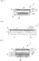
- FIG. 1 is a diagram schematically showing a cross section of a semiconductor light emitting device 1 according to an embodiment of the present invention.
- FIG. 2 is a front view of the semiconductor light emitting device 1 shown in FIG. 1 viewed from a light extraction surface.
- the semiconductor light emitting device 1 includes a semiconductor stacked layer 2 which is an LED and a light extraction surface 3a for extracting light emitted from the semiconductor stacked layer 2 to the outside.
- the light extraction surface 3a may be substantially perpendicular to the semiconductor stacked layer 2.
- the light extraction surface 3a is perpendicular at least to an active layer (p-n junction layer) which is an intermediate layer of the semiconductor stacked layer 2, the light extraction surface 3a can be regarded as being perpendicular or substantially perpendicular to the semiconductor stacked layer 2.
- a GaN-based LED which is composed of a nitride-based compound semiconductor (represented by a general formula of In x Al y Ga 1-x-y N (0 ⁇ x, 0 ⁇ y, x + y ⁇ 1)) can be used as the semiconductor stacked layer 2.
- a GaN-based LED include an ultraviolet LED, a blue LED, a green LED, and the like.
- the semiconductor stacked layer 2 which constitutes an LED may be composed of another compound semiconductor such as a ZnSe-based compound semiconductor, an InGaAs-based compound semiconductor, and an AlInGaP-based compound semiconductor.
- the wavelength band of color of light emitted from the LED may be the entire region from ultraviolet light to visible light.
- the semiconductor stacked layer 2 may be formed, for example, by a metal organic chemical vapor deposition (MOCVD) method by sequentially stacking layers on a growth substrate such as a sapphire substrate. Further, the semiconductor stacked layer 2 may also be formed by another vapor or liquid phase deposition method.
- MOCVD metal organic chemical vapor deposition
- the semiconductor light emitting device 1 includes a light transmissive light guide member 3 disposed on the semiconductor stacked layer 2, a light reflective member 4 disposed on the light guide member 3, and a light reflective package 5 which has an open portion corresponding to the light extraction surface 3a and surrounds peripheral surfaces of the semiconductor stacked layer 2.
- the package 5 may cover the upper surface of the light reflective member 4.
- the light transmissive light guide member 3 may be, for example, a glass substrate.
- the light guide member 3 may have a single layer structure and may also have a multilayer structure which includes a transparent portion 31 and a wavelength conversion portion 32 which converts the wavelength of light emitted from the semiconductor stacked layer 2 and includes, for example, a phosphor, the wavelength conversion portion 32 and the transparent portion 31 being stacked.
- the light guide member 3 may be a glass substrate having a phosphor layer formed on one surface thereof.
- the light guide member 3 may seal the semiconductor stacked layer 2.
- a sealing member is preferably composed of a resin containing a phosphor.
- the sealing member may not necessarily contain a phosphor, and may be a resin that contains a diffusing material (filler or the like) or a coloring material (a pigment or the like).
- the light guide member 3 may be disposed in contact with the semiconductor stacked layer 2, and may also be disposed on the semiconductor stacked layer 2 with a certain kind of medium layer such as a transparent adhesive layer interposed therebetween. Further, the light guide member 3 may also be disposed on the semiconductor stacked layer 2 with a growth substrate such as a sapphire substrate that is used for forming the semiconductor stacked layer 2 interposed therebetween.
- the light reflective member 4 is preferably a DBR (Distributed Bragg Reflector) which is formed on the surface of the light guide member 3.
- the DBR is a diffraction grating having a spatial period of ⁇ /2n (wherein ⁇ denotes the wavelength of light in vacuum, and n denotes the refractive index of a medium (specifically, the light guide member)).
- the light reflective member 4 which is the DBR has a function of reflecting light emitted from the semiconductor stacked layer 2 toward the light guide member 3. Accordingly, light emitted from the semiconductor stacked layer 2 is efficiently guided to the light extraction surface 3a through the light guide member 3.
- the light reflective member 4 may be formed of metal having light reflectivity or glossiness such as Ag and Al.
- the light reflective member 4 may be a stacked body of a metal layer and a DBR layer.
- the package 5 is preferably formed of a thermosetting resin such as a silicone resin and an epoxy resin.
- the package 5 may be formed of an electrically insulating material.
- the thermosetting resin preferably includes one kind of oxide selected from the group consisting of Ti oxide, Zr oxide, Nb oxide, Al oxide, and Si oxide or at least one selected from AlN and MgF.
- at least one selected from the group consisting of TiO 2 , ZrO 2 , Nb 2 O 5 , Al 2 O 3 , MgF, AlN, and SiO 2 is preferably mixed with the thermosetting resin.
- thermoplastic resin that can be transfer-molded may be used in addition to the above resins.
- the package 5 having both light reflectivity and electrically insulating property as described above may be integrated with an insulating member which electrically insulates an n-electrode 11 and a p-electrode 12 both connected to the semiconductor stacked layer 2. Accordingly, the structure of the semiconductor light emitting device 1 is simplified, and the number of manufacturing processes is reduced.
- the light extraction surface 3a of the semiconductor light emitting device 1 includes the end surface of the transparent portion 31 and the end surface of the wavelength conversion portion 32. Further, an end part of the semiconductor stacked layer 2, the end part corresponding to the light extraction surface 3a, is covered with the package 5. Therefore, light emitted from the end part of the semiconductor stacked layer 2 corresponding to the light extraction surface 3a is suppressed. As a result, color unevenness can be suppressed.
- FIG. 3 is a cross-sectional view of a semiconductor light emitting device according to a first embodiment of the present invention.
- a semiconductor light emitting device 1 includes a semiconductor stacked layer 2 which constitutes an LED as a light emitting element, and an n-electrode 11 and p-electrode 12 each formed on the lower surface of the semiconductor stacked layer 2.
- the n-electrode 11 is disposed behind the p-electrode 12 as shown in FIG. 2 .
- the semiconductor light emitting device 1 emits light in such a manner that a forward current is supplied to the semiconductor stacked layer 2 to thereby move carriers to an active layer 23 so as to be trapped therein and recombination of the carriers efficiently occurs in the active layer 23.
- the active layer 23 is also called a light emitting layer.
- an n-type semiconductor layer 21, the active layer 23, and a p-type semiconductor layer 22 are stacked in this order on a growth substrate 30.
- the active layer 23 has a quantum well structure.
- a nitride semiconductor is used as the semiconductor stacked layer 2.
- the n-type semiconductor layer 21 includes a GaN layer that contains Si
- the p-type semiconductor layer 22 includes a GaN layer that contains Mg or Zn.
- the active layer 23 includes a GaN layer or an InGaN layer. The active layer 23 emits blue light.
- the n-electrode 11 as a cathode of the LED is electrically joined to the n-type semiconductor layer 21.
- the p-electrode 12 as an anode of the LED is electrically joined to the p-type semiconductor layer 22.
- an under barrier metal (UBM) film is formed at a predetermined position in each of the n-type semiconductor layer 21 and the p-type semiconductor layer 22 by sputtering or the like and the formed UBM film is then plated with conductive metal with excellent wettability, for example, Au, thereby obtaining the n-electrode 11 and the p-electrode 12 in a bump form.
- a light reflective layer (not illustrated) may be disposed on the lower surface of the p-type semiconductor layer 22.
- the light reflective layer may be, for example, a DBR that is formed as a part of the p-type semiconductor. That is, the light reflective layer which is composed of the DBR can diffract light that has been emitted from the active layer 23 toward the electrodes 11, 12 to the opposite side and supply a forward current to the active layer 23 and the n-type semiconductor layer 21.
- a metal layer having high reflectivity such as an Ag layer and an Al layer can be used as the light reflective layer. Such a metal layer can serve as a part of the p-electrode 12.
- a light extraction surface 3a of the semiconductor light emitting device 1 is formed on one side surface of the semiconductor light emitting device 1 so as to be perpendicular to the semiconductor stacked layer 2.
- a light transmissive light guide member 3 is disposed on the semiconductor stacked layer 2 with the growth substrate (sapphire substrate) 30 interposed therebetween.
- the light guide member 3 may be disposed in contact with the semiconductor stacked layer 2 after the growth substrate 30 is removed by a laser lift off (LLO) method.
- LLO laser lift off
- the light guide member 3 includes a transparent portion 31 which is a transparent glass substrate, and a wavelength conversion portion 32 which is a phosphor layer.
- the phosphor layer is formed on one surface of the glass substrate in the light guide member 3.
- the wavelength conversion portion 32 may contain, for example, a nitride-based or oxynitride-based phosphor activated by a lanthanoid-based element such as Ce and Eu. More specifically, for example, a rare earth aluminate phosphor activated by a lanthanoid-based element such as Ce may be used as the phosphor, and a YAG-based phosphor is preferably used. In the YAG-based phosphor, a part or the entire of Y may be substituted with Tb or Lu. Further, Ce-activated rare earth silicate may be used as the material of the phosphor.
- alkaline earth halogen apatite, alkaline earth metal borate halogen, alkaline earth metal aluminate, alkaline earth metal sulfide, alkaline earth metal thiogallate, alkaline earth metal silicon nitride, or alkaline earth metal germanate activated by a lanthanoid-based element such as Eu, or an organic body or an organic complex activated by a lanthanoid-based element such as Eu may be used as the material of the phosphor.
- red phosphor examples include a SCASN-based phosphor such as (Sr, Ca)AlSiN 3 :Eu, a CASN-based phosphor such as CaAlSiN3:Eu, and SrAlSiN 3 :Eu.
- a phosphor that absorbs blue light emitted from a light emitting element and emits green light for example, a chlorosilicate phosphor or a ⁇ -sialon phosphor may be used as the material.
- the semiconductor light emitting device 1 includes a light reflective member 4 which is disposed on the light guide member 3.
- the light reflective member 4 is a DBR which is formed on the surface of the wavelength conversion portion 32 of the light guide member 3.
- the light reflective member 4 may also be metal having light reflectivity or glossiness such as Ag and Al.
- the light reflective member 4 may also be a stacked body of metal and a DBR.
- the semiconductor light emitting device 1 includes a package 5 which has an open portion corresponding to the light extraction surface 3a and surrounds peripheral surfaces of the semiconductor stacked layer 2.
- the material of the package 5 is an electrically insulating thermosetting resin such as a silicone resin and an epoxy resin.
- the material of the package 5 includes one kind of oxide selected from the group consisting of Ti oxide, Zr oxide, Nb oxide, Al oxide, and Si oxide or at least one selected from AlN and MgF so that the package 5 has a light reflective white color.
- at least one selected from the group consisting of TiO 2 , ZrO 2 , Nb 2 O 5 , Al 2 O 3 , MgF, AlN, and SiO 2 is preferably mixed with the resin.
- These resin materials can impart preferred electrically insulating property, mechanical strength, and light reflectivity to the package 5.
- the semiconductor light emitting device 1 includes the light reflective member 4 disposed on the light guide member 3, and the light reflective package 5 which has the open portion corresponding to the light extraction surface 3a and surrounds the peripheral surfaces of the semiconductor stacked layer 2. Accordingly, light emitted from the semiconductor stacked layer 2 is reflected by the light reflective member 4 and the package 5, and efficiently guided to the light extraction surface 3a through the light guide member 3. As a result, the semiconductor light emitting device 1 that achieves downsizing and high luminance is provided. Further, by increasing the light emission area in the semiconductor stacked layer 2 in the lateral direction, it is possible to increase the light emission intensity. Therefore, it is possible to increase luminous fluxes to be emitted without increasing the area of the light extraction surface 3a.
- the semiconductor light emitting device that includes the package having a dimension of 2 mm ⁇ 1 mm and a thickness of 0.3 mm is used.
- the dimension of the package is not particularly limited.
- a plurality of light emitting elements 40 are prepared.
- the semiconductor stacked layer 2 which is an LED, the n-electrode 11, the p-electrode 12, a predetermined protective film layer, and the like are formed on the growth substrate 30.
- the semiconductor stacked layer 2 is formed of a nitride-based semiconductor such as GaN.
- a sapphire single crystal substrate is used as the growth substrate 30.
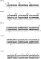
- the plurality of light emitting elements 40 are placed on an adhesive sheet 41 so that the growth substrates 30 face upward and the n-electrodes 11 and the p-electrodes 12 are in contact with the adhesive sheet 41 ( FIG. 4A ). Then, the light guide member 3 is disposed on the growth substrate 30 ( FIG. 4B ). In the light guide member 3, the light reflective member 4 is previously formed on a surface opposite to a surface on which the light emitting element 40 is disposed. In the light guide member 3 of the present embodiment, the wavelength conversion portion 32 which includes a YAG-based phosphor is stacked on the transparent portion 31 which is a transparent glass substrate. Further, a DBR as the light reflective member 4 is formed on the surface of the wavelength conversion portion 32.
- the light guide member is disposed on the growth substrate over and across at least two adjacent light emitting elements.
- a light reflective insulating member 51 is disposed to fill a gap between the plurality of light emitting elements 40 ( FIG. 4C ).
- the insulating member 51 is the material of the package 5.
- the insulating member 51 is a silicone thermosetting resin mixed with at least one selected from the group consisting of TiO 2 , ZrO 2 , Nb 2 O 5 , Al 2 O 3 , MgF, AlN, and SiO 2 .
- the insulating member 51 is also filled into a gap between the electrodes 11, 12 in order to insulate the electrodes 11, 12 of the light emitting element 40.
- a general molding method such as a compression molding method, a transfer molding method, and an injection molding method can be employed.
- pad electrodes 42 which are electrically connected to the electrodes 11, 12 of the light emitting elements 40 may be optionally formed ( FIG. 4D ).
- the insulating member 51 and the light guide member 3 are cut at a position between at least two adjacent light emitting elements 40 ( FIG. 4E ).
- a method for cutting the insulating member 51 and the light guide member 3 for example, dicing or diamond cut is used.
- the semiconductor light emitting device 1 that achieves downsizing and high luminance is provided through the manufacturing processes as described above.
- the light extraction surface 3a of the semiconductor light emitting device 1 includes the end surface of the transparent portion 31 and the end surface of the wavelength conversion portion 32. Further, in a case that an end part of the semiconductor stacked layer 2, the end part corresponding to the light extraction surface 3a, is covered with the insulating member 51, light emitted from the end part of the semiconductor stacked layer 2 corresponding to the light extraction surface 3a is suppressed. As a result, color unevenness can be suppressed.
- FIG. 5 is a cross-sectional view of a semiconductor light emitting device according to a second embodiment of the present invention.
- a semiconductor light emitting device 1 includes a semiconductor stacked layer 2 which constitutes an LED as a light emitting element, and an n-electrode 11 and p-electrode 12 each formed on the lower surface of the semiconductor stacked layer 2.
- a pad electrode may be formed in contact with the n-electrode 11 and the p-electrode 12.
- the n-electrode 11 is disposed behind the p-electrode 12 as shown in FIG. 2 .
- a light extraction surface of the semiconductor light emitting device 1 is formed on one side surface of the semiconductor light emitting device 1 so as to be perpendicular to the semiconductor stacked layer 2.
- a light guide member 3 which includes a transparent portion 31 and a wavelength conversion portion 32 is disposed on the semiconductor stacked layer 2 with a growth substrate 30 interposed therebetween.
- the transparent portion 31 is a transparent glass substrate.
- the wavelength conversion portion 32 is a YAG-based phosphor.
- the transparent portion 31 of the light guide member 3 is in contact with the growth substrate 30.
- a light reflective member 4 is disposed on the light guide member 3.
- the light reflective member 4 includes two layers, specifically, a metal layer 46 which contains a metallic element having light reflectivity or glossiness such as Ag and Al and a DBR 47.
- the metal layer 46 is disposed on the surface of the wavelength conversion portion (YAG) 32 with the DBR 47 interposed therebetween.
- the metal layer 46 may be directly disposed on the surface of the wavelength conversion portion (YAG) 32 without the DBR interposed therebetween.
- the semiconductor light emitting device 1 includes a package 5 which has an open portion corresponding to the light extraction surface and surrounds peripheral surfaces of the semiconductor stacked layer 2, the light guide member 3, and the light reflective member 4.
- the material of the package 5 is an electrically insulating thermosetting resin such as a silicone resin. At least one selected from the group consisting of TiO 2 , ZrO 2 , Nb 2 O 5 , Al 2 O 3 , MgF, AlN, and SiO 2 is mixed with the thermosetting resin of the package 5. These resin materials can impart preferred electrically insulating property, mechanical strength, and light reflectivity to the package 5.
- the semiconductor light emitting device 1 includes the light reflective package 5 which has the open portion corresponding to the light extraction surface and surrounds the peripheral surfaces of the semiconductor stacked layer 2, the light guide member 3, and the light reflective member 4. Accordingly, light emitted from the semiconductor stacked layer 2 is reflected by the light reflective member 4 and the package 5, and efficiently guided to the light extraction surface through the light guide member 3. As a result, the semiconductor light emitting device that achieves downsizing and high luminance is provided. Further, by increasing the light emission area in the semiconductor stacked layer 2 in the lateral direction, it is possible to increase the light emission intensity. Therefore, it is possible to increase luminous fluxes to be emitted without increasing the area of the light extraction surface.
- An end part of the semiconductor stacked layer 2, the end part corresponding to the light extraction surface 3a, is covered with the insulating member 5 . Therefore, light emitted from the end part of the semiconductor stacked layer 2 corresponding to the light extraction surface 3a is suppressed. As a result, color unevenness can be suppressed.
- the transparent portion 31 and the wavelength conversion portion 32 are stacked in this order on the growth substrate 30.
- the DBR 47 and the metal layer 46 are stacked in this order on the wavelength conversion portion 32.
- FIG. 6 is a cross-sectional view of a semiconductor light emitting device according to a third embodiment of the present invention.
- a semiconductor light emitting device 1 includes a semiconductor stacked layer 2 which constitutes an LED as a light emitting element, and an n-electrode 11 and p-electrode 12 each formed on the lower surface of the semiconductor stacked layer 2.
- a pad electrode may be formed in contact with the n-electrode 11 and the p-electrode 12.
- the n-electrode 11 is disposed behind the p-electrode 12 as shown in FIG. 2 .
- a light extraction surface of the semiconductor light emitting device 1 is formed on one side surface of the semiconductor light emitting device 1 so as to be perpendicular to the semiconductor stacked layer 2. Further, the semiconductor light emitting device 1 includes a package 5 which has an open portion corresponding to the light extraction surface and surrounds peripheral surfaces of the semiconductor stacked layer 2, a light guide member 3, and a light reflective member 4.
- the material of the package 5 is an electrically insulating thermosetting resin such as a silicone resin. At least one selected from the group consisting of TiO 2 , ZrO 2 , Nb 2 O 5 , Al 2 O 3 , MgF, AlN, and SiO 2 is mixed with the thermosetting resin of the package 5.
- the light guide member 3 which includes a transparent portion 31 and a wavelength conversion portion 32 is disposed on the semiconductor stacked layer 2 after a growth substrate (not illustrated) is removed by a laser lift off (LLO) method.
- the transparent portion 31 is a transparent glass substrate.
- the wavelength conversion portion 32 is a YAG-based phosphor. In the present embodiment, as illustrated in FIG. 6 , the transparent portion 31 of the light guide member 3 is in contact with the semiconductor stacked layer 2.
- the light reflective member 4 is disposed on the light guide member 3.
- the light reflective member 4 is a stacked body of a DBR 47 and a metal layer 46 which contains a metallic element having light reflectivity or glossiness such as Ag and Al.
- the metal layer 46 is disposed on the surface of the wavelength conversion portion (YAG) 32 with the DBR 47 interposed therebetween.
- the metal layer 46 may be directly disposed on the surface of the wavelength conversion portion (YAG) 32 without the DBR interposed therebetween.
- a width X between the end of the semiconductor stacked layer 2 and the end of the package 5 on the side corresponding to the light extraction surface is several ⁇ m or more, and preferably 30 ⁇ m or more.
- the width X is 50 ⁇ m.
- a width Y between the end of the semiconductor stacked layer 2 and the end of the package 5 on the side opposite to the light extraction surface is 50 ⁇ m or more, and preferably 100 ⁇ m or more.
- a thickness Z of the package 5 above the light reflective member 4 is preferably 5 ⁇ m or more. Accordingly, it is possible to achieve higher luminance in the semiconductor light emitting device.
- an insulating member continuously covers the end part of the semiconductor stacked layer 2 through the upper surface of the metal layer 46. Therefore, it is possible to suppress light leaking to the upper side of the semiconductor light emitting device 1.
- the semiconductor light emitting device 1 includes the light reflective package 5 which has the open portion corresponding to the light extraction surface and surrounds the peripheral surfaces of the semiconductor stacked layer 2, the light guide member 3, and the light reflective member 4. Accordingly, light emitted from the semiconductor stacked layer 2 is reflected by the light reflective member 4 and the package 5, and efficiently guided to the light extraction surface through the light guide member 3. As a result, the semiconductor light emitting device that achieves downsizing and high luminance is provided. Further, by increasing the light emission area in the semiconductor stacked layer 2 in the lateral direction, it is possible to increase the light emission intensity. Therefore, it is possible to increase luminous fluxes to be emitted without increasing the area of the light extraction surface. More specifically, it is possible to increase the area of the semiconductor light emitting layer in the depth direction while maintaining the size of the light extraction surface of the semiconductor light emitting device and thereby achieve high luminance.
- FIG. 7 is a cross-sectional view of a semiconductor light emitting device according to a fourth embodiment of the present invention.
- a semiconductor light emitting device 1 includes a semiconductor stacked layer 2 which constitutes an LED as a light emitting element, and an n-electrode 11 and p-electrode 12 each formed on the lower surface of the semiconductor stacked layer 2.
- a pad electrode may be formed in contact with the n-electrode 11 and the p-electrode 12.
- the n-electrode 11 is disposed behind the p-electrode 12 as shown in FIG. 2 .
- a light extraction surface of the semiconductor light emitting device 1 is formed on one side surface of the semiconductor light emitting device 1 so as to be perpendicular to the semiconductor stacked layer 2. Further, the semiconductor light emitting device 1 includes a package 5 which has an open portion corresponding to the light extraction surface and surrounds peripheral surfaces of the semiconductor stacked layer 2, a light guide member 3, and a metal layer 46.
- the material of the package 5 is an electrically insulating thermosetting resin such as a silicone resin. At least one selected from the group consisting of TiO 2 , ZrO 2 , Nb 2 O 5 , Al 2 O 3 , MgF, AlN, and SiO 2 is mixed with the thermosetting resin of the package 5. These resin materials can impart preferred electrically insulating property, mechanical strength, and light reflectivity to the package 5.
- the light guide member 3 which includes a transparent portion 31 and a wavelength conversion portion 32 is disposed on the semiconductor stacked layer 2 after a growth substrate (not illustrated) is removed by an LLO method.
- the transparent portion 31 is a transparent glass substrate.
- the wavelength conversion portion 32 is a YAG-based phosphor.
- the metal layer 46 which contains a metallic element having light reflectivity or glossiness such as Ag and Al is formed on the transparent portion (glass substrate) 31 by an electroless plating method or the like.
- a DBR (not illustrated) may be formed on the transparent portion (glass substrate) 31, and the metal layer 46 may be formed on the DBR.
- the wavelength conversion portion (YAG) 32 is adhered to the semiconductor stacked layer 2 with an adhesive layer 61 interposed therebetween.
- the adhesive layer 61 is formed of a transparent resin material.
- the semiconductor light emitting device 1 includes the light reflective package 5 which has the open portion corresponding to the light extraction surface and surrounds the peripheral surfaces of the semiconductor stacked layer 2, the light guide member 3, and the metal layer 46. Accordingly, light emitted from the semiconductor stacked layer 2 is reflected by the metal layer 46 and the package 5, and efficiently guided to the light extraction surface through the light guide member 3. As a result, the semiconductor light emitting device that achieves downsizing and high luminance is provided. Further, by increasing the light emission area in the semiconductor stacked layer 2 in the lateral direction, it is possible to increase the light emission intensity. Therefore, it is possible to increase luminous fluxes to be emitted without increasing the area of the light extraction surface.
- FIG. 8 is a cross-sectional view of a semiconductor light emitting device according to a fifth embodiment of the present invention.
- a semiconductor light emitting device 1 includes a semiconductor stacked layer 2 which constitutes an LED as a light emitting element, and an n-electrode 11 and p-electrode 12 each formed on the lower surface of the semiconductor stacked layer 2.
- a pad electrode may be formed in contact with the n-electrode 11 and the p-electrode 12.
- the n-electrode 11 is disposed behind the p-electrode 12 as shown in FIG. 2 .
- a light extraction surface of the semiconductor light emitting device 1 is formed on one side surface of the semiconductor light emitting device 1 so as to be perpendicular to the semiconductor stacked layer 2. Further, the semiconductor light emitting device 1 includes a package 5 which has an open portion corresponding to the light extraction surface and surrounds peripheral surfaces of the semiconductor stacked layer 2, a wavelength conversion portion 32, and a light reflective member 4.
- the material of the package 5 is an electrically insulating thermosetting resin such as a silicone resin. At least one selected from the group consisting of TiO 2 , ZrO 2 , Nb 2 O 5 , Al 2 O 3 , MgF, AlN, and SiO 2 is mixed with the thermosetting resin of the package 5.
- the wavelength conversion portion 32 which is a YAG-based phosphor is disposed on the semiconductor stacked layer 2 with a growth substrate 30 interposed therebetween.
- the wavelength conversion portion 32 is directly joined to the growth substrate 30 of the semiconductor stacked layer 2.
- Direct joining indicates that surfaces to be joined are joined by atomic bond without using an adhesive.
- Direct joining that can be used here is preferably a joining method that is generally classified as room-temperature joining.
- Direct joining also includes a method that accelerates a chemical reaction or diffusion for joining at an extremely high temperature.
- such a method is not preferred in LED production of the present invention because of temperature limitation.
- such a method is also not preferred because there is concern about a surface layer material that is required for applying an electric field and the influence on the semiconductor.
- Examples of a direct joining method suitable for the present embodiment include surface activation joining, atomic diffusion joining, and hydroxyl group joining.
- surface activation joining inert ions are applied to the joining interface in ultrahigh vacuum to thereby clean and activate the surface to perform joining.
- atomic diffusion joining metal is sputtered also in ultrahigh vacuum and joining is performed using diffusion of the metal. It has been confirmed that, by making the sputtered film extremely thin, the joining can be performed without affecting extraction of light.
- hydroxyl group joining a hydroxyl group is formed on the joining interface and joining is performed using hydrogen bond of the hydroxyl group.
- the above three joining methods are all room-temperature joining methods. However, a bonding power may increase by performing heat treatment as needed. In this case, heating can be performed at 400°C or less, preferably at 300°C or less, and more preferably at 200°C or less.
- direct joining indicates that different kinds of materials are joined without an organic material such as an adhesive interposed therebetween. Even when metal or a dielectric substance is introduced as an intermediate member, the optical characteristic of the intermediate member is ignored when introducing light into a joining member.
- a YAG phosphor can be used as the joining member.
- the light reflective member 4 is disposed on the wavelength conversion portion 32.
- the light reflective member 4 includes two layers, specifically, a DBR 47 and a metal layer 46 which contains a metallic element having light reflectivity or glossiness such as Ag and Al.
- the metal layer 46 is disposed on the surface of the wavelength conversion portion (YAG) 32 with the DBR 47 interposed therebetween.
- the metal layer 46 may be directly disposed on the surface of the wavelength conversion portion (YAG) 32 without the DBR 47 interposed therebetween.
- the semiconductor light emitting device 1 includes the light reflective package 5 which has the open portion corresponding to the light extraction surface and surrounds the peripheral surfaces of the semiconductor stacked layer 2, the wavelength conversion portion (YAG) 32, and the light reflective member 4. Accordingly, light emitted from the semiconductor stacked layer 2 is reflected by the light reflective member 4 and the package 5, then wavelength-converted by the wavelength conversion portion (YAG) 32, and then efficiently guided to the light extraction surface. As a result, the semiconductor light emitting device that achieves downsizing and high luminance is provided. Further, by increasing the light emission area in the semiconductor stacked layer 2 in the lateral direction, it is possible to increase the light emission intensity. Therefore, it is possible to increase luminous fluxes to be emitted without increasing the area of the light extraction surface.
- FIG. 9 is a cross-sectional view of a semiconductor light emitting device according to a sixth embodiment of the present invention.
- a semiconductor light emitting device 1 includes a semiconductor stacked layer 2 which constitutes an LED as a light emitting element, and an n-electrode 11 and p-electrode 12 each formed on the lower surface of the semiconductor stacked layer 2.
- a pad electrode may be formed in contact with the n-electrode 11 and the p-electrode 12.
- the n-electrode 11 is disposed behind the p-electrode 12 as shown in FIG. 2 .
- a light extraction surface of the semiconductor light emitting device 1 is formed on one side surface of the semiconductor light emitting device 1 so as to be perpendicular to the semiconductor stacked layer 2.
- a BPF (Band Pass Filter) 33 which has an open portion corresponding to the light extraction surface, a wavelength conversion portion 32, and a light reflective member 4 are stacked in this order on the semiconductor stacked layer 2.
- the semiconductor light emitting device 1 includes a package 5 which surrounds outer peripheral surfaces of the light reflective member 4. The above-described resins can be used as the material of the package 5.
- the wavelength conversion portion 32 which is a YAG-based phosphor is disposed on a growth substrate 30 of the semiconductor stacked layer 2 with the BPF 33 interposed therebetween.
- the BPF 33 is an optical filter that transmits light having a wavelength band of, for example, 420 to 500 nm.
- the wavelength band of the BPF 33 is preferably 430 to 470 nm.
- a peak of the LED that is composed of the nitride-based semiconductor stacked layer 2 is 450 nm.
- the light reflective member 4 is disposed on the wavelength conversion portion 32.
- the light reflective member 4 includes two layers, specifically, a DBR 47 and a metal layer 46 which contains a metallic element having light reflectivity or glossiness such as Ag and Al.
- the metal layer 46 is disposed on the surface of the wavelength conversion portion (YAG) 32 with the DBR 47 interposed therebetween.
- the metal layer 46 may be directly disposed on the surface of the wavelength conversion portion (YAG) 32 without the DBR 47 interposed therebetween.
- FIG. 10 is a cross-sectional view of a semiconductor light emitting device according to a seventh embodiment of the present invention.
- a semiconductor light emitting device 1 includes a semiconductor stacked layer 2 which constitutes an LED as a light emitting element, and an n-electrode 11 and p-electrode 12 each formed on the lower surface of the semiconductor stacked layer 2.
- a pad electrode may be formed in contact with the n-electrode 11 and the p-electrode 12.
- the n-electrode 11 is disposed behind the p-electrode 12 as shown in FIG. 2 .
- a light extraction surface of the semiconductor light emitting device 1 is formed on one side surface of the semiconductor light emitting device 1 so as to be perpendicular to the semiconductor stacked layer 2. Further, the semiconductor light emitting device 1 includes a package 5 which has an open portion corresponding to the light extraction surface and surrounds peripheral surfaces of the semiconductor stacked layer 2, a BPF 33, a wavelength conversion portion 32, and a light reflective member 4. The above-described resins can be used as the material of the package 5.
- a light guide member which includes the BPF 33 and the wavelength conversion portion 32 which is a YAG-based phosphor is disposed on the semiconductor stacked layer 2 after a growth substrate (not illustrated) is removed by an LLO method.
- the BPF 33 is in contact with the semiconductor stacked layer 2.
- the BPF 33 is an optical filter that transmits light having a wavelength band of, for example, 420 to 500 nm.
- the wavelength band of the BPF 33 is preferably 430 to 470 nm.
- a peak of the LED that is composed of the nitride-based semiconductor stacked layer 2 is 450 nm.
- the light reflective member 4 includes two layers, specifically, a DBR 47 and a metal layer 46 which contains a metallic element having light reflectivity or glossiness such as Ag and Al.
- the metal layer 46 is disposed on the surface of the wavelength conversion portion (YAG) 32 with the DBR 47 interposed therebetween.
- the metal layer 46 may be directly disposed on the surface of the wavelength conversion portion (YAG) 32 without the DBR 47 interposed therebetween.
- FIG. 11 is a cross-sectional view of a semiconductor light emitting device according to an eighth embodiment of the present invention.
- FIG. 12 is a perspective view of the semiconductor light emitting device of FIG. 11 .
- the semiconductor light emitting device in each of the third to seventh embodiments described above also has the same appearance as illustrated in FIG. 12 .
- a semiconductor light emitting device 1 includes a semiconductor stacked layer 2 which constitutes an LED as a light emitting element and an n-electrode 11 and p-electrode 12 each formed on the lower surface of the semiconductor stacked layer 2.
- the n-electrode 11 is disposed behind the p-electrode 12 as shown in FIG. 2 .
- a light extraction surface of the semiconductor light emitting device 1 is formed on one side surface of the semiconductor light emitting device 1 so as to be perpendicular to the semiconductor stacked layer 2.
- a package 5 of the semiconductor light emitting device 1 has an open portion corresponding to the light extraction surface and houses the semiconductor stacked layer 2 therein. The semiconductor stacked layer 2 housed in the package 5 is sealed by a sealing member 34.
- the sealing member 34 is composed of a light transmissive resin that contains a YAG-based phosphor.
- the sealing member 34 may not necessarily contain a phosphor, and may be a resin that contains a diffusing material (a filler or the like) or a coloring material (a pigment or the like).
- the above-described resins can be used as the material of the package 5.
- the semiconductor light emitting device 1 includes the light reflective package 5 which has the open portion corresponding to the light extraction surface and houses the semiconductor stacked layer 2 therein. Accordingly, light emitted from the semiconductor stacked layer 2 is reflected inside the package 5, and efficiently guided to the light extraction surface through the sealing member 34. As a result, the semiconductor light emitting device that achieves downsizing and high luminance is provided. Further, by increasing the light emission area in the semiconductor stacked layer 2 in the lateral direction, it is possible to increase the light emission intensity. Therefore, it is possible to increase luminous fluxes to be emitted without increasing the area of the light extraction surface.
Applications Claiming Priority (1)
| Application Number | Priority Date | Filing Date | Title |
|---|---|---|---|
| JP2013236935A JP6438648B2 (ja) | 2013-11-15 | 2013-11-15 | 半導体発光装置およびその製造方法 |
Publications (2)
| Publication Number | Publication Date |
|---|---|
| EP2874190A1 EP2874190A1 (en) | 2015-05-20 |
| EP2874190B1 true EP2874190B1 (en) | 2019-09-18 |
Family
ID=51893946
Family Applications (1)
| Application Number | Title | Priority Date | Filing Date |
|---|---|---|---|
| EP14193319.2A Active EP2874190B1 (en) | 2013-11-15 | 2014-11-14 | Semiconductor light emitting device having light extraction surface perpendicular to the surface of the stacked semiconductor layer and method for manufacturing the same |
Country Status (4)
| Country | Link |
|---|---|
| US (2) | US10211379B2 (ja) |
| EP (1) | EP2874190B1 (ja) |
| JP (1) | JP6438648B2 (ja) |
| CN (1) | CN104659172B (ja) |
Families Citing this family (20)
| Publication number | Priority date | Publication date | Assignee | Title |
|---|---|---|---|---|
| KR20160038094A (ko) * | 2014-09-26 | 2016-04-07 | 코닝정밀소재 주식회사 | 발광 다이오드의 색변환용 기판 및 그 제조방법 |
| CN106549094B (zh) * | 2015-09-18 | 2020-03-10 | 新世纪光电股份有限公司 | 发光元件封装结构 |
| KR102417181B1 (ko) | 2015-11-09 | 2022-07-05 | 삼성전자주식회사 | 발광 패키지, 반도체 발광 소자, 발광 모듈 및 발광 패키지의 제조 방법 |
| JP6645213B2 (ja) * | 2016-01-27 | 2020-02-14 | オムロン株式会社 | 発光装置、および発光装置の製造方法 |
| JP6414104B2 (ja) | 2016-02-29 | 2018-10-31 | 日亜化学工業株式会社 | 発光装置の製造方法 |
| JP6315014B2 (ja) * | 2016-03-23 | 2018-04-25 | 日亜化学工業株式会社 | 半導体装置の製造方法 |
| DE102016109308B4 (de) * | 2016-05-20 | 2024-01-18 | OSRAM Opto Semiconductors Gesellschaft mit beschränkter Haftung | Strahlungsemittierendes bauelement |
| JP6575436B2 (ja) * | 2016-05-31 | 2019-09-18 | 日亜化学工業株式会社 | 発光装置の製造方法 |
| JP6245587B1 (ja) | 2016-10-28 | 2017-12-13 | 大学共同利用機関法人自然科学研究機構 | レーザー部品 |
| JP6809203B2 (ja) | 2016-12-20 | 2021-01-06 | 日亜化学工業株式会社 | 発光装置の製造方法 |
| TWI644056B (zh) * | 2017-07-21 | 2018-12-11 | 行家光電股份有限公司 | 具非對稱結構的發光裝置、包含該發光裝置之背光模組及該發光裝置之製造方法 |
| US10749086B2 (en) | 2017-07-21 | 2020-08-18 | Maven Optronics Co., Ltd. | Asymmetrically shaped light-emitting device, backlight module using the same, and method for manufacturing the same |
| CN109411590B (zh) * | 2017-08-17 | 2020-01-07 | 光宝光电(常州)有限公司 | 发光二极管结构及发光单元 |
| EP3457444A1 (en) * | 2017-09-19 | 2019-03-20 | ams AG | Phosphor-converted light-emitting device |
| JP6909695B2 (ja) * | 2017-10-02 | 2021-07-28 | 株式会社小糸製作所 | 波長変換部材および光源モジュール |
| WO2019074873A1 (en) * | 2017-10-10 | 2019-04-18 | Lumileds Llc | LED HOUSING COMPRISING A CONVERTER CONFINEMENT |
| JP6743801B2 (ja) | 2017-10-27 | 2020-08-19 | 日亜化学工業株式会社 | 発光装置の製造方法 |
| DE102018106972B4 (de) * | 2018-03-23 | 2024-05-02 | OSRAM Opto Semiconductors Gesellschaft mit beschränkter Haftung | Optoelektronisches bauelement mit reflektiver vergussmasse und verfahren zur herstellung eines optoelektronischen bauelements |
| JP6876274B2 (ja) | 2018-11-14 | 2021-05-26 | 日亜化学工業株式会社 | 発光素子、発光装置及び発光素子の製造方法 |
| DE102018132651A1 (de) * | 2018-12-18 | 2020-06-18 | Osram Opto Semiconductors Gmbh | Optoelektronisches halbleiterbauteil |
Family Cites Families (34)
| Publication number | Priority date | Publication date | Assignee | Title |
|---|---|---|---|---|
| US5434426A (en) * | 1992-09-10 | 1995-07-18 | Kabushiki Kaisha Toshiba | Optical interconnection device |
| JP4177049B2 (ja) * | 2002-08-28 | 2008-11-05 | シャープ株式会社 | 表面実装型側面発光ダイオードおよびその製造方法 |
| JP2005166937A (ja) * | 2003-12-02 | 2005-06-23 | Toyoda Gosei Co Ltd | 発光装置 |
| US20070267646A1 (en) * | 2004-06-03 | 2007-11-22 | Philips Lumileds Lighting Company, Llc | Light Emitting Device Including a Photonic Crystal and a Luminescent Ceramic |
| US7553683B2 (en) * | 2004-06-09 | 2009-06-30 | Philips Lumiled Lighting Co., Llc | Method of forming pre-fabricated wavelength converting elements for semiconductor light emitting devices |
| US8080828B2 (en) * | 2006-06-09 | 2011-12-20 | Philips Lumileds Lighting Company, Llc | Low profile side emitting LED with window layer and phosphor layer |
| DE102007010755A1 (de) * | 2007-03-06 | 2008-10-30 | Osram Opto Semiconductors Gmbh | Anordnung mit einem Halbleiterchip und einer Lichtleiterschicht |
| DE102007019776A1 (de) * | 2007-04-26 | 2008-10-30 | Osram Opto Semiconductors Gmbh | Optoelektronisches Bauelement und Verfahren zur Herstellung einer Mehrzahl optoelektronischer Bauelemente |
| US9046634B2 (en) * | 2007-06-14 | 2015-06-02 | Philips Lumileds Lighting Company, Llc | Thin flash or video recording light using low profile side emitting LED |
| US7652301B2 (en) | 2007-08-16 | 2010-01-26 | Philips Lumileds Lighting Company, Llc | Optical element coupled to low profile side emitting LED |
| CN101878540B (zh) | 2007-11-29 | 2013-11-06 | 日亚化学工业株式会社 | 发光装置及其制造方法 |
| KR20100127286A (ko) | 2008-03-21 | 2010-12-03 | 코닌클리즈케 필립스 일렉트로닉스 엔.브이. | 발광 장치 |
| JP2009295611A (ja) | 2008-06-02 | 2009-12-17 | Sharp Corp | 半導体発光素子及びその製造方法 |
| US8957428B2 (en) * | 2008-09-25 | 2015-02-17 | Koninklijke Philips N.V. | Coated light emitting device and method for coating thereof |
| JP5431706B2 (ja) | 2008-10-01 | 2014-03-05 | ミネベア株式会社 | 発光装置 |
| CN102187485B (zh) * | 2008-10-15 | 2013-07-03 | 株式会社小糸制作所 | 发光模块、发光模块的制造方法及灯具单元 |
| TWI463708B (zh) * | 2009-02-24 | 2014-12-01 | Advanced Optoelectronic Tech | 側面出光型發光元件封裝結構及其製造方法 |
| JP5396215B2 (ja) * | 2009-09-24 | 2014-01-22 | スタンレー電気株式会社 | 半導体発光装置の製造方法、半導体発光装置および液晶表示装置 |
| JP5515992B2 (ja) * | 2010-04-07 | 2014-06-11 | 日亜化学工業株式会社 | 発光装置 |
| US8916399B2 (en) * | 2010-04-08 | 2014-12-23 | Nichia Corporation | Method of manufacturing light emitting device including light emitting element and wavelength converting member |
| WO2011145794A1 (ko) * | 2010-05-18 | 2011-11-24 | 서울반도체 주식회사 | 파장변환층을 갖는 발광 다이오드 칩과 그 제조 방법, 및 그것을 포함하는 패키지 및 그 제조 방법 |
| CN201754416U (zh) | 2010-07-09 | 2011-03-02 | 戴美惠 | 具有提升反射效率的led发光载体结构 |
| JP5508244B2 (ja) * | 2010-11-15 | 2014-05-28 | シチズンホールディングス株式会社 | 半導体発光装置の製造方法 |
| JP2012142326A (ja) * | 2010-12-28 | 2012-07-26 | Mitsubishi Heavy Ind Ltd | 発光素子及び発光素子の製造方法 |
| JP5745319B2 (ja) * | 2011-04-14 | 2015-07-08 | 日東電工株式会社 | 蛍光反射シート、および、発光ダイオード装置の製造方法 |
| JP2013143430A (ja) * | 2012-01-10 | 2013-07-22 | Citizen Holdings Co Ltd | 半導体発光装置及びそれを用いた照明装置 |
| JP5956167B2 (ja) * | 2012-01-23 | 2016-07-27 | スタンレー電気株式会社 | 発光装置、車両用灯具及び発光装置の製造方法 |
| JP6008940B2 (ja) * | 2012-03-13 | 2016-10-19 | シチズンホールディングス株式会社 | 半導体発光装置及びその製造方法 |
| KR101974354B1 (ko) * | 2013-02-14 | 2019-05-02 | 삼성전자주식회사 | 발광소자 패키지 및 그 제조 방법 |
| DE102013104840A1 (de) | 2013-05-10 | 2014-11-13 | Osram Opto Semiconductors Gmbh | Strahlungsemittierendes Halbleiterbauelement und Verfahren zur Herstellung von strahlungsemittierenden Halbleiterbauelementen |
| US9960330B2 (en) * | 2013-07-22 | 2018-05-01 | Koninklijke Philips N.V. | Flip-chip side emitting LED with top reflector, peripheral wavelength conversion element, and optical element between light emitting element and lightguide element |
| EP2854186A1 (en) * | 2013-09-26 | 2015-04-01 | Seoul Semiconductor Co., Ltd. | Light source module, fabrication method therefor, and backlight unit including the same |
| KR20150037680A (ko) * | 2013-09-30 | 2015-04-08 | 서울반도체 주식회사 | 광원 모듈 및 이를 구비한 백라이트 유닛 |
| TWI707484B (zh) * | 2013-11-14 | 2020-10-11 | 晶元光電股份有限公司 | 發光裝置 |
-
2013
- 2013-11-15 JP JP2013236935A patent/JP6438648B2/ja active Active
-
2014
- 2014-11-14 EP EP14193319.2A patent/EP2874190B1/en active Active
- 2014-11-14 US US14/542,271 patent/US10211379B2/en active Active
- 2014-11-17 CN CN201410653499.6A patent/CN104659172B/zh active Active
-
2018
- 2018-08-29 US US16/116,841 patent/US10777715B2/en active Active
Non-Patent Citations (1)
| Title |
|---|
| None * |
Also Published As
| Publication number | Publication date |
|---|---|
| US10777715B2 (en) | 2020-09-15 |
| CN104659172B (zh) | 2019-04-02 |
| JP6438648B2 (ja) | 2018-12-19 |
| US20150137164A1 (en) | 2015-05-21 |
| US20190019927A1 (en) | 2019-01-17 |
| JP2015097235A (ja) | 2015-05-21 |
| EP2874190A1 (en) | 2015-05-20 |
| US10211379B2 (en) | 2019-02-19 |
| CN104659172A (zh) | 2015-05-27 |
Similar Documents
| Publication | Publication Date | Title |
|---|---|---|
| US10777715B2 (en) | Semiconductor light emitting device | |
| US9620689B2 (en) | Semiconductor light emitting device and method of manufacturing the same | |
| US10230029B2 (en) | Light emitting device and method of manufacturing the same | |
| US9793448B2 (en) | Light emitting diode chip having wavelength converting layer and method of fabricating the same, and package having the light emitting diode chip and method of fabricating the same | |
| KR100693969B1 (ko) | 고체 소자 디바이스 및 그 제조 방법 | |
| JP6205897B2 (ja) | 発光装置及びその製造方法 | |
| JP6248431B2 (ja) | 半導体発光装置の製造方法 | |
| JP2011243977A (ja) | 波長変換層を有する発光ダイオードチップとその製造方法、及びそれを含むパッケージ及びその製造方法 | |
| KR20100080423A (ko) | 발광소자 패키지 및 그 제조방법 | |
| KR20080025687A (ko) | 백색 반도체 발광 소자 및 그 제법 | |
| JP6743866B2 (ja) | 半導体発光装置 | |
| CN109757120A (zh) | 发光器件封装 | |
| US11342486B2 (en) | Light-emitting device package and lighting device having same | |
| EP2390937B1 (en) | Light emitting device package comprising an optical filter between a light emitting device and a fluorescent layer | |
| JP6460189B2 (ja) | 発光装置及びその製造方法 | |
| JP6432654B2 (ja) | 半導体発光装置 | |
| KR102413220B1 (ko) | 발광소자 패키지 | |
| JP7227528B2 (ja) | 半導体発光装置 | |
| JP6978708B2 (ja) | 半導体発光装置 | |
| JP2006352038A (ja) | 白色半導体発光素子およびその製法 |
Legal Events
| Date | Code | Title | Description |
|---|---|---|---|
| PUAI | Public reference made under article 153(3) epc to a published international application that has entered the european phase |
Free format text: ORIGINAL CODE: 0009012 |
|
| 17P | Request for examination filed |
Effective date: 20141114 |
|
| AK | Designated contracting states |
Kind code of ref document: A1 Designated state(s): AL AT BE BG CH CY CZ DE DK EE ES FI FR GB GR HR HU IE IS IT LI LT LU LV MC MK MT NL NO PL PT RO RS SE SI SK SM TR |
|
| AX | Request for extension of the european patent |
Extension state: BA ME |
|
| R17P | Request for examination filed (corrected) |
Effective date: 20151118 |
|
| RBV | Designated contracting states (corrected) |
Designated state(s): AL AT BE BG CH CY CZ DE DK EE ES FI FR GB GR HR HU IE IS IT LI LT LU LV MC MK MT NL NO PL PT RO RS SE SI SK SM TR |
|
| STAA | Information on the status of an ep patent application or granted ep patent |
Free format text: STATUS: EXAMINATION IS IN PROGRESS |
|
| 17Q | First examination report despatched |
Effective date: 20181031 |
|
| GRAP | Despatch of communication of intention to grant a patent |
Free format text: ORIGINAL CODE: EPIDOSNIGR1 |
|
| STAA | Information on the status of an ep patent application or granted ep patent |
Free format text: STATUS: GRANT OF PATENT IS INTENDED |
|
| RIC1 | Information provided on ipc code assigned before grant |
Ipc: H01L 33/58 20100101ALN20190516BHEP Ipc: H01L 33/46 20100101AFI20190516BHEP Ipc: H01L 33/50 20100101ALN20190516BHEP |
|
| INTG | Intention to grant announced |
Effective date: 20190531 |
|
| GRAS | Grant fee paid |
Free format text: ORIGINAL CODE: EPIDOSNIGR3 |
|
| GRAA | (expected) grant |
Free format text: ORIGINAL CODE: 0009210 |
|
| STAA | Information on the status of an ep patent application or granted ep patent |
Free format text: STATUS: THE PATENT HAS BEEN GRANTED |
|
| AK | Designated contracting states |
Kind code of ref document: B1 Designated state(s): AL AT BE BG CH CY CZ DE DK EE ES FI FR GB GR HR HU IE IS IT LI LT LU LV MC MK MT NL NO PL PT RO RS SE SI SK SM TR |
|
| REG | Reference to a national code |
Ref country code: GB Ref legal event code: FG4D |
|
| REG | Reference to a national code |
Ref country code: CH Ref legal event code: EP |
|
| REG | Reference to a national code |
Ref country code: DE Ref legal event code: R096 Ref document number: 602014053762 Country of ref document: DE |
|
| REG | Reference to a national code |
Ref country code: AT Ref legal event code: REF Ref document number: 1182346 Country of ref document: AT Kind code of ref document: T Effective date: 20191015 |
|
| REG | Reference to a national code |
Ref country code: IE Ref legal event code: FG4D |
|
| REG | Reference to a national code |
Ref country code: NL Ref legal event code: MP Effective date: 20190918 |
|
| PG25 | Lapsed in a contracting state [announced via postgrant information from national office to epo] |
Ref country code: NO Free format text: LAPSE BECAUSE OF FAILURE TO SUBMIT A TRANSLATION OF THE DESCRIPTION OR TO PAY THE FEE WITHIN THE PRESCRIBED TIME-LIMIT Effective date: 20191218 Ref country code: BG Free format text: LAPSE BECAUSE OF FAILURE TO SUBMIT A TRANSLATION OF THE DESCRIPTION OR TO PAY THE FEE WITHIN THE PRESCRIBED TIME-LIMIT Effective date: 20191218 Ref country code: SE Free format text: LAPSE BECAUSE OF FAILURE TO SUBMIT A TRANSLATION OF THE DESCRIPTION OR TO PAY THE FEE WITHIN THE PRESCRIBED TIME-LIMIT Effective date: 20190918 Ref country code: FI Free format text: LAPSE BECAUSE OF FAILURE TO SUBMIT A TRANSLATION OF THE DESCRIPTION OR TO PAY THE FEE WITHIN THE PRESCRIBED TIME-LIMIT Effective date: 20190918 Ref country code: LT Free format text: LAPSE BECAUSE OF FAILURE TO SUBMIT A TRANSLATION OF THE DESCRIPTION OR TO PAY THE FEE WITHIN THE PRESCRIBED TIME-LIMIT Effective date: 20190918 Ref country code: HR Free format text: LAPSE BECAUSE OF FAILURE TO SUBMIT A TRANSLATION OF THE DESCRIPTION OR TO PAY THE FEE WITHIN THE PRESCRIBED TIME-LIMIT Effective date: 20190918 |
|
| REG | Reference to a national code |
Ref country code: LT Ref legal event code: MG4D |
|
| PG25 | Lapsed in a contracting state [announced via postgrant information from national office to epo] |
Ref country code: GR Free format text: LAPSE BECAUSE OF FAILURE TO SUBMIT A TRANSLATION OF THE DESCRIPTION OR TO PAY THE FEE WITHIN THE PRESCRIBED TIME-LIMIT Effective date: 20191219 Ref country code: RS Free format text: LAPSE BECAUSE OF FAILURE TO SUBMIT A TRANSLATION OF THE DESCRIPTION OR TO PAY THE FEE WITHIN THE PRESCRIBED TIME-LIMIT Effective date: 20190918 Ref country code: LV Free format text: LAPSE BECAUSE OF FAILURE TO SUBMIT A TRANSLATION OF THE DESCRIPTION OR TO PAY THE FEE WITHIN THE PRESCRIBED TIME-LIMIT Effective date: 20190918 Ref country code: AL Free format text: LAPSE BECAUSE OF FAILURE TO SUBMIT A TRANSLATION OF THE DESCRIPTION OR TO PAY THE FEE WITHIN THE PRESCRIBED TIME-LIMIT Effective date: 20190918 |
|
| REG | Reference to a national code |
Ref country code: AT Ref legal event code: MK05 Ref document number: 1182346 Country of ref document: AT Kind code of ref document: T Effective date: 20190918 |
|
| PG25 | Lapsed in a contracting state [announced via postgrant information from national office to epo] |
Ref country code: ES Free format text: LAPSE BECAUSE OF FAILURE TO SUBMIT A TRANSLATION OF THE DESCRIPTION OR TO PAY THE FEE WITHIN THE PRESCRIBED TIME-LIMIT Effective date: 20190918 Ref country code: PL Free format text: LAPSE BECAUSE OF FAILURE TO SUBMIT A TRANSLATION OF THE DESCRIPTION OR TO PAY THE FEE WITHIN THE PRESCRIBED TIME-LIMIT Effective date: 20190918 Ref country code: PT Free format text: LAPSE BECAUSE OF FAILURE TO SUBMIT A TRANSLATION OF THE DESCRIPTION OR TO PAY THE FEE WITHIN THE PRESCRIBED TIME-LIMIT Effective date: 20200120 Ref country code: IT Free format text: LAPSE BECAUSE OF FAILURE TO SUBMIT A TRANSLATION OF THE DESCRIPTION OR TO PAY THE FEE WITHIN THE PRESCRIBED TIME-LIMIT Effective date: 20190918 Ref country code: RO Free format text: LAPSE BECAUSE OF FAILURE TO SUBMIT A TRANSLATION OF THE DESCRIPTION OR TO PAY THE FEE WITHIN THE PRESCRIBED TIME-LIMIT Effective date: 20190918 Ref country code: NL Free format text: LAPSE BECAUSE OF FAILURE TO SUBMIT A TRANSLATION OF THE DESCRIPTION OR TO PAY THE FEE WITHIN THE PRESCRIBED TIME-LIMIT Effective date: 20190918 Ref country code: EE Free format text: LAPSE BECAUSE OF FAILURE TO SUBMIT A TRANSLATION OF THE DESCRIPTION OR TO PAY THE FEE WITHIN THE PRESCRIBED TIME-LIMIT Effective date: 20190918 Ref country code: AT Free format text: LAPSE BECAUSE OF FAILURE TO SUBMIT A TRANSLATION OF THE DESCRIPTION OR TO PAY THE FEE WITHIN THE PRESCRIBED TIME-LIMIT Effective date: 20190918 |
|
| PG25 | Lapsed in a contracting state [announced via postgrant information from national office to epo] |
Ref country code: IS Free format text: LAPSE BECAUSE OF FAILURE TO SUBMIT A TRANSLATION OF THE DESCRIPTION OR TO PAY THE FEE WITHIN THE PRESCRIBED TIME-LIMIT Effective date: 20200224 Ref country code: CZ Free format text: LAPSE BECAUSE OF FAILURE TO SUBMIT A TRANSLATION OF THE DESCRIPTION OR TO PAY THE FEE WITHIN THE PRESCRIBED TIME-LIMIT Effective date: 20190918 Ref country code: SM Free format text: LAPSE BECAUSE OF FAILURE TO SUBMIT A TRANSLATION OF THE DESCRIPTION OR TO PAY THE FEE WITHIN THE PRESCRIBED TIME-LIMIT Effective date: 20190918 Ref country code: SK Free format text: LAPSE BECAUSE OF FAILURE TO SUBMIT A TRANSLATION OF THE DESCRIPTION OR TO PAY THE FEE WITHIN THE PRESCRIBED TIME-LIMIT Effective date: 20190918 |
|
| REG | Reference to a national code |
Ref country code: DE Ref legal event code: R097 Ref document number: 602014053762 Country of ref document: DE |
|
| REG | Reference to a national code |
Ref country code: CH Ref legal event code: PL |
|
| PLBE | No opposition filed within time limit |
Free format text: ORIGINAL CODE: 0009261 |
|
| STAA | Information on the status of an ep patent application or granted ep patent |
Free format text: STATUS: NO OPPOSITION FILED WITHIN TIME LIMIT |
|
| PG2D | Information on lapse in contracting state deleted |
Ref country code: IS |
|
| PG25 | Lapsed in a contracting state [announced via postgrant information from national office to epo] |
Ref country code: DK Free format text: LAPSE BECAUSE OF FAILURE TO SUBMIT A TRANSLATION OF THE DESCRIPTION OR TO PAY THE FEE WITHIN THE PRESCRIBED TIME-LIMIT Effective date: 20190918 Ref country code: MC Free format text: LAPSE BECAUSE OF FAILURE TO SUBMIT A TRANSLATION OF THE DESCRIPTION OR TO PAY THE FEE WITHIN THE PRESCRIBED TIME-LIMIT Effective date: 20190918 Ref country code: LU Free format text: LAPSE BECAUSE OF NON-PAYMENT OF DUE FEES Effective date: 20191114 Ref country code: CH Free format text: LAPSE BECAUSE OF NON-PAYMENT OF DUE FEES Effective date: 20191130 Ref country code: LI Free format text: LAPSE BECAUSE OF NON-PAYMENT OF DUE FEES Effective date: 20191130 Ref country code: IS Free format text: LAPSE BECAUSE OF FAILURE TO SUBMIT A TRANSLATION OF THE DESCRIPTION OR TO PAY THE FEE WITHIN THE PRESCRIBED TIME-LIMIT Effective date: 20200119 |
|
| REG | Reference to a national code |
Ref country code: BE Ref legal event code: MM Effective date: 20191130 |
|
| 26N | No opposition filed |
Effective date: 20200619 |
|
| PG25 | Lapsed in a contracting state [announced via postgrant information from national office to epo] |
Ref country code: SI Free format text: LAPSE BECAUSE OF FAILURE TO SUBMIT A TRANSLATION OF THE DESCRIPTION OR TO PAY THE FEE WITHIN THE PRESCRIBED TIME-LIMIT Effective date: 20190918 |
|
| PG25 | Lapsed in a contracting state [announced via postgrant information from national office to epo] |
Ref country code: IE Free format text: LAPSE BECAUSE OF NON-PAYMENT OF DUE FEES Effective date: 20191114 |
|
| PG25 | Lapsed in a contracting state [announced via postgrant information from national office to epo] |
Ref country code: BE Free format text: LAPSE BECAUSE OF NON-PAYMENT OF DUE FEES Effective date: 20191130 |
|
| PG25 | Lapsed in a contracting state [announced via postgrant information from national office to epo] |
Ref country code: CY Free format text: LAPSE BECAUSE OF FAILURE TO SUBMIT A TRANSLATION OF THE DESCRIPTION OR TO PAY THE FEE WITHIN THE PRESCRIBED TIME-LIMIT Effective date: 20190918 |
|
| PG25 | Lapsed in a contracting state [announced via postgrant information from national office to epo] |
Ref country code: MT Free format text: LAPSE BECAUSE OF FAILURE TO SUBMIT A TRANSLATION OF THE DESCRIPTION OR TO PAY THE FEE WITHIN THE PRESCRIBED TIME-LIMIT Effective date: 20190918 Ref country code: HU Free format text: LAPSE BECAUSE OF FAILURE TO SUBMIT A TRANSLATION OF THE DESCRIPTION OR TO PAY THE FEE WITHIN THE PRESCRIBED TIME-LIMIT; INVALID AB INITIO Effective date: 20141114 |
|
| PG25 | Lapsed in a contracting state [announced via postgrant information from national office to epo] |
Ref country code: TR Free format text: LAPSE BECAUSE OF FAILURE TO SUBMIT A TRANSLATION OF THE DESCRIPTION OR TO PAY THE FEE WITHIN THE PRESCRIBED TIME-LIMIT Effective date: 20190918 |
|
| PG25 | Lapsed in a contracting state [announced via postgrant information from national office to epo] |
Ref country code: MK Free format text: LAPSE BECAUSE OF FAILURE TO SUBMIT A TRANSLATION OF THE DESCRIPTION OR TO PAY THE FEE WITHIN THE PRESCRIBED TIME-LIMIT Effective date: 20190918 |
|
| P01 | Opt-out of the competence of the unified patent court (upc) registered |
Effective date: 20230522 |
|
| PGFP | Annual fee paid to national office [announced via postgrant information from national office to epo] |
Ref country code: GB Payment date: 20230928 Year of fee payment: 10 |
|
| PGFP | Annual fee paid to national office [announced via postgrant information from national office to epo] |
Ref country code: FR Payment date: 20230929 Year of fee payment: 10 |
|
| PGFP | Annual fee paid to national office [announced via postgrant information from national office to epo] |
Ref country code: DE Payment date: 20230929 Year of fee payment: 10 |