EP2872976B1 - Appareil pour détection - Google Patents
Appareil pour détection Download PDFInfo
- Publication number
- EP2872976B1 EP2872976B1 EP12880730.2A EP12880730A EP2872976B1 EP 2872976 B1 EP2872976 B1 EP 2872976B1 EP 12880730 A EP12880730 A EP 12880730A EP 2872976 B1 EP2872976 B1 EP 2872976B1
- Authority
- EP
- European Patent Office
- Prior art keywords
- sensor arrangement
- layer
- piezo
- resistive
- sensor
- Prior art date
- Legal status (The legal status is an assumption and is not a legal conclusion. Google has not performed a legal analysis and makes no representation as to the accuracy of the status listed.)
- Active
Links
- 239000000758 substrate Substances 0.000 claims description 89
- 238000000034 method Methods 0.000 claims description 34
- 230000004044 response Effects 0.000 claims description 27
- 230000008859 change Effects 0.000 claims description 25
- 238000004458 analytical method Methods 0.000 claims description 16
- 238000005452 bending Methods 0.000 claims description 14
- 238000004519 manufacturing process Methods 0.000 claims description 9
- 230000008569 process Effects 0.000 claims description 7
- 230000006835 compression Effects 0.000 claims description 4
- 238000007906 compression Methods 0.000 claims description 4
- 239000010410 layer Substances 0.000 description 227
- 239000000463 material Substances 0.000 description 42
- OKTJSMMVPCPJKN-UHFFFAOYSA-N Carbon Chemical compound [C] OKTJSMMVPCPJKN-UHFFFAOYSA-N 0.000 description 17
- 230000007613 environmental effect Effects 0.000 description 17
- 238000004590 computer program Methods 0.000 description 15
- 229910021389 graphene Inorganic materials 0.000 description 14
- 239000003990 capacitor Substances 0.000 description 13
- 238000012545 processing Methods 0.000 description 13
- 239000002245 particle Substances 0.000 description 12
- 239000002131 composite material Substances 0.000 description 11
- 238000003825 pressing Methods 0.000 description 11
- 239000011248 coating agent Substances 0.000 description 10
- 238000000576 coating method Methods 0.000 description 10
- 230000007246 mechanism Effects 0.000 description 8
- -1 polysiloxane Polymers 0.000 description 8
- BQCADISMDOOEFD-UHFFFAOYSA-N Silver Chemical compound [Ag] BQCADISMDOOEFD-UHFFFAOYSA-N 0.000 description 6
- 239000004020 conductor Substances 0.000 description 6
- 229920001971 elastomer Polymers 0.000 description 6
- 239000000945 filler Substances 0.000 description 6
- BASFCYQUMIYNBI-UHFFFAOYSA-N platinum Chemical compound [Pt] BASFCYQUMIYNBI-UHFFFAOYSA-N 0.000 description 6
- 229920000642 polymer Polymers 0.000 description 6
- 230000035945 sensitivity Effects 0.000 description 6
- 125000006850 spacer group Chemical group 0.000 description 6
- 239000000126 substance Substances 0.000 description 6
- 230000026683 transduction Effects 0.000 description 6
- 238000010361 transduction Methods 0.000 description 6
- 230000001419 dependent effect Effects 0.000 description 4
- 238000010586 diagram Methods 0.000 description 4
- 239000000806 elastomer Substances 0.000 description 4
- 238000003860 storage Methods 0.000 description 4
- PNEYBMLMFCGWSK-UHFFFAOYSA-N Alumina Chemical compound [O-2].[O-2].[O-2].[Al+3].[Al+3] PNEYBMLMFCGWSK-UHFFFAOYSA-N 0.000 description 3
- RYGMFSIKBFXOCR-UHFFFAOYSA-N Copper Chemical compound [Cu] RYGMFSIKBFXOCR-UHFFFAOYSA-N 0.000 description 3
- 239000002042 Silver nanowire Substances 0.000 description 3
- 230000003213 activating effect Effects 0.000 description 3
- 229910021393 carbon nanotube Inorganic materials 0.000 description 3
- 239000002041 carbon nanotube Substances 0.000 description 3
- 229910052802 copper Inorganic materials 0.000 description 3
- 239000010949 copper Substances 0.000 description 3
- 239000003792 electrolyte Substances 0.000 description 3
- PCHJSUWPFVWCPO-UHFFFAOYSA-N gold Chemical compound [Au] PCHJSUWPFVWCPO-UHFFFAOYSA-N 0.000 description 3
- 229910052737 gold Inorganic materials 0.000 description 3
- 239000010931 gold Substances 0.000 description 3
- 229910052697 platinum Inorganic materials 0.000 description 3
- 229920000052 poly(p-xylylene) Polymers 0.000 description 3
- 239000011241 protective layer Substances 0.000 description 3
- 238000000926 separation method Methods 0.000 description 3
- 229910052709 silver Inorganic materials 0.000 description 3
- 239000004332 silver Substances 0.000 description 3
- 230000003068 static effect Effects 0.000 description 3
- VYPSYNLAJGMNEJ-UHFFFAOYSA-N Silicium dioxide Chemical compound O=[Si]=O VYPSYNLAJGMNEJ-UHFFFAOYSA-N 0.000 description 2
- 230000000903 blocking effect Effects 0.000 description 2
- 239000004205 dimethyl polysiloxane Substances 0.000 description 2
- 239000011521 glass Substances 0.000 description 2
- 230000001788 irregular Effects 0.000 description 2
- 239000011159 matrix material Substances 0.000 description 2
- 230000007935 neutral effect Effects 0.000 description 2
- 238000005325 percolation Methods 0.000 description 2
- 230000001766 physiological effect Effects 0.000 description 2
- 229920000435 poly(dimethylsiloxane) Polymers 0.000 description 2
- 229920000139 polyethylene terephthalate Polymers 0.000 description 2
- 229920001296 polysiloxane Polymers 0.000 description 2
- 239000004810 polytetrafluoroethylene Substances 0.000 description 2
- 229920001343 polytetrafluoroethylene Polymers 0.000 description 2
- 210000004243 sweat Anatomy 0.000 description 2
- 230000001360 synchronised effect Effects 0.000 description 2
- 239000004925 Acrylic resin Substances 0.000 description 1
- 229920000178 Acrylic resin Polymers 0.000 description 1
- 208000032544 Cicatrix Diseases 0.000 description 1
- 239000004642 Polyimide Substances 0.000 description 1
- 238000003491 array Methods 0.000 description 1
- QVGXLLKOCUKJST-UHFFFAOYSA-N atomic oxygen Chemical compound [O] QVGXLLKOCUKJST-UHFFFAOYSA-N 0.000 description 1
- 239000008280 blood Substances 0.000 description 1
- 210000004369 blood Anatomy 0.000 description 1
- 230000036760 body temperature Effects 0.000 description 1
- 230000001413 cellular effect Effects 0.000 description 1
- 229910010293 ceramic material Inorganic materials 0.000 description 1
- 229920001940 conductive polymer Polymers 0.000 description 1
- 238000009826 distribution Methods 0.000 description 1
- 239000013536 elastomeric material Substances 0.000 description 1
- 238000005516 engineering process Methods 0.000 description 1
- 230000006870 function Effects 0.000 description 1
- 238000010438 heat treatment Methods 0.000 description 1
- AMGQUBHHOARCQH-UHFFFAOYSA-N indium;oxotin Chemical compound [In].[Sn]=O AMGQUBHHOARCQH-UHFFFAOYSA-N 0.000 description 1
- 229910010272 inorganic material Inorganic materials 0.000 description 1
- 239000011147 inorganic material Substances 0.000 description 1
- 230000010354 integration Effects 0.000 description 1
- 230000003993 interaction Effects 0.000 description 1
- 150000002500 ions Chemical class 0.000 description 1
- 238000005259 measurement Methods 0.000 description 1
- 125000005395 methacrylic acid group Chemical group 0.000 description 1
- 239000000203 mixture Substances 0.000 description 1
- 238000012986 modification Methods 0.000 description 1
- 230000004048 modification Effects 0.000 description 1
- 238000012544 monitoring process Methods 0.000 description 1
- 229910052760 oxygen Inorganic materials 0.000 description 1
- 239000001301 oxygen Substances 0.000 description 1
- 239000012466 permeate Substances 0.000 description 1
- 229920003207 poly(ethylene-2,6-naphthalate) Polymers 0.000 description 1
- 229920000553 poly(phenylenevinylene) Polymers 0.000 description 1
- 229920000767 polyaniline Polymers 0.000 description 1
- 239000011112 polyethylene naphthalate Substances 0.000 description 1
- 239000005020 polyethylene terephthalate Substances 0.000 description 1
- 229920001721 polyimide Polymers 0.000 description 1
- 229920000128 polypyrrole Polymers 0.000 description 1
- 229920002451 polyvinyl alcohol Polymers 0.000 description 1
- 238000007639 printing Methods 0.000 description 1
- 231100000241 scar Toxicity 0.000 description 1
- 230000037387 scars Effects 0.000 description 1
- 238000007650 screen-printing Methods 0.000 description 1
- 235000012239 silicon dioxide Nutrition 0.000 description 1
- 239000000377 silicon dioxide Substances 0.000 description 1
- 238000012546 transfer Methods 0.000 description 1
Images


Classifications
-
- G—PHYSICS
- G01—MEASURING; TESTING
- G01D—MEASURING NOT SPECIALLY ADAPTED FOR A SPECIFIC VARIABLE; ARRANGEMENTS FOR MEASURING TWO OR MORE VARIABLES NOT COVERED IN A SINGLE OTHER SUBCLASS; TARIFF METERING APPARATUS; MEASURING OR TESTING NOT OTHERWISE PROVIDED FOR
- G01D21/00—Measuring or testing not otherwise provided for
- G01D21/02—Measuring two or more variables by means not covered by a single other subclass
-
- G—PHYSICS
- G01—MEASURING; TESTING
- G01L—MEASURING FORCE, STRESS, TORQUE, WORK, MECHANICAL POWER, MECHANICAL EFFICIENCY, OR FLUID PRESSURE
- G01L1/00—Measuring force or stress, in general
- G01L1/20—Measuring force or stress, in general by measuring variations in ohmic resistance of solid materials or of electrically-conductive fluids; by making use of electrokinetic cells, i.e. liquid-containing cells wherein an electrical potential is produced or varied upon the application of stress
- G01L1/205—Measuring force or stress, in general by measuring variations in ohmic resistance of solid materials or of electrically-conductive fluids; by making use of electrokinetic cells, i.e. liquid-containing cells wherein an electrical potential is produced or varied upon the application of stress using distributed sensing elements
-
- G—PHYSICS
- G01—MEASURING; TESTING
- G01D—MEASURING NOT SPECIALLY ADAPTED FOR A SPECIFIC VARIABLE; ARRANGEMENTS FOR MEASURING TWO OR MORE VARIABLES NOT COVERED IN A SINGLE OTHER SUBCLASS; TARIFF METERING APPARATUS; MEASURING OR TESTING NOT OTHERWISE PROVIDED FOR
- G01D5/00—Mechanical means for transferring the output of a sensing member; Means for converting the output of a sensing member to another variable where the form or nature of the sensing member does not constrain the means for converting; Transducers not specially adapted for a specific variable
- G01D5/12—Mechanical means for transferring the output of a sensing member; Means for converting the output of a sensing member to another variable where the form or nature of the sensing member does not constrain the means for converting; Transducers not specially adapted for a specific variable using electric or magnetic means
-
- G—PHYSICS
- G01—MEASURING; TESTING
- G01L—MEASURING FORCE, STRESS, TORQUE, WORK, MECHANICAL POWER, MECHANICAL EFFICIENCY, OR FLUID PRESSURE
- G01L1/00—Measuring force or stress, in general
- G01L1/14—Measuring force or stress, in general by measuring variations in capacitance or inductance of electrical elements, e.g. by measuring variations of frequency of electrical oscillators
-
- G—PHYSICS
- G01—MEASURING; TESTING
- G01L—MEASURING FORCE, STRESS, TORQUE, WORK, MECHANICAL POWER, MECHANICAL EFFICIENCY, OR FLUID PRESSURE
- G01L1/00—Measuring force or stress, in general
- G01L1/18—Measuring force or stress, in general using properties of piezo-resistive materials, i.e. materials of which the ohmic resistance varies according to changes in magnitude or direction of force applied to the material
-
- G—PHYSICS
- G01—MEASURING; TESTING
- G01R—MEASURING ELECTRIC VARIABLES; MEASURING MAGNETIC VARIABLES
- G01R27/00—Arrangements for measuring resistance, reactance, impedance, or electric characteristics derived therefrom
- G01R27/02—Measuring real or complex resistance, reactance, impedance, or other two-pole characteristics derived therefrom, e.g. time constant
- G01R27/26—Measuring inductance or capacitance; Measuring quality factor, e.g. by using the resonance method; Measuring loss factor; Measuring dielectric constants ; Measuring impedance or related variables
-
- G—PHYSICS
- G06—COMPUTING; CALCULATING OR COUNTING
- G06F—ELECTRIC DIGITAL DATA PROCESSING
- G06F1/00—Details not covered by groups G06F3/00 - G06F13/00 and G06F21/00
- G06F1/16—Constructional details or arrangements
- G06F1/1613—Constructional details or arrangements for portable computers
- G06F1/1633—Constructional details or arrangements of portable computers not specific to the type of enclosures covered by groups G06F1/1615 - G06F1/1626
- G06F1/1684—Constructional details or arrangements related to integrated I/O peripherals not covered by groups G06F1/1635 - G06F1/1675
- G06F1/1694—Constructional details or arrangements related to integrated I/O peripherals not covered by groups G06F1/1635 - G06F1/1675 the I/O peripheral being a single or a set of motion sensors for pointer control or gesture input obtained by sensing movements of the portable computer
-
- G—PHYSICS
- G06—COMPUTING; CALCULATING OR COUNTING
- G06F—ELECTRIC DIGITAL DATA PROCESSING
- G06F3/00—Input arrangements for transferring data to be processed into a form capable of being handled by the computer; Output arrangements for transferring data from processing unit to output unit, e.g. interface arrangements
- G06F3/01—Input arrangements or combined input and output arrangements for interaction between user and computer
- G06F3/03—Arrangements for converting the position or the displacement of a member into a coded form
- G06F3/041—Digitisers, e.g. for touch screens or touch pads, characterised by the transducing means
- G06F3/0414—Digitisers, e.g. for touch screens or touch pads, characterised by the transducing means using force sensing means to determine a position
- G06F3/04144—Digitisers, e.g. for touch screens or touch pads, characterised by the transducing means using force sensing means to determine a position using an array of force sensing means
-
- Y—GENERAL TAGGING OF NEW TECHNOLOGICAL DEVELOPMENTS; GENERAL TAGGING OF CROSS-SECTIONAL TECHNOLOGIES SPANNING OVER SEVERAL SECTIONS OF THE IPC; TECHNICAL SUBJECTS COVERED BY FORMER USPC CROSS-REFERENCE ART COLLECTIONS [XRACs] AND DIGESTS
- Y10—TECHNICAL SUBJECTS COVERED BY FORMER USPC
- Y10T—TECHNICAL SUBJECTS COVERED BY FORMER US CLASSIFICATION
- Y10T29/00—Metal working
- Y10T29/42—Piezoelectric device making
-
- Y—GENERAL TAGGING OF NEW TECHNOLOGICAL DEVELOPMENTS; GENERAL TAGGING OF CROSS-SECTIONAL TECHNOLOGIES SPANNING OVER SEVERAL SECTIONS OF THE IPC; TECHNICAL SUBJECTS COVERED BY FORMER USPC CROSS-REFERENCE ART COLLECTIONS [XRACs] AND DIGESTS
- Y10—TECHNICAL SUBJECTS COVERED BY FORMER USPC
- Y10T—TECHNICAL SUBJECTS COVERED BY FORMER US CLASSIFICATION
- Y10T29/00—Metal working
- Y10T29/49—Method of mechanical manufacture
- Y10T29/49002—Electrical device making
- Y10T29/49117—Conductor or circuit manufacturing
- Y10T29/49124—On flat or curved insulated base, e.g., printed circuit, etc.
- Y10T29/49155—Manufacturing circuit on or in base
Definitions
- Embodiments of the present disclosure relate to an apparatus for sensing.
- they relate to an apparatus for sensing which may sense a plurality of different parameters.
- US2009/0309616A1 describes a device which includes a first layer, a second layer, a third layer, a capacitive sensing component coupled to the first layer, and a force sensing component coupled to the first layer and the third layer and configured to detect the amount of force applied to the second layer.
- a method which includes monitoring capacitance and voltage at one or more input sensors configured to detect changes in capacitance and to detect changes in applied force, detecting a change in capacitance, activating a capacitance response in response to detecting a change in capacitance, detecting a change in voltage, and activating a force response in response to detecting a change in voltage.
- EP2275805A1 describes a moister sensor for measuring moister in a building without leaving visible scars to the building surface.
- the moister sensor includes a flexible carrier carrying an antenna for receiving EM-radiation between 10 kHz and 1 MHz and a resonant circuit comprising a moister reactive element.
- the moister reactive element comprises a hygroscopic electrolyte arranged between a first and a second electrode, wherein the electrolyte in the presence of moister forms mobile ions and provides a complex impedance at least in response to said alternating voltage, which complex impedance varies with the moister content of the electrolyte.
- US2011/0273396A1 describes a touch screen device, including: a touch panel; a display panel that is installed under the touch panel; and a plurality of pressure-sensitive sensors that are formed to be spaced from each other on the outer sides between the touch panel and the display panel and include an insulating substrate, electrodes that include anode electrodes and cathode electrodes formed to be spaced from each other on the insulating substrate, and piezo resistors that are formed on the insulating substrate on which the electrodes are formed and have resistance values varied depending on the pressure to be applied.
- the touch screen device can measure the strength of the contact input as well as the 2D coordinates using the piezo resistors of the pressure-sensitive sensor.
- the present invention comprises an apparatus and associated method as defined in the claims.
- an apparatus comprising: a first sensor arrangement configured in a first layer; a second sensor arrangement configured in a second layer; wherein the sensor arrangements are configured to vary an input signal in response to a sensed parameter; and the apparatus also comprising an input configured to receive an input signal and an output configured to provide an output signal that depends on each of the first and second sensor arrangements.
- the apparatus may comprise one or more further layers where a further sensor arrangement may be configured in each of the further layers.
- the output signal may depend on each of the first and second sensor arrangements and the further sensor arrangements.
- the apparatus may comprise at least one non-sensing layer.
- the apparatus may further comprise input circuitry configured to provide the input signal; and output circuitry configured to detect a first impedance value comprising at least a real component and configured to detect a second impedance value comprising at least an imaginary component, wherein the first component and the second component have a known phase off-set.
- the input signal may comprise a time varying component.
- the first impedance value may comprise only a real component and the second impedance value may comprise only an imaginary component, wherein the first component and the second component are in quadrature.
- the apparatus may comprise first selection circuitry configured to selectively provide the input signal to the different selected sensor arrangements; second selection circuitry configured to selectively provide the input signal to a first portion of the selected sensor arrangement; and third selection circuitry configured to selectively receive the output signal from a second portion of the selected sensor arrangement, wherein the second portion overlaps the first portion of the selected sensor arrangement.
- the second selection circuitry may be configured to sequence the first portion to which the input signal is provided through a series of different first portions of the selected sensor arrangement and the third selection circuitry may be configured to sequence the second portion from which the output signal is received through a series of different second portions of the selected sensor arrangement.
- first portions of the selected sensor arrangement may be parallel to a first direction and the second portions of the selected sensor arrangement may be parallel to a second direction, and wherein the first and second directions are orthogonal.
- the apparatus may further comprise: circuitry configured to process output signals from different areas of the sensor arrangements; and analysis circuitry configured to analyse the current capacitance and the current resistance for the different areas.
- the second sensor arrangement may be formed on a substrate which forms the first sensor arrangement.
- the substrate may comprise a piezo-resistive substrate.
- the substrate may be configured to be deformed in response to a force applied by the user of the apparatus.
- a method of manufacturing an apparatus comprising: forming a first sensor arrangement configured in a first layer; forming a second sensor arrangement configured in a second layer; wherein the sensor arrangements are configured to vary an input signal in response to a sensed parameter; and providing an input configured to receive an input signal and providing an output configured to provide an output signal that depends on each of the first and second sensor arrangements.
- the second sensor arrangement may be formed on a substrate which may form the first sensor arrangement.
- the substrate may comprise a piezo-resistive substrate.
- the substrate may be configured to be deformed in response to a force applied by the user of the apparatus.
- the method may comprise forming one or more further layers where a sensor arrangement is formed in each of the further layers.
- the output signal may depend on each of the first and second sensor arrangements and the further sensor arrangements.
- the method may comprise forming at least one non-sensing layer.
- an apparatus comprising: a piezo-resistive substrate configured to have a variable resistance that varies in response to a force applied to the apparatus; a sensor arrangement comprising at least one sensor mounted on the piezo-resistive substrate wherein the sensor is configured to vary an input signal in response to a sensed parameter; and an input configured to receive an input signal and an output configured to provide an output signal that depends upon the impedance of the piezo-resistive substrate and the parameter sensed by the at least one sensor of the sensor arrangement.
- the sensor arrangement comprises at least one variable resistor where the variable resistor has a resistance that varies with a sensed parameter.
- the sensor arrangement may comprise at least one capacitive sensor where the capacitive sensor has a capacitance that varies with a sensed parameter.
- the piezo-resistive substrate may comprise a quantum tunnelling composite.
- the piezo-resistive substrate and the sensor arrangement may be configured to provide a single output signal at the output that depends simultaneously upon both an impedance of the piezo-resistive substrate and a parameter sensed by the sensor arrangement.
- the sensor arrangement may be applied to the piezo-resistive substrate using printing technology.
- the apparatus may be configured to be deformed in response to a force applied by a user of the apparatus.
- the sensor arrangement may comprise first sensors that vary with a first sensed parameter and second sensors that vary with a second sensed parameter.
- the sensor arrangement may comprise sensors that vary with a plurality of parameters.
- the sensed parameters may comprise at least one of applied stress, temperature, presence of a predetermined biological or chemical molecule, incident light, humidity, or skin conductivity.
- the apparatus may comprise a permeable layer overlaying the sensor arrangement.
- the apparatus may comprise a conductive layer overlaying the sensor arrangement.
- the apparatus may comprise a conductive layer provided underneath the piezo-resistive substrate.
- a method of manufacturing an apparatus comprising: forming a piezo-resistive substrate configured to have a variable resistance that varies in response to a force applied to the apparatus; mounting a sensor arrangement comprising at least one sensor on the substrate wherein the sensor is configured to vary an input signal in response to a sensed parameter; and providing an input configured to receive an input signal and providing an output configured to provide an output signal that depends upon the impedance of the piezo-resistive substrate and the parameter sensed by the at least one sensor of the sensor arrangement.
- the method may comprise forming a permeable layer overlaying the sensor arrangement.
- the method may comprise forming a conductive layer overlaying the sensor arrangement.
- the method may comprise forming a conductive layer provided underneath the piezo-resistive substrate.
- an apparatus comprising: a first sensor configured to detect a force applied to an apparatus; a second sensor configured to detect a force applied to an apparatus; wherein the first sensor has a higher sensitivity to the applied force than the second sensor so as to enable different types of applied force to be differentiated from each other.
- the sensors may be configured to enable deformation of the apparatus to be differentiated from a touch input.
- the deformation of the apparatus may comprise at least one of bending, twisting, stretching, flexing.
- the first sensor may comprise a piezo-resistive layer.
- the second sensor may comprise a capacitor.
- the capacitor may comprise a first conductive layer and a second conductive layer.
- the first sensor may be provided between the first conductive layer and the second conductive layer.
- an elastomeric dielectric layer may be provided between the first conductive layer and the second conductive layer.
- At least one of the conductive layers may be flexible.
- At least one of the conductive layers may comprise graphene.
- first and second sensors may be connected in series.
- a method of manufacturing an apparatus comprising: forming a first sensor configured to detect a force applied to an apparatus; forming a second sensor configured to detect a force applied to an apparatus; wherein the first sensor has a higher sensitivity to the applied force than the second sensor so as to enable different types of applied force to be differentiated from each other.
- the sensors may be configured to enable deformation of the apparatus to be differentiated from a touch input.
- the deformation of the apparatus may comprise at least one of bending, twisting, stretching, flexing.
- forming the first sensor may comprise forming a piezo-resistive layer.
- forming the second sensor may comprise forming a capacitor.
- Forming the capacitor may comprise forming a first conductive layer and a second conductive layer.
- the first sensor may be provided between the first conductive layer and the second conductive layer.
- an elastomeric dielectric layer may be provided between the first conductive layer and the second conductive layer.
- At least one of the conductive layers may be flexible.
- At least one of the conductive layers may comprise graphene.
- first and second sensors may be connected in series.
- the apparatus may be for sensing.
- the Figures illustrate an apparatus 10 comprising: a piezo-resistive substrate 31 configured to have a variable resistance that varies in response to a force applied to the apparatus 10; a sensor arrangement 12 comprising at least one sensor mounted on the piezo-resistive substrate 31 wherein the sensor is configured to vary an input signal 11 in response to a sensed parameter; and an input configured to receive an input signal 11 comprising a time varying component and an output configured to provide an output signal 13 that depends upon the resistance of the piezo-resistive substrate 31 and the parameter sensed by the at least one sensor of the sensor arrangement 12.
- the Figures also illustrate an apparatus 10 comprising: a first sensor arrangement 12A configured in a first layer 71A; a second sensor arrangement 12B configured in a second layer 71B; a third sensor arrangement 12C configured in a third layer 71C; wherein the sensor arrangements 12 are configured to vary an input signal in response to a sensed parameter; and the apparatus 10 also comprising an input configured to receive an input signal comprising a time varying component and an output configured to provide an output signal that depends on each of the first, second and third sensor arrangements.
- Fig. 1 schematically illustrates an example of an apparatus 10.
- the apparatus 10 may comprise: a sensor arrangement 12 for sensing a parameter and at least one variable impedance 14 integrated within the sensor arrangement 12.
- variable impedance 14 may comprise a piezo-resistive substrate 31 which may be configured to have a variable resistance which varies in response to a force applied to the apparatus 10.
- the force may be applied to the apparatus 10 by a user of the apparatus 10. This may enable the piezo-resistive substrate 31 to be used to determine forcefulness of a user touch or other type of interaction on the sensor arrangement 12. This may also enable the piezo-resistive substrate 31 to be used determine whether, how and to what degree an apparatus 10 comprising the sensor arrangement 12 is deformed.
- the deformation of the apparatus 10 may comprises a change in size and/or shape of the apparatus 10.
- the change in size and/or shape may be caused by a user twisting and/or bending and/or applying a shear force to the apparatus 10.
- the extent of distortion facilitated by the apparatus 10 depends upon implementation.
- the apparatus 10 may be configured to be resiliently contorted. Resilient contortion implies that the body stays in its contorted state while held in that state and returns to its equilibrium shape when released.
- the sensor arrangement 12 may comprise at least one variable resistor sensor where the resistor has a resistance that varies with a sensed parameter.
- the sensor arrangement 12 may comprise at least one variable resistance sensor which may have a variable resistance that varies with, for example, stress, presence of a specific chemical or biochemical molecule, incident light, humidity or any other suitable parameter.
- a variable resistance sensor may be mounted on the piezo-resistive substrate 31.
- the sensor arrangement 12 may comprise at least one capacitive sensor where the capacitive sensor has a capacitance that varies with a sensed parameter.
- the sensor arrangement 12 may comprise at least one capacitive sensor which may have a capacitance that varies with, for example, strain, presence of a specific chemical or biochemical molecule, incident light, humidity or any other suitable parameter.
- the capacitive sensor may be mounted on the piezo-resistive substrate 31.
- the sensor arrangement 12 may comprise both variable resistive sensors and capacitive sensors.
- the integration of one or more different sensors within the apparatus 10 may enable the apparatus 10 to be used to sense a plurality of different parameters.
- the apparatus 10 comprises a piezo-resistive substrate 31 then this may be used to sense a force applied to the apparatus 10.
- the piezo-resistive substrate 31 may detect that a user is touching the apparatus 10 or is applying force which bends or contorts or otherwise deforms the apparatus 10.
- the sensor arrangement 12 may be used to sense environment parameters. Capacitive and resistive sensors may be used to detect different environment parameters.
- the environment parameters may comprise parameters relating to the physiological properties of the user.
- the apparatus 10 illustrated in Fig. 1 comprises an input configured to receive an input signal 11.
- the input signal 11 may comprise a time varying component.
- the apparatus 10 also comprises an output configured to provide an output signal 13.
- the output signal 13 may depend simultaneously upon the resistance of the variable impedance 14 and the parameters sensed by sensor arrangement 12.
- the output signal 13 may depend on both the resistance of the piezo-resistive substrate 31 and a parameter sensed by the sensor arrangement 12.
- Fig. 2 is an Argand diagram illustrating an example of an output signal 13 that depends upon both the parameter sensed by the sensor arrangement 12 and the resistance of the piezo-resistive substrate 31.
- the output signal 13 has a real component X o and an imaginary component Y o .
- the imaginary component has a phase difference over the real component of ⁇ /2 radians that is they are orthogonal (in quadrature).
- the output signal 13 It is therefore possible to process the output signal 13 to determine the real component X o and an imaginary component Y o . It is also possible to analyse the real component X o and an imaginary component Y o to detect changes in the parameter sensed by the sensor arrangement 12 and/or the resistance of the piezo-resistive substrate 31. This provides useful information which may be used to differentiate between bending, twisting and stretching of the apparatus and/or between inputs such as touch, hover, pressure.
- Figs. 3A to 3D illustrate an apparatus 10 according to an example embodiment.
- the apparatus 10 comprises a piezo-resistive substrate 31 and a sensor arrangement 12 mounted on the piezo-resistive substrate 31.
- Fig. 3A schematically illustrates an example of a sensor arrangement 12.
- Fig. 3B illustrates a cross section though the line X-X.
- Fig. 3C illustrates a circuit of each of the portions of the sensor arrangement 12 illustrated in Fig. 3B .
- Fig. 3D illustrates a cross section through the line Y-Y.
- the apparatus 10 comprises a piezo-resistive substrate 31.
- the piezo-resistive substrate 31 may comprise any material which may be sensitive to a force applied to the apparatus 10.
- the force applied to the apparatus 10 may change the resistance of the piezo-resistive substrate 31.
- the piezo-resistive substrate 31 may be configured to be sensitive to a force applied by a user pressing or compressing the apparatus 10.
- the piezo-resistive substrate 31 may be configured to be sensitive to other mechanical deformations such as twisting, bending or stretching.
- the piezo-resistive substrate 31 may comprise any suitable material.
- the piezo-resistive substrate 31 may comprise force sensitive rubber or any other suitable conductive composites.
- the piezo-resistive substrate 31 may comprise a composite of filler particles within an insulating matrix.
- the filler particles may comprise conducting particles and/or semi-conducting particles and/or non-conducting particles.
- the electrical conduction may be based on percolation theory so that as the piezo-resistive substrate 31 is stressed the filler particles may come into contact and one or more conduction paths may be formed in the piezo-resistive substrate 31.
- the piezo-resistive substrate 31 may comprise a quantum tunnelling composite. In such embodiments the electrical conduction is based on electron tunnelling.
- the piezo-resistive substrate 31 may have a resistivity which may be dependent on temperature. This may enable the apparatus 10 to be used to detect temperature or changes in temperature.
- the sensor arrangement 12 illustrated in Fig. 3A may be configured to enable the spatial distribution of strain within the piezo-resistive substrate 31 to be measured.
- the apparatus 10 also comprises a plurality of drive electrodes 33 and a plurality of sense electrodes 35.
- the drive and sense electrodes 33, 35 may be mounted on the piezo-resistive substrate 31.
- one or both of the drive and sense electrodes 33, 35 may be mounted directly onto the piezo-resistive substrate 31 so that the electrodes 33, 35 contacts the piezo-resistive substrate 31.
- the resistance of the piezo-resistive substrate 31 may be transduced capacitively.
- an insulating layer is provided between the electrodes 33, 35 and the piezo-resistive substrate 31 then the real resistance will remain open-circuit when a stress is applied to the apparatus 10.
- the capacitance will change as the piezo-resistive substrate 31 becomes conductive.
- the apparatus 10 is in an un-stressed state then the insulating layer then the capacitance of the insulating layer may be C 1 and the capacitance of the piezo-resistive substrate 31 may be C 2 .
- the drive and sense electrodes 33, 35 may be configured to conduct the input and output signals respectively.
- the drive and sense electrodes may comprise any suitable conductive material such as silver nanowires, carbon nanotubes, graphene, indium tin oxide (ITO), gold, silver, copper, platinum or any other suitable material.
- the apparatus 10 also may comprise a layer of environment sensitive material 37.
- the environment sensitive material 37 may be provided overlaying the electrodes 33, 35.
- the environment sensitive material 37 may comprise any material which may be configured to be sensitive to environmental parameters such as temperature, light, humidity, biological or chemical molecules or any other suitable parameters.
- the environment sensitive material may also be configured to be sensitive to environmental parameters which may include parameters relating to the user of the apparatus 10.
- the environmental parameters may include parameters relating to the physiological properties of the user such as the conductivity of the user's skin, the temperature of the user's skin, the humidity of the user's skin or any other property such as the pH of the skin or sweat.
- the environment sensitive material 37 may have a capacitive or resistive transduction mechanism. If the environment sensitive material 37 has a capacitive transduction mechanism then the environmental parameter may change the permittivity of the material. Similarly if the environment sensitive material 37 has a resistive transduction mechanism then the environmental parameter may change the resistivity of the material. In some embodiments of the disclosure different types of environment sensitive material 37 may be provided at different points of the sensor arrangement 12.
- the environment sensitive material 37 may comprise any suitable material such as polysiloxane and methacrylic polymers, polyimide, poly(vinyl pyrrolidone), poly(vinyl alcohol), ceramic materials or any other suitable material.
- an impermeable layer 39 is provided between the environment sensitive layer 37 and the electrodes 33, 35.
- the impermeable layer may be configured to protect the electrodes 33, 35 from environmental parameters which may pass through any permeable layers.
- the impermeable layer 39 is also provided between the drive electrode 33 and the sense electrode 35.
- the impermeable layer may comprise, for example, glass, parylene, PTFE, PET or any other suitable material.
- an environment sensitive material 37 which has a resistive transduction mechanism is provided.
- the electrodes 33, 35 may be isolated from the piezo-resistive substrate 31.
- the environment sensitive material may be conductive, semi-conductive or a dielectric depending upon the configuration of the electrodes 33, 35. Different transduction methods may be used for different stimuli which are to be detected.
- the environment sensitive layer 37 is provided overlaying the two electrodes 33, 35.
- the environment sensitive layer 37 may comprise any suitable material such as polyaniline, poly (p-phenylene vinylene), polypyrrole or other conductive polymer or a conductive or semi-conductive inorganic material or any other suitable material.
- an impermeable layer 39 is provided between the environment sensitive layer 37 and the electrodes 33, 35.
- the impermeable layer 39 may be configured to protect the electrodes 33, 35 from environmental parameters which may pass through any permeable layers.
- the impermeable layer 39 is not provided between the drive electrode 33 and the sense electrode 35. This may enable a direct electrical connection between the electrodes 33, 35.
- the impermeable layer 39 may comprise, for example, glass, parylene, PTFE, PET, PEN, acrylic resin or any other suitable material.
- a dielectric spacer 41 may be provided between the drive electrode 33 and the sense electrode 35.
- the dielectric spacer 41 may comprise any suitable material such as parylene, silicon dioxide, aluminium oxide, insulating polymers or any other suitable material. In some embodiments the material used for the dielectric spacer 41 may also be used for sensing. The material used for the dielectric spacer 41 may be used for sensing in resistive and/or capacitive sensing modes.
- the conductivity of the environment sensitive layer 37 may be greater than the conductivity of the piezo-resistive substrate 31 but less than the conductivity of the electrodes 33, 35.
- the apparatus 10 comprises a top conductive layer 43 and lower conductive layer 45.
- the top conductive layer 43 may be provided overlaying the environment sensing layer 37.
- the top conductive layer 43 may be permeable.
- the top conductive layer 43 may be provided to provide electrical shielding from the environment to the electrodes 33, 35 and piezo-resistive substrate 31.
- the top conductive layer 43 may also be configured to increase the capacitance between the drive and sense electrodes 33, 35.
- the lower conductive layer 45 may comprise any suitable electrically conductive material.
- the lower conductive layer 45 may comprise silver nanowires, carbon nanotubes, graphene, ITO, gold, silver, copper, platinum or any other suitable material.
- the lower conductive layer 45 may be provided in embodiments where the piezo-resistive substrate 31 comprises a quantum tunnelling composite as this may enable electrons to tunnel though the piezo-resistive substrate 31.
- the apparatus 10 also comprises permeable coating 47.
- the permeable coating 47 may overlay all the other layers of the apparatus 10.
- the permeable coating 47 may form an outer surface of the apparatus 10 which may be touched or actuated by the user of the apparatus 10.
- the permeable coating 47 may form an outer surface of the apparatus 10 which may come into direct contact with environment or environmental parameters.
- the permeable coating 47 may comprise any material which may be configured to enable the environmental parameters to be passed through and detected by the environment sensitive layer 37.
- the permeable coating 47 may comprise a permeable polymer or silicone or any other suitable material.
- the permeable layers 47, 43 may be selectively permeable. For example, they may allow some environmental parameters to permeate through to the environment sensitive layer 37 while other parameters may be prevented from passing through. Different permeable layers 47, 43 may be permeable to different parameters and different environment sensitive layers 37 may be configured to sense different environmental parameters.
- the respective layers illustrated in Figs. 3B and 3D may be mounted on an underlying surface.
- the underlying surface may be a portable electronic device.
- the portable electronic device may comprise the necessary electronics and processing circuitry for operation of the sensor arrangement 12.
- Fig. 3C illustrates a circuit of the portion of the apparatus 10 illustrated in Fig. 3B .
- the drive and sense electrodes 33, 35 form a capacitance sensor which may be configured to detect environmental parameters.
- the piezo-resistive substrate 31 may be configured to detect a force applied to the apparatus 10.
- the resistance R 1 of the piezo-resistive substrate 31 is connected in electrical parallel to the variable capacitance C 1 of the capacitance sensor arrangement.
- the total impedance of this portion of the apparatus 10 is Z(R 1 )/Z(C 1 ). This may be expressed as X o (w, C 1 , R 1 ) + j Y o (w, C 1 , R 1 ) where w is frequency.
- the drive and sense electrodes 33, 35 form a variable resistance sensor which may be configured to detect environmental parameters and/or a force applied to the apparatus 10.
- the piezo-resistive substrate 31 may have a lower conductivity than the variable resistance sensor.
- the variable resistance sensor effectively short circuits the piezo-resistive substrate 31 and the piezo-resistive substrate 31 is not active for sensing in this portion of the apparatus 10.
- Fig. 3A schematically illustrates an examplary sensor arrangement 12.
- the sensor arrangement 12 comprises a plurality of sensor cells 36.
- the sensor cells 36 are arranged as an array (grid).
- the sensor arrangement 12 comprises a distributed network of cells 36 arranged as an array.
- the array is regular comprising regularly spaced parallel rows and regularly spaced parallel columns.
- the array is also orthogonal in that the rows are orthogonal to the columns.
- the array may not be regular and/or may not be orthogonal.
- the apparatus 10 comprises first selection circuitry 6 and second selection circuitry 8.
- the selection circuitry 6, 8 may comprise a multiplexer.
- the apparatus 10 also comprises an output configured to provide an output signal 13 that depends simultaneously upon both the parameters sensed by the sensor arrangement 12 and the resistivity of the piezo-resistive substrate 31.
- the apparatus 10 may be configured so that each of the cells 36 in the sensor arrangement 12 may be separately tested.
- the first selection circuitry 6 may be configured to direct the input signal 11 to a particular cell 36.
- the second selection circuitry 8 may be configured to direct the output signal 13 from a particular cell 36.
- the first selection circuitry 6 and the second selection circuitry 8 may be synchronised so that they simultaneously direct the input signal 11 to and direct the output signal 13 from, the same 'active' cell 36.
- the first selection circuitry 6 may comprise a multiplexer that switches to direct the input signal 11 to a row of capacitor cells 36.
- the second selection circuitry 8 may comprise a multiplexer that switches to direct the output signal 13 from a column of capacitor cells 36. Each row therefore shares a common input 3 through the first multiplexer 6 and each column shares a common output 5 through the second multiplexer 8.
- the multiplexer 6 may be configured to direct the input signal 11 to a particular 'active' row of cells 36.
- the multiplexer 8 may be configured to direct the output signal 13 from a particular 'active' row of cells.
- the first selection circuitry 6 and the second selection circuitry 8 may be synchronised so that they simultaneously direct the input signal 11 to and direct the output signal 13 from, the same 'active' cell 36 that is in both the active row and the active column.
- the first selection circuitry 6 may be configured to sequence the row to which the input signal 11 is provided through a series of different rows. Each row may be made active once in a period T1 for a time T2.
- the second selection circuitry 8 may be configured to sequence the column from which the output signal 13 is received through a series of different columns. Each column may be made active once in the time period T1.
- the signals may have a regular time sequence, as described above, where each cell is addressed as frequently and for the same amount of time as all the other cells. In other embodiments the signals may have an irregular time sequence so that some cells are addressed more frequently than others and/or for a longer period of time.
- all of the cells may be active all of the time. In other embodiments some of the cells may only be active and addressed by an input signal for a portion of the time. For example, some cells may only be made active and addressed by an input signal in response to a detected parameter.
- the apparatus 10 also comprises processing circuitry 22 configured to process output signals 13 from different areas (cells) of the sensor arrangement 12.
- the processing circuitry may be configured to determine the current capacitance for the different areas and/or the current resistance for the different areas.
- the apparatus 10 may also comprise analysis circuitry 24 configured to analyse the current capacitance and/or the current resistance for the different areas (cells).
- the processing circuitry 22 and the analysis circuitry 24 may be integrated in a module 20 or they may be provided separately.
- a differential sensing analysis may be used.
- two or more adjacent cells 36 in the array may be used in combination.
- the first cell may be used as a reference cell.
- the reference cell may be configured to be insensitive to the environment.
- an additional impermeable layer 39 may be provided.
- the additional impermeable layer 39 may be positioned between the top conductive layer 43 and the environment.
- the additional impermeable layer 39 may be positioned between the permeable coating 47 and the environment.
- the additional impermeable layer 39 may be provided by forming an impermeable coating on the surface of the apparatus and then selectively removing portions of the coating to make the portions permeable.
- the reference cell and the active cell may be used to reject common-mode signals associated with the deformation of the environment sensitive layer 37.
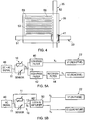
- Fig. 4 schematically illustrates an apparatus 10 according to another embodiment of the disclosure.
- the electrodes 33, 35 may have an interdigitated structure.
- the example illustrated in Fig. 4 is one of many possible arrangements. Other arrangements may include, for example, a parallel plate arrangement or interpenetrating coil arrangement for the electrodes 33, 35.
- the drive electrode 33 and the sense electrode 35 may be provided on a piezo-resistive substrate.
- An environment sensitive layer 37 may be provided between the electrodes 33, 35 and the environment.
- the environment sensitive layer 37 may comprise any suitable material as described above.
- the electrode arrangement illustrated in Fig. 4 comprises a drive electrode 33 and a sense electrode 35.
- the portion of the drive electrode 33 illustrated in Fig. 4 comprises a first elongate portion 51, a second elongate portion 53 and a plurality of third elongate portions 55.
- the second elongate portion 53 extends from the first elongate portion 51 in a direction orthogonal to the first elongate portion 51.
- the plurality of third elongate portions 55 extend from the second elongate portion 53 in a direction orthogonal to the second elongate portion 53 and parallel to the first elongate portion 51.
- the portion of the sense electrode 35 illustrated in Fig. 4 also comprises a first elongate portion 52.
- the first elongate portion 51 of the drive electrode 33 and the first elongate portion 52 extend in orthogonal directions.
- the first elongate portion 51 of the drive electrode 33 and the first elongate portion 52 of the sense electrode 35 are configured to cross over each other.
- a dielectric spacer 41 may be provided between the two electrodes 33, 35 at the point where they cross over to avoid a short circuit.
- a conductive spacer 41 may be provided to form a variable resistive sensor.
- the sense electrode 35 also comprises a plurality of second elongate portions 56.
- the second elongate portions 56 extend from the first elongate portion 52 in a direction orthogonal to the first elongate portion 52.
- the plurality of second portions 56 of the sense electrode 35 may be positioned so that they are located between the plurality of third portions 55 of the drive electrode 33. This may form an interdigitated structure where the layout of the electrodes 33, 35 resembles interlocking fingers. This may enable a capacitive sensor to be formed by the electrodes 33, 35.
- Figs. 5A and 5B illustrate a system comprising a signal generator 46 for providing the input signal 11 to the apparatus 10 and processing circuitry 22 configured to detect a first signal value comprising at least a real component and configured to detect a second signal value comprising at least an imaginary component, wherein the first component and the second component have a known phase off-set.
- the first signal value is typically the real component X o of the output signal 13 and the second value is typically the imaginary component Y o of the output signal 13.
- the signal generator 46 simultaneously provides an input signal 11 that comprises an alternating component and a static component.
- the alternating component may be at a single frequency or a mixture of frequencies.
- the processing circuitry 22 comprises a low-pass filter 40 that filters the output signal 13 blocking the alternating component but allowing the static (dc) component Xo to pass.
- the processing circuitry 22 comprises in parallel to the low-pass filter 40 a high pass filter 42 that filters the output signal 13 blocking the static (dc) component but allowing the alternating (ac) component Y o to pass.
- a rectifier and filter 44 may be used to further process the filtered signal.
- the signal generator 26 provides an input signal 11 that comprises an alternating component only.
- the alternating component may be at a single frequency.
- the processing circuitry 22 comprises a lock-in amplifier 50 that receives the output signal 13 as an input and the input signal 11 as a reference. It produces as a first output, X o , the in-phase component and as a second output, Y o , the quadrature-phase component.
- Analysis circuitry 24 may be configured to analyse the current capacitance and the current resistance for the different cells 36 (located at different areas) to:
- the environmental parameter may include physiological parameters such as the conductivity of the user's skin, the temperature of the user's skin, the humidity of the user's skin or any other property such as the pH of the skin or sweat.
- the analysis may use stored calibration data.
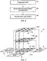
- Fig. 6 illustrates a method of manufacturing an apparatus 10 according to an embodiment.
- the method comprises, at block 61, forming a piezo-resistive substrate 31 configured to have a variable resistance that varies in response to a force applied to the apparatus10.
- the method also comprises, at block 63, mounting a sensor arrangement 12 comprising at least one sensor on the piezo-resistive substrate 31 wherein the sensor is configured to vary an input signal in response to a sensed parameter.
- the sensor arrangement 12 may comprise a plurality of electrodes 33, 35.
- the electrodes 33, 35 may be formed on the piezo-resistive substrate 31 using any suitable technique.
- the method also comprises, at block 65, providing an input configured to receive an input signal 11 comprising a time varying component and providing an output configured to provide an output signal 13 that depends upon the resistance of the piezo-resistive substrate 31 and the parameter sensed by the at least one sensor of the sensor arrangement 12.
- the method may comprise further blocks such as forming a protective layer over the sensor arrangement 12.
- Fig. 7 schematically illustrates an example embodiment which may be used to integrate further sensors into an apparatus 10.
- the apparatus 10 may comprise a plurality of sensor arrangements 12 where each of the sensor arrangements 12 may be provided in a different layer.
- the sensor arrangements 12 may comprise capacitive and/or variable resistance sensors as described above. In some embodiments one or more of the sensor arrangements 12 may comprise a piezo-resistive substrate 31 as described above. However it is to be appreciated that embodiments of the disclosure could be implemented using just capacitive and/or resistive sensors.
- a variable resistance sensor may have a variable resistance that varies with, for example, strain, presence of a specific chemical or biochemical molecule, light, temperature or any other suitable parameter.
- a capacitive sensor may have a capacitance that varies with, for example strain, presence of a specific chemical or biochemical molecule, light, temperature or any other suitable parameter.
- the capacitive sensors may also be configured to detect a user touching or otherwise actuating a surface of the apparatus 10.
- each of the sensor arrangements 12 are provided in a different layer 71.
- the layers 71 may be physically separate or distinct layers.
- Each of the sensor arrangements 12 comprises a plurality of sensors.
- the plurality of sensors 73 are arranged in a grid.
- Each grid comprises a plurality of rows of sensors and a plurality of columns of sensors.
- the rows and columns may be arranged to be orthogonal or substantially orthogonal to each other.
- the layers 71 may be arranged to extend orthogonal to or substantially orthogonal to the rows and columns. In other embodiments other arrangements may be used.
- the apparatus illustrated in Fig. 7 also comprises first selection circuitry 6 and second selection circuitry 8.
- the selection circuitry may comprise a multiplexer.
- the first selection circuitry 6 may be configured to sequence the row to which the input signal 11 is provided through a series of different rows. Each row may be made active once in a period T1 for a time T2.
- the second selection circuitry 8 may be configured to sequence the column from which the output signal 13 is received through a series of different columns. Each column may be made active once in the time period T1.
- the signals may have a regular time sequence, as described above, where each cell is addressed for as frequently and for the same amount of time as all the other cells. In other embodiments the signals may have an irregular time sequence so that some cells are addressed more frequently than others and/or for a longer period of time.
- all of the cells may be active all of the time. In other embodiments some of the cells may only be active and addressed by an input signal for a portion of the time. For example, some cells may only be made active and addressed by an input signal in response to a detected parameter.
- the apparatus 10 may be configured so that the same first selection circuitry 6 and second selection circuitry 8 may be used for each of the different layers 71.
- the apparatus 10 may comprise third selection circuitry 5 which may be configured to switch the first and second selecting circuitry 6, 8 between the respective layers 71. In the example apparatus 10 of Fig. 7 this may be achieved by only activating drive and sense electrodes in a given layer 71 when the gate electrode for that layer 71 is set to be non-zero by the third selection circuitry 5.
- FIG 8 An example sequence of how each of the selection circuitries 6, 8, 5 may address each of the electrodes is illustrated in Fig 8 .
- the apparatus 10 of Fig. 7 may also comprise an input configured to receive an input signal 11 comprising a time varying component and an output configured to provide an output signal 13 that depends on each of the first, second and third sensor arrangements.
- the apparatus 10 of Fig. 7 may also comprise processing circuitry configured to process output signals 13 from different areas of the different sensor arrangement 12 to determine the current capacitance for the different areas and the current resistance for the different areas.
- the apparatus 10 may comprise analysis circuitry configured to analyse the current capacitance and the current resistance for the different areas (cells).
- the processing circuitry and the analysis circuitry may be integrated in a module 20 or they may be provided separately.
- each of the different sensor arrangements may be configured to detect different parameters.
- Fig. 9 schematically illustrates a sensor arrangement 12 which may be provided in one or more of the layers 71 of the apparatus 10 illustrated in Fig. 7 .
- the sensor arrangement 12 comprises a plurality of variable resistance sensors integrated with a plurality of capacitance sensors.
- the sensors are formed by a plurality of drive and sense electrodes 33, 35.
- Each row of the arrangement of Fig. 9 comprises a first plurality of interconnected drive electrodes 33 and each column comprises a second plurality of interconnected sense electrodes 35.
- At least one variable resistor sensor is associated with each row and/or column. In the illustrated example, at least one variable resistor sensor is connected between each row interconnect and each column interconnect, where the rows and column cross, and connected in parallel to a capacitor formed by a drive electrode 33 and a sense electrode 35.
- an in-line transistor 76 is integrated with the drive and sense electrodes 33, 35.
- the transistor 76 may be configured so that when the third selection circuitry 5 selects the gate for the particular layer 71 it turns the transistors for the drive and sense electrodes 33, 35 in that layer 71 to an on state and enables measurements from the sense electrodes 35 to be obtained.
- the third selection circuitry 5 When the third selection circuitry 5 is configured so that the gate for a particular layer is not selected then the transistors for the drive and sense electrodes 33, 35 in that layer are turned to an off state.
- the drive and sense electrodes 33, 35 are connected to ground via a high impedance resistor 78.
- one or more of the layers of sensors may comprise a piezo-resistive substrate 31 as described above.
- Fig 10 illustrates a device 81 which may incorporate the above described sensor arrangements 12.
- the device 81 may comprise a plurality of layers 71 which form a multilayered skin.
- One or more of the layers 71 of the skin may comprise a sensor arrangement 12 as described above.
- the device 81 may be flexible.
- the device 81 may be flexible so that it can be deformed by the user of the device 81 applying a force to the device 81. For example, a user may be able to change the shape of the device 81 by pulling or twisting the device 81.
- the device 81 comprises four layers.
- the first layer 83 may provide an outer surface of the device 81.
- the outer surface may come into direct contact with the environment and a user of the device 81.
- the outermost layer may comprise one or more sensors which may be configured to sense environmental parameters such as air quality, temperature and pressure or any other suitable parameter.
- the second layer 85 may comprise sensors which may be configured to detect touch and/or deformation. Such sensors may comprise a piezo-resistive substrate 31 as described above.
- the third layer 87 may comprise electronic circuitry which may drive the device 81.
- the fourth layer 89 may be configured to form an outer surface which may also be touched by the user of the device 81. This may mean that the fourth layer 89 may be touched by a user of the device 81.
- the fourth layer 89 may comprise one or more sensors which may be configured to respond to physiological parameters of the user, such as skin conductivity, heart rate, body temperature, blood oxygen level or any other suitable parameter.
- Fig. 11 illustrates a method of manufacturing an apparatus 10.
- the example method comprises, at block 91, forming a first sensor arrangement 12A configured in a first layer 71A.
- the method comprises, at block 93, forming a second sensor arrangement 12B configured in a second layer 71B.
- the method also comprises, at block 95, forming a third sensor arrangement 12C configured in a third layer 71C.
- each of the sensor arrangements 12 may be configured to vary an input signal in response to a sensed parameter.
- the method may also comprise providing, at block 97 an input configured to receive an input signal comprising a time varying component and providing an output configured to provide an output signal that depends on each of the first, second and third sensor arrangements 12.
- the method may comprise further blocks such as forming a protective layer over the sensor arrangement 12 or mounting the sensor arrangements 12 on a substrate.
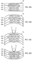
- Figs. 12A to 12D and 13 illustrate an apparatus 10 according to another example of the disclosure.
- the apparatus 10 comprises a first sensor 111 and a second sensor 113.
- the apparatus 10 may be flexible.
- the apparatus 10 may be flexible so that it may be deformed in response to a force and/or pressure applied to the apparatus 10 by a user.
- the force may be applied by a user pulling, bending, flexing or twisting the apparatus 10.
- a force may also be applied by a user making a touch input.
- a touch input may comprise a user pressing, compressing or touching the apparatus 10.
- the apparatus 10 of Figs 12A to 12D and 13 may be configured to determine whether, how and to what degree a device is deformed.
- the apparatus 10 may be configured to enable deformation of the apparatus 10 such as bending, flexing, stretching or twisting to be distinguished from a user making a touch input.
- the apparatus 10 illustrated in Figs. 12A to 12D comprises a first conductive layer 101 and a second conductive layer 103.
- a piezo-resistive layer 105 and a dielectric layer 107 are provided between the first conductive layer 101 and the second conductive layer 103.
- the apparatus 10 may comprise other components.
- the apparatus 10 may comprise additional layers which may be provided overlaying the first conductive layer 101 to control the sensitivity of the apparatus 10.
- the conductive layers 101, 103 may comprise any suitable electrically conductive material.
- the conductive layers 101, 103 may comprise a flexible material.
- the conductive layers 101, 103 may comprise graphene.
- the conductive layers 101, 103 may comprise a graphene based material such as doped graphene or a conductive graphene composite.
- the conductive layers 101, 103 may comprise silver nanowires, carbon nanotubes, ITO, gold, silver, copper, platinum or any other suitable material.
- the two conductive layers 101, 103 may be configured to form a parallel plate capacitor.
- a dielectric layer 107 may be provided between the first conductive layer 101 and the second conductive layer 103.
- the dielectric layer 107 may comprise a flexible material.
- the dielectric layer 107 may comprise an elastomeric material.
- the dielectric layer 107 may be flexible or compressible so that the dielectric layer may be deformed in response to a force and/or pressure applied to the apparatus 10 by a user.
- the apparatus 10 also comprises a piezo-resistive layer 105.
- the piezo-resistive layer 105 may be provided between the first conductive layer 101 and the second conductive layer 103. In the example illustrated in Figs. 12A to 12D the piezo-resistive layer 105 is provided between the first conductive layer 101 and the dielectric layer 107. In some other examples the piezo-resistive layer 105 may be provided between the dielectric layer 107 and the second conductive layer 103.
- the piezo-resistive layer 105 may comprise any material which may be sensitive to a force and/or pressure applied to the apparatus 10.
- the force applied to the apparatus 10 may change the resistance of the piezo-resistive layer 105.
- the piezo-resistive layer 105 may be configured to be sensitive to a force applied by a user pressing or compressing the apparatus 10.
- the piezo-resistive layer 105 may also be configured to be sensitive to other mechanical deformations such as twisting, bending, flexing or stretching.
- the piezo-resistive layer 105 may comprise any suitable material.
- the piezo-resistive layer 105 may comprise force sensitive rubber or any other suitable conductive composites.
- the piezo-resistive layer 105 may comprise a composite of filler particles within an insulating matrix.
- the filler particles may comprise conducting particles and/or semi-conducting particles and/or non-conducting particles.
- the electrical conduction may be based on percolation theory so that as the piezo-resistive layer 105 is stressed the filler particles may come into contact and one or more conduction paths may be formed in the piezo-resistive layer 105.
- the piezo-resistive layer 105 may comprise a quantum tunnelling composite. In such embodiments the electrical conduction is based on electron tunnelling.
- the piezo-resistive layer 105 may have a resistivity which may also be dependent on temperature.
- Fig. 13 illustrates a circuit of the apparatus 10 of Figs. 12A to 12D .
- the piezo-resistive layer 105 may form a variable resistor 111.
- the piezo-resistive layer 105 may form a first sensor.
- the resistance of the variable resistor 111 may depend on the forces applied to the piezo-resistive layer 105. In some examples the resistance of the piezo-resistive layer 105 may decrease so that the piezo-resistive layer 105 becomes more conductive as the piezo-resistive layer 105 is deformed or compressed.
- the first and second conductive layers 101, 103 form a variable capacitor 113.
- the variable capacitor 113 may form a second sensor.
- the capacitance of the variable capacitor 113 may depend on the distance between the two conductive layers 101, 103.
- the distance between the two conductive layers 101, 103 may change as a force and/or pressure is applied to the apparatus as this may cause the deformation and/or compression of the dielectric layer 107 and the piezo-resistive layer 105 provided between the two conductive layers 101, 103.
- the apparatus 10 is configured to receive an input signal 11.
- the input signal 11 may comprise a time varying component.
- the apparatus 10 provides an output signal 13.
- the output signal 13 may depend on the resistance of the piezo-resistive layer 105 and the capacitance of the two conductive layers 101, 103.
- the resistance R of the piezo-resistive layer 105 is connected in electrical series to the capacitance C of the two conductive layers 101, 103.
- Figs. 12A to 12D illustrate the apparatus 10 in four different states of actuation.
- the piezo-resistive layer 105 may be more sensitive to the forces and/or pressure applied to the apparatus 10 than the two conductive layers 101, 103 so that the first sensor has a higher sensitivity than the second sensor. This may enable the output signal 13 provided by the apparatus 10 to be analysed to enable the different types of applied force and states of actuation to be distinguished from each other.
- the two conductive layers 101, 103 may be more sensitive to the forces and/or pressure applied to the apparatus 10 than the piezo-resistive layer.
- the second sensor may have a higher sensitivity than the first sensor.
- the apparatus 10 is configured in a flat or substantially flat configuration.
- the flat configuration may be the neutral or equilibrium configuration of the apparatus 10. It is to be appreciated that in other examples the apparatus 10 may be configured so that the neutral or equilibrium configuration is a curved or bent configuration.
- the apparatus 10 is not deformed by bending, twisting, flexing or stretching and has not been pressed or touched either.
- the piezo-resistive layer 105 may be insulating.
- the output provided by the first and second sensors may indicate that no input has been made.
- the apparatus 10 has been bent into a curved shape but has not been pressed by the user. This has caused deformation of the piezo-resistive layer 105 and so changes the resistance of the piezo-resistive layer 105. This has caused a change in the resistance of the first sensor. The decrease in the resistance may be detected as a decrease in the real component of the impedance of the apparatus 10.
- the apparatus 10 has been bent into a curved shape and pressed by a user.
- the pressing by the user causes further deformation of the first conductive layer and the piezo-resistive layer.
- the pressing by the user may also cause deformation of the dielectric layer 107.
- the pressing of the apparatus 10 in addition to the bending causes further deformation of the piezo-resistive layer 105 which further reduces the resistance of the piezo-resistive layer from the configuration illustrated in Fig. 12B .
- the resistance of the piezo-resistive layer 105 may be lower when the apparatus 10 is bent and pressed (as indicated in Fig. 12C ) than when the apparatus is just bent (as indicated in Fig. 12B ).
- the decrease in the resistance may be detected as a decrease in the real component of the impedance of the apparatus 10.
- the pressing of the apparatus 10 also causes bending of the first conductive layer 101.
- the pressing of the apparatus 10 may also cause compression of the dielectric layer 107. This may decrease the separation of the two conductive layers 101, 103 and so increase the capacitance.
- the increase in capacitance may be detected as a decrease in the magnitude of the imaginary component of the impedance of the apparatus 10.
- the pressing of the apparatus 10 also causes bending of the first conductive layer 101 and may also cause compression of the dielectric layer 107. This may decrease the separation of the two conductive layers 101, 103 and so increase the capacitance.
- the increase in capacitance may be detected as a decrease in the imaginary component of the impedance of the apparatus 10.
- the decrease in the capacitance may be similar to the decrease which is detected when the apparatus 10 is both bent and pressed.
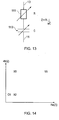
- Fig. 14 is an Argand diagram illustrating an example of an output signal 13 that depends upon both the resistance of the piezo-resistive layer 105 and the capacitance of the two conductive layers 101, 103.
- the values of the impedance Z for each of the actuation states illustrated in Figs. 12A to 12D are indicated on the Argand diagram.
- the impedance of the actuation states indicated in Figs. 12C and 12D may have similar values.
- the output signal 13 may have a real component Re(Z) and an imaginary component Im(Z).
- the imaginary component and the real component have a phase difference of ⁇ /2 radians so the two components are orthogonal (in quadrature).
- the output signal 13 may be processed to determine the real component Re(Z) and the imaginary component Im(Z).
- the output signal 13 may be analysed to determine the real component Re(Z) and the imaginary component Im(Z) to detect changes in the resistance of the piezo-resistive layer 105 and the capacitance of the two conductive layers 101, 103. This may provide information which may be used to differentiate different types of inputs. It may enable deformation of the apparatus 10 due to bending, flexing, twisting and stretching to be distinguished from user inputs such as touching or pressing the apparatus 10.
- Fig. 15 illustrates a method of manufacturing an apparatus 10 as illustrated in Figs. 12A to 12D .
- the first sensor may be formed by forming the piezo-resistive layer 105.
- the second sensor may be formed by forming the two conductive layers 101, 103 and arranging them with the dielectric layer and piezo-resistive layer between.
- the example method of Fig. 15 illustrates an example method which may use a quantum tunnelling composite for the piezo-resistive layer 105.
- the conductive layer may be formed by mounting a conductive material such as graphene onto a polymer such as PEN.
- the PEN/graphene sheet may have a thickness within a range of between about 25 micrometers to 125 micrometers. In other examples a material such as ITO may be used.
- a piezo-resistive material such as a quantum tunnelling composite is attached to a layer of a conductive material such as graphene or a graphene based material.
- the piezo-resistive material may be attached to the conductive material using any suitable process such as screen printing or sandwiching.
- the dielectric layer 107 may be formed from an elastomer such as polydimethylsiloxane (PDMS).
- PDMS polydimethylsiloxane
- the elastomer may be selected to have an appropriate Young's modulus so as to enable the apparatus 10 to have appropriate sensitivity.
- the dielectric layer 107 may have a thickness in the range of from about 250 micrometers to 500 micrometers.
- the dielectric layer 107 may be formed using any suitable technique such as bar coating a polymer solution onto one of the conductive layers. Once the polymer solution has been coated onto the PEN/graphene layer the solution is cured by heating to a suitable temperature for a suitable amount of time. For example, the solution may be cured at 80 degrees Celsius for 1 hour.
- the elastomer solution may also be outgassed to remove any bubbles from the dielectric so as to provide a uniform film.
- the dielectric layer 107 may be formed on the PEN/graphene layer which was formed in block 121. In other examples the dielectric layer 107 may be formed on the piezo-resistive layer which was attached in block 123.
- the two conductive layers may be sandwiched together to form a stack with the elastomer and piezo-resistive layer provided between the two conductive layers.
- the method may comprise further blocks such as forming a protective layer over the sensor arrangement 12 or mounting the sensor arrangements 12 on a substrate.
- connection means operationally coupled and any number or combination of intervening elements can exist (including no intervening elements).
- the analysis circuitry 24 previously described may be implemented using instructions that enable hardware functionality, for example, by using executable computer program instructions in a general-purpose or special-purpose processor that may be stored on a computer readable storage medium (disk, memory etc) to be executed by such a processor.
- a general-purpose or special-purpose processor may be stored on a computer readable storage medium (disk, memory etc) to be executed by such a processor.
- a processor may be configured to read from and write to the memory.
- the processor may also comprise an output interface via which data and/or commands are output by the processor and an input interface via which data and/or commands are input to the processor.
- the memory stores a computer program comprising computer program instructions that control the operation of the apparatus 10 when loaded into the processor.
- the computer program instructions provide the logic and routines that enable the apparatus to perform the methods described.
- the processor by reading the memory is able to load and execute the computer program.
- the apparatus 10 therefore comprises: at least one processor: and at least one memory including computer program code, the at least one memory and the computer program code configured to, with the at least one processor, cause the analysis circuitry to perform as described.
- the computer program may arrive at the apparatus 10 via any suitable delivery mechanism.
- the delivery mechanism may be, for example, a non-transitory computer-readable storage medium, a computer program product, a memory device, a record medium such as a compact disc read-only memory (CD-ROM) or digital versatile disc (DVD), an article of manufacture that tangibly embodies the computer program.
- the delivery mechanism may be a signal configured to reliably transfer the computer program.
- the apparatus 10 may propagate or transmit the computer program as a computer data signal.
- memory is illustrated as a single component it may be implemented as one or more separate components some or all of which may be integrated/removable and/or may provide permanent/semi-permanent/ dynamic/cached storage.
- references to 'computer-readable storage medium', 'computer program product', 'tangibly embodied computer program' etc. or a 'controller', 'computer', 'processor' etc. should be understood to encompass not only computers having different architectures such as single/multi- processor architectures and sequential (Von Neumann)/parallel architectures but also specialized circuits such as field-programmable gate arrays (FPGA), application specific circuits (ASIC), signal processing devices and other processing circuitry.
- References to computer program, instructions, code etc. should be understood to encompass software for a programmable processor or firmware such as, for example, the programmable content of a hardware device whether instructions for a processor, or configuration settings for a fixed-function device, gate array or programmable logic device etc.
- circuitry refers to all of the following:
- circuitry would also cover an implementation of merely a processor (or multiple processors) or portion of a processor and its (or their) accompanying software and/or firmware.
- circuitry would also cover, for example and if applicable to the particular claim element, a baseband integrated circuit or applications processor integrated circuit for a mobile phone or a similar integrated circuit in server, a cellular network device, or other network device.”
- module' refers to a unit or apparatus that excludes certain parts/components that would be added by an end manufacturer or a user.
Claims (14)
- Appareil (10) comprenant :un agencement de capteur résistif (111) dans une première couche ;un agencement de capteur capacitif (113) dans une seconde couche ;dans lequel les agencements de capteur résistif (111) et capacitif (113) sont configurés pour faire varier un signal d'entrée (11) en réponse à des premier et second paramètres détectés respectifs, etdans lequel l'appareil (10) comprend également un ensemble de circuits d'entrée configuré pour fournir un signal d'entrée (11) et un ensemble de circuits de sortie configuré pour détecter un signal de sortie (13) comprenant des composantes réelle (X0) et imaginaire (Y0) d'une impédance complexe (Z), la composante réelle (X0) indiquant un changement de résistance (R) provoqué par le premier paramètre détecté et la composante imaginaire (Y0) indiquant un changement de capacité (C) provoqué par le second paramètre détecté.
- Appareil (10) selon la revendication 1, dans lequel le premier paramètre détecté comprend une déformation de l'appareil (10) et le second paramètre détecté comprend une entrée tactile, une déformation de l'appareil (10) comprenant un pliage et/ou un étirement et/ou une torsion de l'appareil (10), l'entrée tactile comprenant une compression de l'appareil (10).
- Appareil (10) selon la revendication 1 ou 2, dans lequel l'appareil (10) comprend au moins une couche de non-détection (47).
- Appareil (10) selon l'une quelconque des revendications précédentes, dans lequel le signal d'entrée (11) comprend un composant variant dans le temps.
- Appareil (10) selon l'une quelconque des revendications précédentes, comprenant en outre :un premier ensemble de circuits de sélection (5) configuré pour fournir de manière sélective le signal d'entrée (11) aux différents agencements de capteur sélectionnés (12A à 12C) ;un deuxième ensemble de circuits de sélection (6) configuré pour fournir de manière sélective le signal d'entrée à une première partie (D1) de l'agencement de capteur sélectionné (12C) ; etun troisième ensemble de circuits de sélection (8) configuré pour recevoir de manière sélective le signal de sortie (13) en provenance d'une seconde partie (S1) de l'agencement de capteur sélectionné (12C).
- Appareil (10) selon la revendication 5, dans lequel le deuxième ensemble de circuits de sélection (6) est configuré pour mettre en séquence la première partie (D1) à laquelle le signal d'entrée (11) est fourni au moyen d'une série de différentes premières parties (D1 à D3) de l'agencement de capteur sélectionné (12C) et le troisième ensemble de circuits de sélection (8) est configuré pour mettre en séquence la seconde partie (S1) en provenance de laquelle le signal de sortie (13) est reçu au moyen d'une série de différentes secondes parties (S1 à S3) de l'agencement de capteur sélectionné (12C).
- Appareil (10) selon la revendication 5, dans lequel les premières parties (D1 à D3) de l'agencement de capteur sélectionné (12C) sont parallèles à une première direction, les secondes parties (S1 à S3) de l'agencement de capteur sélectionné (12C) sont parallèles à une seconde direction et les première et seconde directions sont orthogonales.
- Appareil (10) selon l'une quelconque des revendications précédentes, comprenant en outre :un ensemble de circuits (22) configuré pour traiter des signaux de sortie (13) provenant de différents zones (36) des agencements de capteur (12) ; etun ensemble de circuits d'analyse (24) configuré pour détecter des changements de capacité (C) et de résistance (R) pour les différentes zones (36).
- Appareil (10) selon l'une quelconque des revendications précédentes, dans lequel l'agencement de capteur capacitif (113) est formé sur un substrat (31) qui forme l'agencement de capteur résistif (111).
- Appareil (10) selon la revendication 9, dans lequel le substrat (31) comprend un substrat piézorésistif.
- Appareil (10) selon l'une quelconque des revendications précédentes, dans lequel l'agencement de capteur capacitif (113) comprend des première (43) et seconde (45) couches conductrices séparées par une couche diélectrique (41).
- Procédé de fabrication d'un appareil (10) comprenant :la formation d'un agencement de capteur résistif (111) dans une première couche ;la formation d'un agencement de capteur capacitif (113) dans une seconde couche, dans lequel les agencements de capteur (111, 113) sont configurés pour faire varier un signal d'entrée (11) en réponse à des premier et second paramètres détectés respectifs ;la fourniture d'un ensemble de circuits d'entrée configuré pour fournir le signal d'entrée (11) ; etla fourniture d'un ensemble de circuits de sortie configuré pour détecter un signal de sortie (13) comprenant des composantes réelle (X0) et imaginaire (Y0) d'une impédance complexe (Z), la composante réelle (X0) indiquant un changement de résistance (R) provoqué par le premier paramètre détecté et la composante imaginaire (Y0) indiquant un changement de capacité (C) provoqué par le second paramètre détecté.
- Procédé selon la revendication 12, dans lequel l'agencement de capteur capacitif (113) est formé sur un substrat (31) qui forme l'agencement de capteur résistif (111) .
- Procédé selon la revendication 13, dans lequel le substrat (31) comprend un substrat piézorésistif.
Applications Claiming Priority (2)
| Application Number | Priority Date | Filing Date | Title |
|---|---|---|---|
| US13/548,702 US8893565B2 (en) | 2012-07-13 | 2012-07-13 | Apparatus for sensing |
| PCT/IB2012/056925 WO2014009781A1 (fr) | 2012-07-13 | 2012-12-03 | Appareil pour détection |
Publications (3)
| Publication Number | Publication Date |
|---|---|
| EP2872976A1 EP2872976A1 (fr) | 2015-05-20 |
| EP2872976A4 EP2872976A4 (fr) | 2016-04-13 |
| EP2872976B1 true EP2872976B1 (fr) | 2019-10-02 |
Family
ID=49912785
Family Applications (1)
| Application Number | Title | Priority Date | Filing Date |
|---|---|---|---|
| EP12880730.2A Active EP2872976B1 (fr) | 2012-07-13 | 2012-12-03 | Appareil pour détection |
Country Status (6)
| Country | Link |
|---|---|
| US (1) | US8893565B2 (fr) |
| EP (1) | EP2872976B1 (fr) |
| JP (1) | JP6062047B2 (fr) |
| KR (2) | KR101864560B1 (fr) |
| CN (1) | CN105051658B (fr) |
| WO (1) | WO2014009781A1 (fr) |
Families Citing this family (52)
| Publication number | Priority date | Publication date | Assignee | Title |
|---|---|---|---|---|
| TWI398800B (zh) * | 2009-08-14 | 2013-06-11 | Htc Corp | 觸控面板及其輸出方法 |
| WO2011047171A2 (fr) | 2009-10-16 | 2011-04-21 | Kesumo, Llc | Pédale de contrôle |
| US9076419B2 (en) | 2012-03-14 | 2015-07-07 | Bebop Sensors, Inc. | Multi-touch pad controller |
| GB2525174A (en) * | 2014-04-14 | 2015-10-21 | Nokia Technologies Oy | An apparatus and method for sensing |
| US9753568B2 (en) * | 2014-05-15 | 2017-09-05 | Bebop Sensors, Inc. | Flexible sensors and applications |
| US9965076B2 (en) * | 2014-05-15 | 2018-05-08 | Bebop Sensors, Inc. | Piezoresistive sensors and applications |
| US9442614B2 (en) * | 2014-05-15 | 2016-09-13 | Bebop Sensors, Inc. | Two-dimensional sensor arrays |
| US10362989B2 (en) | 2014-06-09 | 2019-07-30 | Bebop Sensors, Inc. | Sensor system integrated with a glove |
| EP2980727B1 (fr) | 2014-08-01 | 2019-06-26 | Nokia Technologies OY | Appareils et procédés permettant à des informations d'être lues à partir d'un appareil à écran tactile |
| EP2980569B1 (fr) * | 2014-08-01 | 2020-09-23 | Nokia Technologies Oy | Appareil et procédé pour détecter un paramètre |
| DE112015004929T5 (de) * | 2014-10-30 | 2017-07-13 | Bebop Sensors, Inc. | In einem Handschuh integriertes Sensorsystem |
| GB2533667B (en) | 2014-12-23 | 2017-07-19 | Cambridge Touch Tech Ltd | Pressure-sensitive touch panel |
| CN107209590B (zh) | 2014-12-23 | 2021-10-15 | 剑桥触控科技有限公司 | 压敏触摸面板 |
| CN105807144B (zh) | 2014-12-31 | 2019-01-18 | 清华大学 | 静电计 |
| CN105807970B (zh) * | 2014-12-31 | 2018-08-17 | 清华大学 | 悬停控制装置 |
| CN105807974B (zh) * | 2014-12-31 | 2018-09-11 | 清华大学 | 触摸和悬停感测装置 |
| CN105807975B (zh) * | 2014-12-31 | 2019-01-18 | 清华大学 | 悬停控制装置 |
| CN105808030B (zh) * | 2014-12-31 | 2018-10-02 | 清华大学 | 静电传感器 |
| CN105807146B (zh) | 2014-12-31 | 2018-10-02 | 清华大学 | 静电分布测量装置 |
| CN105807973B (zh) * | 2014-12-31 | 2019-01-18 | 清华大学 | 静电传感器 |
| CN105807971B (zh) * | 2014-12-31 | 2019-01-18 | 清华大学 | 静电传感器 |
| CN105807976B (zh) * | 2014-12-31 | 2019-02-12 | 清华大学 | 静电传感器 |
| CN105808031B (zh) * | 2014-12-31 | 2019-01-18 | 清华大学 | 静电感测方法 |
| CN105807145B (zh) | 2014-12-31 | 2019-01-18 | 清华大学 | 静电计 |
| CN105807977B (zh) * | 2014-12-31 | 2019-02-12 | 清华大学 | 触摸和悬停感测装置 |
| EP3054597B1 (fr) * | 2015-02-09 | 2020-04-15 | Nokia Technologies Oy | Appareil et procédés de détection |
| US9863823B2 (en) | 2015-02-27 | 2018-01-09 | Bebop Sensors, Inc. | Sensor systems integrated with footwear |
| US10082381B2 (en) | 2015-04-30 | 2018-09-25 | Bebop Sensors, Inc. | Sensor systems integrated with vehicle tires |
| US9827996B2 (en) | 2015-06-25 | 2017-11-28 | Bebop Sensors, Inc. | Sensor systems integrated with steering wheels |
| BR112018002219A2 (pt) * | 2015-08-02 | 2018-09-04 | G Medical Innovations Holdings Ltd | sistema para monitorar sinais vitais |
| CN105138181A (zh) * | 2015-09-23 | 2015-12-09 | 深圳信炜科技有限公司 | 电容式传感器、电容式传感装置和电子设备 |
| US10282046B2 (en) | 2015-12-23 | 2019-05-07 | Cambridge Touch Technologies Ltd. | Pressure-sensitive touch panel |
| GB2544353B (en) | 2015-12-23 | 2018-02-21 | Cambridge Touch Tech Ltd | Pressure-sensitive touch panel |
| KR102456154B1 (ko) * | 2016-01-29 | 2022-10-19 | 삼성디스플레이 주식회사 | 센서, 터치 센서 및 표시 장치 |
| JP6297613B2 (ja) * | 2016-03-22 | 2018-03-20 | Nissha株式会社 | 感圧センサ |
| KR101904969B1 (ko) | 2016-07-29 | 2018-10-10 | 삼성디스플레이 주식회사 | 표시장치 |
| US10836639B1 (en) | 2016-10-26 | 2020-11-17 | Air Stations Llc/Elevated Analytics Llc Joint Venture | Air quality measurement system |
| US10866226B1 (en) | 2017-02-07 | 2020-12-15 | Air Stations Llc/Elevated Analytics Llc Joint Venture | Multi-point ground emission source sensor system |
| US10928371B1 (en) | 2017-03-31 | 2021-02-23 | Air Stations Llc/Elevated Analytics Llc Joint Venture | Hand-held sensor and monitor system |
| US11093088B2 (en) | 2017-08-08 | 2021-08-17 | Cambridge Touch Technologies Ltd. | Device for processing signals from a pressure-sensing touch panel |
| GB2565305A (en) | 2017-08-08 | 2019-02-13 | Cambridge Touch Tech Ltd | Device for processing signals from a pressure-sensing touch panel |
| GB2568217A (en) | 2017-08-08 | 2019-05-15 | Cambridge Touch Tech Ltd | Touch panel pressure detection |
| CN107607031A (zh) * | 2017-10-17 | 2018-01-19 | 广州中国科学院工业技术研究院 | 网状传感器及测量方法 |
| KR102510459B1 (ko) | 2017-12-12 | 2023-03-17 | 삼성디스플레이 주식회사 | 표시 장치 |
| US10119869B1 (en) * | 2017-12-21 | 2018-11-06 | Tactotek Oy | Method for manufacturing a strain gauge device, a strain gauge device, and the use of the device |
| CN112203581A (zh) * | 2018-05-30 | 2021-01-08 | 美梦有限公司 | 监测方法和缓冲结构 |
| US10884496B2 (en) | 2018-07-05 | 2021-01-05 | Bebop Sensors, Inc. | One-size-fits-all data glove |
| US11480481B2 (en) | 2019-03-13 | 2022-10-25 | Bebop Sensors, Inc. | Alignment mechanisms sensor systems employing piezoresistive materials |
| US11668686B1 (en) * | 2019-06-17 | 2023-06-06 | Flex Ltd. | Batteryless architecture for color detection in smart labels |
| JP2021004788A (ja) * | 2019-06-26 | 2021-01-14 | 株式会社デンソー | センサ装置 |
| CN110595647B (zh) * | 2019-09-09 | 2021-07-27 | 中南大学 | 一种多功能柔性应变-压力传感器及制备方法 |
| US11749075B2 (en) * | 2021-04-07 | 2023-09-05 | Electronics And Telecommunications Research Institute | Telehaptic device |
Family Cites Families (30)
| Publication number | Priority date | Publication date | Assignee | Title |
|---|---|---|---|---|
| US6578436B1 (en) | 2000-05-16 | 2003-06-17 | Fidelica Microsystems, Inc. | Method and apparatus for pressure sensing |
| US6995752B2 (en) * | 2001-11-08 | 2006-02-07 | Koninklijke Philips Electronics N.V. | Multi-point touch pad |
| GB0407366D0 (en) * | 2004-03-31 | 2004-05-05 | Koninkl Philips Electronics Nv | Textile form touch sensor |
| JP2006039795A (ja) * | 2004-07-26 | 2006-02-09 | Matsushita Electric Ind Co Ltd | 入力装置 |
| US7430925B2 (en) | 2005-05-18 | 2008-10-07 | Pressure Profile Systems, Inc. | Hybrid tactile sensor |
| GB2428306B (en) | 2005-07-08 | 2007-09-26 | Harald Philipp | Two-dimensional capacitive position sensor |
| DE102006000637A1 (de) * | 2006-01-03 | 2007-07-05 | Robert Bosch Gmbh | Anzeigevorrichtung mit Berührung sensitiver Oberfläche |
| US20080048996A1 (en) | 2006-08-11 | 2008-02-28 | Unidym, Inc. | Touch screen devices employing nanostructure networks |
| US20080121045A1 (en) | 2006-11-29 | 2008-05-29 | Cole Matthew C | Multiplexed sensor array |
| EP2026178A1 (fr) * | 2007-08-10 | 2009-02-18 | IEE INTERNATIONAL ELECTRONICS & ENGINEERING S.A. | Pavé tactile à entrées en forme de bande |
| EP2026179A1 (fr) | 2007-08-10 | 2009-02-18 | IEE International Electronics & Engineering S.A.R.L. | Procédé pour la génération de données d'entrée |
| US8421483B2 (en) * | 2008-06-13 | 2013-04-16 | Sony Ericsson Mobile Communications Ab | Touch and force sensing for input devices |
| CN201247458Y (zh) * | 2008-09-04 | 2009-05-27 | 汉王科技股份有限公司 | 一种具有双模式输入功能的显示装置 |
| KR20100065418A (ko) * | 2008-12-08 | 2010-06-17 | 삼성전자주식회사 | 가요성 표시부를 가지는 단말기 및 그의 데이터 표시 방법 |
| KR100980447B1 (ko) | 2008-12-09 | 2010-09-07 | 한국과학기술연구원 | 압전 기판을 이용한 투명 터치 패널 및 그 제조 방법 |
| US8334635B2 (en) * | 2009-06-24 | 2012-12-18 | Ethicon Endo-Surgery, Inc. | Transducer arrangements for ultrasonic surgical instruments |
| EP2275805A1 (fr) * | 2009-07-16 | 2011-01-19 | Acreo AB | Capteur d'humidité |
| TWI398800B (zh) * | 2009-08-14 | 2013-06-11 | Htc Corp | 觸控面板及其輸出方法 |
| US8179376B2 (en) * | 2009-08-27 | 2012-05-15 | Research In Motion Limited | Touch-sensitive display with capacitive and resistive touch sensors and method of control |
| JP5363393B2 (ja) * | 2010-03-30 | 2013-12-11 | オリンパス株式会社 | 可変分光素子 |
| JP5442519B2 (ja) * | 2010-04-07 | 2014-03-12 | ダイキン工業株式会社 | 透明圧電シート、それをそれぞれ含有するフレーム付透明圧電シート、タッチ位置検出用タッチパネル、ディスプレイ装置、タッチパネルおよび電子機器 |
| KR101084782B1 (ko) * | 2010-05-06 | 2011-11-21 | 삼성전기주식회사 | 터치스크린 장치 |
| EP2569687A2 (fr) * | 2010-05-14 | 2013-03-20 | Elo Touch Solutions, Inc. | Système et procédé pour détecter des emplacements de touchers sur un capteur tactile |
| JP2012003522A (ja) * | 2010-06-17 | 2012-01-05 | Panasonic Corp | タッチパネル |
| US8599165B2 (en) | 2010-08-16 | 2013-12-03 | Perceptive Pixel Inc. | Force and true capacitive touch measurement techniques for capacitive touch sensors |
| JP2012043275A (ja) * | 2010-08-20 | 2012-03-01 | Alps Electric Co Ltd | 静電容量式の入力装置 |
| KR20140037011A (ko) | 2010-10-20 | 2014-03-26 | 택투스 테크놀로지, 아이엔씨. | 사용자 인터페이스 시스템 |
| TWM417607U (en) | 2011-02-15 | 2011-12-01 | Howay Corp | Touch panel device with dual sensing interface |
| US8780074B2 (en) | 2011-07-06 | 2014-07-15 | Sharp Kabushiki Kaisha | Dual-function transducer for a touch panel |
| CN102339166A (zh) | 2011-10-12 | 2012-02-01 | 清华大学 | 可折叠、可柔性变形的压电触摸屏 |
-
2012
- 2012-07-13 US US13/548,702 patent/US8893565B2/en active Active
- 2012-12-03 KR KR1020177022585A patent/KR101864560B1/ko active IP Right Grant
- 2012-12-03 EP EP12880730.2A patent/EP2872976B1/fr active Active
- 2012-12-03 WO PCT/IB2012/056925 patent/WO2014009781A1/fr active Application Filing
- 2012-12-03 JP JP2015521078A patent/JP6062047B2/ja active Active
- 2012-12-03 KR KR20157003766A patent/KR20150036576A/ko not_active Application Discontinuation
- 2012-12-03 CN CN201280075762.7A patent/CN105051658B/zh active Active
Non-Patent Citations (1)
| Title |
|---|
| ANONYMOUS: "Complex Impedance", 21 March 2012 (2012-03-21), XP055375050, Retrieved from the Internet <URL:http://web.archive.org/web/20120321175556/http://hyperphysics.phy-astr.gsu.edu/hbase/electric/impcom.html> [retrieved on 20170522] * |
Also Published As
| Publication number | Publication date |
|---|---|
| JP6062047B2 (ja) | 2017-01-18 |
| KR20170097230A (ko) | 2017-08-25 |
| CN105051658B (zh) | 2018-05-29 |
| KR20150036576A (ko) | 2015-04-07 |
| WO2014009781A1 (fr) | 2014-01-16 |
| US8893565B2 (en) | 2014-11-25 |
| JP2015522197A (ja) | 2015-08-03 |
| EP2872976A1 (fr) | 2015-05-20 |
| KR101864560B1 (ko) | 2018-06-04 |
| CN105051658A (zh) | 2015-11-11 |
| EP2872976A4 (fr) | 2016-04-13 |
| US20140013865A1 (en) | 2014-01-16 |
Similar Documents
| Publication | Publication Date | Title |
|---|---|---|
| EP2872976B1 (fr) | Appareil pour détection | |
| EP2820514B1 (fr) | Capteur capacitif et résistif | |
| US10724908B2 (en) | Flexible transparent sensor with ionically-conductive material | |
| TWI582668B (zh) | 觸壓式三維信號輸入裝置、多功能觸控面板及其偵測方法 | |
| EP2544081B1 (fr) | Capteur de détection de position, dispositif de détection de position et procédé de détection de position | |
| US8607651B2 (en) | Hybrid capacitive force sensors | |
| EP2598973B1 (fr) | Système de rendu d'écran tactile et son procédé de fonctionnement | |
| US9366708B2 (en) | Apparatus comprising a flexible substrate and a component supported by the flexible substrate | |
| US8184106B2 (en) | Position detection device | |
| CN107710116B (zh) | 显示一体型输入装置 | |
| TWI530672B (zh) | Input device and input device control method | |
| US10534468B2 (en) | Force sensing using touch sensors | |
| JP2023051944A (ja) | 静電容量型検知センサ、静電容量型検知センサモジュールおよび静電容量型検知センサを用いた状態判定方法 | |
| KR101839216B1 (ko) | 상호정전용량 기반의 터치센서 및 제조방법 | |
| US20240072800A1 (en) | Sensing device | |
| CN114450560B (en) | Capacitive sensor, capacitive sensor module, and state determination method using capacitive sensor | |
| GB2602973A (en) | A deformable sensing layer and methods |
Legal Events
| Date | Code | Title | Description |
|---|---|---|---|
| PUAI | Public reference made under article 153(3) epc to a published international application that has entered the european phase |
Free format text: ORIGINAL CODE: 0009012 |
|
| 17P | Request for examination filed |
Effective date: 20150202 |
|
| AK | Designated contracting states |
Kind code of ref document: A1 Designated state(s): AL AT BE BG CH CY CZ DE DK EE ES FI FR GB GR HR HU IE IS IT LI LT LU LV MC MK MT NL NO PL PT RO RS SE SI SK SM TR |
|
| AX | Request for extension of the european patent |
Extension state: BA ME |
|
| RAP1 | Party data changed (applicant data changed or rights of an application transferred) |
Owner name: NOKIA TECHNOLOGIES OY |
|
| DAX | Request for extension of the european patent (deleted) | ||
| RA4 | Supplementary search report drawn up and despatched (corrected) |
Effective date: 20160310 |
|
| RIC1 | Information provided on ipc code assigned before grant |
Ipc: G06F 3/045 20060101ALI20160304BHEP Ipc: G06F 3/044 20060101AFI20160304BHEP Ipc: G06F 3/041 20060101ALI20160304BHEP |
|
| STAA | Information on the status of an ep patent application or granted ep patent |
Free format text: STATUS: EXAMINATION IS IN PROGRESS |
|
| 17Q | First examination report despatched |
Effective date: 20170529 |
|
| REG | Reference to a national code |
Ref country code: DE Ref legal event code: R079 Ref document number: 602012064631 Country of ref document: DE Free format text: PREVIOUS MAIN CLASS: G06F0003044000 Ipc: G01D0005120000 |
|
| GRAP | Despatch of communication of intention to grant a patent |
Free format text: ORIGINAL CODE: EPIDOSNIGR1 |
|
| STAA | Information on the status of an ep patent application or granted ep patent |
Free format text: STATUS: GRANT OF PATENT IS INTENDED |
|
| INTG | Intention to grant announced |
Effective date: 20190423 |
|
| RIC1 | Information provided on ipc code assigned before grant |
Ipc: G06F 1/16 20060101ALI20190408BHEP Ipc: G01D 5/12 20060101AFI20190408BHEP Ipc: G06F 3/041 20060101ALI20190408BHEP Ipc: G01L 1/20 20060101ALI20190408BHEP Ipc: G01L 1/18 20060101ALI20190408BHEP Ipc: G01L 1/14 20060101ALI20190408BHEP |
|
| GRAS | Grant fee paid |
Free format text: ORIGINAL CODE: EPIDOSNIGR3 |
|
| GRAA | (expected) grant |
Free format text: ORIGINAL CODE: 0009210 |
|
| STAA | Information on the status of an ep patent application or granted ep patent |
Free format text: STATUS: THE PATENT HAS BEEN GRANTED |
|
| RAP1 | Party data changed (applicant data changed or rights of an application transferred) |
Owner name: NOKIA TECHNOLOGIES OY |
|
| AK | Designated contracting states |
Kind code of ref document: B1 Designated state(s): AL AT BE BG CH CY CZ DE DK EE ES FI FR GB GR HR HU IE IS IT LI LT LU LV MC MK MT NL NO PL PT RO RS SE SI SK SM TR |
|
| REG | Reference to a national code |
Ref country code: GB Ref legal event code: FG4D |
|
| REG | Reference to a national code |
Ref country code: CH Ref legal event code: EP Ref country code: AT Ref legal event code: REF Ref document number: 1186690 Country of ref document: AT Kind code of ref document: T Effective date: 20191015 |
|
| REG | Reference to a national code |
Ref country code: DE Ref legal event code: R096 Ref document number: 602012064631 Country of ref document: DE |
|
| REG | Reference to a national code |
Ref country code: IE Ref legal event code: FG4D |
|
| REG | Reference to a national code |
Ref country code: NL Ref legal event code: MP Effective date: 20191002 |
|
| REG | Reference to a national code |
Ref country code: LT Ref legal event code: MG4D |
|
| REG | Reference to a national code |
Ref country code: AT Ref legal event code: MK05 Ref document number: 1186690 Country of ref document: AT Kind code of ref document: T Effective date: 20191002 |
|
| PG25 | Lapsed in a contracting state [announced via postgrant information from national office to epo] |
Ref country code: LT Free format text: LAPSE BECAUSE OF FAILURE TO SUBMIT A TRANSLATION OF THE DESCRIPTION OR TO PAY THE FEE WITHIN THE PRESCRIBED TIME-LIMIT Effective date: 20191002 Ref country code: NO Free format text: LAPSE BECAUSE OF FAILURE TO SUBMIT A TRANSLATION OF THE DESCRIPTION OR TO PAY THE FEE WITHIN THE PRESCRIBED TIME-LIMIT Effective date: 20200102 Ref country code: AT Free format text: LAPSE BECAUSE OF FAILURE TO SUBMIT A TRANSLATION OF THE DESCRIPTION OR TO PAY THE FEE WITHIN THE PRESCRIBED TIME-LIMIT Effective date: 20191002 Ref country code: GR Free format text: LAPSE BECAUSE OF FAILURE TO SUBMIT A TRANSLATION OF THE DESCRIPTION OR TO PAY THE FEE WITHIN THE PRESCRIBED TIME-LIMIT Effective date: 20200103 Ref country code: PL Free format text: LAPSE BECAUSE OF FAILURE TO SUBMIT A TRANSLATION OF THE DESCRIPTION OR TO PAY THE FEE WITHIN THE PRESCRIBED TIME-LIMIT Effective date: 20191002 Ref country code: ES Free format text: LAPSE BECAUSE OF FAILURE TO SUBMIT A TRANSLATION OF THE DESCRIPTION OR TO PAY THE FEE WITHIN THE PRESCRIBED TIME-LIMIT Effective date: 20191002 Ref country code: NL Free format text: LAPSE BECAUSE OF FAILURE TO SUBMIT A TRANSLATION OF THE DESCRIPTION OR TO PAY THE FEE WITHIN THE PRESCRIBED TIME-LIMIT Effective date: 20191002 Ref country code: FI Free format text: LAPSE BECAUSE OF FAILURE TO SUBMIT A TRANSLATION OF THE DESCRIPTION OR TO PAY THE FEE WITHIN THE PRESCRIBED TIME-LIMIT Effective date: 20191002 Ref country code: BG Free format text: LAPSE BECAUSE OF FAILURE TO SUBMIT A TRANSLATION OF THE DESCRIPTION OR TO PAY THE FEE WITHIN THE PRESCRIBED TIME-LIMIT Effective date: 20200102 Ref country code: PT Free format text: LAPSE BECAUSE OF FAILURE TO SUBMIT A TRANSLATION OF THE DESCRIPTION OR TO PAY THE FEE WITHIN THE PRESCRIBED TIME-LIMIT Effective date: 20200203 Ref country code: SE Free format text: LAPSE BECAUSE OF FAILURE TO SUBMIT A TRANSLATION OF THE DESCRIPTION OR TO PAY THE FEE WITHIN THE PRESCRIBED TIME-LIMIT Effective date: 20191002 Ref country code: LV Free format text: LAPSE BECAUSE OF FAILURE TO SUBMIT A TRANSLATION OF THE DESCRIPTION OR TO PAY THE FEE WITHIN THE PRESCRIBED TIME-LIMIT Effective date: 20191002 |
|
| PG25 | Lapsed in a contracting state [announced via postgrant information from national office to epo] |
Ref country code: HR Free format text: LAPSE BECAUSE OF FAILURE TO SUBMIT A TRANSLATION OF THE DESCRIPTION OR TO PAY THE FEE WITHIN THE PRESCRIBED TIME-LIMIT Effective date: 20191002 Ref country code: IS Free format text: LAPSE BECAUSE OF FAILURE TO SUBMIT A TRANSLATION OF THE DESCRIPTION OR TO PAY THE FEE WITHIN THE PRESCRIBED TIME-LIMIT Effective date: 20200224 Ref country code: RS Free format text: LAPSE BECAUSE OF FAILURE TO SUBMIT A TRANSLATION OF THE DESCRIPTION OR TO PAY THE FEE WITHIN THE PRESCRIBED TIME-LIMIT Effective date: 20191002 Ref country code: CZ Free format text: LAPSE BECAUSE OF FAILURE TO SUBMIT A TRANSLATION OF THE DESCRIPTION OR TO PAY THE FEE WITHIN THE PRESCRIBED TIME-LIMIT Effective date: 20191002 |
|
| PG25 | Lapsed in a contracting state [announced via postgrant information from national office to epo] |
Ref country code: AL Free format text: LAPSE BECAUSE OF FAILURE TO SUBMIT A TRANSLATION OF THE DESCRIPTION OR TO PAY THE FEE WITHIN THE PRESCRIBED TIME-LIMIT Effective date: 20191002 |
|
| REG | Reference to a national code |
Ref country code: DE Ref legal event code: R097 Ref document number: 602012064631 Country of ref document: DE |
|
| PG2D | Information on lapse in contracting state deleted |
Ref country code: IS |
|
| PG25 | Lapsed in a contracting state [announced via postgrant information from national office to epo] |
Ref country code: EE Free format text: LAPSE BECAUSE OF FAILURE TO SUBMIT A TRANSLATION OF THE DESCRIPTION OR TO PAY THE FEE WITHIN THE PRESCRIBED TIME-LIMIT Effective date: 20191002 Ref country code: DK Free format text: LAPSE BECAUSE OF FAILURE TO SUBMIT A TRANSLATION OF THE DESCRIPTION OR TO PAY THE FEE WITHIN THE PRESCRIBED TIME-LIMIT Effective date: 20191002 Ref country code: RO Free format text: LAPSE BECAUSE OF FAILURE TO SUBMIT A TRANSLATION OF THE DESCRIPTION OR TO PAY THE FEE WITHIN THE PRESCRIBED TIME-LIMIT Effective date: 20191002 Ref country code: IS Free format text: LAPSE BECAUSE OF FAILURE TO SUBMIT A TRANSLATION OF THE DESCRIPTION OR TO PAY THE FEE WITHIN THE PRESCRIBED TIME-LIMIT Effective date: 20200202 |
|
| REG | Reference to a national code |
Ref country code: CH Ref legal event code: PL |
|
| PLBE | No opposition filed within time limit |
Free format text: ORIGINAL CODE: 0009261 |
|
| STAA | Information on the status of an ep patent application or granted ep patent |
Free format text: STATUS: NO OPPOSITION FILED WITHIN TIME LIMIT |
|
| REG | Reference to a national code |
Ref country code: BE Ref legal event code: MM Effective date: 20191231 |
|
| PG25 | Lapsed in a contracting state [announced via postgrant information from national office to epo] |
Ref country code: IT Free format text: LAPSE BECAUSE OF FAILURE TO SUBMIT A TRANSLATION OF THE DESCRIPTION OR TO PAY THE FEE WITHIN THE PRESCRIBED TIME-LIMIT Effective date: 20191002 Ref country code: SK Free format text: LAPSE BECAUSE OF FAILURE TO SUBMIT A TRANSLATION OF THE DESCRIPTION OR TO PAY THE FEE WITHIN THE PRESCRIBED TIME-LIMIT Effective date: 20191002 Ref country code: MC Free format text: LAPSE BECAUSE OF FAILURE TO SUBMIT A TRANSLATION OF THE DESCRIPTION OR TO PAY THE FEE WITHIN THE PRESCRIBED TIME-LIMIT Effective date: 20191002 Ref country code: SM Free format text: LAPSE BECAUSE OF FAILURE TO SUBMIT A TRANSLATION OF THE DESCRIPTION OR TO PAY THE FEE WITHIN THE PRESCRIBED TIME-LIMIT Effective date: 20191002 |
|
| 26N | No opposition filed |
Effective date: 20200703 |
|
| GBPC | Gb: european patent ceased through non-payment of renewal fee |
Effective date: 20200102 |
|
| PG25 | Lapsed in a contracting state [announced via postgrant information from national office to epo] |
Ref country code: GB Free format text: LAPSE BECAUSE OF NON-PAYMENT OF DUE FEES Effective date: 20200102 Ref country code: LU Free format text: LAPSE BECAUSE OF NON-PAYMENT OF DUE FEES Effective date: 20191203 Ref country code: IE Free format text: LAPSE BECAUSE OF NON-PAYMENT OF DUE FEES Effective date: 20191203 Ref country code: FR Free format text: LAPSE BECAUSE OF NON-PAYMENT OF DUE FEES Effective date: 20191231 |
|
| PG25 | Lapsed in a contracting state [announced via postgrant information from national office to epo] |
Ref country code: SI Free format text: LAPSE BECAUSE OF FAILURE TO SUBMIT A TRANSLATION OF THE DESCRIPTION OR TO PAY THE FEE WITHIN THE PRESCRIBED TIME-LIMIT Effective date: 20191002 Ref country code: CH Free format text: LAPSE BECAUSE OF NON-PAYMENT OF DUE FEES Effective date: 20191231 Ref country code: LI Free format text: LAPSE BECAUSE OF NON-PAYMENT OF DUE FEES Effective date: 20191231 Ref country code: BE Free format text: LAPSE BECAUSE OF NON-PAYMENT OF DUE FEES Effective date: 20191231 |
|
| PG25 | Lapsed in a contracting state [announced via postgrant information from national office to epo] |
Ref country code: CY Free format text: LAPSE BECAUSE OF FAILURE TO SUBMIT A TRANSLATION OF THE DESCRIPTION OR TO PAY THE FEE WITHIN THE PRESCRIBED TIME-LIMIT Effective date: 20191002 |
|
| PG25 | Lapsed in a contracting state [announced via postgrant information from national office to epo] |
Ref country code: MT Free format text: LAPSE BECAUSE OF FAILURE TO SUBMIT A TRANSLATION OF THE DESCRIPTION OR TO PAY THE FEE WITHIN THE PRESCRIBED TIME-LIMIT Effective date: 20191002 Ref country code: HU Free format text: LAPSE BECAUSE OF FAILURE TO SUBMIT A TRANSLATION OF THE DESCRIPTION OR TO PAY THE FEE WITHIN THE PRESCRIBED TIME-LIMIT; INVALID AB INITIO Effective date: 20121203 |
|
| PG25 | Lapsed in a contracting state [announced via postgrant information from national office to epo] |
Ref country code: TR Free format text: LAPSE BECAUSE OF FAILURE TO SUBMIT A TRANSLATION OF THE DESCRIPTION OR TO PAY THE FEE WITHIN THE PRESCRIBED TIME-LIMIT Effective date: 20191002 |
|
| PG25 | Lapsed in a contracting state [announced via postgrant information from national office to epo] |
Ref country code: MK Free format text: LAPSE BECAUSE OF FAILURE TO SUBMIT A TRANSLATION OF THE DESCRIPTION OR TO PAY THE FEE WITHIN THE PRESCRIBED TIME-LIMIT Effective date: 20191002 |
|
| PGFP | Annual fee paid to national office [announced via postgrant information from national office to epo] |
Ref country code: DE Payment date: 20231031 Year of fee payment: 12 |