EP2869346A2 - Organische lichtemittierende Diodenanzeige - Google Patents
Organische lichtemittierende Diodenanzeige Download PDFInfo
- Publication number
- EP2869346A2 EP2869346A2 EP20150152613 EP15152613A EP2869346A2 EP 2869346 A2 EP2869346 A2 EP 2869346A2 EP 20150152613 EP20150152613 EP 20150152613 EP 15152613 A EP15152613 A EP 15152613A EP 2869346 A2 EP2869346 A2 EP 2869346A2
- Authority
- EP
- European Patent Office
- Prior art keywords
- substrate
- electrodes
- touch screen
- screen panel
- pcb
- Prior art date
- Legal status (The legal status is an assumption and is not a legal conclusion. Google has not performed a legal analysis and makes no representation as to the accuracy of the status listed.)
- Granted
Links
Images




Classifications
-
- G—PHYSICS
- G06—COMPUTING OR CALCULATING; COUNTING
- G06F—ELECTRIC DIGITAL DATA PROCESSING
- G06F3/00—Input arrangements for transferring data to be processed into a form capable of being handled by the computer; Output arrangements for transferring data from processing unit to output unit, e.g. interface arrangements
- G06F3/01—Input arrangements or combined input and output arrangements for interaction between user and computer
- G06F3/03—Arrangements for converting the position or the displacement of a member into a coded form
- G06F3/041—Digitisers, e.g. for touch screens or touch pads, characterised by the transducing means
- G06F3/0412—Digitisers structurally integrated in a display
-
- G—PHYSICS
- G06—COMPUTING OR CALCULATING; COUNTING
- G06F—ELECTRIC DIGITAL DATA PROCESSING
- G06F3/00—Input arrangements for transferring data to be processed into a form capable of being handled by the computer; Output arrangements for transferring data from processing unit to output unit, e.g. interface arrangements
- G06F3/01—Input arrangements or combined input and output arrangements for interaction between user and computer
- G06F3/03—Arrangements for converting the position or the displacement of a member into a coded form
- G06F3/041—Digitisers, e.g. for touch screens or touch pads, characterised by the transducing means
- G06F3/0416—Control or interface arrangements specially adapted for digitisers
- G06F3/04164—Connections between sensors and controllers, e.g. routing lines between electrodes and connection pads
-
- G—PHYSICS
- G06—COMPUTING OR CALCULATING; COUNTING
- G06F—ELECTRIC DIGITAL DATA PROCESSING
- G06F3/00—Input arrangements for transferring data to be processed into a form capable of being handled by the computer; Output arrangements for transferring data from processing unit to output unit, e.g. interface arrangements
- G06F3/01—Input arrangements or combined input and output arrangements for interaction between user and computer
- G06F3/03—Arrangements for converting the position or the displacement of a member into a coded form
- G06F3/041—Digitisers, e.g. for touch screens or touch pads, characterised by the transducing means
- G06F3/044—Digitisers, e.g. for touch screens or touch pads, characterised by the transducing means by capacitive means
- G06F3/0443—Digitisers, e.g. for touch screens or touch pads, characterised by the transducing means by capacitive means using a single layer of sensing electrodes
-
- G—PHYSICS
- G06—COMPUTING OR CALCULATING; COUNTING
- G06F—ELECTRIC DIGITAL DATA PROCESSING
- G06F3/00—Input arrangements for transferring data to be processed into a form capable of being handled by the computer; Output arrangements for transferring data from processing unit to output unit, e.g. interface arrangements
- G06F3/01—Input arrangements or combined input and output arrangements for interaction between user and computer
- G06F3/03—Arrangements for converting the position or the displacement of a member into a coded form
- G06F3/041—Digitisers, e.g. for touch screens or touch pads, characterised by the transducing means
- G06F3/044—Digitisers, e.g. for touch screens or touch pads, characterised by the transducing means by capacitive means
- G06F3/0445—Digitisers, e.g. for touch screens or touch pads, characterised by the transducing means by capacitive means using two or more layers of sensing electrodes, e.g. using two layers of electrodes separated by a dielectric layer
-
- G—PHYSICS
- G06—COMPUTING OR CALCULATING; COUNTING
- G06F—ELECTRIC DIGITAL DATA PROCESSING
- G06F3/00—Input arrangements for transferring data to be processed into a form capable of being handled by the computer; Output arrangements for transferring data from processing unit to output unit, e.g. interface arrangements
- G06F3/01—Input arrangements or combined input and output arrangements for interaction between user and computer
- G06F3/03—Arrangements for converting the position or the displacement of a member into a coded form
- G06F3/041—Digitisers, e.g. for touch screens or touch pads, characterised by the transducing means
- G06F3/044—Digitisers, e.g. for touch screens or touch pads, characterised by the transducing means by capacitive means
- G06F3/0446—Digitisers, e.g. for touch screens or touch pads, characterised by the transducing means by capacitive means using a grid-like structure of electrodes in at least two directions, e.g. using row and column electrodes
-
- H—ELECTRICITY
- H10—SEMICONDUCTOR DEVICES; ELECTRIC SOLID-STATE DEVICES NOT OTHERWISE PROVIDED FOR
- H10K—ORGANIC ELECTRIC SOLID-STATE DEVICES
- H10K59/00—Integrated devices, or assemblies of multiple devices, comprising at least one organic light-emitting element covered by group H10K50/00
- H10K59/10—OLED displays
- H10K59/12—Active-matrix OLED [AMOLED] displays
- H10K59/127—Active-matrix OLED [AMOLED] displays comprising two substrates, e.g. display comprising OLED array and TFT driving circuitry on different substrates
-
- H—ELECTRICITY
- H10—SEMICONDUCTOR DEVICES; ELECTRIC SOLID-STATE DEVICES NOT OTHERWISE PROVIDED FOR
- H10K—ORGANIC ELECTRIC SOLID-STATE DEVICES
- H10K59/00—Integrated devices, or assemblies of multiple devices, comprising at least one organic light-emitting element covered by group H10K50/00
- H10K59/10—OLED displays
- H10K59/17—Passive-matrix OLED displays
-
- H—ELECTRICITY
- H10—SEMICONDUCTOR DEVICES; ELECTRIC SOLID-STATE DEVICES NOT OTHERWISE PROVIDED FOR
- H10K—ORGANIC ELECTRIC SOLID-STATE DEVICES
- H10K59/00—Integrated devices, or assemblies of multiple devices, comprising at least one organic light-emitting element covered by group H10K50/00
- H10K59/40—OLEDs integrated with touch screens
-
- G—PHYSICS
- G06—COMPUTING OR CALCULATING; COUNTING
- G06F—ELECTRIC DIGITAL DATA PROCESSING
- G06F2203/00—Indexing scheme relating to G06F3/00 - G06F3/048
- G06F2203/041—Indexing scheme relating to G06F3/041 - G06F3/045
- G06F2203/04107—Shielding in digitiser, i.e. guard or shielding arrangements, mostly for capacitive touchscreens, e.g. driven shields, driven grounds
-
- H—ELECTRICITY
- H10—SEMICONDUCTOR DEVICES; ELECTRIC SOLID-STATE DEVICES NOT OTHERWISE PROVIDED FOR
- H10K—ORGANIC ELECTRIC SOLID-STATE DEVICES
- H10K59/00—Integrated devices, or assemblies of multiple devices, comprising at least one organic light-emitting element covered by group H10K50/00
- H10K59/10—OLED displays
- H10K59/12—Active-matrix OLED [AMOLED] displays
Definitions
- This document relates to an organic light emitting diode (OLED) display.
- An organic light emitting element used in an organic light emitting diode (OLED) display has a self-emission structure in which a light emitting layer is formed between two electrodes on a substrate.
- the OLED display may be classified into a top emission type OLED display, a bottom emission type OLED display, and a dual emission type OLED display depending on an emitting direction of light.
- the OLED display may be classified into a passive matrix type OLED display and an active matrix type OLED display depending on a driving manner.
- each subpixel includes a transistor unit including a switching transistor, a driving transistor, and a capacitor and an organic light emitting diode including a lower electrode connected to the driving transistor, an organic light emitting layer, and an upper electrode.
- the OLED display when a scan signal, a data signal, a power, etc. are supplied to a plurality of subpixels arranged in a matrix format, selected subpixels emit light to thereby display an image.
- the above-described OLED display may be manufactured as a thin profile OLED display. Recently, many studies are being carried out to add a touch screen function to a thin profile display device such as the OLED display.
- an organic light emitting diode (OLED) display comprising a plurality of subpixels on one surface of a first substrate, a second substrate attached to the first substrate, a shield electrode on one surface of the second substrate that is not opposite to the subpixels, the shield electrode being connected to a low potential voltage source, a touch screen panel on the shield electrode, a first printed circuit board (PCB) attached to the one surface of the first substrate, the first PCB receiving a driving signal driving the subpixels from a driving device, and a second PCB attached to the one surface of the second substrate, the second PCB transmitting a sensing signal generated by the touch screen panel to an external device.
- OLED organic light emitting diode
- an organic light emitting diode (OLED) display comprising a plurality of subpixels on one surface of a first substrate, a second substrate attached to the first substrate, a shield electrode on other surface of the first substrate on which the subpixels are not formed, the shield electrode being connected to a low potential voltage source, a touch screen panel on the shield electrode, a first printed circuit board (PCB) attached to the one surface of the first substrate, the first PCB receiving a driving signal driving the subpixels from a driving device, and a second PCB attached to the other surface of the first substrate, the second PCB transmitting a sensing signal generated by the touch screen panel to an external device.
- OLED organic light emitting diode
- an OLED display comprising a plurality of subpixels on one surface of a first substrate, a second substrate attached to the first substrate, a shield electrode on one surface of the second substrate opposite the subpixels, the shield electrode being connected to a low potential voltage source, a touch screen panel on other surface of the second substrate that is not opposite to the subpixels, a first printed circuit board (PCB) attached to the one surface of the first substrate, the first PCB receiving a driving signal driving the subpixels from a driving device, and a second PCB attached to other surface of the first substrate, the second PCB transmitting a sensing signal generated by the touch screen panel to an external device.
- PCB printed circuit board
- a display device includes a panel PNL, a touch screen panel TPNL, a scan driver SDRV, a data driver DDRV, and a sensing unit TSC.
- the panel PNL is an organic light emitting diode (OLED) display panel including a plurality of subpixels SP.
- the panel PNL may be a panel of a flat panel display, such as a liquid crystal display (LCD), a plasma display panel (PDP), and a field emission display (FED).
- Each of the subpixels SP includes a switching transistor driven by a scan signal, a capacitor storing a data signal as a data voltage, a driving transistor driven by the data voltage stored in the capacitor, and an organic light emitting diode emitting light by a drive of the driving transistor.
- the scan driver SDRV is connected to the subpixels SP through scan lines SL1, SL2... SLm to supply the scan signal to the subpixels SP.
- the data driver DDRV is connected to the subpixels SP through data lines DL1, DL2... DLn to supply the data signal to the subpixels SP.
- the touch screen panel TPNL includes an electrode unit, so that position information about a touch position according to a user's touch operation is produced as a sensing signal.
- the sensing unit TSC is connected to the electrode unit of the touch screen panel TPNL to sense the position information through the electrode unit when the user touches the touch screen panel TPNL.
- the sensing unit TSC may be classified into a capacitive sensing unit using changes in capacitance (i.e., changes in capacitance according to a dielectric constant) and a resistive sensing unit using changes in resistance depending on a structure of the electrode unit of the touch screen panel TPNL.
- the OLED display having the capacitive type touch screen panel TPNL is described.
- a structure of the subpixels SP is described in detail below with reference to FIG. 2 .
- a gate electrode 111 is positioned on one surface of a first substrate 110a.
- the gate electrode 111 may be formed of molybdenum (Mo), aluminum (Al), chromium (Cr), gold (Au), titanium (Ti), nickel (Ni), neodymium (Nd) and copper (Cu), or a combination thereof.
- the gate electrode 111 may have a single-layered structure or a multi-layered structure.
- the gate electrode 111 may have a double-layered structure including Mo/Al-Nd or Mo/Al. Other materials and structures may be used.
- a first insulating layer 112 is positioned on the gate electrode 111.
- the first insulating layer 112 may be formed of silicon oxide (SiO x ), silicon nitride (SiN x ), or a combination thereof.
- the first insulating layer 112 may have a single-layered structure or a multi-layered structure. Other materials and structures may be used.
- An active layer 113a is positioned on the first insulating layer 112.
- the active layer 113a may be formed of amorphous silicon or crystallized polycrystalline silicon. Other materials may be used.
- the active layer 113a may include a channel region, a source region, and a drain region.
- An ohmic contact layer 113b may be positioned on the active layer 113a.
- a source electrode 114a and a drain electrode 114b are positioned on the ohmic contact layer 113b and are respectively connected to the source region and the drain region of the active layer 113a.
- the source electrode 114a and the drain electrode 114b may have a single-layered structure or a multi-layered structure.
- the source electrode 114a and the drain electrode 114b may be formed of Mo, Al, Cr, Au, Ti, Ni, Nd, Cu, or a combination thereof.
- the source electrode 114a and the drain electrode 114b may have a double-layered structure including Mo/Al-Nd or a triple-layered structure including Mo/Al/Mo or Mo/Al-Nd/Mo.
- a second insulating layer 115 is positioned on the source electrode 114a and the drain electrode 114b.
- the second insulating layer 115 may be formed of silicon oxide (SiO x ), silicon nitride (SiN x ), or a combination thereof.
- the second insulating layer 115 may have a single-layered structure or a multi-layered structure. Other materials and structures may be used.
- a shield metal 116 may be positioned on the second insulating layer 115.
- the shield metal 116 may be connected to the source electrode 114a and the drain electrode 114b and may protect the transistor from external interference.
- a third insulating layer 117 is positioned on the second insulating layer 115.
- the third insulating layer 117 may be formed of silicon oxide (SiO x ), silicon nitride (SiN x ), or a combination thereof.
- the third insulating layer 117 may have a single-layered structure or a multi-layered structure. Other materials and structures may be used.
- a lower electrode 118 is positioned on the third insulating layer 117 and is connected to the source electrode 114a or the drain electrode 114b.
- the lower electrode 118 may be an anode electrode or a cathode electrode.
- the lower electrode 118 may be formed of aluminum (Al), Al alloy, and aluminum neodymium (AINd).
- the lower electrode 118 being the cathode electrode may be formed of a material having a high reflectance. Other materials may be used.
- a bank layer 120 is positioned on the lower electrode 118.
- the bank layer 120 has an opening exposing a potion of the lower electrode 118.
- the bank layer 120 may be formed of an organic material, such as benzocyclobutene (BCB)-based resin, acrylic resin, or polyimide resin. Other materials may be used.
- BCB benzocyclobutene
- the organic light emitting layer 121 is positioned on the lower electrode 118.
- the organic light emitting layer 121 may include an electron injection layer 121a, an electron transport layer 121b, a light emitting layer 121c, a hole transport layer 121d, and a hole injection layer 121e.
- the electron injection layer 121a functions to facilitate the injection of electrons.
- the electron injection layer 121a may be formed of Alq3(tris(8-hydroxyquinolino)aluminum), PBD, TAZ, spiro-PBD, BAlq or SAlq. Other materials may be used.
- the electron transport layer 121b may function to smoothly transport electrons.
- the electron transport layer 121b may be formed of at least one selected from the group consisting of Alq3(tris(8-hydroxyquinolino)aluminum, PBD, TAZ, spiro-PBD, BAlq, and SAlq. Other materials may be used.
- the light emitting layer 121c may be formed of a material capable of producing red, green, and blue light, for example, a phosphorescence material or a fluorescence material. In case the light emitting layer 121c emits red light, the light emitting layer 121c includes a host material including carbazole biphenyl (CBP) or N,N-dicarbazolyl-3,5-benzene (mCP).
- CBP carbazole biphenyl
- mCP N,N-dicarbazolyl-3,5-benzene
- the light emitting layer 121c may be formed of a phosphorescence material including a dopant material including any one selected from the group consisting of PIQIr(acac)(bis(1-phenylisoquinoline)acetylacetonate iridium), PQIr(acac)(bis(1-phenylquinoline)acetylacetonate iridium), PQIr(tris(1-phenylquinoline)iridium) and PtOEP(octaethylporphyrin platinum) or a fluorescence material including PBD:Eu(DBM)3(Phen) or Perylene. Other materials may be used.
- a dopant material including any one selected from the group consisting of PIQIr(acac)(bis(1-phenylisoquinoline)acetylacetonate iridium), PQIr(acac)(bis(1-phenylquinoline)acetylaceton
- the light emitting layer 121c includes a host material including CBP or mCP. Further, the light emitting layer 121c may be formed of a phosphorescence material including a dopant material including Ir(ppy)3(fac tris(2-phenylpyridine)indium) or a fluorescence material including Alq3(tris(8-hydroxyquinolino)aluminum). Other materials may be used. In case the light emitting layer 121c emits blue light, the light emitting layer 121c includes a host material including CBP or mCP.
- the light emitting layer 121c may be formed of a phosphorescence material including a dopant material including (4,6-F2ppy)2Irpic or a fluorescence material including any one selected from the group consisting of spiro-DPVBi, spiro-6P, distyryl-benzene (DSB), distyryl-arylene (DSA), PFO-based polymer, PPV-based polymer and a combination thereof. Other materials may be used.
- the hole transport layer 121d may function to smoothly transport holes.
- the hole transport layer 121d may be formed of at least one selected from the group consisting of NPD(N,N-dinaphthyl-N,N'-diphenyl benzidine), TPD(N,N'-bis-(3-methylphenylj-N,N'-bis-(phenyl)-benzidine, s-TAD and MTDATA(4,4',4"-Tris(N-3-methylphenyl-N-phenyl-amino)-triphenylamine). Other materials may be used.
- the hole injection layer 121e may function to facilitate the injection of holes.
- the hole injection layer 121e may be formed of at least one selected from the group consisting of copper phthalocyanine (CuPc), PEDOT(poly(3,4)-ethylenedioxythiophene), polyaniline (PANI) and NPD(N,N-dinaphthyl-N,N'-diphenyl benzidine). Other materials may be used. At least one of the electron injection layer 121a, the electron transport layer 121b, the hole transport layer 121d, and the hole injection layer 121e may be omitted.
- CuPc copper phthalocyanine
- PEDOT(poly(3,4)-ethylenedioxythiophene) PEDOT(poly(3,4)-ethylenedioxythiophene), polyaniline (PANI) and NPD(N,N-dinaphthyl-N,N'-diphenyl benzidine). Other materials may be used.
- the upper electrode 125 is positioned on the organic light emitting layer 121.
- the upper electrode 125 may be an anode electrode or a cathode electrode.
- the upper electrode 125 may be formed of a transparent material, such as indium tin oxide (ITO), indium zinc oxide (IZO), indium tin zinc oxide (ITZO), and Al 2 O 3 doped ZnO (AZO). Other materials may be used.
- ITO indium tin oxide
- IZO indium zinc oxide
- ITZO indium tin zinc oxide
- AZO Al 2 O 3 doped ZnO
- the subpixels SP having the above-described structure emit light in a front or rear direction according to the structure of the lower electrode 118 and the upper electrode 125.
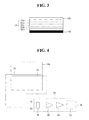
- FIGs. 4 to 6 schematically illustrate a configuration of the capacitive sensing unit TSC and a structure of a single-layered electrode unit of the touch screen panel TPNL.
- the capacitive sensing unit TSC is connected to electrode units TPL and TPR positioned inside the touch screen panel TPNL.
- the capacitive sensing unit TSC recognizes changes in a capacitance of the electrode units TPL and TPR when the user touches the touch screen panel TPNL to sense a touch position according to the user's touch operation.
- the capacitive sensing unit TSC may include a signal input unit SW, a signal amplifying unit AMP, a signal converting unit ADC, and a signal detecting unit LUT. Other configurations may be used.
- the signal input unit SW receives a signal through lines TS1 and TS2 connected to the electrode units TPL and TPR.
- the signal amplifying unit AMP amplifies the signal received from the signal input unit SW.
- the signal converting unit ADC converts an analog signal into a digital signal.
- the signal detecting unit LUT recognizes changes in the capacitance of the electrode units TPL and TPR using the digital signal to detect position data about the user's touch position. Then, the signal detecting unit LUT transmits the detected position data to a device CD to be used.
- the electrode units TPL and TPR are connected to the capacitive sensing unit TSC through lines TS1, TS2... TS10.
- the electrode units TPL and TPR may include first electrodes TPL, each of which is arranged from left to right of the touch screen panel TPNL and second electrodes TPR, each of which is arranged from right to left of the touch screen panel TPNL.
- the first electrodes TPL and the second electrodes TPR may be positioned on the same layer to be spaced apart from each other at a constant distance. Further, the first electrodes TPL and the second electrodes TPR may have different areas, so that the first electrodes TPL and the second electrodes TPR have different capacitances.
- the embodiment of the invention is not limited to the electrode units TPL and TPR shown in FIGs. 4 to 6 .
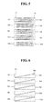
- FIGs. 7 to 9 schematically illustrate a configuration of the capacitive sensing unit TSC and a structure of a multi-layered electrode unit.
- the capacitive sensing unit TSC is connected to electrode units TPY and TPX positioned inside the touch screen panel TPNL.
- the capacitive sensing unit TSC recognizes changes in a capacitance of the electrode units TPY and TPX when the user touches the touch screen panel TPNL to sense a touch position according to the user's touch operation.
- the capacitive sensing unit TSC may include a signal input unit SW, a signal amplifying unit AMP, a signal converting unit ADC, and a signal detecting unit LUT. Other configurations may be used.
- the signal input unit SW receives a signal through lines TS1 and TS2 connected to the electrode units TPY and TPX.
- the signal amplifying unit AMP amplifies the signal received from the signal input unit SW.
- the signal converting unit ADC converts an analog signal into a digital signal.
- the signal detecting unit LUT recognizes changes in the capacitance of the electrode units TPY and TPX using the digital signal to detect position data about the user's touch position. Then, the signal detecting unit LUT transmits the detected position data to a device CD to be used.
- the electrode units TPY and TPX are connected to the capacitive sensing unit TSC through lines TS1, TS2... TS8.
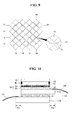
- the electrode units TPY and TPX may include first electrodes TPY arranged in a Y-axis direction of the touch screen panel TPNL and second electrodes TPX arranged in an X-axis direction of the touch screen panel TPNL.
- the first electrodes TPY and the second electrodes TPX may be positioned opposite each other with an insulating layer interposed between the first electrodes TPY and the second electrodes TPX. Namely, the first electrodes TPY and the second electrodes TPX may be positioned on different layer. As shown in FIG.
- a jumper electrode JP may be used to electrically connect electrodes on the same layer to one another.
- the jumper electrode JP helps to electrically connect the electrodes on the same layer to one another through a different layer.
- the embodiment of the invention is not limited to the electrode units TPY and TPX shown in FIGs. 7 to 9 .
- FIGs. 10 to 12 schematically illustrate a structure of an OLED display having a capacitive touch screen panel.
- an OLED display having a touch screen panel includes a panel 110, a shield electrode 140, a touch screen panel 150, a polarizing plate 160, an adhesive 170, a cover window 180, a first printed circuit board (PCB) 131, and a second PCB 135.
- PCB printed circuit board
- FIG. 10 illustrates the OLED display in which subpixels SP on the panel 110 emit light in a front direction and an electrode unit on the touch screen panel 150 has a single-layered structure.
- the panel 110 includes subpixels SP on one surface of a first substrate 110a and a second substrate 110b attached to the first substrate 110a.
- the shield electrode 140 is formed on one surface of the second substrate 110b, that does not face the subpixels SP, and is connected to a low potential voltage source.
- the low potential voltage source may be selected as a ground level voltage source supplying a ground level voltage to the panel 110.
- the touch screen panel 150 is formed on the shield electrode 140.
- the touch screen panel 150 includes an insulating layer 151 and an electrode unit 153.
- the insulating layer 151 provides insulation between the shield electrode 140 and the electrode unit 153.
- the electrode unit 153 as shown in FIGs. 5 and 6 , has a single-layered structure.
- the shield electrode 140 and the touch screen panel 150 are formed on the one surface of the second substrate 110b using a deposition method.
- the polarizing plate 160 is attached to the touch screen panel 150.
- the cover window 180 is attached to the polarizing plate 160 using the adhesive 170.
- the adhesive 170 may be formed in the form of a closed line surrounding an air layer AG, so that the air layer AG is formed between the polarizing plate 160 and the cover window 180, but is not limited thereto.
- the first PCB 131 is attached to a pad on the one surface of the first substrate 110a and receives a driving signal driving the subpixels SP from a driving device (for example, a timing controller).
- the second PCB 135 is attached to a pad on the one surface of the second substrate 110b and transmits a sensing signal generated by the touch screen panel 150 to a driving device (for example, a sensing unit).
- FIG. 11 illustrates the OLED display in which subpixels SP on the panel 110 emit light in a front direction and an electrode unit on the touch screen panel 150 has a multi-layered structure.
- the touch screen panel 150 includes a plurality of insulating layers 151 and 155 and a plurality of electrode units 153 and 157.
- the insulating layer 151 provides insulation between the shield electrode 140 and first electrodes of the electrode unit 153
- the insulating layer 155 provides insulation between the first electrodes of the electrode unit 153 and second electrodes of the electrode unit 157.
- the electrode units 153 and 157 as shown in FIGs. 8 and 9 , have a multi-layered structure. Since configuration of the panel 110, the shield electrode 140, the polarizing plate 160, and the cover window 180 may be substantially the same as those illustrated in FIG. 10 , a further description may be briefly made or may be entirely omitted.
- FIG. 12 illustrates the OLED display in which subpixels SP on the panel 110 emit light in a front direction and an electrode unit on the touch screen panel 150 has a multi-layered structure.
- the shield electrode 140 is formed inside the panel 110, i.e., on one surface of a second substrate 110b opposite the subpixels SP, and is connected to a low potential voltage source. Since configuration of the panel 110, the shield electrode 140, the touch screen panel 150, the polarizing plate 160, and the cover window 180 may be substantially the same as those illustrated in FIG. 11 , a further description may be briefly made or may be entirely omitted.
- first electrodes 153, a second insulating layer 155, and second electrodes 157 may be formed on the other surface of the second substrate 110b in the order named in a state where a first insulating layer 151 included in the touch screen panel 150 is omitted.
- the first substrate 110a includes a first pad area PA1 extending in an attaching direction of the first PCB 131 at one side of the first substrate 110a
- the second substrate 110b includes a second pad area PA2 extending in an attaching direction of the second PCB 135 at one side of the second substrate 110b.
- the OLED display illustrated in FIGs. 10 to 12 has a module structure in which the first PCB 131 can be led from the first pad area PA1 of the first substrate 110a and the second PCB 135 can be led from the second pad area PA2 of the second substrate 110b.
- FIGs. 13 and 14 schematically illustrate another structure of an OLED display having a capacitive touch screen panel.
- an OLED display having a touch screen panel includes a panel 210, a shield electrode 240, a touch screen panel 250, a polarizing plate 260, an adhesive 270, a cover window 280, a first PCB 231, and a second PCB 235.
- FIG. 13 illustrates the OLED display in which subpixels SP on the panel 210 emit light in a rear direction and an electrode unit on the touch screen panel 250 has a single-layered structure.
- the shield electrode 240 is formed on one surface of a first substrate 210a and is connected to a low potential voltage source.
- the low potential voltage source may be selected as a ground level voltage source supplying a ground level voltage to the panel 210.
- the touch screen panel 250 is formed on the shield electrode 240.
- the touch screen panel 250 includes an insulating layer 251 and an electrode unit 253.
- the insulating layer 251 provides insulation between the shield electrode 240 and the electrode unit 253.
- the electrode unit 253, as shown in FIGs. 5 and 6 has a single-layered structure.
- the shield electrode 240 and the touch screen panel 250 are formed on the one surface of the first substrate 210a using a deposition method.
- the polarizing plate 260 is attached to the touch screen panel 250.
- the cover window 280 is attached to the polarizing plate 260 using the adhesive 270.
- the adhesive 270 may be formed in the form of a closed line surrounding an air layer AG, so that the air layer AG is formed between the polarizing plate 260 and the cover window 280, but is not limited thereto.
- the first PCB 231 is attached to a pad on the other surface of the first substrate 210a and receives a driving signal driving the subpixels SP from a driving device (for example, a timing controller).
- the second PCB 235 is attached to a pad on the one surface of the first substrate 210a and transmits a sensing signal generated by the touch screen panel 250 to a driving device (for example, a sensing unit).
- FIG. 14 illustrates the OLED display in which subpixels SP on the panel 210 emit light in a rear direction and an electrode unit on the touch screen panel 250 has a multi-layered structure.
- the touch screen panel 250 includes a plurality of insulating layers 251 and 255 and a plurality of electrode units 253 and 257.
- the insulating layer 251 provides insulation between the shield electrode 240 and first electrodes of the electrode unit 253, and the insulating layer 255 provides insulation between the first electrodes of the electrode unit 253 and second electrodes of the electrode unit 257.
- the electrode units 253 and 257 as shown in FIGs. 8 and 9 , have a multi-layered structure. Since configuration of the panel 210, the shield electrode 240, the polarizing plate 260, and the cover window 280 may be substantially the same as those illustrated in FIG. 13 , a further description may be briefly made or may be entirely omitted.
- the first substrate 210a includes a first pad area PA1 extending in an attaching direction of the first PCB 231 and the second PCB 235 at one side of the first substrate 210a. Because the first substrate 210a includes the first pad area PA1, a length of the first substrate 210a is longer than a length of the second substrate 210 by a length of the first pad area PA1.
- the OLED display illustrated in FIGs. 13 and 14 has a module structure in which the first PCB 231 and the second PCB 235 respectively formed on both surfaces of the first substrate 210a can be led from the first pad area PA1.
- FIGs. 15 and 16 schematically illustrate another structure of an OLED display having a capacitive touch screen panel.
- an OLED display having a touch screen panel includes a panel 310, a shield electrode 340, a touch screen panel 350, a polarizing plate 360, an adhesive 370, a cover window 380, a first PCB 331, and a second PCB 335.
- FIG. 15 illustrates the OLED display in which subpixels SP on the panel 310 emit light in a rear direction and an electrode unit on the touch screen panel 350 has a single-layered structure.
- the shield electrode 340 is formed on one surface of a first substrate 310a and is connected to a low potential voltage source.
- the low potential voltage source may be selected as a ground level voltage source supplying a ground level voltage to the panel 310.
- the touch screen panel 350 is formed on the shield electrode 340.
- the touch screen panel 350 includes an insulating layer 351 and an electrode unit 353.
- the insulating layer 351 provides insulation between the shield electrode 340 and the electrode unit 353.
- the electrode unit 353, as shown in FIGs. 5 and 6 has a single-layered structure.
- the shield electrode 340 and the touch screen panel 350 are formed on the one surface of the first substrate 310a using a deposition method.
- the polarizing plate 360 is attached to the touch screen panel 350.
- the cover window 380 is attached to the polarizing plate 360 using the adhesive 370.
- the adhesive 370 may be formed in the form of a closed line surrounding an air layer AG, so that the air layer AG is formed between the polarizing plate 360 and the cover window 380, but is not limited thereto.
- the first PCB 331 is attached to a pad on the other surface of the first substrate 310a and receives a driving signal driving the subpixels SP from a driving device (for example, a timing controller).
- the second PCB 335 is attached to a pad on the one surface of the first substrate 310a and transmits a sensing signal generated by the touch screen panel 350 to a driving device (for example, a sensing unit).
- FIG. 16 illustrates the OLED display in which subpixels SP on the panel 310 emit light in a rear direction and an electrode unit on the touch screen panel 350 has a multi-layered structure.
- the touch screen panel 350 includes a plurality of insulating layers 351 and 355 and a plurality of electrode units 353 and 357.
- the insulating layer 351 provides insulation between the shield electrode 340 and first electrodes of the electrode unit 353, and the insulating layer 355 provides insulation between the first electrodes of the electrode unit 353 and second electrodes of the electrode unit 357.
- the electrode units 353 and 357 as shown in FIGs. 8 and 9 , have a multi-layered structure. Since configuration of the panel 310, the shield electrode 340, the polarizing plate 360, and the cover window 380 may be substantially the same as those illustrated in FIG. 15 , a further description may be briefly made or may be entirely omitted.
- the first substrate 310a includes a first pad area PA1 extending in an attaching direction of the first PCB 331 at one side of the first substrate 310a and a second pad area PA11 extending in an attaching direction of the second PCB 335 at the other side of the first substrate 310a. Because the first substrate 210a includes the first pad area PA1 and the second pad area PA11, a length of the first substrate 310a is longer than a length of the second substrate 310b by a sum of lengths of the first and second pad areas PA1 and PA11.
- the OLED display illustrated in FIGs. 15 and 16 has a module structure in which the first PCB 331 and the second PCB 335 can be respectively led from the first pad area PA1 and the second pad area PA11 at both sides of the first substrate 310a.
- the OLED display having the touch screen panel because the shield electrode connected to the low potential voltage source is formed on the panel and the touch screen panel is formed on the shield electrode, the OLED display having the touch screen panel with a strong resistance against external and internal noises can be provided. Further, the OLED display having the touch screen panel can be used in various applications.
- an organic light emitting diode (OLED) display comprising: a plurality of subpixels on one surface of a first substrate; a second substrate attached to the first substrate; a shield electrode on one surface of the second substrate that is not opposite to the subpixels, the shield electrode being connected to a low potential voltage source; a touch screen panel on the shield electrode; a first printed circuit board (PCB) attached to the one surface of the first substrate, the first PCB receiving a driving signal driving the subpixels from a driving device; and a second PCB attached to the one surface of the second substrate, the second PCB transmitting a sensing signal generated by the touch screen panel to an external device.
- PCB printed circuit board
- the first substrate includes a first pad area extending in an attaching direction of the first PCB at one side of the first substrate
- the second substrate includes a second pad area extending in an attaching direction of the second PCB at one side of the second substrate.
- the touch screen panel has a single-layered structure including one transparent electrode or a multi-layered structure including two transparent electrodes.
- the OLED display further comprises: a polarizing plate on the touch screen panel; and a cover window on the polarizing plate, wherein the polarizing plate and the cover window are attached to each other using an adhesive surrounding an air layer, so that the air layer is formed between the polarizing plate and the cover window.
- an organic light emitting diode (OLED) display comprises: a plurality of subpixels on one surface of a first substrate; a second substrate attached to the first substrate; a shield electrode on other surface of the first substrate on which the subpixels are not formed, the shield electrode being connected to a low potential voltage source; a touch screen panel on the shield electrode; a first printed circuit board (PCB) attached to the one surface of the first substrate, the first PCB receiving a driving signal driving the subpixels from a driving device; and a second PCB attached to the other surface of the first substrate, the second PCB transmitting a sensing signal generated by the touch screen panel to an external device.
- PCB printed circuit board
- the first substrate includes a first pad area extending in an attaching direction of the first and second PCBs.
- a length of the first substrate is longer than a length of the second substrate by a length of the first pad area.
- the touch screen panel has a single-layered structure including one transparent electrode or a multi-layered structure including two transparent electrodes.
- the OLED display further comprises: a polarizing plate on the touch screen panel; and a cover window on the polarizing plate, wherein the polarizing plate and the cover window are attached to each other using an adhesive surrounding an air layer, so that the air layer is formed between the polarizing plate and the cover window.
- an organic light emitting diode (OLED) display comprises: a plurality of subpixels on one surface of a first substrate; a second substrate attached to the first substrate; a shield electrode on one surface of the second substrate opposite the subpixels, the shield electrode being connected to a low potential voltage source; a touch screen panel on other surface of the second substrate that is not opposite to the subpixels; a first printed circuit board (PCB) attached to the one surface of the first substrate, the first PCB receiving a driving signal driving the subpixels from a driving device; and a second PCB attached to other surface of the first substrate, the second PCB transmitting a sensing signal generated by the touch screen panel to an external device.
- PCB printed circuit board
- the first substrate includes a first pad area extending in an attaching direction of the first PCB at one side of the first substrate and a second pad area extending in an attaching direction of the second PCB at other side of the first substrate.
- a length of the first substrate is longer than a length of the second substrate by a sum of lengths of the first and second pad areas.
- the touch screen panel has a single-layered structure including one transparent electrode or a multi-layered structure including two transparent electrodes.
- the OLED display further comprises: a polarizing plate on the touch screen panel; and a cover window on the polarizing plate, wherein the polarizing plate and the cover window are attached to each other using an adhesive surrounding an air layer, so that the air layer is formed between the polarizing plate and the cover window.
Landscapes
- Engineering & Computer Science (AREA)
- General Engineering & Computer Science (AREA)
- Theoretical Computer Science (AREA)
- Human Computer Interaction (AREA)
- Physics & Mathematics (AREA)
- General Physics & Mathematics (AREA)
- Microelectronics & Electronic Packaging (AREA)
- Computer Networks & Wireless Communication (AREA)
- Electroluminescent Light Sources (AREA)
- Devices For Indicating Variable Information By Combining Individual Elements (AREA)
- Position Input By Displaying (AREA)
Applications Claiming Priority (2)
| Application Number | Priority Date | Filing Date | Title |
|---|---|---|---|
| KR1020090050572A KR101323434B1 (ko) | 2009-06-08 | 2009-06-08 | 유기전계발광표시장치 |
| EP09170313A EP2261986A3 (de) | 2009-06-08 | 2009-09-15 | Berührungsbildschirm mit organischen lichtemittierenden Dioden |
Related Parent Applications (1)
| Application Number | Title | Priority Date | Filing Date |
|---|---|---|---|
| EP09170313A Division EP2261986A3 (de) | 2009-06-08 | 2009-09-15 | Berührungsbildschirm mit organischen lichtemittierenden Dioden |
Publications (3)
| Publication Number | Publication Date |
|---|---|
| EP2869346A2 true EP2869346A2 (de) | 2015-05-06 |
| EP2869346A3 EP2869346A3 (de) | 2015-11-04 |
| EP2869346B1 EP2869346B1 (de) | 2022-05-25 |
Family
ID=41647041
Family Applications (2)
| Application Number | Title | Priority Date | Filing Date |
|---|---|---|---|
| EP09170313A Withdrawn EP2261986A3 (de) | 2009-06-08 | 2009-09-15 | Berührungsbildschirm mit organischen lichtemittierenden Dioden |
| EP15152613.4A Active EP2869346B1 (de) | 2009-06-08 | 2009-09-15 | Organische lichtemittierende Diodenanzeige |
Family Applications Before (1)
| Application Number | Title | Priority Date | Filing Date |
|---|---|---|---|
| EP09170313A Withdrawn EP2261986A3 (de) | 2009-06-08 | 2009-09-15 | Berührungsbildschirm mit organischen lichtemittierenden Dioden |
Country Status (5)
| Country | Link |
|---|---|
| US (1) | US8599149B2 (de) |
| EP (2) | EP2261986A3 (de) |
| JP (1) | JP5290128B2 (de) |
| KR (1) | KR101323434B1 (de) |
| CN (1) | CN101908314B (de) |
Families Citing this family (55)
| Publication number | Priority date | Publication date | Assignee | Title |
|---|---|---|---|---|
| US9148497B2 (en) * | 2009-04-22 | 2015-09-29 | Nokia Technologies Oy | Display with improved electromagnetic compatibility characteristics |
| KR101322981B1 (ko) * | 2009-12-01 | 2013-10-29 | 엘지디스플레이 주식회사 | 터치 소자를 구비한 표시장치 |
| TWI615743B (zh) * | 2010-03-25 | 2018-02-21 | 永恆科技有限公司 | 觸控面板及其製造方法 |
| KR20110110593A (ko) | 2010-04-01 | 2011-10-07 | 삼성모바일디스플레이주식회사 | 평판 표시 장치 |
| KR101886801B1 (ko) * | 2010-09-14 | 2018-08-10 | 삼성디스플레이 주식회사 | 터치 스크린 패널 일체형 평판표시장치 |
| KR20120029008A (ko) * | 2010-09-15 | 2012-03-26 | 삼성전자주식회사 | 온-셀 tsp 능동형유기발광다이오드 표시장치 |
| US8417376B1 (en) * | 2011-01-28 | 2013-04-09 | Christopher M. Smolen | Method and means for viewing selecting and taking action relative to an item of a group of items |
| JP5778961B2 (ja) * | 2011-03-29 | 2015-09-16 | 株式会社Joled | 表示装置および電子機器 |
| KR20120130990A (ko) * | 2011-05-24 | 2012-12-04 | 삼성전자주식회사 | 디지타이저 통합형 디스플레이 |
| KR101381817B1 (ko) | 2011-06-30 | 2014-04-07 | 삼성디스플레이 주식회사 | 터치 스크린 패널 |
| US9469528B2 (en) * | 2011-08-11 | 2016-10-18 | Cheil Industries, Inc. | Adhesive composition, adhesive film including the same, method of preparing adhesive film, and display member using the same |
| TW201312526A (zh) * | 2011-09-02 | 2013-03-16 | Wintek Corp | 觸控顯示面板 |
| JP5667960B2 (ja) * | 2011-10-14 | 2015-02-12 | 株式会社ジャパンディスプレイ | 表示装置、タッチ検出装置、および電子機器 |
| WO2013076994A1 (ja) * | 2011-11-24 | 2013-05-30 | パナソニック株式会社 | 頭部装着型ディスプレイ装置 |
| KR101908501B1 (ko) * | 2011-12-07 | 2018-10-17 | 엘지디스플레이 주식회사 | 터치 스크린 일체형 유기 발광 표시 장치 및 이의 제조 방법 |
| TWI462069B (zh) * | 2011-12-30 | 2014-11-21 | Au Optronics Corp | 觸控顯示面板 |
| US10621809B2 (en) | 2012-01-19 | 2020-04-14 | Christopher M. Smolen | Digital currency enabled vending machine |
| EP2836960B1 (de) * | 2012-04-10 | 2018-09-26 | Idex Asa | Biometrische erfassung |
| TWI523180B (zh) * | 2012-05-07 | 2016-02-21 | 友達光電股份有限公司 | 觸控面板、觸控顯示面板以及觸控顯示裝置 |
| KR101469485B1 (ko) * | 2012-08-13 | 2014-12-05 | 엘지디스플레이 주식회사 | 유기 발광 표시 장치 및 이의 제조 방법 |
| KR101341030B1 (ko) | 2012-08-29 | 2013-12-13 | 엘지디스플레이 주식회사 | 유기 발광 표시 장치 및 이의 제조 방법 |
| KR101469487B1 (ko) | 2012-09-18 | 2014-12-05 | 엘지디스플레이 주식회사 | 유기 발광 표시 장치 |
| KR102056929B1 (ko) * | 2013-03-08 | 2019-12-18 | 삼성디스플레이 주식회사 | 터치스크린패널 일체형 표시장치 |
| KR102111625B1 (ko) * | 2013-06-28 | 2020-05-18 | 삼성디스플레이 주식회사 | 터치센서 내장형 표시장치 및 그의 제조방법 |
| CN104635967B (zh) * | 2013-11-12 | 2018-04-10 | 宸鸿光电科技股份有限公司 | 有机发光二极管触控显示设备 |
| CN109062448B (zh) * | 2013-11-12 | 2021-07-02 | 宸鸿光电科技股份有限公司 | 有机发光二极管触控显示设备 |
| CN104637974B (zh) * | 2013-11-12 | 2018-10-26 | 宸鸿光电科技股份有限公司 | 有机发光二极管触控显示设备 |
| KR102189313B1 (ko) * | 2013-11-28 | 2020-12-10 | 삼성디스플레이 주식회사 | 표시 장치 |
| CN103943061B (zh) * | 2013-12-11 | 2016-08-17 | 上海天马微电子有限公司 | 一种内置触控结构的oled显示装置 |
| KR102208417B1 (ko) * | 2013-12-23 | 2021-01-28 | 삼성디스플레이 주식회사 | 표시 장치 및 표시 장치의 제조 방법 |
| US9588622B2 (en) * | 2013-12-31 | 2017-03-07 | Shenzhen China Star Optoelectronics Technology Co., Ltd | Single layer capacitive touch module backlight module |
| JP6277376B2 (ja) | 2014-01-29 | 2018-02-14 | 株式会社Joled | 画像表示装置 |
| TWI764064B (zh) * | 2014-03-13 | 2022-05-11 | 日商半導體能源研究所股份有限公司 | 撓性裝置 |
| CN103985350B (zh) | 2014-04-29 | 2016-09-07 | 上海天马有机发光显示技术有限公司 | 一种像素电路、显示面板、显示装置和驱动方法 |
| KR102353034B1 (ko) * | 2014-08-11 | 2022-01-19 | 삼성디스플레이 주식회사 | 플렉서블 유기 발광 표시 장치 |
| KR102296733B1 (ko) * | 2014-11-06 | 2021-09-01 | 삼성디스플레이 주식회사 | 유기 발광 표시 장치 |
| KR102253530B1 (ko) | 2014-11-21 | 2021-05-18 | 삼성디스플레이 주식회사 | 터치 스크린 패널을 구비한 표시 장치 |
| KR102350084B1 (ko) * | 2015-01-15 | 2022-01-11 | 삼성디스플레이 주식회사 | 터치 패널 및 이를 이용한 표시장치 |
| KR102315671B1 (ko) | 2015-01-19 | 2021-10-21 | 삼성디스플레이 주식회사 | 표시 장치 |
| CN104820519B (zh) * | 2015-05-08 | 2018-03-30 | 厦门天马微电子有限公司 | 触控显示面板及触摸显示装置 |
| KR102416017B1 (ko) * | 2015-06-15 | 2022-07-04 | 삼성디스플레이 주식회사 | 표시 장치 |
| KR102342596B1 (ko) | 2015-06-26 | 2021-12-24 | 삼성디스플레이 주식회사 | 표시 장치 |
| US10325131B2 (en) * | 2015-06-30 | 2019-06-18 | Synaptics Incorporated | Active matrix capacitive fingerprint sensor for display integration based on charge sensing by a 2-TFT pixel architecture |
| KR101747263B1 (ko) * | 2015-09-25 | 2017-06-14 | 엘지디스플레이 주식회사 | 드라이버ic 및 이를 이용한 표시장치 |
| KR102548931B1 (ko) * | 2016-03-22 | 2023-06-30 | 삼성디스플레이 주식회사 | 표시 장치 |
| CN105679232A (zh) * | 2016-03-28 | 2016-06-15 | 王金 | 触控式立体有机电致发光显示装置 |
| KR102564349B1 (ko) * | 2016-09-30 | 2023-08-04 | 엘지디스플레이 주식회사 | 유기 발광 표시 장치 |
| JP6734771B2 (ja) * | 2016-12-28 | 2020-08-05 | 株式会社ジャパンディスプレイ | 表示装置 |
| KR102478497B1 (ko) * | 2017-09-22 | 2022-12-16 | 삼성디스플레이 주식회사 | 표시 장치 및 헤드 마운트 표시 장치 |
| KR102424172B1 (ko) * | 2018-04-25 | 2022-07-25 | 삼성디스플레이 주식회사 | 전자 장치 |
| CN109164935B (zh) * | 2018-08-24 | 2022-07-19 | 敦泰电子有限公司 | 触控显示面板、触控驱动电路和触控驱动方法 |
| KR102640257B1 (ko) * | 2018-11-08 | 2024-02-26 | 엘지디스플레이 주식회사 | 표시패널 |
| KR102589890B1 (ko) * | 2018-12-31 | 2023-10-13 | 엘지디스플레이 주식회사 | 터치 일체형 전계 발광 조명장치 |
| KR102934006B1 (ko) * | 2020-12-29 | 2026-03-04 | 엘지디스플레이 주식회사 | 백색 발광 소자 및 이를 포함한 발광 표시 장치 |
| CN115904133B (zh) | 2021-08-16 | 2025-09-26 | 京东方科技集团股份有限公司 | 触控显示基板及制备方法、触控显示装置 |
Family Cites Families (31)
| Publication number | Priority date | Publication date | Assignee | Title |
|---|---|---|---|---|
| JPH05224813A (ja) | 1992-02-17 | 1993-09-03 | Sharp Corp | 手書き入力装置 |
| JPH09203890A (ja) | 1996-01-25 | 1997-08-05 | Sharp Corp | 入力機能付き液晶表示素子および反射型入力機能付き液晶表示素子、並びにそれらの製造方法 |
| JPH11167097A (ja) | 1997-12-03 | 1999-06-22 | Seiko Epson Corp | 入力機能付液晶表示装置、その製造方法、および入力機能付液晶表示装置を用いた電子機器 |
| JP3986225B2 (ja) * | 1999-11-26 | 2007-10-03 | カシオ計算機株式会社 | 積層型表示装置 |
| US6395863B2 (en) * | 2000-02-02 | 2002-05-28 | Microtouch Systems, Inc. | Touch screen with polarizer and method of making same |
| JP2002148592A (ja) * | 2000-08-31 | 2002-05-22 | Sumitomo Chem Co Ltd | 液晶表示装置 |
| JP2003215344A (ja) * | 2001-03-29 | 2003-07-30 | Seiko Epson Corp | 偏光子、およびこの偏光子を用いた光学機器 |
| US6814642B2 (en) * | 2001-04-04 | 2004-11-09 | Eastman Kodak Company | Touch screen display and method of manufacture |
| US6424094B1 (en) * | 2001-05-15 | 2002-07-23 | Eastman Kodak Company | Organic electroluminescent display with integrated resistive touch screen |
| US7106307B2 (en) * | 2001-05-24 | 2006-09-12 | Eastman Kodak Company | Touch screen for use with an OLED display |
| KR20020090054A (ko) * | 2001-05-26 | 2002-11-30 | 삼성에스디아이 주식회사 | 플라즈마 표시장치 |
| JP2003099193A (ja) * | 2001-09-21 | 2003-04-04 | Tohoku Pioneer Corp | 画面表示入力装置 |
| WO2003075207A2 (en) * | 2002-03-01 | 2003-09-12 | Planar Systems, Inc. | Reflection resistant touch screens |
| TW586096B (en) * | 2003-04-25 | 2004-05-01 | Ind Tech Res Inst | Dual-screen organic electroluminescent display |
| KR100591798B1 (ko) * | 2003-06-27 | 2006-06-20 | 엘지.필립스 엘시디 주식회사 | 능동 구동형 유기 전계발광 소자 패널 |
| JP2005038231A (ja) | 2003-07-16 | 2005-02-10 | Kawaguchiko Seimitsu Co Ltd | 画面入力型表示装置 |
| JP4174798B2 (ja) | 2003-07-25 | 2008-11-05 | シャープ株式会社 | 表示装置 |
| JP2005158008A (ja) * | 2003-11-06 | 2005-06-16 | Matsushita Electric Ind Co Ltd | タッチパネルおよびこれを用いたタッチパネル付き液晶表示装置 |
| US6885157B1 (en) * | 2003-11-25 | 2005-04-26 | Eastman Kodak Company | Integrated touch screen and OLED flat-panel display |
| JP2006195316A (ja) * | 2005-01-17 | 2006-07-27 | Seiko Epson Corp | 電気光学装置および電子機器 |
| TWI270025B (en) * | 2005-03-21 | 2007-01-01 | Au Optronics Corp | Dual emission display with integrated touch screen and fabricating method thereof |
| US7864160B2 (en) * | 2005-10-05 | 2011-01-04 | 3M Innovative Properties Company | Interleaved electrodes for touch sensing |
| WO2007066590A1 (ja) | 2005-12-05 | 2007-06-14 | Seiko Instruments Inc. | 表示機器および表示機器の製造方法 |
| JP4624462B2 (ja) * | 2006-03-08 | 2011-02-02 | シャープ株式会社 | 表示装置 |
| TWI317086B (en) * | 2006-04-14 | 2009-11-11 | Ritdisplay Corp | Top-emitting organic led display having transparent touch panel |
| KR101374887B1 (ko) * | 2006-05-16 | 2014-03-13 | 삼성디스플레이 주식회사 | 표시 패널 |
| JP5051690B2 (ja) * | 2007-01-30 | 2012-10-17 | 株式会社ジャパンディスプレイウェスト | 入力機能付表示装置 |
| JP4910780B2 (ja) * | 2007-03-02 | 2012-04-04 | セイコーエプソン株式会社 | 入力機能付有機エレクトロルミネッセンス装置、及び電子機器 |
| KR20080089910A (ko) * | 2007-04-03 | 2008-10-08 | 엘지디스플레이 주식회사 | 터치 패널 일체형 액정표시장치 |
| KR100873080B1 (ko) * | 2007-05-10 | 2008-12-09 | 삼성모바일디스플레이주식회사 | 유기 전계 발광표시장치 |
| TW200921483A (en) * | 2007-11-09 | 2009-05-16 | Tpk Touch Solutions Inc | Touch-control display panel with an electric-field shielding layer |
-
2009
- 2009-06-08 KR KR1020090050572A patent/KR101323434B1/ko active Active
- 2009-09-15 EP EP09170313A patent/EP2261986A3/de not_active Withdrawn
- 2009-09-15 EP EP15152613.4A patent/EP2869346B1/de active Active
- 2009-10-21 CN CN2009102058805A patent/CN101908314B/zh active Active
- 2009-10-27 US US12/588,771 patent/US8599149B2/en active Active
- 2009-11-10 JP JP2009256817A patent/JP5290128B2/ja active Active
Non-Patent Citations (1)
| Title |
|---|
| None |
Also Published As
| Publication number | Publication date |
|---|---|
| EP2261986A3 (de) | 2012-08-01 |
| CN101908314A (zh) | 2010-12-08 |
| EP2869346A3 (de) | 2015-11-04 |
| JP2010282171A (ja) | 2010-12-16 |
| JP5290128B2 (ja) | 2013-09-18 |
| KR20100131797A (ko) | 2010-12-16 |
| US20100309150A1 (en) | 2010-12-09 |
| EP2869346B1 (de) | 2022-05-25 |
| KR101323434B1 (ko) | 2013-10-29 |
| EP2261986A2 (de) | 2010-12-15 |
| US8599149B2 (en) | 2013-12-03 |
| CN101908314B (zh) | 2013-03-20 |
Similar Documents
| Publication | Publication Date | Title |
|---|---|---|
| US8599149B2 (en) | Organic light emitting diode display | |
| US8373340B2 (en) | Organic electroluminescent display device | |
| KR101258258B1 (ko) | 유기전계발광표시장치 | |
| CN101877201B (zh) | 显示装置 | |
| KR20110037337A (ko) | 유기전계발광표시장치와 이의 제조방법 | |
| US8330675B2 (en) | Organic light emitting display | |
| KR101596968B1 (ko) | 유기전계발광표시장치와 이의 제조방법 | |
| JP2025172801A (ja) | 発光表示装置 | |
| KR101633104B1 (ko) | 유기전계발광표시장치 | |
| KR101577827B1 (ko) | 유기전계발광표시장치 | |
| KR101589750B1 (ko) | 유기전계발광표시장치 | |
| KR101667043B1 (ko) | 유기전계발광표시장치 | |
| KR20100111991A (ko) | 유기전계발광표시장치 | |
| KR20180069326A (ko) | 터치 스크린을 구비한 표시 장치 |
Legal Events
| Date | Code | Title | Description |
|---|---|---|---|
| PUAI | Public reference made under article 153(3) epc to a published international application that has entered the european phase |
Free format text: ORIGINAL CODE: 0009012 |
|
| 17P | Request for examination filed |
Effective date: 20150127 |
|
| AC | Divisional application: reference to earlier application |
Ref document number: 2261986 Country of ref document: EP Kind code of ref document: P |
|
| AK | Designated contracting states |
Kind code of ref document: A2 Designated state(s): AT BE BG CH CY CZ DE DK EE ES FI FR GB GR HR HU IE IS IT LI LT LU LV MC MK MT NL NO PL PT RO SE SI SK SM TR |
|
| PUAL | Search report despatched |
Free format text: ORIGINAL CODE: 0009013 |
|
| RIN1 | Information on inventor provided before grant (corrected) |
Inventor name: SEO, SANGWOO Inventor name: CHOI, HOWON Inventor name: LEE, JAEDO |
|
| AK | Designated contracting states |
Kind code of ref document: A3 Designated state(s): AT BE BG CH CY CZ DE DK EE ES FI FR GB GR HR HU IE IS IT LI LT LU LV MC MK MT NL NO PL PT RO SE SI SK SM TR |
|
| RIC1 | Information provided on ipc code assigned before grant |
Ipc: H01L 27/32 20060101AFI20150930BHEP Ipc: G06F 3/041 20060101ALI20150930BHEP Ipc: G06F 3/044 20060101ALI20150930BHEP |
|
| RIN1 | Information on inventor provided before grant (corrected) |
Inventor name: LEE, JAEDO Inventor name: CHOI, HOWON Inventor name: SEO, SANGWOO |
|
| RBV | Designated contracting states (corrected) |
Designated state(s): AT BE BG CH CY CZ DE DK EE ES FI FR GB GR HR HU IE IS IT LI LT LU LV MC MK MT NL NO PL PT RO SE SI SK SM TR |
|
| RIN1 | Information on inventor provided before grant (corrected) |
Inventor name: CHOI, HOWON Inventor name: LEE, JAEDO Inventor name: SEO, SANGWOO |
|
| STAA | Information on the status of an ep patent application or granted ep patent |
Free format text: STATUS: EXAMINATION IS IN PROGRESS |
|
| 17Q | First examination report despatched |
Effective date: 20180420 |
|
| RIC1 | Information provided on ipc code assigned before grant |
Ipc: G06F 3/041 20060101ALI20211208BHEP Ipc: G06F 3/044 20060101ALI20211208BHEP Ipc: H01L 27/32 20060101AFI20211208BHEP |
|
| GRAP | Despatch of communication of intention to grant a patent |
Free format text: ORIGINAL CODE: EPIDOSNIGR1 |
|
| STAA | Information on the status of an ep patent application or granted ep patent |
Free format text: STATUS: GRANT OF PATENT IS INTENDED |
|
| INTG | Intention to grant announced |
Effective date: 20220125 |
|
| GRAS | Grant fee paid |
Free format text: ORIGINAL CODE: EPIDOSNIGR3 |
|
| GRAA | (expected) grant |
Free format text: ORIGINAL CODE: 0009210 |
|
| STAA | Information on the status of an ep patent application or granted ep patent |
Free format text: STATUS: THE PATENT HAS BEEN GRANTED |
|
| AC | Divisional application: reference to earlier application |
Ref document number: 2261986 Country of ref document: EP Kind code of ref document: P |
|
| AK | Designated contracting states |
Kind code of ref document: B1 Designated state(s): AT BE BG CH CY CZ DE DK EE ES FI FR GB GR HR HU IE IS IT LI LT LU LV MC MK MT NL NO PL PT RO SE SI SK SM TR |
|
| REG | Reference to a national code |
Ref country code: GB Ref legal event code: FG4D |
|
| REG | Reference to a national code |
Ref country code: CH Ref legal event code: EP |
|
| REG | Reference to a national code |
Ref country code: DE Ref legal event code: R096 Ref document number: 602009064454 Country of ref document: DE |
|
| REG | Reference to a national code |
Ref country code: AT Ref legal event code: REF Ref document number: 1494601 Country of ref document: AT Kind code of ref document: T Effective date: 20220615 |
|
| REG | Reference to a national code |
Ref country code: IE Ref legal event code: FG4D |
|
| REG | Reference to a national code |
Ref country code: LT Ref legal event code: MG9D |
|
| REG | Reference to a national code |
Ref country code: NL Ref legal event code: MP Effective date: 20220525 |
|
| REG | Reference to a national code |
Ref country code: AT Ref legal event code: MK05 Ref document number: 1494601 Country of ref document: AT Kind code of ref document: T Effective date: 20220525 |
|
| PG25 | Lapsed in a contracting state [announced via postgrant information from national office to epo] |
Ref country code: SE Free format text: LAPSE BECAUSE OF FAILURE TO SUBMIT A TRANSLATION OF THE DESCRIPTION OR TO PAY THE FEE WITHIN THE PRESCRIBED TIME-LIMIT Effective date: 20220525 Ref country code: PT Free format text: LAPSE BECAUSE OF FAILURE TO SUBMIT A TRANSLATION OF THE DESCRIPTION OR TO PAY THE FEE WITHIN THE PRESCRIBED TIME-LIMIT Effective date: 20220926 Ref country code: NO Free format text: LAPSE BECAUSE OF FAILURE TO SUBMIT A TRANSLATION OF THE DESCRIPTION OR TO PAY THE FEE WITHIN THE PRESCRIBED TIME-LIMIT Effective date: 20220825 Ref country code: NL Free format text: LAPSE BECAUSE OF FAILURE TO SUBMIT A TRANSLATION OF THE DESCRIPTION OR TO PAY THE FEE WITHIN THE PRESCRIBED TIME-LIMIT Effective date: 20220525 Ref country code: LT Free format text: LAPSE BECAUSE OF FAILURE TO SUBMIT A TRANSLATION OF THE DESCRIPTION OR TO PAY THE FEE WITHIN THE PRESCRIBED TIME-LIMIT Effective date: 20220525 Ref country code: HR Free format text: LAPSE BECAUSE OF FAILURE TO SUBMIT A TRANSLATION OF THE DESCRIPTION OR TO PAY THE FEE WITHIN THE PRESCRIBED TIME-LIMIT Effective date: 20220525 Ref country code: GR Free format text: LAPSE BECAUSE OF FAILURE TO SUBMIT A TRANSLATION OF THE DESCRIPTION OR TO PAY THE FEE WITHIN THE PRESCRIBED TIME-LIMIT Effective date: 20220826 Ref country code: FI Free format text: LAPSE BECAUSE OF FAILURE TO SUBMIT A TRANSLATION OF THE DESCRIPTION OR TO PAY THE FEE WITHIN THE PRESCRIBED TIME-LIMIT Effective date: 20220525 Ref country code: ES Free format text: LAPSE BECAUSE OF FAILURE TO SUBMIT A TRANSLATION OF THE DESCRIPTION OR TO PAY THE FEE WITHIN THE PRESCRIBED TIME-LIMIT Effective date: 20220525 Ref country code: BG Free format text: LAPSE BECAUSE OF FAILURE TO SUBMIT A TRANSLATION OF THE DESCRIPTION OR TO PAY THE FEE WITHIN THE PRESCRIBED TIME-LIMIT Effective date: 20220825 Ref country code: AT Free format text: LAPSE BECAUSE OF FAILURE TO SUBMIT A TRANSLATION OF THE DESCRIPTION OR TO PAY THE FEE WITHIN THE PRESCRIBED TIME-LIMIT Effective date: 20220525 |
|
| REG | Reference to a national code |
Ref country code: DE Ref legal event code: R079 Ref document number: 602009064454 Country of ref document: DE Free format text: PREVIOUS MAIN CLASS: H01L0027320000 Ipc: H10K0059000000 |
|
| PG25 | Lapsed in a contracting state [announced via postgrant information from national office to epo] |
Ref country code: PL Free format text: LAPSE BECAUSE OF FAILURE TO SUBMIT A TRANSLATION OF THE DESCRIPTION OR TO PAY THE FEE WITHIN THE PRESCRIBED TIME-LIMIT Effective date: 20220525 Ref country code: LV Free format text: LAPSE BECAUSE OF FAILURE TO SUBMIT A TRANSLATION OF THE DESCRIPTION OR TO PAY THE FEE WITHIN THE PRESCRIBED TIME-LIMIT Effective date: 20220525 Ref country code: IS Free format text: LAPSE BECAUSE OF FAILURE TO SUBMIT A TRANSLATION OF THE DESCRIPTION OR TO PAY THE FEE WITHIN THE PRESCRIBED TIME-LIMIT Effective date: 20220925 |
|
| PG25 | Lapsed in a contracting state [announced via postgrant information from national office to epo] |
Ref country code: SM Free format text: LAPSE BECAUSE OF FAILURE TO SUBMIT A TRANSLATION OF THE DESCRIPTION OR TO PAY THE FEE WITHIN THE PRESCRIBED TIME-LIMIT Effective date: 20220525 Ref country code: SK Free format text: LAPSE BECAUSE OF FAILURE TO SUBMIT A TRANSLATION OF THE DESCRIPTION OR TO PAY THE FEE WITHIN THE PRESCRIBED TIME-LIMIT Effective date: 20220525 Ref country code: RO Free format text: LAPSE BECAUSE OF FAILURE TO SUBMIT A TRANSLATION OF THE DESCRIPTION OR TO PAY THE FEE WITHIN THE PRESCRIBED TIME-LIMIT Effective date: 20220525 Ref country code: EE Free format text: LAPSE BECAUSE OF FAILURE TO SUBMIT A TRANSLATION OF THE DESCRIPTION OR TO PAY THE FEE WITHIN THE PRESCRIBED TIME-LIMIT Effective date: 20220525 Ref country code: DK Free format text: LAPSE BECAUSE OF FAILURE TO SUBMIT A TRANSLATION OF THE DESCRIPTION OR TO PAY THE FEE WITHIN THE PRESCRIBED TIME-LIMIT Effective date: 20220525 Ref country code: CZ Free format text: LAPSE BECAUSE OF FAILURE TO SUBMIT A TRANSLATION OF THE DESCRIPTION OR TO PAY THE FEE WITHIN THE PRESCRIBED TIME-LIMIT Effective date: 20220525 |
|
| REG | Reference to a national code |
Ref country code: DE Ref legal event code: R097 Ref document number: 602009064454 Country of ref document: DE |
|
| PLBE | No opposition filed within time limit |
Free format text: ORIGINAL CODE: 0009261 |
|
| STAA | Information on the status of an ep patent application or granted ep patent |
Free format text: STATUS: NO OPPOSITION FILED WITHIN TIME LIMIT |
|
| PG25 | Lapsed in a contracting state [announced via postgrant information from national office to epo] |
Ref country code: MC Free format text: LAPSE BECAUSE OF FAILURE TO SUBMIT A TRANSLATION OF THE DESCRIPTION OR TO PAY THE FEE WITHIN THE PRESCRIBED TIME-LIMIT Effective date: 20220525 |
|
| REG | Reference to a national code |
Ref country code: CH Ref legal event code: PL |
|
| 26N | No opposition filed |
Effective date: 20230228 |
|
| REG | Reference to a national code |
Ref country code: BE Ref legal event code: MM Effective date: 20220930 |
|
| PG25 | Lapsed in a contracting state [announced via postgrant information from national office to epo] |
Ref country code: SI Free format text: LAPSE BECAUSE OF FAILURE TO SUBMIT A TRANSLATION OF THE DESCRIPTION OR TO PAY THE FEE WITHIN THE PRESCRIBED TIME-LIMIT Effective date: 20220525 |
|
| PG25 | Lapsed in a contracting state [announced via postgrant information from national office to epo] |
Ref country code: LU Free format text: LAPSE BECAUSE OF NON-PAYMENT OF DUE FEES Effective date: 20220915 |
|
| PG25 | Lapsed in a contracting state [announced via postgrant information from national office to epo] |
Ref country code: LI Free format text: LAPSE BECAUSE OF NON-PAYMENT OF DUE FEES Effective date: 20220930 Ref country code: IE Free format text: LAPSE BECAUSE OF NON-PAYMENT OF DUE FEES Effective date: 20220915 Ref country code: CH Free format text: LAPSE BECAUSE OF NON-PAYMENT OF DUE FEES Effective date: 20220930 |
|
| PG25 | Lapsed in a contracting state [announced via postgrant information from national office to epo] |
Ref country code: BE Free format text: LAPSE BECAUSE OF NON-PAYMENT OF DUE FEES Effective date: 20220930 |
|
| PG25 | Lapsed in a contracting state [announced via postgrant information from national office to epo] |
Ref country code: IT Free format text: LAPSE BECAUSE OF FAILURE TO SUBMIT A TRANSLATION OF THE DESCRIPTION OR TO PAY THE FEE WITHIN THE PRESCRIBED TIME-LIMIT Effective date: 20220525 |
|
| PG25 | Lapsed in a contracting state [announced via postgrant information from national office to epo] |
Ref country code: HU Free format text: LAPSE BECAUSE OF FAILURE TO SUBMIT A TRANSLATION OF THE DESCRIPTION OR TO PAY THE FEE WITHIN THE PRESCRIBED TIME-LIMIT; INVALID AB INITIO Effective date: 20090915 |
|
| PG25 | Lapsed in a contracting state [announced via postgrant information from national office to epo] |
Ref country code: CY Free format text: LAPSE BECAUSE OF FAILURE TO SUBMIT A TRANSLATION OF THE DESCRIPTION OR TO PAY THE FEE WITHIN THE PRESCRIBED TIME-LIMIT Effective date: 20220525 |
|
| PG25 | Lapsed in a contracting state [announced via postgrant information from national office to epo] |
Ref country code: MK Free format text: LAPSE BECAUSE OF FAILURE TO SUBMIT A TRANSLATION OF THE DESCRIPTION OR TO PAY THE FEE WITHIN THE PRESCRIBED TIME-LIMIT Effective date: 20220525 |
|
| PG25 | Lapsed in a contracting state [announced via postgrant information from national office to epo] |
Ref country code: MT Free format text: LAPSE BECAUSE OF FAILURE TO SUBMIT A TRANSLATION OF THE DESCRIPTION OR TO PAY THE FEE WITHIN THE PRESCRIBED TIME-LIMIT Effective date: 20220525 |
|
| PG25 | Lapsed in a contracting state [announced via postgrant information from national office to epo] |
Ref country code: BG Free format text: LAPSE BECAUSE OF FAILURE TO SUBMIT A TRANSLATION OF THE DESCRIPTION OR TO PAY THE FEE WITHIN THE PRESCRIBED TIME-LIMIT Effective date: 20220525 |
|
| PG25 | Lapsed in a contracting state [announced via postgrant information from national office to epo] |
Ref country code: BG Free format text: LAPSE BECAUSE OF FAILURE TO SUBMIT A TRANSLATION OF THE DESCRIPTION OR TO PAY THE FEE WITHIN THE PRESCRIBED TIME-LIMIT Effective date: 20220525 |
|
| PGFP | Annual fee paid to national office [announced via postgrant information from national office to epo] |
Ref country code: DE Payment date: 20250721 Year of fee payment: 17 |
|
| PGFP | Annual fee paid to national office [announced via postgrant information from national office to epo] |
Ref country code: GB Payment date: 20250722 Year of fee payment: 17 |
|
| PGFP | Annual fee paid to national office [announced via postgrant information from national office to epo] |
Ref country code: FR Payment date: 20250725 Year of fee payment: 17 |
|
| PG25 | Lapsed in a contracting state [announced via postgrant information from national office to epo] |
Ref country code: TR Free format text: LAPSE BECAUSE OF FAILURE TO SUBMIT A TRANSLATION OF THE DESCRIPTION OR TO PAY THE FEE WITHIN THE PRESCRIBED TIME-LIMIT Effective date: 20220525 |