EP2866067B1 - Grating based optical coupler - Google Patents
Grating based optical coupler Download PDFInfo
- Publication number
- EP2866067B1 EP2866067B1 EP14189392.5A EP14189392A EP2866067B1 EP 2866067 B1 EP2866067 B1 EP 2866067B1 EP 14189392 A EP14189392 A EP 14189392A EP 2866067 B1 EP2866067 B1 EP 2866067B1
- Authority
- EP
- European Patent Office
- Prior art keywords
- region
- light
- grating
- interference
- reflector
- Prior art date
- Legal status (The legal status is an assumption and is not a legal conclusion. Google has not performed a legal analysis and makes no representation as to the accuracy of the status listed.)
- Active
Links
- 230000003287 optical effect Effects 0.000 title claims description 108
- 238000002310 reflectometry Methods 0.000 claims description 39
- 230000001902 propagating effect Effects 0.000 claims description 35
- 230000005684 electric field Effects 0.000 claims description 22
- 230000031700 light absorption Effects 0.000 claims description 17
- 230000002238 attenuated effect Effects 0.000 claims description 7
- 239000010410 layer Substances 0.000 description 37
- 239000000463 material Substances 0.000 description 26
- 229910052751 metal Inorganic materials 0.000 description 16
- 239000002184 metal Substances 0.000 description 16
- XUIMIQQOPSSXEZ-UHFFFAOYSA-N Silicon Chemical compound [Si] XUIMIQQOPSSXEZ-UHFFFAOYSA-N 0.000 description 15
- 229910052710 silicon Inorganic materials 0.000 description 15
- 239000010703 silicon Substances 0.000 description 15
- 238000010168 coupling process Methods 0.000 description 14
- 238000005859 coupling reaction Methods 0.000 description 14
- 238000013461 design Methods 0.000 description 14
- 230000001427 coherent effect Effects 0.000 description 13
- 230000008878 coupling Effects 0.000 description 13
- 238000000034 method Methods 0.000 description 12
- 239000000758 substrate Substances 0.000 description 11
- 239000000835 fiber Substances 0.000 description 10
- 238000005530 etching Methods 0.000 description 8
- 230000010363 phase shift Effects 0.000 description 8
- 239000000969 carrier Substances 0.000 description 7
- GPXJNWSHGFTCBW-UHFFFAOYSA-N Indium phosphide Chemical compound [In]#P GPXJNWSHGFTCBW-UHFFFAOYSA-N 0.000 description 6
- VYPSYNLAJGMNEJ-UHFFFAOYSA-N Silicium dioxide Chemical compound O=[Si]=O VYPSYNLAJGMNEJ-UHFFFAOYSA-N 0.000 description 6
- 239000011149 active material Substances 0.000 description 6
- 238000010586 diagram Methods 0.000 description 6
- 238000010521 absorption reaction Methods 0.000 description 5
- 238000005253 cladding Methods 0.000 description 5
- 238000001459 lithography Methods 0.000 description 5
- 238000004519 manufacturing process Methods 0.000 description 5
- 230000008859 change Effects 0.000 description 4
- 239000011248 coating agent Substances 0.000 description 4
- 238000000576 coating method Methods 0.000 description 4
- 238000000151 deposition Methods 0.000 description 4
- 229910052732 germanium Inorganic materials 0.000 description 4
- GNPVGFCGXDBREM-UHFFFAOYSA-N germanium atom Chemical compound [Ge] GNPVGFCGXDBREM-UHFFFAOYSA-N 0.000 description 4
- 230000007246 mechanism Effects 0.000 description 4
- 238000004806 packaging method and process Methods 0.000 description 4
- 230000008569 process Effects 0.000 description 4
- 238000012545 processing Methods 0.000 description 4
- 230000002269 spontaneous effect Effects 0.000 description 4
- 238000005259 measurement Methods 0.000 description 3
- 239000000203 mixture Substances 0.000 description 3
- 230000010287 polarization Effects 0.000 description 3
- 229960001866 silicon dioxide Drugs 0.000 description 3
- 235000012239 silicon dioxide Nutrition 0.000 description 3
- 239000000377 silicon dioxide Substances 0.000 description 3
- 238000004088 simulation Methods 0.000 description 3
- JBRZTFJDHDCESZ-UHFFFAOYSA-N AsGa Chemical compound [As]#[Ga] JBRZTFJDHDCESZ-UHFFFAOYSA-N 0.000 description 2
- 239000011358 absorbing material Substances 0.000 description 2
- 230000015556 catabolic process Effects 0.000 description 2
- 238000006731 degradation reaction Methods 0.000 description 2
- 238000001514 detection method Methods 0.000 description 2
- 230000000694 effects Effects 0.000 description 2
- 238000002347 injection Methods 0.000 description 2
- 239000007924 injection Substances 0.000 description 2
- 230000004048 modification Effects 0.000 description 2
- 238000012986 modification Methods 0.000 description 2
- 238000000059 patterning Methods 0.000 description 2
- 238000005498 polishing Methods 0.000 description 2
- 238000007736 thin film deposition technique Methods 0.000 description 2
- 239000013598 vector Substances 0.000 description 2
- FTWRSWRBSVXQPI-UHFFFAOYSA-N alumanylidynearsane;gallanylidynearsane Chemical compound [As]#[Al].[As]#[Ga] FTWRSWRBSVXQPI-UHFFFAOYSA-N 0.000 description 1
- 229910052782 aluminium Inorganic materials 0.000 description 1
- XAGFODPZIPBFFR-UHFFFAOYSA-N aluminium Chemical compound [Al] XAGFODPZIPBFFR-UHFFFAOYSA-N 0.000 description 1
- 230000002547 anomalous effect Effects 0.000 description 1
- 230000002457 bidirectional effect Effects 0.000 description 1
- 230000015572 biosynthetic process Effects 0.000 description 1
- 238000005229 chemical vapour deposition Methods 0.000 description 1
- 239000011247 coating layer Substances 0.000 description 1
- 238000002508 contact lithography Methods 0.000 description 1
- 230000001419 dependent effect Effects 0.000 description 1
- 238000009795 derivation Methods 0.000 description 1
- 230000001066 destructive effect Effects 0.000 description 1
- 239000003989 dielectric material Substances 0.000 description 1
- 238000001312 dry etching Methods 0.000 description 1
- 238000001914 filtration Methods 0.000 description 1
- 239000011521 glass Substances 0.000 description 1
- 239000012212 insulator Substances 0.000 description 1
- 238000012804 iterative process Methods 0.000 description 1
- 239000013307 optical fiber Substances 0.000 description 1
- 238000005457 optimization Methods 0.000 description 1
- 230000005693 optoelectronics Effects 0.000 description 1
- 238000002294 plasma sputter deposition Methods 0.000 description 1
- 238000000623 plasma-assisted chemical vapour deposition Methods 0.000 description 1
- 239000002096 quantum dot Substances 0.000 description 1
- 230000006798 recombination Effects 0.000 description 1
- 238000005215 recombination Methods 0.000 description 1
- 238000012360 testing method Methods 0.000 description 1
- 230000005570 vertical transmission Effects 0.000 description 1
- 238000001039 wet etching Methods 0.000 description 1
Images


Classifications
-
- G—PHYSICS
- G02—OPTICS
- G02B—OPTICAL ELEMENTS, SYSTEMS OR APPARATUS
- G02B6/00—Light guides; Structural details of arrangements comprising light guides and other optical elements, e.g. couplings
- G02B6/24—Coupling light guides
- G02B6/26—Optical coupling means
- G02B6/28—Optical coupling means having data bus means, i.e. plural waveguides interconnected and providing an inherently bidirectional system by mixing and splitting signals
- G02B6/293—Optical coupling means having data bus means, i.e. plural waveguides interconnected and providing an inherently bidirectional system by mixing and splitting signals with wavelength selective means
- G02B6/29304—Optical coupling means having data bus means, i.e. plural waveguides interconnected and providing an inherently bidirectional system by mixing and splitting signals with wavelength selective means operating by diffraction, e.g. grating
- G02B6/29316—Light guides comprising a diffractive element, e.g. grating in or on the light guide such that diffracted light is confined in the light guide
- G02B6/29325—Light guides comprising a diffractive element, e.g. grating in or on the light guide such that diffracted light is confined in the light guide of the slab or planar or plate like form, i.e. confinement in a single transverse dimension only
- G02B6/29328—Diffractive elements operating in reflection
-
- G—PHYSICS
- G02—OPTICS
- G02B—OPTICAL ELEMENTS, SYSTEMS OR APPARATUS
- G02B6/00—Light guides; Structural details of arrangements comprising light guides and other optical elements, e.g. couplings
- G02B6/24—Coupling light guides
- G02B6/26—Optical coupling means
- G02B6/30—Optical coupling means for use between fibre and thin-film device
-
- G—PHYSICS
- G02—OPTICS
- G02B—OPTICAL ELEMENTS, SYSTEMS OR APPARATUS
- G02B6/00—Light guides; Structural details of arrangements comprising light guides and other optical elements, e.g. couplings
- G02B6/10—Light guides; Structural details of arrangements comprising light guides and other optical elements, e.g. couplings of the optical waveguide type
- G02B6/12—Light guides; Structural details of arrangements comprising light guides and other optical elements, e.g. couplings of the optical waveguide type of the integrated circuit kind
- G02B6/122—Basic optical elements, e.g. light-guiding paths
- G02B6/124—Geodesic lenses or integrated gratings
-
- G—PHYSICS
- G02—OPTICS
- G02B—OPTICAL ELEMENTS, SYSTEMS OR APPARATUS
- G02B6/00—Light guides; Structural details of arrangements comprising light guides and other optical elements, e.g. couplings
- G02B6/24—Coupling light guides
- G02B6/26—Optical coupling means
- G02B6/28—Optical coupling means having data bus means, i.e. plural waveguides interconnected and providing an inherently bidirectional system by mixing and splitting signals
- G02B6/293—Optical coupling means having data bus means, i.e. plural waveguides interconnected and providing an inherently bidirectional system by mixing and splitting signals with wavelength selective means
- G02B6/29304—Optical coupling means having data bus means, i.e. plural waveguides interconnected and providing an inherently bidirectional system by mixing and splitting signals with wavelength selective means operating by diffraction, e.g. grating
- G02B6/29316—Light guides comprising a diffractive element, e.g. grating in or on the light guide such that diffracted light is confined in the light guide
- G02B6/29323—Coupling to or out of the diffractive element through the lateral surface of the light guide
-
- G—PHYSICS
- G02—OPTICS
- G02B—OPTICAL ELEMENTS, SYSTEMS OR APPARATUS
- G02B6/00—Light guides; Structural details of arrangements comprising light guides and other optical elements, e.g. couplings
- G02B6/24—Coupling light guides
- G02B6/26—Optical coupling means
- G02B6/28—Optical coupling means having data bus means, i.e. plural waveguides interconnected and providing an inherently bidirectional system by mixing and splitting signals
- G02B6/293—Optical coupling means having data bus means, i.e. plural waveguides interconnected and providing an inherently bidirectional system by mixing and splitting signals with wavelength selective means
- G02B6/29346—Optical coupling means having data bus means, i.e. plural waveguides interconnected and providing an inherently bidirectional system by mixing and splitting signals with wavelength selective means operating by wave or beam interference
- G02B6/29356—Interference cavity within a single light guide, e.g. between two fibre gratings
-
- G—PHYSICS
- G02—OPTICS
- G02B—OPTICAL ELEMENTS, SYSTEMS OR APPARATUS
- G02B6/00—Light guides; Structural details of arrangements comprising light guides and other optical elements, e.g. couplings
- G02B6/24—Coupling light guides
- G02B6/26—Optical coupling means
- G02B6/34—Optical coupling means utilising prism or grating
-
- G—PHYSICS
- G02—OPTICS
- G02F—OPTICAL DEVICES OR ARRANGEMENTS FOR THE CONTROL OF LIGHT BY MODIFICATION OF THE OPTICAL PROPERTIES OF THE MEDIA OF THE ELEMENTS INVOLVED THEREIN; NON-LINEAR OPTICS; FREQUENCY-CHANGING OF LIGHT; OPTICAL LOGIC ELEMENTS; OPTICAL ANALOGUE/DIGITAL CONVERTERS
- G02F1/00—Devices or arrangements for the control of the intensity, colour, phase, polarisation or direction of light arriving from an independent light source, e.g. switching, gating or modulating; Non-linear optics
- G02F1/01—Devices or arrangements for the control of the intensity, colour, phase, polarisation or direction of light arriving from an independent light source, e.g. switching, gating or modulating; Non-linear optics for the control of the intensity, phase, polarisation or colour
- G02F1/015—Devices or arrangements for the control of the intensity, colour, phase, polarisation or direction of light arriving from an independent light source, e.g. switching, gating or modulating; Non-linear optics for the control of the intensity, phase, polarisation or colour based on semiconductor elements having potential barriers, e.g. having a PN or PIN junction
- G02F1/025—Devices or arrangements for the control of the intensity, colour, phase, polarisation or direction of light arriving from an independent light source, e.g. switching, gating or modulating; Non-linear optics for the control of the intensity, phase, polarisation or colour based on semiconductor elements having potential barriers, e.g. having a PN or PIN junction in an optical waveguide structure
-
- G—PHYSICS
- G02—OPTICS
- G02F—OPTICAL DEVICES OR ARRANGEMENTS FOR THE CONTROL OF LIGHT BY MODIFICATION OF THE OPTICAL PROPERTIES OF THE MEDIA OF THE ELEMENTS INVOLVED THEREIN; NON-LINEAR OPTICS; FREQUENCY-CHANGING OF LIGHT; OPTICAL LOGIC ELEMENTS; OPTICAL ANALOGUE/DIGITAL CONVERTERS
- G02F1/00—Devices or arrangements for the control of the intensity, colour, phase, polarisation or direction of light arriving from an independent light source, e.g. switching, gating or modulating; Non-linear optics
- G02F1/01—Devices or arrangements for the control of the intensity, colour, phase, polarisation or direction of light arriving from an independent light source, e.g. switching, gating or modulating; Non-linear optics for the control of the intensity, phase, polarisation or colour
- G02F1/21—Devices or arrangements for the control of the intensity, colour, phase, polarisation or direction of light arriving from an independent light source, e.g. switching, gating or modulating; Non-linear optics for the control of the intensity, phase, polarisation or colour by interference
- G02F1/225—Devices or arrangements for the control of the intensity, colour, phase, polarisation or direction of light arriving from an independent light source, e.g. switching, gating or modulating; Non-linear optics for the control of the intensity, phase, polarisation or colour by interference in an optical waveguide structure
- G02F1/2257—Devices or arrangements for the control of the intensity, colour, phase, polarisation or direction of light arriving from an independent light source, e.g. switching, gating or modulating; Non-linear optics for the control of the intensity, phase, polarisation or colour by interference in an optical waveguide structure the optical waveguides being made of semiconducting material
-
- G—PHYSICS
- G02—OPTICS
- G02B—OPTICAL ELEMENTS, SYSTEMS OR APPARATUS
- G02B6/00—Light guides; Structural details of arrangements comprising light guides and other optical elements, e.g. couplings
- G02B6/10—Light guides; Structural details of arrangements comprising light guides and other optical elements, e.g. couplings of the optical waveguide type
- G02B6/12—Light guides; Structural details of arrangements comprising light guides and other optical elements, e.g. couplings of the optical waveguide type of the integrated circuit kind
- G02B2006/12083—Constructional arrangements
- G02B2006/12104—Mirror; Reflectors or the like
-
- G—PHYSICS
- G02—OPTICS
- G02B—OPTICAL ELEMENTS, SYSTEMS OR APPARATUS
- G02B6/00—Light guides; Structural details of arrangements comprising light guides and other optical elements, e.g. couplings
- G02B6/10—Light guides; Structural details of arrangements comprising light guides and other optical elements, e.g. couplings of the optical waveguide type
- G02B6/12—Light guides; Structural details of arrangements comprising light guides and other optical elements, e.g. couplings of the optical waveguide type of the integrated circuit kind
- G02B2006/12083—Constructional arrangements
- G02B2006/12107—Grating
-
- G—PHYSICS
- G02—OPTICS
- G02B—OPTICAL ELEMENTS, SYSTEMS OR APPARATUS
- G02B6/00—Light guides; Structural details of arrangements comprising light guides and other optical elements, e.g. couplings
- G02B6/10—Light guides; Structural details of arrangements comprising light guides and other optical elements, e.g. couplings of the optical waveguide type
- G02B6/12—Light guides; Structural details of arrangements comprising light guides and other optical elements, e.g. couplings of the optical waveguide type of the integrated circuit kind
- G02B6/122—Basic optical elements, e.g. light-guiding paths
- G02B6/1226—Basic optical elements, e.g. light-guiding paths involving surface plasmon interaction
Definitions
- This specification relates to coupling light using a grating.
- US 2012/082016 describes an optical waveguide that includes a core that is a waveguide through which light propagates; and a cladding that surrounds the core.
- the core has a plate shape and includes a wide core base part onto which the light is incident, a taper part that is connected to the core base part and of which a width is gradually tapered along a propagation direction, and a narrow front end core part that is connected to the taper part and that extends along the propagation direction.
- a grating is provided on one of planar surfaces of the wide core base part.
- the grating is formed by engraving a number of concave grooves having a rectangular cross section on the planar surface along a width direction thereof.
- the grating is formed to be optically coupled with laser light that is incident perpendicularly onto the grating formation surface.
- US 2004/0114642 describes wafer scale processing techniques produce chip-laser-diodes with an active region and a diffraction grating that redirects output light out the top and/or bottom surfaces.
- the diffraction grating redirects a novel feedback from the optical output (e.g., fiber) to produce lasing that self-aligns itself to the fiber input, reducing assembly costs.
- a diffraction grating and integrated lens-grating are used herein to couple light from the chip to an output fiber, and the lens-grating is spaced from the diffraction grating.
- EP 2634605 describes a diffractive coupling grating for perpendicular, out-of-plane coupling of light between an integrated waveguide and an optical receiver/optical transmitter, comprises a second order coupling grating, a phase delay section and a reflector grating.
- the diffractive coupling grating is manufactured in a layer of material with effective refractive index in a range between 1.8 and 2.4.
- the second order coupling grating and the reflector grating consist of etch-through fingers manufactured using a single mask.
- US 2002/0136259 A1 discloses a laser source and modulation system.
- the source is a laser diode and has an active region with distributed Bragg reflectors at either end to reflect light within the cavity, and an outcoupling grating in the center or elsewhere within the cavity of the device which couples light out of the cavity.
- light may be generated, guided, processed, or detected by one or more active and/or passive optical components of a photonic integrated system.
- a grating may be formed on an interference region of the photonic integrated circuit, where the interference region may be bounded by one or more reflectors. By matching a grating profile with an interference pattern produced by the one or more reflectors, light may reciprocally enter or exit the photonic integrated circuit at a specific angle from or to an external medium, respectively.
- the second direction may be substantially perpendicular to the first direction.
- the waveguide region includes a second reflector region configured to (i) reflect, by a particular reflectivity, a portion of incident light, and (ii) transmit another portion of the incident light.
- Light may be attenuated based on an one-circulation attenuation coefficient after propagating one-circulation in the interference region.
- the reflectivity of the second reflector region may be configured to substantially match the one-circulation attenuation coefficient.
- a portion of the grating region may be formed on the second reflector region.
- the optical apparatus may include an n-doped region and a p-doped region configured to provide an electric field in the second reflector region with an application of a voltage or a current across the n-doped region and the p-doped region, where the second reflector region may be configured to provide a different reflectivity with the application of a voltage or a current across the n-doped region and the p-doped region.
- the optical apparatus may include an n-doped region and a p-doped region configured to provide an electric field in the reflector region with an application of a voltage or a current across the n-doped region and the p-doped region, where the reflector region may be configured to provide a different reflectivity with the application of a voltage or a current across the n-doped region and the p-doped region.
- the optical apparatus may include an n-doped region and a p-doped region configured to provide an electric field in the interference region with an application of a voltage or a current across the n-doped region and the p-doped region, where the interference region may be configured to provide a different interference pattern for the interference light with the application of a voltage or a current across the n-doped region and the p-doped region.
- the optical apparatus may include a light source region configured to generate light, wherein the light source region is coupled to the waveguide region.
- the optical apparatus may include an optical package having an aperture above the grating region, the aperture configured to transmit light along the second direction.
- the optical apparatus may include a light absorption region configured to absorb at least a portion of light, wherein the light absorption region is coupled to the interference region, the waveguide region, or the reflector region.
- the grating region may include a two-dimensional grating configured to separate light into two light portions propagating along two directions, or combine two light portions propagating along two directions into one light portion.
- a second grating region may be formed on a side of the interference region that is at a different side to the grating region, the second grating region configured to couple at least a portion of the light along a third direction.
- the reflector region may include one of a corner mirror, a DBR mirror, a dispersive mirror, a waveguide loop mirror, or a metal layer.
- a grating periodicity of the grating region may substantially match an interference periodicity of the light inside the interference region.
- the grating may have lattice vectors formed so that the locations of the in-phase antinodes of the light inside the interference region substantially match the locations of the grating valleys or peaks.
- a portion of the grating region may be formed on the interference region, the reflector region, or the waveguide region.
- an optical apparatus that includes a light source region configured to generate photons; a first reflector region and a second reflector region; an interference region formed between the first reflector region and the second reflector region and coupled to the light source region, and the interference region configured to (i) guide the incident light generated by the light source region to propagate along a first direction, and (ii) confine interference light formed by light reflected between the first reflector region and the second reflector region along the first direction; and a grating region including a grating formed on a region confining at least a portion of the interference light, the grating configured to emit a portion of the interference light along a second direction that is different from the first direction.
- the effective refractive index of the interference region may be lower than the effective refractive index of the grating region.
- an optical apparatus that includes a first reflector region and a second reflector region; an interference region formed between the first reflector region and the second reflector region, the interference region configured to confine interference light formed by light reflected between the first reflector region and the second reflector region propagating along a first direction; and a light absorption region coupled to the interference region, the light absorption region configured to absorb at least a portion of the interference light; and a grating region comprising a grating formed on a region confining at least a portion of the interference light, the grating configured to receive, from an external medium, light propagating along a second direction that is different from the first direction.
- the light absorption region and the grating region may have different material composition, where the grating region may include metal forming surface plasmonic effect that couples light propagating along the second direction to the light absorption region.
- Light may be coupled in or out of a photonic integrated circuit at an angle that is substantially perpendicular to the propagation direction of the light inside the photonic integrated circuit. This perpendicularity may reduce packaging cost and complexity. Reflected light back to the photonic integrated circuit may be minimized by one or more mirrors in the interference region to maintain stability of the photonic integrated circuit.
- the optical mode profile of the light exiting the grating may be shaped to match the optical mode profile of the external medium to minimize mode matching loss. Since the electric field in the interference region is quite uniform, there is no need for a chirped grating to match a traveling wave caused exponentially-decayed field profile.
- the interference region or grating may be actively tuned by mechanisms including electrical field, magnetic field or mechanical movement, to control the coupling of light.
- the interference region When the interference region is coupled to an active medium that generates light at a broad wavelength range, the interference region may be used to select a narrower wavelength range from the broad wavelength range.
- the interference region When the interference region is coupled to an absorption medium that detects light, the interference region may be used to increase the absorption efficiency through multiple reflections inside the interference region.
- FIG. 1A is a block diagram of an example photonic integrated circuit 100 that includes an grating-based optical coupler for enabling the coupling of light into and out of a photonic integrated circuit 100.
- an optical coupler with substantial vertical emission is useful for interfacing surface-emitting/receiving optoelectronic devices, and can reduce the packaging cost and complexity due to off-normal configuration.
- the photonic integrated circuit 100 includes one or more optical components fabricated on a substrate 116.
- the optical components include a waveguide region 102, a first reflector region 106, an interference region 110, a second reflector region 114, and a grating region 120.
- the substrate 116 may be any type of substrate that is suitable for fabricating a photonic integrated circuit.
- the substrate 116 may be a silicon wafer, a silicon-on-insulator (SOI) wafer, a III-V material such as a gallium arsenide (GaAs) or an indium phosphide (InP) wafer, or a glass wafer.
- the substrate 116 may be a layer of passive or active material deposited over an integrated electronic circuit.
- the substrate 116 may be a layer of passive or active material deposited over another integrated photonic circuit.
- the waveguide region 102 is configured to confine light along one or more dimensions to guide light along a specific direction.
- the waveguide region 102 may confine light along one dimension.
- the waveguide region 102 may be a slab waveguide that confines light along the z direction.
- the waveguide region 102 may confine light along two dimensions.
- the waveguide region 102 may be a rib waveguide or a channel waveguide that confines light along the y and z directions, such that the light may propagate along the x direction, as designated by the arrow 122.
- the term "along the x direction" and their derivatives as used herein may be used to represent bidirectional ( ⁇ x direction), or unidirectional (+x, -x).
- some portions of the light may travel in zigzag routes inside the fiber while the overall direction may still be regarded as along the x direction.
- the first reflector region 106 and the second reflector 114 are configured to reflect incident light. For example, when light in the waveguide region 102 is incident on an interface 104, some portion of the light may be reflected back to the waveguide region 102, while the remaining portion of the light may be transmitted to the first reflector region 106. Similarly, when light in the first reflector region 106 is incident on an interface 108, some portion of the light may be reflected, while the remaining portion of the light may be transmitted to the interference region 110. Similarly, when light in the interference region 110 is incident on an interface 112, some portion of the light may be reflected, while the remaining portion of the light may be transmitted to the second reflector region 114.
- a reflector may be an interface between two mediums with different refractive indices.
- the portion of the light that is reflected by a reflector may range from near zero percent to near one hundred percent, depending on the design.
- the first reflector region 106 or the second reflector 114 may be highly reflective.
- the second reflector 114 may be coated with a metal, such as aluminum, to achieve a high reflectivity.
- light may be arrange to be incident on the second reflector 114 beyond a critical angle, where the light is reflected through total internal reflection.
- the second reflector 114 may be a Bragg reflector that provides high reflectivity for a range of wavelengths.
- the first reflector region 106 may comprise one or multiple slits disconnecting the waveguide region 102 and the interference region 110.
- the first reflector region 106 may comprise DBR structure.
- the first reflector region 106 may be an anomalous dispersive mirror having multiple high/low refractive index structures in the x direction to compensate the wavelength-dependent optical phase of the interference region and achieve a wider bandwidth of operation.
- the first reflector region 106 or the second reflector 114 may be partially transmissive and partially reflective.
- the first reflector region 106 may be configured to (i) reflect, by a particular reflectivity, a portion of incident light, and (ii) transmit another portion of the incident light.
- a partial reflective reflector may be implemented, for example, by depositing a dielectric material having a refractive index that is lower than the material of the waveguide region 102 in the corresponding reflector region. The percentage of reflected and transmitted light may be calculated using Fresnel equations.
- the interference region 110 acts as a cavity having a cavity length, L Cavity , that is formed between the waveguide region 102 and the second reflector region 114.
- the first reflector region 106 may be formed between the waveguide region 102 and the interference region 110, where L Cavity may be defined as the length between the first reflector region 106 and the second reflector region 114.
- an effective refractive index of the waveguide region 102 may be substantially equal to an effective refractive index of the interference region 110.
- both the waveguide region 102 and the interference region 110 may be fabricated in silicon with the same cross sectional waveguide dimensions along the y-z dimensions.
- the effective refractive index of the waveguide region 102 is equal to an effective refractive index of the interference region 110.
- both the waveguide region 102 and the interference region 110 may be fabricated in silicon, but the cross sectional waveguide dimensions along the y-z dimensions may vary, which may cause a difference between the effective refractive index of the waveguide region 102 and the effective refractive index of the interference region 110.
- the effective refractive index of the waveguide region 102 is treated as substantially equal to the effective refractive index of the interference region 110 as long as a resulting performance degradation, such as an optical loss, caused by the effective refractive index difference is within a range that is acceptable for a targeted application.
- the interference region 110 is configured to confine an interference light formed by an incident light and a reflected incident light.
- a standing wave pattern between the first reflector 106 and the second reflector 114 may be formed in the interference region 110.
- the length of the cavity L Cavity and the parameters of grating region 120 are chosen so that the incident light may reach to and get reflected by the second reflector 114 without being totally attenuated in the first pass propagating from the first reflector 106 to the second reflector 114.
- the confinement may be a partial confinement, where a portion of the interference light is transmitted through the first reflector 106 back to the waveguide region 102 and/or a portion of the interference light is transmitted through the second reflector 114. The interference of light formed by the incident light and the reflected incident light is described in more details in FIG. 2 .
- the grating region 120 having a grating length of, L Grating is configured either to couple at least a portion of the light in a photonic integrated circuit 100 to an external medium 130, or to couple at least a portion of the light from the external medium 130 to the photonic integrated circuit 100.
- the grating length L Grating may be shorter than the cavity length L Cavity .
- the grating length L Grating may be equal to the cavity length L Cavity .
- the grating length L Grating may be longer than the cavity length L Cavity .
- the grating region 120 may be fabricated on the interference region 110, but a portion of the grating region 120 may be extended into the waveguide region 102, and/or the first reflector region 106, and/or the second reflector region 114.
- the grating is formed or fabricated on a region means that the grating is formed above the region, or the grating is embedded at least partially inside the region.
- the grating may be formed by etching into the region which the grating is disposed over.
- the interference region 110 and the grating region 120 may have the same material composition.
- the grating region 120 may be fabricated by etching a grating pattern directly on the surface of the interference region 110.
- the interference region and the grating region may have different material compositions.
- the grating region 120 may be fabricated by depositing silicon dioxide on the surface of a silicon-based interference region 110. A grating pattern may then be etched on the surface of the silicon dioxide to form an oxide grating.
- the grating region 120 may be fabricated by depositing metal on the surface of the interference region 110 and then be etched to form a metal grating.
- the grating region 120 may be fabricated by depositing a higher refractive index material on the surface of the interference region 110 having a lower refractive index to improve the grating efficiency by attracting the optical mode toward the grating side.
- the lower refractive index material can for example be InP and the higher refractive index material can for example be Si.
- the grating region 120 redirects light propagating along a first direction to a second direction that is different from the first direction.
- the grating region 120 may redirect light propagating along a first direction to a second direction that is substantially perpendicular to the first direction.
- the grating region 120 may redirect the light propagating inside the waveguide region 102 along the x direction, as designated by the arrow 122, to a perpendicular direction along the z direction, as designated by the arrow 123.
- substantially match means that a resulting performance degradation, such as an optical loss, due to the mismatch is within an acceptable range for a targeted application.
- An acceptable range may be, for example, within an order of magnitude.
- the grating region 120 may redirect light propagating along the first direction to a second direction that is not substantially perpendicular to the first direction.
- substantially perpendicular as used in this application means 90 degrees with an error margin that is acceptable for a targeted application.
- the external medium 130 may be any medium that can transmit, guide, detect, or generate light.
- the external medium 130 may be an optical fiber.
- the external medium 130 may be a photo-detector.
- the external medium 130 may be a light source.
- a cladding 124 may be formed between the grating region 120 and the external medium 130. The cladding 124 may be formed to protect the photonic integrated circuit 100, or to provide a specific distance between the grating region 120 and the external medium 130.
- a cross-sectional mode profile of the light emitted from the grating region 120 may be designed to substantially match a cross-sectional mode profile of the external medium 130 configured to receive the light emitted from the grating region.
- the cross-sectional mode profile of the light emitted from the grating region 120 in the x-y dimensions may be designed to substantially match the cross-sectional mode profile of the single mode fiber in the in the x-y dimensions.
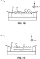
- FIG. 1B shows an example of an optical coupler 101 that may be implemented in the photonic integrated circuit 100.
- the optical coupler 101 may also be implemented in any one of the other photonic integrated circuits described throughout this application, or in another photonic integrated circuit not described in this application.
- the optical coupler 101 includes an interference region 110 and a grating region 120.
- the grating region 120 includes grating valleys 118 and grating peaks 126, which together form a grating having a grating length, L Grating .
- the height difference between a grating peak 126 and a grating valley 118 determines a grating height.
- the ratio of the peak width to the sum of peak width and valley width of the grating along the wave propagation direction determines the duty cycle of the grating.
- the sum of the grating peak width and the grating valley width determines the period of the grating.
- the directionality and far field angle of light emitted/received by the grating region 120 can be determined.
- the grating height and the duty cycle may be modified to optimize the directionality of the light.
- the grating period and the duty cycle may be tuned to achieve the desired far field angles which might be most suitable for a targeted application.
- the height of the grating peaks may be higher than the height of the first reflector region 106 and/or the second reflector region 114.
- the first reflector region 106, the interference region 110, and the second reflector region 114 may be planarized by polishing, and then another layer of material is deposited on the planarized surface so that the grating region 120 may be formed by patterning and etching.
- the height of the grating valleys may be lower than the height of the first reflector region 106 and/or the second reflector region 114.
- FIG. 1C shows an example of an optical coupler 103 where the height of the grating valleys 119 is lower than the height of the first reflector region 106 and the second reflector region 114.
- the first reflector region 106, the interference region 110, and the second reflector region 114 may be planarized by polishing, and then the grating region 120 may be formed on the polished surface by patterning and etching the interference region 110.
- the optical coupler 103 may be implemented in the photonic integrated circuit 100.
- the optical coupler 103 may also be implemented in any one of the other photonic integrated circuits described throughout this application, or in another photonic integrated circuit not described in this application.
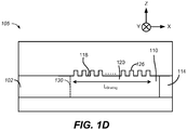
- FIG. 1D shows an example not forming part of the invention of an optical coupler 105 that includes the waveguide region 102, the interference region 110, the grating region 120, and the second reflector region 114, but does not include the first reflector region 106.
- the boundary 130 between the waveguide region 102 and the interference region 110 is denoted by a dashed line 130 because in some implementations, the waveguide region 102 and the interference region 110 are composed of the same material or having substantially equal effective refractive index.
- the optical coupler 105 does not include the first reflector region 106 in the case where light in the interference region 110 is attenuated below a threshold value after propagating one-circulation in the interference region 110.
- a standing wave may be created in the interference region 110 through interference between forward light incident on the second reflector region 114 and backward light reflected by the second reflector region 114.
- the standing wave may diminish near the boundary 130 between the waveguide region 102 and the interference region 110 because the light reflected by the second reflector region 114 is attenuated below the threshold value beyond the boundary 130.
- the threshold value for example, may be less than 10% of the initial incident light power.
- the optical coupler 105 can be used to redirect light propagating along a first direction to a second direction that is different to the first direction without the first reflector region 106.
- the optical coupler 105 may be used to direct light to a second direction that is substantially perpendicular to the first direction.
- the optical coupler can still redirect an incident light with high efficiency if the light is attenuated below a threshold value after propagating one-circulation in the interference region 110.
- the grating region 120 needs to provide enough one-circulation attenuation.
- the grating length L Grating needs to be long enough to provide sufficient one-circulation attenuation before reaching the boundary 130.
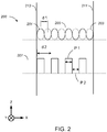
- FIG. 2 is an example of a grating pattern 207 that substantially matches an interference periodicity of the standing wave 205 inside the interference region.
- the descriptions of FIG. 2 may be applied to any one of the optical couplers described in this application.
- the round-trip phase shift is the sum of the phase shift introduced by the one-circulation propagation and the phase shift introduced by a reflector.
- the phase shift introduced by the reflector may be assumed to be zero so that the resonant condition "round-trip phase shift equals 2m ⁇ " can be viewed as the same as “one-circulation phase shift equals 2m ⁇ ," where m is any integer.
- light propagating in a waveguide may be confined by two dimensions.
- light propagating in the waveguide region 102 is confined in y and z dimensions.
- the confinement of the waveguide may be weakened, and the light propagates like a point wave inside the interference region.
- the interference region 110 may be designed to confine light tightly in the z dimension and confine light loosely in the y dimension.
- the point wave reaches a reflector 211, gets reflected, and a standing wave pattern 205 having a periodicity of d1 may be formed inside the interference region through the interference of a forward propagating wave 201 and a backward propagating wave 203.
- an one-circulation attenuation coefficient, ⁇ may be calculated along with a corresponding phase shift for the resonant condition inside the interference region.
- the interference region may be composed of a material that has a specific absorption coefficient for the guided light, which contributes to the one-circulation attenuation coefficient.
- light may be emitted by the grating region during propagation, which also contributes to the one-circulation attenuation coefficient.
- one-circulation attenuation coefficient ⁇ refers to a ratio between the remaining optical power after the one-circulation attenuation and the initial optical power.
- a reflector region (e.g., the first reflector region 106) may be placed at the boundary 213, where the reflectivity of the reflector region at the boundary 213 is configured to substantially match the one-circulation attenuation coefficient ⁇ .
- the one circulation attenuation coefficient ⁇ may be near zero.
- the corresponding reflectivity r at the boundary 213 can be set as zero, which corresponds to the optical coupler 105 in FIG. 1D , where the first reflector region 106 is not included in the optical coupler 105.
- the reflectivity r at the boundary 213 can be set as high as the reflectivity of the reflector 211, (e.g., close to 1), to form a highly confined cavity along the x direction, where the light can enter or leave the cavity through another direction such as in the z direction.
- a change of effective refractive index may occur from the etching of the grating region on the interference region.
- the etching process may not create a straight line from the grating peak to the grating valley.
- slight deviation from the exact condition may be expected during real implementation.
- Such deviation does not change the functionality of the optical coupler, but may affect the efficiency.
- any reasonable deviation from the ideal case is within the scope of this disclosure, where the efficiency is acceptable for a targeted application.
- An iterative process of fabricating the optical coupler, testing the optical coupler, and then re-designing the optical coupler may improve this issue.
- FIG. 3A shows an example of a view of a grating pattern 331 on a plane along the x-y dimensions.
- the descriptions of FIG. 3A may be applied to any one of the optical couplers described in this application.
- the grating pattern 331 includes an array of one-dimensional grating structures 301a-n and 303a-n along the x direction, where n is any integer greater than one.
- the grating structures 301a-n and 303a-n may be composed of different materials.
- the grating structures 301a-n may be composed of silicon
- the grating structures 303a-n may be composed of InP.
- the grating structures 303a-n may include a layer of metal that forms surface plasmonic effect that couples light from an external medium to the interference region.
- the arrangement of 301a, 303a, 301b, 303b, ..., 301n, and 303n forms the grating in a grating region.
- FIG. 3B shows an example of a view of a grating pattern 332 on a plane along the x-y dimensions.
- the descriptions of FIG. 3B may be applied to any one of the optical couplers described in this application.
- the grating pattern 332 includes an array of one-dimensional grating structures 305a-n along the x direction, where n is any integer greater than one.
- the grating structures 305a-n may be grating peaks of a grating.
- the grating structures 305a-n may be grating valleys of a grating.
- the arrangement of 305a, 305b, ..., and 305n forms the grating in a grating region.
- FIG. 3C shows an example of a view of a grating pattern 333 on a plane along the x-y dimensions.
- the descriptions of FIG. 3C may be applied to any one of the optical couplers described in this application.
- the grating pattern 333 includes an array of two-dimensional rectangular grating structures 307a to 307n along the x direction, and 307a to 307k along the y direction.
- the rectangular grating structure 307a may be a grating peak of a grating.
- the rectangular grating structure 307a may be a grating valley of a grating.
- the rectangular grating structure 307a may be composed of the same material as the layer 308, such as silicon.
- the rectangular grating structure 307a may be composed of a different material from the layer 308.
- the rectangular grating structure 307a may be composed of silicon, and the layer 308 may be composed of InP.
- the rectangular grating structure 307a may be a square or a non-square, or combinations of both structures.
- the arrangement of the rectangular grating structures 307a-n and 307a-k on the x-y plane forms the grating in a grating region.
- the period of the grating along the x direction 321 and period of the grating along the y direction 322 substantially match the interference pattern in the layer 308 along the x and y directions, respectively.
- FIG. 3D shows an example of a view of a grating pattern 334 on a plane along the x-y dimensions.
- the descriptions of FIG. 3D may be applied to any one of the optical couplers described in this application.
- the grating pattern 334 includes an array of two-dimensional arbitrary-shaped grating structures 309a to 309n, where n is any integer greater than one.
- the arbitrary-shaped grating structure 309a may be a grating peak of a grating.
- the arbitrary-shaped grating structure 309a may be a grating valley of a grating.
- the arbitrary-shaped grating structure 309a may be composed of a different material from the layer 310.
- the arbitrary-shaped grating structure 309a may be composed of silicon-dioxide, and the layer 308 may be composed of silicon.
- the arbitrary-shaped grating structure 309a may be a triangle or an ellipse or combinations of different shapes. The arrangement of the arbitrary-shaped grating structures 309a-n on the x-y plane forms the grating in a grating region.
- FIG. 3E shows an example of a view of a grating pattern 335 on a plane along the x-y dimensions.
- the descriptions of FIG. 3E may be applied to any one of the optical couplers described in this application.
- the grating pattern 335 includes an array of two-dimensional arbitrary-shaped grating structures 313a to 313n, where n is any integer greater than one.
- the shape of any one of the arbitrary-shaped grating structures 313a to 313n may be determined using numerical analysis. For example, a Finite-difference time-domain (FDTD) analysis program may be used to design the shape of each of the arbitrary-shaped structures 313a to 313n that optimizes the coupling efficiency.
- FDTD Finite-difference time-domain
- the distance between each one of the arbitrary-shaped grating structures 313a to 313n may be determined using numerical analysis. For example, a Finite-difference time-domain (FDTD) analysis program may be used to determine the distance between each one of the arbitrary-shaped structures 313a to 313n that optimizes the coupling efficiency.
- FDTD Finite-difference time-domain
- the arrangement of the arbitrary-shaped grating structures 313a-n on the x-y plane forms the grating in a grating region.
- the two-dimensional gratings shown in Fig. 3C, Fig. 3D, and Fig. 3E can have lattice vectors (which define the unit cell size and shape) designed so that the locations of the in-phase antinodes of the interference region substantially match the locations of grating valleys and/or peaks.
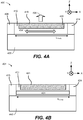
- FIG. 4A shows an example photonic integrated circuit 400 having a grating based optical coupler formed on a light source not forming part of the invention.
- the photonic integrated circuit 400 includes a light source region 430 configured to generate incident light.
- the light source region 430 may generate incoherent light.
- a III-V quantum well laser diode may include one or more layers of active materials that generate incoherent light when pumped with electrical carriers.
- the incoherent light may be coupled to the interference region 410 through spontaneous emission.
- the light source region 430 may be confined at other surfaces except the surface coupled to the interference region 410.
- the optical coupler includes a first reflector region 406, a second reflector region 414, an interference region 410, and a grating region 420.
- the structures of the first reflector region 406, the second reflector region 414, the interference region 410, the grating region 420, and the grating 418 may be implemented by any corresponding structures described throughout this application, for example, the corresponding structures in FIGS. 1A-3E .
- the interference region 410 and the grating region 420 is composed of silicon or III-V materials
- the light source region is composed of III-V materials
- the first and second reflector regions 406 and 414 include DBR structures or metal coating.
- the first reflector region 406 and the second reflector region 414 are configured to reflect incident light at a direction that is opposite to a propagation direction of the incident light as indicated by the arrow 434.
- the interference region 410 is formed between the first reflector region 406 and the second reflector region 414 and is coupled to the light source region 430.
- the interference region 410 may be configured to (i) guide the light generated by the light source region 430 to propagate along a first direction (the x direction in FIG. 4A ), and (ii) confine interference light formed by light reflected between the first reflector region 406 and the second reflector region 414.
- a portion of the light generated in the light source region 430 may be coupled to the interference region 410 through spontaneous emission or any other appropriate coupling mechanism.
- Light coupled to the interference region 410 may resonate along the x direction, as designated by the arrow 434.
- the first reflector region 406 and the second reflector region 414 provide reflective surfaces that forms a cavity in the interference region 410, where a standing wave pattern may be formed. Since the interference region 410 has a fixed cavity length L Cavity , the standing wave pattern can only be formed by certain wavelengths, and the interference region 410 may therefore act as a wavelength filter.
- incoherent light generated by the light source region 430 may be transformed into coherent light in the interference region 410 by filtering out wavelengths that do not resonate in the interference region 410.
- the grating region 420 includes a grating 418 formed on a region confining at least a portion of the interference light.
- the grating 418 is configured to emit a portion of the light at the z direction that is substantially perpendicular to the x direction.
- the grating 418 may be designed and fabricated in the grating region 420 to substantially match the standing wave pattern in the interference region 410. By matching the standing wave pattern, the grating 418 may act as an optical antenna and become the most efficient way for light to leave the interference region 410.
- Each grating structure may act to emit the light as a point wave, and all point-wave fronts emitted from individual grating structures are combined into a planar wave front which propagates in the z direction with low loss.
- FIG. 4B shows an example not forming part of the inventon of a photonic integrated circuit 401 having a grating based optical coupler where a light source region 431 is coupled to the interference region 411 by being embedded in the interference region 411.
- the light source region includes active material layers such as alternating layers of gallium arsenide (GaAs) and aluminum gallium arsenide (GaAlAs) or alternating layers of InGaAsP and InP. Any other combinations of active material layers forming a quantum dot, wire, and well structures that produce incoherent or coherent light are also within the scope of this disclosure.
- the interference region 411 is formed between the first reflector region 416 and the second reflector region 424.
- the first reflector region 416 and the second reflector region 424 may be formed, for example, by coating a metal layer or dielectric layers on the end facets or by forming a DBR structure.
- the light is generated inside the interference region 411.
- the generated light resonates along the x direction between the first reflector region 416 and the second reflector region 424 in the interference region 411 to generate coherent light and form a standing wave pattern.
- the grating region 421 may be designed to substantially match the standing wave pattern, where the coherent light is emitted out of the photonic integrated circuit 401 through the grating region 421 along the z direction.
- the substrate 440 may be used as a supporting layer.
- the substrate 440 may include a DBR structure to further reduce the light that propagates in the -z direction.
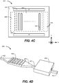
- FIG. 4C shows an example photonic integrated circuit 403 not forming part of the invention having a grating based optical coupler integrated with a light source, where the interference light can be controlled by a p-n junction.
- the photonic integrated circuit 403 includes a light source region 441, a p-doped region 442, an interference region 443, an n-doped region 444, a grating region 445, a first reflector region 446, and a second reflector region 448.
- the structures of the light source region 441, the p-doped region 442, the interference region 443, the n-doped region 444, the grating region 445, the first reflector region 446, and the second reflector region 448 may be implemented by any corresponding structures described throughout this application, for example, the corresponding structures in FIGS. 1A-3E .
- incoherent light is generated in the light source region 441, where a portion of the light is coupled to the interference region 443.
- the coupled light resonates along the x direction between the first reflector region 446 and the second reflector region 448 in the interference region 443 to form a standing wave pattern and generate coherent light.
- a grating in the grating region 445 is designed to substantially match the standing wave pattern, and the coherent light may be emitted out of the photonic integrated circuit 403 through the grating 443 in the +z or -z direction, depending on the design of the grating 445.
- the n-doped region 444 and a p-doped region 442 may be configured to provide an electric field in the interference region 443 with an application of a voltage or a current across the n-doped region 444 and the p-doped region 442.
- the interference region 443 may be configured to provide a different interference pattern with the application of a voltage or a current across the n-doped region 444 and the p-doped region 442 due to the generation, recombination, injection or depletion of free carriers.
- the interference region 443 may stop lasing or may support another lasing wavelength. Therefore the application of a voltage or a current across the n-doped region 444 and the p-doped region 442 can act as a tunable wavelength lasing mechanism or a modulation to the coherent light.
- FIG. 4D shows an example photonic integrated circuit 405 having a light source region coupled to an interference region through a waveguide region where a grating based optical coupler is configured to emit the generated light.
- the photonic integrated circuit 405 includes a light source region 450, a waveguide region 451, a first reflector region 452, a second reflector region 453, an interference region 454, and a grating region 455.
- the structures of the light source region 450, the waveguide region 451, the first reflector region 452, the second reflector region 453, the interference region 454, and the grating region 455 may be implemented by any corresponding structures described throughout this application, for example, the corresponding structures in FIGS. 1A-3E .
- incoherent light is generated in the light source region 450, where a portion of the light is coupled to the waveguide region 451.
- the light source region 450 may include an indium phosphide (InP) quantum well (QW) structure bonded to a silicon waveguide, where the light generated by the QW is coupled to the silicon waveguide.
- the coupled light resonates between the first reflector region 452 and the second reflector region 453 in the interference region 454 to generate coherent light and form a standing wave pattern.
- the waveguide structures of the first reflector region 452 and the second reflector region 453 may be designed to support a single mode propagation, which may filter out higher order modes in the interference region 454.
- a grating in the grating region 455 is designed to substantially match the standing wave pattern, and the coherent light is emitted out of the photonic integrated circuit 405 through the grating region 455 along a direction that is substantially perpendicular to the resonating direction of the light generated by the light source region 450.
- taper regions are used in the interference region to bridge a wider grating region and a narrower waveguide region.
- the narrow waveguide region may be used to suppress high order mode and the wide grating region may be used to match the external coupling device with different beam shapes ,areas and numerical aperture requirement.
- the descriptions of the taper regions may be applied to any one of the optical couplers described in this application.
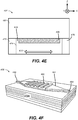
- FIG. 4E shows an example photonic integrated circuit 407 not forming part of the invention having a light source region coupled to a grating based optical coupler through the grating region 466.
- the photonic integrated circuit 407 includes a light source region 462, a first reflector region 478, a second reflector region 476, an interference region 472, a boundary 474, and a grating region 466.
- the structures of the light source region 462, the first reflector region 478, the second reflector region 476, the interference region 472, and the grating region 466 may be implemented by any corresponding structures described throughout this application, for example, the corresponding structures in FIGS. 1A-3E .
- incoherent light is generated in the light source region 462 and coupled to the interference region 472 through spontaneous emission or another suitable coupling mechanism.
- the coupled incoherent light is reflected by the reflector regions 476 and 478, and resonates along the x direction.
- the coherent light when reaching lasing threshold, can emit either in the +z or -z direction depending on the design of the grating region 466.
- the grating region 466 can be designed to direct light mostly to the -z direction so that the emitted light does not couple back to the light source region 462.
- the reflector 478 can be a partial reflector with less reflectivity than the reflector 476.
- the incoherent light generated in the light source region 462 can couple to the interference region 472 through spontaneous emission, and resonates along the direction 470.
- the coherent light can propagate in the -x direction through the boundary 474 into the partial reflector 478 and then into a waveguide, and at the same time propagate in the +z or -z direction into an external medium for further processing.
- FIG. 4F shows an example not forming part of the invention of the photonic circuit 408 having similar layer stacks as FIG. 4B .
- the interference region 491 is composed of active materials such as III-V materials to generate incoherent light.
- the incoherent light resonates between the first reflector 486 and the second reflector 484 along the x direction and becomes coherent.
- the coherent light is emitted through the grating 492 upward since the DBR structure 494 is used to reduce the light that propagates in the downward direction.
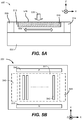
- FIG. 5A shows an example photonic integrated circuit 500 not forming part of the invention having an optical coupler integrated with a light detector.
- the photonic integrated circuit 500 includes an interference region 510, a first reflector region 506, a second reflector region 514, and a grating region 520.
- the interference region 510 includes a light absorption region that is configured to absorb at least a portion of the light in the interference region 510.
- the structures of the interference region 510, the first reflector region 506, the second reflector region 514, and the grating region 520 may be implemented by any corresponding structures described throughout this application, for example, the corresponding structures in FIGS. 1A-3E .
- the photonic integrated circuit 500 may be formed on a substrate 530.
- the grating region 520 includes a grating 518.
- the grating 518 may be configured to receive, from an external medium, light propagating in the direction indicated by the arrow 536.
- Light may be coupled to the interference region 510 formed between the first reflector region 506 and the second reflector region 514.
- the interference region 510 is configured to confine interference light formed by light reflected by the first reflector region 506 and the second reflector region 514 along the direction indicated by the arrow 534.
- the interference region 510 may be composed of a light absorption material that absorbs at least a portion of the interference light.
- the interference region 510 may be composed of germanium that is configured to absorb light in telecommunications wavelengths. The absorbed light is converted to free carriers, which can be collected with an applied electrical field and used to determine an optical power level of the received light.
- light is reflected in a cavity formed by the first reflector region 506 and the second reflector region 514, providing an effective optical absorption.
- the interference region 510 includes silicon and/or germanium for light absorption and the grating region includes metal to create guided surface plasma modes.
- FIG. 5B shows an example photonic integrated circuit 501 not forming part of the invention having a grating based optical coupler integrated with a light detector, where the light detection efficiency can be modulated by a p-n junction.
- the photonic integrated circuit 501 includes an interference region 541, a p-doped region 546, an n-doped region 545, a grating 542, a first reflector region 543, and a second reflector region 544.
- light is received from an external medium, where a portion of the light is coupled to the interference region 541 through the grating 542.
- the coupled light resonates along the x direction between the first reflector region 543 and the second reflector region 544 in the interference region 541.
- the light absorbing material in the interference region 541 absorbs the interference light and coverts the light into free carriers.
- the n-doped region 545 and a p-doped region 546 may be configured to provide an electric field in the interference region 541 with an application of a voltage or a current across the n-doped region 545 and the p-doped region 546.
- the absorption efficiency of the light absorbing material in the interference region 541 may vary based on the application of the voltage or a current across the n-doped region 444 and the p-doped region 442. Therefore the application of a voltage or a current across the n-doped region 444 and the p-doped region 442 acts as a configurable or tunable photo-detector.
- FIG. 5C shows an example photonic integrated circuit 505 having a light absorption region coupled to an interference region through a waveguide region, where a grating based optical coupler is configured to receive light from an external medium.
- the photonic integrated circuit 505 includes a light absorption region 550, a waveguide region 551, a first reflector region 552, a second reflector region 553, an interference region 554, and a grating region 555.
- the structures of the light absorption region 550, the waveguide region 551, the first reflector region 552, the second reflector region 553, the interference region 554, and the grating region 555 may be implemented by any corresponding structures described throughout this application, for example, the corresponding structures in FIGS. 1A-3E .
- light is coupled to the grating region 555 from an external medium.
- the coupled light resonates between the first reflector region 552 and the second reflector region 553 in the interference region 554 to form a standing wave pattern.
- a light absorption region 550 is coupled to the waveguide region 551, and light is coupled from the waveguide region 551 to the light absorption region 550 for detection.
- the light absorption region 550 may be a germanium photo-detector bonded on a silicon waveguide, where light propagating in the silicon waveguide is confined in the interference region 554 and the waveguide region 551, and evanescently coupled to the germanium photo-detector.
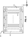
- FIG. 6 shows an example of an optical coupler 600 not forming part of the invention integrated with p-n junctions.
- the optical coupler 600 includes a first reflector region 606, an interference region 620, and a second reflector region 614.
- the interference region 620 includes a grating region 630.
- the first reflector region 606, the interference region 620, the second reflector region 614, and the grating region 630 may be implemented using any one of the corresponding regions as described throughout the application.
- the optical coupler 600 also includes p-n junction pairs including p-doped regions 621, 623, and 625, and n-doped regions 631, 633, and 635.
- p-n junction pairs including p-doped regions 621, 623, and 625, and n-doped regions 631, 633, and 635.
- parameters such as output power and output wavelength may be actively controlled by the application of voltages or carriers injection.
- the p-n junction pairs 621/631, 623/633, and/or 625/635 may extend into the first reflector region 606, the interference region 620, and/or the second reflector region 614, respectively, for better controllability.
- the p-doped and n-doped regions may alternate to form interdigitated patterns or other patterns. The descriptions of the doped regions may be applied to any one of the optical couplers described in this application.
- an n-doped region 631 and a p-doped region 621 may be configured to provide an electric field in the first reflector region 606 with an application of a voltage or a current across the n-doped region 631 and the p-doped region 621, where the first reflector region 606 may be configured to provide a different reflectivity with the application of the voltage or a current across the n-doped region 631 and the p-doped region 621.
- an n-doped region 635 and a p-doped region 625 may be configured to provide an electric field in the second reflector region 614 with an application of a voltage or a current across the n-doped region 635 and the p-doped region 625, wherein the second reflector region 614 may be configured to provide a different reflectivity with the application of a voltage or a current across the n-doped region 635 and the p-doped region 625.
- an n-doped region 633 and a p-doped region 623 may be configured to provide an electric field in the interference region 620 with an application of a voltage or a current across the n-doped region 633 and the p-doped region 623, wherein the interference region 620 may be configured to provide a different interference pattern for the interference light with the application of a voltage or a current across the n-doped region 633 and the p-doped region 623.
- the electric field may extract the free carriers in a region, and therefore may modify the refractive index of the region.
- free carriers may be injected into a region, and therefore may modify the refractive index of the region.
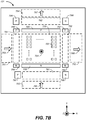
- FIG. 7A shows an example photonic integrated circuit 700 having multiple outputs.
- the photonic integrated circuit 700 includes a first waveguide region 702 configured to guide line in the direction as designated by the arrow 722.
- the photonic integrated circuit 700 includes a first grating region 720 formed on a side of the interference region 710.
- the photonic integrated circuit 700 includes a second grating region 721 formed on a different side of the interference region 710, for example, the opposite side as shown in FIG. 7A .
- the photonic integrated circuit 700 includes a reflector region 714, and may optionally include another reflector region 706.
- the photonic integrated circuit 700 includes a second waveguide region 728 that may be coupled to other passive and/or active optical components.
- light from the first waveguide region 702 enters the interference region 710, and can be directed to a first external medium 730, a second external medium 732, or a second waveguide region 728.
- an n-doped region and a p-doped region may be configured to provide an electric field in the interference region 710 with an application of a voltage or a current across the n-doped region and the p-doped region, where the portion of the light emitted in the +z direction and the portion of the light emitted in the -z direction may be controlled by the application of a voltage or a current across the n-doped region and the p-doped region.
- an n-doped region and a p-doped region may be configured to provide an electric field in the second reflector region 714 with an application of a voltage or a current across the n-doped region and the p-doped region.
- the reflectivity of the second reflector region 714 may be tuned, and light may be transmitted to the second waveguide region 728.
- the light enters the interference region 710, and can be split into different portions of light that exit for the first external medium 730, the second external medium 732, and/or the second waveguide region 728.
- the grating in the first grating region 720 may be designed such that the grating periodicity substantially matches the standing wave of a TE-polarized light.
- the grating in the second grating region 721 may be designed such that the grating periodicity substantially matches the standing wave of a TM-polarized light.
- the portions of light exiting the photonic integrated circuit 700 for the first external medium 730 and the second external medium 732 may be controlled.
- the above example can serve as an effective polarization beam splitter.
- a first layer 724 may be formed between the first grating region 720 and the first external medium 730.
- the first layer 724 may be formed to protect the photonic integrated circuit 700, or to provide a specific distance between the first grating region 720 and the first external medium 730.
- a second layer 716 may be formed between the second grating region 721 and the second external medium 732.
- the second layer 716 may be formed to protect the photonic integrated circuit 700, or to provide a specific distance between the second grating region 721 and the second external medium 732.
- the first layer 724 may be a cladding
- the second layer 716 may be a substrate of the photonic integrated circuit 700.
- the first layer 724 may have a lower refractive index compared to the grating region 720.
- FIG. 7B shows an example photonic integrated circuit 701 having multiple inputs and outputs.
- the photonic integrated circuit 701 may include a first waveguide region 751, a second waveguide region 752, a third waveguide region 753, a fourth waveguide region 754, p-n junctions 755-760 and 795-798, a first reflector region 761, a second reflector region 762, a third reflector region 791, a fourth reflector region 792, an interference region 770, and a two-dimensional grating 780.
- the structures of the first waveguide region 751, the second waveguide region 752, the third waveguide region 753, the fourth waveguide region 754, the p-n junctions 755-760 and 795-798, the first reflector region 761, the second reflector 762, the third reflector region 791, the fourth reflector region 792, the interference region 770, and the two-dimensional grating 780 may be implemented by any corresponding structures described throughout this application, for example, the corresponding structures in FIGS. 1A-6 .
- light from the first and the third waveguide region 751 and 753 enter the interference region 770, and may be directed to the second waveguide region 752, the fourth waveguide region 754, or out of the grating in the z direction as designated by the outward arrow 764.
- the reflectivity of the first and the third reflector regions 761 and 791 can be tuned during the initial design or through dynamic application of electrical field to match the one-circulation attenuation coefficients of the wave propagating along the x and y direction respectively.
- the grating region may include a two-dimensional grating 780 configured to separate light into two light portions propagating along two directions x and y according to wavelengths.
- the grating region may include a two-dimensional grating 780 configured to separate light into two light portions propagating along two directions x and y according to polarization.
- the two-dimensional grating 780 may be configured to reversely combine two light portions propagating along two directions x and y into one light portion.
- the two-dimensional grating 780 may be configured to emit light upward in the z direction by combining two lights coming from two directions x and y, by substantially matching the periods of the grating 780 along the x and y direction to periods of the interference pattern along the x and y directions respectively. In some implementations, the two-dimensional grating 780 may be configured to emit light upward in the z direction by combining two lights coming from two directions x and y, by modifying the interference pattern along the x and y directions, through the application of electrical fields between p-doped and n-doped regions, to match the grating 780 pattern along the x and y directions respectively. As another example, the two-dimensional grating 780 may be configured to reversely split one light propagating at one direction (e.g. -z) into two light portions propagating along two directions x and y.
- one direction e.g. -z
- an n-doped region and a p-doped region may be configured to provide an electric field in the interference region with an application of a voltage or a current across the n-doped region and the p-doped region, where a respective proportion of each of the two light portions propagating along two directions is controlled by the application of a voltage or a current across the n-doped region and the p-doped region.
- a voltage may be applied across the n-doped region 759 and the p-doped region 756 to control the routing or the splitting of the input light.
- one or more doped regions can be eliminated if there is no need to modulate the refractive index of corresponding regions.
- the doped regions 756 and 759 can be eliminated if there is no need to dynamically modulate the interference region 770.
- FIG. 8 shows an example of a photonic integrated circuit 800 suitable for packaging.
- the photonic integrated circuit 800 includes an edge emitting light source 801 that is butt-coupled to a waveguide 803.
- the light may be modulated by optionally including an integrated modulator 805 as shown in FIG. 8 , or through direct modulation of the edge emitting light source 801.
- the modulated light is coupled to a grating-based optical coupler 807 as described in previous figures. Since light emitted by the optical coupler 807 may be designed to emit along a direction that is substantially perpendicular than the direction of light emitted by the edge emitting light source 801, the photonic integrated circuit 800 may be readily tested and packaged with a standardized optical equipment.
- the die where the photonic integrated circuit 800 is fabricated on may be attached to the inside surface of a transistor outline (TO) metal can, where the grating may be aligned to the aperture of the TO metal can, allowing vertical transmission of light out of the package.
- TO transistor outline
- FIG. 9A shows an example of an optical apparatus 901, including a corner mirror 902 that provides a high-reflectivity.
- the descriptions of FIG. 9A may be applied to any one of the reflector regions disclosed in this application.
- light propagates through the grating region 920, and is incident on the facets 931a and 931b of the corner mirror 902. Because the light is incident on the facets 931a and 931b beyond a total reflection angle, substantial light is reflected due to total reflection, achieving a high-reflectivity.
- FIG. 9B shows an example of an optical apparatus 903, including a circular or elliptical facet 904 that provides a partial-reflectivity or a high-reflectivity.
- the descriptions of FIG. 9B may be applied to any one of the reflector regions disclosed in this application.
- light propagates through the curved grating region 921, and is incident on the facet 904.
- the facet 904 may be coated with a metal layer to provide a high-reflectivity.
- the curved facet 904 refocuses the light back toward the direction of the waveguide region by the high-reflectivity curved facet 904.
- FIG. 9C shows an example of an optical apparatus 905, including a distributed Bragg reflector (DBR) mirror 906 providing a high-reflectivity.
- DBR distributed Bragg reflector
- the descriptions of FIG. 9C may be applied to any one of the reflector regions disclosed in this application.
- light propagates through the grating region 922, and is incident on DBR mirror 906.
- the DBR mirror 906 may be designed to provide a high reflectivity for a range of wavelengths.
- FIG. 9D shows an example of an optical apparatus 907, including a facet 908 providing a partial-reflectivity or a high-reflectivity.
- the descriptions of FIG. 9D may be applied to any one of the reflector regions disclosed in this application.
- light propagates through the grating region 923, and is incident on the facet 908. Without any additional coating, the reflectivity may be determined using the Fresnel equations.
- the facet 908 may be coated with one or more layers of materials to increase the reflectivity.
- the facet 908 may be coated with a metal layer to increase the reflectivity.
- the facet 908 may be coated with multiple dielectric layers to increase the reflectivity for a range of wavelengths.
- the facet 908 may be coated with a quarter-wavelength dielectric layer followed by a metal layer to increase the reflectivity for a range of wavelengths.
- FIG. 9E shows an example of an optical apparatus 909, including a surface corrugated mirror 936.
- the descriptions of FIG. 9E may be applied to any one of the reflector regions disclosed in this application.
- light propagates through the grating region 932, and is incident into the mirror 936 and gets reflected, forming an interference pattern.
- a reflector region may alternatively include an anomalously dispersive mirror or a waveguide loop mirror.
- FIG. 10 shows a flow diagram for designing an optical coupler.
- the process 1000 may be performed by data processing apparatus, such as one or more computers.
- the system obtains cavity dimensions (1002).
- the dimensions and materials of the cavity and the substrate can be determined. For example, for a single mode optical signal with center wavelength around 1310nm, a Si layer cavity having a thickness of 250nm on an oxide layer can be used. If the spot size of the external fiber is around 10 ⁇ m, the dimension of the cavity needs to be around or larger than 10 ⁇ m to allow the external fiber to be coupled onto the grating structure.
- the system determines grating dimensions (1004).
- the design of the grating dimensions depends on the standing wave pattern inside the cavity.
- the period of the grating pattern needs to be substantially matched to the standing wave pattern, and the other parameters, such as the duty cycle, and grating height, shape of the grating structure, are other design parameters that may be optimized based on parameters such as the incident light spot size, mode of the light, wavelength of the light, material of the cavity, intended emitting angle, etc.
- the standing wave pattern can be estimated assuming a specific mirror reflectivity.
- the system determines grating characteristics (1006).
- a numerical analysis tool such as a FDTD simulation system can be used to optimize the design parameters until a high directionality and the intended emission angle, for example a substantially vertical emission, are both reached.
- the system determines mirror characteristics (1008).
- a numerical analysis tool such as a FDTD simulation system may optimize design parameters to generate a design for a back mirror having a reflection that is close to 100%.
- the design may be a tapered waveguide distributed Bragg reflector (DBR), a waveguide loop mirror, or a Si-SiO2-metal coating layer.
- DBR distributed Bragg reflector
- Si-SiO2-metal coating layer Si-SiO2-metal coating layer.
- the FDTD simulation system may be used to determine the one-circulation attenuation coefficient ⁇ , as described in FIG. 2 . Based on the calculated one-circulation attenuation coefficient ⁇ , the system may design a front mirror having a reflectivity that substantially matches the one-circulation attenuation coefficient ⁇ . In some implementations, multiple doped regions can be placed near the regions to modify the properties of the regions through the application of electrical field.
- a proper mirror design e.g., tapered DBR or corner mirror or oxide-metal coating, etc.
- grating structure on top of the interference region can be designed based on the initial interference wave pattern.
- the one circulation attenuation coefficient ( ⁇ ) can be determined along with the corresponding phase shift for the resonant condition.
- another mirror or reflector can be added on another side of the interference region.
- FIG. 11 shows a flow diagram for fabricating an optical coupler.
- the process 1100 may be performed by a system including data processing apparatus, such as one or more computers that control one or more apparatuses that perform the fabrication steps.
- the system fabricates gratings (1102).
- the fabrication of gratings may be done by a combination of CMOS compatible fabrication techniques.
- lithography techniques such as projection lithography, electronic-beam lithography, contact lithography, or any other suitable lithography techniques may be used to pattern the gratings.
- etching techniques such as dry etching, wet etching, or any other suitable etching techniques may be used to etch the patterned gratings.
- thin film deposition techniques such as chemical vapor deposition, plasma-enhanced chemical vapor deposition, sputtering, or any other suitable thin film deposition techniques may be used to deposit one or more layers of materials on the gratings.
- the system can also optionally measure grating characteristics (1104) as a mid-process check point.
- the measurement of grating characteristics may be performed on a die level.
- the measurement of grating characteristics may be performed on a wafer level.
- input light is coupled into a photonic integrated circuit through a fabricated grating on the input end, and output light is coupled out of the photonic integrated circuit through another fabricated grating on the output end.
- input light is coupled into a photonic integrated circuit through a fabricated grating, where the light is reflected by a high-reflectivity reflector. The reflected light may be coupled out of the photonic integrated circuit through the same grating, and separated out by an optical circulator.
- the grating characteristics such as the one-circulation attenuation coefficient may be measured and analyzed by comparing the output light with the input light.
- the measurement of grating characteristics may be performed by shining a light at a tilt angle onto the fabricated grating and measure the reflected light at another angle.
- the system fabricates mirrors (1106).
- the system can optimize the parameters for a reflector that matches the one-circulation attenuation coefficient.
- the fabrication of the one or more reflectors may be done by a combination of CMOS compatible fabrication techniques.
- the doped regions can be lithography defined, implanted and activated at locations near the regions needs to be modified through the application of electrical field.
- step 1008 can also be done before step 1004.
- step 1104 can also be done after step 1106.
Landscapes
- Physics & Mathematics (AREA)
- General Physics & Mathematics (AREA)
- Optics & Photonics (AREA)
- Nonlinear Science (AREA)
- Engineering & Computer Science (AREA)
- Microelectronics & Electronic Packaging (AREA)
- Optical Integrated Circuits (AREA)
- Optical Couplings Of Light Guides (AREA)
- Optical Modulation, Optical Deflection, Nonlinear Optics, Optical Demodulation, Optical Logic Elements (AREA)
- Semiconductor Lasers (AREA)
- Optical Elements Other Than Lenses (AREA)
Applications Claiming Priority (7)
| Application Number | Priority Date | Filing Date | Title |
|---|---|---|---|
| US201361895493P | 2013-10-25 | 2013-10-25 | |
| US201461925629P | 2014-01-09 | 2014-01-09 | |
| US201461946657P | 2014-02-28 | 2014-02-28 | |
| US201461979489P | 2014-04-14 | 2014-04-14 | |
| US201462012446P | 2014-06-16 | 2014-06-16 | |
| US201462014182P | 2014-06-19 | 2014-06-19 | |
| US14/510,799 US9239507B2 (en) | 2013-10-25 | 2014-10-09 | Grating based optical coupler |
Publications (2)
| Publication Number | Publication Date |
|---|---|
| EP2866067A1 EP2866067A1 (en) | 2015-04-29 |
| EP2866067B1 true EP2866067B1 (en) | 2020-07-29 |
Family
ID=51753063
Family Applications (1)
| Application Number | Title | Priority Date | Filing Date |
|---|---|---|---|
| EP14189392.5A Active EP2866067B1 (en) | 2013-10-25 | 2014-10-17 | Grating based optical coupler |
Country Status (8)
| Country | Link |
|---|---|
| US (2) | US9239507B2 (enExample) |
| EP (1) | EP2866067B1 (enExample) |
| JP (1) | JP6640445B2 (enExample) |
| KR (1) | KR20150048078A (enExample) |
| CN (2) | CN110275247B (enExample) |
| CA (1) | CA2867951A1 (enExample) |
| SG (1) | SG10201406933YA (enExample) |
| TW (1) | TWI648564B (enExample) |
Families Citing this family (61)
| Publication number | Priority date | Publication date | Assignee | Title |
|---|---|---|---|---|
| US11726332B2 (en) | 2009-04-27 | 2023-08-15 | Digilens Inc. | Diffractive projection apparatus |
| WO2016020630A2 (en) | 2014-08-08 | 2016-02-11 | Milan Momcilo Popovich | Waveguide laser illuminator incorporating a despeckler |
| US9933684B2 (en) | 2012-11-16 | 2018-04-03 | Rockwell Collins, Inc. | Transparent waveguide display providing upper and lower fields of view having a specific light output aperture configuration |
| DE102013212752B4 (de) * | 2013-03-01 | 2024-02-29 | IHP GmbH - Innovations for High Performance Microelectronics/Institut für innovative Mikroelektronik | Integriert-optische Koppler-Vorrichtung zwischen integriert-optischen Wellenleitern und einer optischen Mehrmodenfaser, sowie optoelektronische Vorrichtung und Anordnung mit einer solchen Koppler-Vorrichtung |
| US9239507B2 (en) | 2013-10-25 | 2016-01-19 | Forelux Inc. | Grating based optical coupler |
| US10386581B2 (en) | 2013-10-25 | 2019-08-20 | Forelux Inc. | Grating based optical transmitter |
| US9766410B1 (en) * | 2014-07-11 | 2017-09-19 | Acacia Communications, Inc. | Wafer-level testing of photonic integrated circuits with optical IOs |
| KR20170092522A (ko) * | 2014-09-08 | 2017-08-11 | 더 리서치 파운데이션 포 더 스테이트 유니버시티 오브 뉴욕 | 금속 격자 및 이의 측정 방법 |
| US10241330B2 (en) | 2014-09-19 | 2019-03-26 | Digilens, Inc. | Method and apparatus for generating input images for holographic waveguide displays |
| WO2016113534A1 (en) | 2015-01-12 | 2016-07-21 | Milan Momcilo Popovich | Environmentally isolated waveguide display |
| US9632226B2 (en) | 2015-02-12 | 2017-04-25 | Digilens Inc. | Waveguide grating device |
| WO2016146963A1 (en) * | 2015-03-16 | 2016-09-22 | Popovich, Milan, Momcilo | Waveguide device incorporating a light pipe |
| EP4425153A3 (en) | 2015-06-12 | 2024-11-20 | Pacific Biosciences Of California, Inc. | Integrated target waveguide devices and systems for optical coupling |
| TWI566918B (zh) | 2015-07-29 | 2017-01-21 | 財團法人工業技術研究院 | 立體列印系統 |
| JP6089077B1 (ja) * | 2015-08-25 | 2017-03-01 | 沖電気工業株式会社 | 導波路型光回折格子及び光波長フィルタ |
| KR102640201B1 (ko) * | 2015-08-28 | 2024-02-23 | 삼성전자주식회사 | 페브리-페로 공진기 구조를 포함하는 온칩 광학필터 및 분광기 |
| US9939587B2 (en) * | 2015-08-28 | 2018-04-10 | Samsung Electronics Co., Ltd. | On-chip optical filter comprising Fabri-Perot resonator structure and spectrometer |
| EP3359999A1 (en) | 2015-10-05 | 2018-08-15 | Popovich, Milan Momcilo | Waveguide display |
| US9798084B2 (en) * | 2015-11-20 | 2017-10-24 | Google Inc. | Photonic chip grating couplers |
| US10992104B2 (en) | 2015-12-17 | 2021-04-27 | Ii-Vi Delaware, Inc. | Dual layer grating coupler |
| CN108701962B (zh) | 2015-12-17 | 2021-04-16 | 菲尼萨公司 | 表面耦合系统 |
| US10067303B1 (en) * | 2016-01-14 | 2018-09-04 | Finisar Corporation | Optical grating |
| US11513350B2 (en) | 2016-12-02 | 2022-11-29 | Digilens Inc. | Waveguide device with uniform output illumination |
| WO2018129398A1 (en) | 2017-01-05 | 2018-07-12 | Digilens, Inc. | Wearable heads up displays |
| US10412378B2 (en) | 2017-05-08 | 2019-09-10 | Microsoft Technology Licensing, Llc | Resonating optical waveguide using multiple diffractive optical elements |
| US10222615B2 (en) | 2017-05-26 | 2019-03-05 | Microsoft Technology Licensing, Llc | Optical waveguide with coherent light source |
| US11262605B2 (en) * | 2017-08-31 | 2022-03-01 | Lightwave Logic Inc. | Active region-less polymer modulator integrated on a common PIC platform and method |
| FR3071626B1 (fr) * | 2017-09-26 | 2019-11-01 | Commissariat A L'energie Atomique Et Aux Energies Alternatives | Dispositif de couplage optique pour un circuit photonique. |
| CN107765375B (zh) * | 2017-11-21 | 2019-06-25 | 南京大学 | 基于双层光栅的芯片-光纤垂直耦合结构 |
| JP7145436B2 (ja) * | 2017-12-27 | 2022-10-03 | パナソニックIpマネジメント株式会社 | 光学装置 |
| WO2019136473A1 (en) | 2018-01-08 | 2019-07-11 | Digilens, Inc. | Methods for fabricating optical waveguides |
| KR102768598B1 (ko) | 2018-01-08 | 2025-02-13 | 디지렌즈 인코포레이티드. | 도파관 셀 내의 홀로그래픽 격자의 높은 처리능력의 레코딩을 위한 시스템 및 방법 |
| WO2019159345A1 (ja) * | 2018-02-19 | 2019-08-22 | 三菱電機株式会社 | 半導体光集積デバイス |
| CN108333681B (zh) * | 2018-04-08 | 2023-10-13 | 浙江大学 | 基于部分透射式角反射镜组的片上集成部分反射器 |
| TWI673618B (zh) * | 2018-06-27 | 2019-10-01 | 英業達股份有限公司 | 導光體輔助設計方法 |
| US11435522B2 (en) * | 2018-09-12 | 2022-09-06 | Ii-Vi Delaware, Inc. | Grating coupled laser for Si photonics |
| US10914892B2 (en) * | 2018-10-18 | 2021-02-09 | Cisco Technology, Inc. | Germanium photodetector coupled to a waveguide |
| US10802213B2 (en) * | 2018-12-27 | 2020-10-13 | Juniper Networks, Inc. | Photodetector with sequential asymmetric-width waveguides |
| JP7252598B2 (ja) * | 2019-01-08 | 2023-04-05 | 国立大学法人東京工業大学 | 光機能デバイスの制御方法および制御装置 |
| WO2020149956A1 (en) | 2019-01-14 | 2020-07-23 | Digilens Inc. | Holographic waveguide display with light control layer |
| WO2020163524A1 (en) | 2019-02-05 | 2020-08-13 | Digilens Inc. | Methods for compensating for optical surface nonuniformity |
| US20220283377A1 (en) | 2019-02-15 | 2022-09-08 | Digilens Inc. | Wide Angle Waveguide Display |
| EP3924759B1 (en) | 2019-02-15 | 2025-07-30 | Digilens Inc. | Methods and apparatuses for providing a holographic waveguide display using integrated gratings |
| US11404850B2 (en) | 2019-04-22 | 2022-08-02 | Ii-Vi Delaware, Inc. | Dual grating-coupled lasers |
| CN114207492A (zh) | 2019-06-07 | 2022-03-18 | 迪吉伦斯公司 | 带透射光栅和反射光栅的波导及其生产方法 |
| CN110161600B (zh) * | 2019-07-09 | 2022-08-30 | 京东方科技集团股份有限公司 | 一种阵列基板及其制备方法和液晶显示装置 |
| KR102775783B1 (ko) | 2019-08-29 | 2025-02-28 | 디지렌즈 인코포레이티드. | 진공 격자 및 이의 제조 방법 |
| US11067765B2 (en) | 2019-11-27 | 2021-07-20 | Cisco Technology, Inc. | Evanescent coupling of photodiode with optical waveguide |
| US11378750B2 (en) | 2020-01-17 | 2022-07-05 | Taiwan Semiconductor Manufacturing Company, Ltd. | Germanium photodetector embedded in a multi-mode interferometer |
| WO2021241779A1 (ko) * | 2020-05-28 | 2021-12-02 | 엘지전자 주식회사 | Owc를 위한 주파수 그래디언트 메타서페이스 기반 패스트 빔 스티어링 전송 방법 및 장치 |
| US11204463B1 (en) | 2020-07-17 | 2021-12-21 | Globalfoundries U.S. Inc. | Integrated circuit structure with optical absorber layer over optical grating coupler |
| US11869991B2 (en) * | 2020-09-18 | 2024-01-09 | Taiwan Semiconductor Manufacturing Company Limited | Semiconductor device and method of making |
| EP4020027A1 (en) | 2020-12-23 | 2022-06-29 | EFFECT Photonics B.V. | An environmentally protected photonic integrated circuit |
| CN114675369A (zh) * | 2020-12-24 | 2022-06-28 | 天津大学 | 波导光栅器件、光波导相控阵、光学扫描及光通信装置 |
| WO2022150841A1 (en) | 2021-01-07 | 2022-07-14 | Digilens Inc. | Grating structures for color waveguides |
| US11474294B2 (en) * | 2021-01-29 | 2022-10-18 | Globalfoundries U.S. Inc. | Grating couplers with segments having sections of inverted curvature |
| JP2024508926A (ja) | 2021-03-05 | 2024-02-28 | ディジレンズ インコーポレイテッド | 真空周期的構造体および製造の方法 |
| WO2024125102A1 (zh) * | 2022-12-16 | 2024-06-20 | 上海鲲游科技有限公司 | 二维光栅结构、扩瞳结构、耦出结构以及衍射光波导 |
| EP4459370A1 (en) * | 2023-05-02 | 2024-11-06 | Alpine Quantum Technologies GmbH | Suppression of spontaneous emissions |
| CN116908991B (zh) * | 2023-07-18 | 2025-07-29 | 河南皓泽电子股份有限公司 | 棱镜镜头一体式驱动装置 |
| WO2025238847A1 (ja) * | 2024-05-17 | 2025-11-20 | Ntt株式会社 | 半導体レーザ |
Citations (1)
| Publication number | Priority date | Publication date | Assignee | Title |
|---|---|---|---|---|
| US20020136259A1 (en) * | 2001-03-05 | 2002-09-26 | Photodigm. Inc. | Optical modulator system |
Family Cites Families (29)
| Publication number | Priority date | Publication date | Assignee | Title |
|---|---|---|---|---|
| JP2692913B2 (ja) | 1987-12-19 | 1997-12-17 | 株式会社東芝 | グレーティング結合型表面発光レーザ素子およびその変調方法 |
| US5038185A (en) | 1989-11-30 | 1991-08-06 | Xerox Corporation | Structurally consistent surface skimming hetero-transverse junction lasers and lateral heterojunction bipolar transistors |
| US6104852A (en) * | 1996-01-18 | 2000-08-15 | British Telecommunications Public Limited Company | Optical waveguide with photosensitive refractive index cladding |
| US6031243A (en) | 1996-10-16 | 2000-02-29 | Geoff W. Taylor | Grating coupled vertical cavity optoelectronic devices |
| JPH10178165A (ja) * | 1996-12-19 | 1998-06-30 | Furukawa Electric Co Ltd:The | 感度可変型光集積素子 |
| JPH11281829A (ja) * | 1998-03-31 | 1999-10-15 | Minolta Co Ltd | 光導波路デバイス及びその製造方法 |
| JP3647656B2 (ja) * | 1998-11-05 | 2005-05-18 | 株式会社東芝 | 光機能素子及び光通信装置 |
| JP2004505294A (ja) * | 2000-07-21 | 2004-02-19 | マイクロ マネージド フォトンズ アクティーゼルスカブ | 表面プラズモン・ポラリトン・バンドギャップ構造 |
| US6775427B2 (en) * | 2001-03-09 | 2004-08-10 | Photodigm, Inc. | Laterally coupled wave guides |
| US20040114642A1 (en) | 2002-03-22 | 2004-06-17 | Bullington Jeff A. | Laser diode with output fiber feedback |
| US6970488B2 (en) | 2002-10-16 | 2005-11-29 | Eastman Kodak Company | Tunable organic VCSEL system |
| JP2005159002A (ja) * | 2003-11-26 | 2005-06-16 | Seiko Epson Corp | 受光素子、光モジュール、及び光伝送装置 |
| JP4793820B2 (ja) * | 2006-03-20 | 2011-10-12 | 国立大学法人京都大学 | 2次元フォトニック結晶面発光レーザ光源 |
| JP4772585B2 (ja) * | 2006-05-10 | 2011-09-14 | 浜松ホトニクス株式会社 | 光検出器 |
| US7643709B2 (en) | 2006-05-12 | 2010-01-05 | Interuniversitair Microelektronica Centrum (Imec) | Slanted segmented coupler |
| KR100910979B1 (ko) * | 2007-07-27 | 2009-08-05 | (주)켐옵틱스 | 폴리머 광 도파로형 파장가변 레이저 모듈 |
| CN102047160B (zh) * | 2008-05-19 | 2014-11-19 | Imec公司 | 集成光子器件 |
| JP2009288718A (ja) * | 2008-05-30 | 2009-12-10 | Kyoto Institute Of Technology | 共振グレーティングカップラ |
| CN101793998A (zh) * | 2010-03-10 | 2010-08-04 | 中国科学院半导体研究所 | 带有分布布拉格反射镜的波导光栅耦合器及其制作方法 |
| CN101915965B (zh) * | 2010-08-23 | 2013-11-06 | 清华大学 | 光栅耦合器及其封装结构 |
| US8270791B2 (en) | 2010-10-05 | 2012-09-18 | Tdk Corporation | Optical waveguide and thermally-assisted magnetic recording head therewith |
| US10078190B2 (en) * | 2010-12-20 | 2018-09-18 | Alcatel Lucent | Multi-core optical cable to photonic circuit coupler |
| WO2013089755A1 (en) | 2011-12-15 | 2013-06-20 | Intel Corporation | An efficient backside-emitting/collecting grating coupler |
| CN102565955B (zh) * | 2012-01-16 | 2013-03-20 | 中国科学院半导体研究所 | 电可调谐光栅耦合器 |
| JP5884532B2 (ja) * | 2012-02-06 | 2016-03-15 | 三菱電機株式会社 | フォトダイオード、波長センサ、波長測定装置 |
| EP2634605B1 (en) | 2012-02-29 | 2015-10-28 | Huawei Technologies Co., Ltd. | A diffractive coupling grating for perpendicular coupling |
| CN103197386B (zh) * | 2013-04-01 | 2015-05-20 | 北京工业大学 | 一种金属键合的垂直耦合光栅耦合器及其制作方法 |
| US9239507B2 (en) | 2013-10-25 | 2016-01-19 | Forelux Inc. | Grating based optical coupler |
| US20150117817A1 (en) * | 2013-10-25 | 2015-04-30 | Forelux Inc. | Optical device for redirecting incident electromagnetic wave |
-
2014
- 2014-10-09 US US14/510,799 patent/US9239507B2/en active Active
- 2014-10-17 EP EP14189392.5A patent/EP2866067B1/en active Active
- 2014-10-22 CA CA 2867951 patent/CA2867951A1/en not_active Abandoned
- 2014-10-23 TW TW103136711A patent/TWI648564B/zh active
- 2014-10-23 JP JP2014216265A patent/JP6640445B2/ja active Active
- 2014-10-24 KR KR1020140145457A patent/KR20150048078A/ko not_active Withdrawn
- 2014-10-24 CN CN201910419195.6A patent/CN110275247B/zh active Active
- 2014-10-24 SG SG10201406933YA patent/SG10201406933YA/en unknown
- 2014-10-24 CN CN201410579585.7A patent/CN104570203B/zh active Active
-
2015
- 2015-12-10 US US14/964,865 patent/US9703043B2/en active Active
Patent Citations (1)
| Publication number | Priority date | Publication date | Assignee | Title |
|---|---|---|---|---|
| US20020136259A1 (en) * | 2001-03-05 | 2002-09-26 | Photodigm. Inc. | Optical modulator system |
Non-Patent Citations (1)
| Title |
|---|
| TAILLAERT D ET AL: "AN OUT-OF-PLANE GRATING COUPLER FOR EFFICIENT BUTT-COUPLING BETWEEN COMPACT PLANAR WAVEGUIDES AND SINGLE-MODE FIBERS", IEEE JOURNAL OF QUANTUM ELECTRONICS, IEEE SERVICE CENTER, PISCATAWAY, NJ, USA, vol. 38, no. 7, 1 July 2002 (2002-07-01), pages 949 - 955, XP001169039, ISSN: 0018-9197, DOI: 10.1109/JQE.2002.1017613 * |
Also Published As
| Publication number | Publication date |
|---|---|
| CA2867951A1 (en) | 2015-04-25 |
| CN104570203A (zh) | 2015-04-29 |
| TW201530206A (zh) | 2015-08-01 |
| CN110275247B (zh) | 2024-04-16 |
| US9703043B2 (en) | 2017-07-11 |
| JP6640445B2 (ja) | 2020-02-05 |
| KR20150048078A (ko) | 2015-05-06 |
| JP2015111255A (ja) | 2015-06-18 |
| US9239507B2 (en) | 2016-01-19 |
| SG10201406933YA (en) | 2015-05-28 |
| CN104570203B (zh) | 2019-08-27 |
| EP2866067A1 (en) | 2015-04-29 |
| CN110275247A (zh) | 2019-09-24 |
| TWI648564B (zh) | 2019-01-21 |
| US20160147019A1 (en) | 2016-05-26 |
| US20150117808A1 (en) | 2015-04-30 |
Similar Documents
| Publication | Publication Date | Title |
|---|---|---|
| EP2866067B1 (en) | Grating based optical coupler | |
| EP2913902B1 (en) | Grating based optical transmitter | |
| US6975664B1 (en) | Article comprising a two-dimensional photonic crystal coupler and method of making the same | |
| JP2015111255A5 (enExample) | ||
| JP6020601B2 (ja) | レーザ装置、光変調装置及び光半導体素子 | |
| US10386581B2 (en) | Grating based optical transmitter | |
| US10992104B2 (en) | Dual layer grating coupler | |
| US20170207600A1 (en) | 3d photonic integration with light coupling elements | |
| CN110492350A (zh) | 光接收系统和接收光信号的方法 | |
| US9995876B2 (en) | Configurable compact photonic platforms | |
| JP2009288718A (ja) | 共振グレーティングカップラ | |
| US9548589B2 (en) | Grating based optical transmitter | |
| US20210063779A1 (en) | Magneto-optical waveguide device and coupling methods | |
| Van Thourhout et al. | Coupling mechanisms for a heterogeneous silicon nanowire platform | |
| CN110301075B (zh) | 基于光栅的光发射机 | |
| US20240055829A1 (en) | Semiconductor Laser and Design Method Therefor | |
| Tsunemi et al. | Analysis of optical output characteristics in waveguide coupled HCG-VCSELs |
Legal Events
| Date | Code | Title | Description |
|---|---|---|---|
| PUAI | Public reference made under article 153(3) epc to a published international application that has entered the european phase |
Free format text: ORIGINAL CODE: 0009012 |
|
| 17P | Request for examination filed |
Effective date: 20141017 |
|
| AK | Designated contracting states |
Kind code of ref document: A1 Designated state(s): AL AT BE BG CH CY CZ DE DK EE ES FI FR GB GR HR HU IE IS IT LI LT LU LV MC MK MT NL NO PL PT RO RS SE SI SK SM TR |
|
| AX | Request for extension of the european patent |
Extension state: BA ME |
|
| R17P | Request for examination filed (corrected) |
Effective date: 20151020 |
|
| RBV | Designated contracting states (corrected) |
Designated state(s): AL AT BE BG CH CY CZ DE DK EE ES FI FR GB GR HR HU IE IS IT LI LT LU LV MC MK MT NL NO PL PT RO RS SE SI SK SM TR |
|
| STAA | Information on the status of an ep patent application or granted ep patent |
Free format text: STATUS: EXAMINATION IS IN PROGRESS |
|
| 17Q | First examination report despatched |
Effective date: 20180625 |
|
| GRAP | Despatch of communication of intention to grant a patent |
Free format text: ORIGINAL CODE: EPIDOSNIGR1 |
|
| STAA | Information on the status of an ep patent application or granted ep patent |
Free format text: STATUS: GRANT OF PATENT IS INTENDED |
|
| INTG | Intention to grant announced |
Effective date: 20200218 |
|
| GRAS | Grant fee paid |
Free format text: ORIGINAL CODE: EPIDOSNIGR3 |
|
| GRAA | (expected) grant |
Free format text: ORIGINAL CODE: 0009210 |
|
| STAA | Information on the status of an ep patent application or granted ep patent |
Free format text: STATUS: THE PATENT HAS BEEN GRANTED |
|
| AK | Designated contracting states |
Kind code of ref document: B1 Designated state(s): AL AT BE BG CH CY CZ DE DK EE ES FI FR GB GR HR HU IE IS IT LI LT LU LV MC MK MT NL NO PL PT RO RS SE SI SK SM TR |
|
| REG | Reference to a national code |
Ref country code: CH Ref legal event code: EP |
|
| REG | Reference to a national code |
Ref country code: AT Ref legal event code: REF Ref document number: 1296456 Country of ref document: AT Kind code of ref document: T Effective date: 20200815 |
|
| REG | Reference to a national code |
Ref country code: IE Ref legal event code: FG4D |
|
| REG | Reference to a national code |
Ref country code: DE Ref legal event code: R096 Ref document number: 602014068222 Country of ref document: DE |
|
| REG | Reference to a national code |
Ref country code: LT Ref legal event code: MG4D |
|
| REG | Reference to a national code |
Ref country code: NL Ref legal event code: MP Effective date: 20200729 |
|
| REG | Reference to a national code |
Ref country code: AT Ref legal event code: MK05 Ref document number: 1296456 Country of ref document: AT Kind code of ref document: T Effective date: 20200729 |
|
| PG25 | Lapsed in a contracting state [announced via postgrant information from national office to epo] |
Ref country code: PT Free format text: LAPSE BECAUSE OF FAILURE TO SUBMIT A TRANSLATION OF THE DESCRIPTION OR TO PAY THE FEE WITHIN THE PRESCRIBED TIME-LIMIT Effective date: 20201130 Ref country code: FI Free format text: LAPSE BECAUSE OF FAILURE TO SUBMIT A TRANSLATION OF THE DESCRIPTION OR TO PAY THE FEE WITHIN THE PRESCRIBED TIME-LIMIT Effective date: 20200729 Ref country code: NO Free format text: LAPSE BECAUSE OF FAILURE TO SUBMIT A TRANSLATION OF THE DESCRIPTION OR TO PAY THE FEE WITHIN THE PRESCRIBED TIME-LIMIT Effective date: 20201029 Ref country code: AT Free format text: LAPSE BECAUSE OF FAILURE TO SUBMIT A TRANSLATION OF THE DESCRIPTION OR TO PAY THE FEE WITHIN THE PRESCRIBED TIME-LIMIT Effective date: 20200729 Ref country code: LT Free format text: LAPSE BECAUSE OF FAILURE TO SUBMIT A TRANSLATION OF THE DESCRIPTION OR TO PAY THE FEE WITHIN THE PRESCRIBED TIME-LIMIT Effective date: 20200729 Ref country code: BG Free format text: LAPSE BECAUSE OF FAILURE TO SUBMIT A TRANSLATION OF THE DESCRIPTION OR TO PAY THE FEE WITHIN THE PRESCRIBED TIME-LIMIT Effective date: 20201029 Ref country code: SE Free format text: LAPSE BECAUSE OF FAILURE TO SUBMIT A TRANSLATION OF THE DESCRIPTION OR TO PAY THE FEE WITHIN THE PRESCRIBED TIME-LIMIT Effective date: 20200729 Ref country code: ES Free format text: LAPSE BECAUSE OF FAILURE TO SUBMIT A TRANSLATION OF THE DESCRIPTION OR TO PAY THE FEE WITHIN THE PRESCRIBED TIME-LIMIT Effective date: 20200729 Ref country code: GR Free format text: LAPSE BECAUSE OF FAILURE TO SUBMIT A TRANSLATION OF THE DESCRIPTION OR TO PAY THE FEE WITHIN THE PRESCRIBED TIME-LIMIT Effective date: 20201030 Ref country code: HR Free format text: LAPSE BECAUSE OF FAILURE TO SUBMIT A TRANSLATION OF THE DESCRIPTION OR TO PAY THE FEE WITHIN THE PRESCRIBED TIME-LIMIT Effective date: 20200729 |
|
| PGFP | Annual fee paid to national office [announced via postgrant information from national office to epo] |
Ref country code: GB Payment date: 20201027 Year of fee payment: 7 Ref country code: FR Payment date: 20201026 Year of fee payment: 7 Ref country code: DE Payment date: 20201028 Year of fee payment: 7 |
|
| PG25 | Lapsed in a contracting state [announced via postgrant information from national office to epo] |
Ref country code: PL Free format text: LAPSE BECAUSE OF FAILURE TO SUBMIT A TRANSLATION OF THE DESCRIPTION OR TO PAY THE FEE WITHIN THE PRESCRIBED TIME-LIMIT Effective date: 20200729 Ref country code: LV Free format text: LAPSE BECAUSE OF FAILURE TO SUBMIT A TRANSLATION OF THE DESCRIPTION OR TO PAY THE FEE WITHIN THE PRESCRIBED TIME-LIMIT Effective date: 20200729 Ref country code: RS Free format text: LAPSE BECAUSE OF FAILURE TO SUBMIT A TRANSLATION OF THE DESCRIPTION OR TO PAY THE FEE WITHIN THE PRESCRIBED TIME-LIMIT Effective date: 20200729 Ref country code: IS Free format text: LAPSE BECAUSE OF FAILURE TO SUBMIT A TRANSLATION OF THE DESCRIPTION OR TO PAY THE FEE WITHIN THE PRESCRIBED TIME-LIMIT Effective date: 20201129 |
|
| PG25 | Lapsed in a contracting state [announced via postgrant information from national office to epo] |
Ref country code: NL Free format text: LAPSE BECAUSE OF FAILURE TO SUBMIT A TRANSLATION OF THE DESCRIPTION OR TO PAY THE FEE WITHIN THE PRESCRIBED TIME-LIMIT Effective date: 20200729 |
|
| PG25 | Lapsed in a contracting state [announced via postgrant information from national office to epo] |
Ref country code: IT Free format text: LAPSE BECAUSE OF FAILURE TO SUBMIT A TRANSLATION OF THE DESCRIPTION OR TO PAY THE FEE WITHIN THE PRESCRIBED TIME-LIMIT Effective date: 20200729 Ref country code: DK Free format text: LAPSE BECAUSE OF FAILURE TO SUBMIT A TRANSLATION OF THE DESCRIPTION OR TO PAY THE FEE WITHIN THE PRESCRIBED TIME-LIMIT Effective date: 20200729 Ref country code: EE Free format text: LAPSE BECAUSE OF FAILURE TO SUBMIT A TRANSLATION OF THE DESCRIPTION OR TO PAY THE FEE WITHIN THE PRESCRIBED TIME-LIMIT Effective date: 20200729 Ref country code: CZ Free format text: LAPSE BECAUSE OF FAILURE TO SUBMIT A TRANSLATION OF THE DESCRIPTION OR TO PAY THE FEE WITHIN THE PRESCRIBED TIME-LIMIT Effective date: 20200729 Ref country code: RO Free format text: LAPSE BECAUSE OF FAILURE TO SUBMIT A TRANSLATION OF THE DESCRIPTION OR TO PAY THE FEE WITHIN THE PRESCRIBED TIME-LIMIT Effective date: 20200729 Ref country code: SM Free format text: LAPSE BECAUSE OF FAILURE TO SUBMIT A TRANSLATION OF THE DESCRIPTION OR TO PAY THE FEE WITHIN THE PRESCRIBED TIME-LIMIT Effective date: 20200729 |
|
| REG | Reference to a national code |
Ref country code: DE Ref legal event code: R097 Ref document number: 602014068222 Country of ref document: DE |
|
| PG25 | Lapsed in a contracting state [announced via postgrant information from national office to epo] |
Ref country code: AL Free format text: LAPSE BECAUSE OF FAILURE TO SUBMIT A TRANSLATION OF THE DESCRIPTION OR TO PAY THE FEE WITHIN THE PRESCRIBED TIME-LIMIT Effective date: 20200729 |
|
| REG | Reference to a national code |
Ref country code: CH Ref legal event code: PL |
|
| PLBE | No opposition filed within time limit |
Free format text: ORIGINAL CODE: 0009261 |
|
| STAA | Information on the status of an ep patent application or granted ep patent |
Free format text: STATUS: NO OPPOSITION FILED WITHIN TIME LIMIT |
|
| PG25 | Lapsed in a contracting state [announced via postgrant information from national office to epo] |
Ref country code: MC Free format text: LAPSE BECAUSE OF FAILURE TO SUBMIT A TRANSLATION OF THE DESCRIPTION OR TO PAY THE FEE WITHIN THE PRESCRIBED TIME-LIMIT Effective date: 20200729 Ref country code: LU Free format text: LAPSE BECAUSE OF NON-PAYMENT OF DUE FEES Effective date: 20201017 Ref country code: SK Free format text: LAPSE BECAUSE OF FAILURE TO SUBMIT A TRANSLATION OF THE DESCRIPTION OR TO PAY THE FEE WITHIN THE PRESCRIBED TIME-LIMIT Effective date: 20200729 |
|
| 26N | No opposition filed |
Effective date: 20210430 |
|
| REG | Reference to a national code |
Ref country code: BE Ref legal event code: MM Effective date: 20201031 |
|
| PG25 | Lapsed in a contracting state [announced via postgrant information from national office to epo] |
Ref country code: LI Free format text: LAPSE BECAUSE OF NON-PAYMENT OF DUE FEES Effective date: 20201031 Ref country code: SI Free format text: LAPSE BECAUSE OF FAILURE TO SUBMIT A TRANSLATION OF THE DESCRIPTION OR TO PAY THE FEE WITHIN THE PRESCRIBED TIME-LIMIT Effective date: 20200729 Ref country code: BE Free format text: LAPSE BECAUSE OF NON-PAYMENT OF DUE FEES Effective date: 20201031 Ref country code: CH Free format text: LAPSE BECAUSE OF NON-PAYMENT OF DUE FEES Effective date: 20201031 |
|
| PG25 | Lapsed in a contracting state [announced via postgrant information from national office to epo] |
Ref country code: IE Free format text: LAPSE BECAUSE OF NON-PAYMENT OF DUE FEES Effective date: 20201017 |
|
| REG | Reference to a national code |
Ref country code: DE Ref legal event code: R119 Ref document number: 602014068222 Country of ref document: DE |
|
| PG25 | Lapsed in a contracting state [announced via postgrant information from national office to epo] |
Ref country code: TR Free format text: LAPSE BECAUSE OF FAILURE TO SUBMIT A TRANSLATION OF THE DESCRIPTION OR TO PAY THE FEE WITHIN THE PRESCRIBED TIME-LIMIT Effective date: 20200729 Ref country code: MT Free format text: LAPSE BECAUSE OF FAILURE TO SUBMIT A TRANSLATION OF THE DESCRIPTION OR TO PAY THE FEE WITHIN THE PRESCRIBED TIME-LIMIT Effective date: 20200729 Ref country code: CY Free format text: LAPSE BECAUSE OF FAILURE TO SUBMIT A TRANSLATION OF THE DESCRIPTION OR TO PAY THE FEE WITHIN THE PRESCRIBED TIME-LIMIT Effective date: 20200729 |
|
| GBPC | Gb: european patent ceased through non-payment of renewal fee |
Effective date: 20211017 |
|
| PG25 | Lapsed in a contracting state [announced via postgrant information from national office to epo] |
Ref country code: MK Free format text: LAPSE BECAUSE OF FAILURE TO SUBMIT A TRANSLATION OF THE DESCRIPTION OR TO PAY THE FEE WITHIN THE PRESCRIBED TIME-LIMIT Effective date: 20200729 |
|
| PG25 | Lapsed in a contracting state [announced via postgrant information from national office to epo] |
Ref country code: GB Free format text: LAPSE BECAUSE OF NON-PAYMENT OF DUE FEES Effective date: 20211017 Ref country code: DE Free format text: LAPSE BECAUSE OF NON-PAYMENT OF DUE FEES Effective date: 20220503 |
|
| PG25 | Lapsed in a contracting state [announced via postgrant information from national office to epo] |
Ref country code: FR Free format text: LAPSE BECAUSE OF NON-PAYMENT OF DUE FEES Effective date: 20211031 |