EP2833412A2 - Galliumnitridbasierte Schottky-Diode und Verfahren zur Herstellung davon - Google Patents
Galliumnitridbasierte Schottky-Diode und Verfahren zur Herstellung davon Download PDFInfo
- Publication number
- EP2833412A2 EP2833412A2 EP14179127.7A EP14179127A EP2833412A2 EP 2833412 A2 EP2833412 A2 EP 2833412A2 EP 14179127 A EP14179127 A EP 14179127A EP 2833412 A2 EP2833412 A2 EP 2833412A2
- Authority
- EP
- European Patent Office
- Prior art keywords
- gan
- based semiconductor
- semiconductor layer
- electrode
- layers
- Prior art date
- Legal status (The legal status is an assumption and is not a legal conclusion. Google has not performed a legal analysis and makes no representation as to the accuracy of the status listed.)
- Withdrawn
Links
Images



Classifications
-
- H—ELECTRICITY
- H10—SEMICONDUCTOR DEVICES; ELECTRIC SOLID-STATE DEVICES NOT OTHERWISE PROVIDED FOR
- H10D—INORGANIC ELECTRIC SEMICONDUCTOR DEVICES
- H10D30/00—Field-effect transistors [FET]
- H10D30/60—Insulated-gate field-effect transistors [IGFET]
- H10D30/67—Thin-film transistors [TFT]
- H10D30/6729—Thin-film transistors [TFT] characterised by the electrodes
- H10D30/6737—Thin-film transistors [TFT] characterised by the electrodes characterised by the electrode materials
- H10D30/6738—Schottky barrier electrodes
-
- H—ELECTRICITY
- H10—SEMICONDUCTOR DEVICES; ELECTRIC SOLID-STATE DEVICES NOT OTHERWISE PROVIDED FOR
- H10D—INORGANIC ELECTRIC SEMICONDUCTOR DEVICES
- H10D30/00—Field-effect transistors [FET]
- H10D30/60—Insulated-gate field-effect transistors [IGFET]
- H10D30/67—Thin-film transistors [TFT]
- H10D30/674—Thin-film transistors [TFT] characterised by the active materials
- H10D30/675—Group III-V materials, Group II-VI materials, Group IV-VI materials, selenium or tellurium
-
- H—ELECTRICITY
- H10—SEMICONDUCTOR DEVICES; ELECTRIC SOLID-STATE DEVICES NOT OTHERWISE PROVIDED FOR
- H10D—INORGANIC ELECTRIC SEMICONDUCTOR DEVICES
- H10D62/00—Semiconductor bodies, or regions thereof, of devices having potential barriers
- H10D62/10—Shapes, relative sizes or dispositions of the regions of the semiconductor bodies; Shapes of the semiconductor bodies
- H10D62/102—Constructional design considerations for preventing surface leakage or controlling electric field concentration
- H10D62/103—Constructional design considerations for preventing surface leakage or controlling electric field concentration for increasing or controlling the breakdown voltage of reverse-biased devices
- H10D62/105—Constructional design considerations for preventing surface leakage or controlling electric field concentration for increasing or controlling the breakdown voltage of reverse-biased devices by having particular doping profiles, shapes or arrangements of PN junctions; by having supplementary regions, e.g. junction termination extension [JTE]
- H10D62/106—Constructional design considerations for preventing surface leakage or controlling electric field concentration for increasing or controlling the breakdown voltage of reverse-biased devices by having particular doping profiles, shapes or arrangements of PN junctions; by having supplementary regions, e.g. junction termination extension [JTE] having supplementary regions doped oppositely to or in rectifying contact with regions of the semiconductor bodies, e.g. guard rings with PN or Schottky junctions
-
- H—ELECTRICITY
- H10—SEMICONDUCTOR DEVICES; ELECTRIC SOLID-STATE DEVICES NOT OTHERWISE PROVIDED FOR
- H10D—INORGANIC ELECTRIC SEMICONDUCTOR DEVICES
- H10D62/00—Semiconductor bodies, or regions thereof, of devices having potential barriers
- H10D62/10—Shapes, relative sizes or dispositions of the regions of the semiconductor bodies; Shapes of the semiconductor bodies
- H10D62/113—Isolations within a component, i.e. internal isolations
- H10D62/115—Dielectric isolations, e.g. air gaps
-
- H—ELECTRICITY
- H10—SEMICONDUCTOR DEVICES; ELECTRIC SOLID-STATE DEVICES NOT OTHERWISE PROVIDED FOR
- H10D—INORGANIC ELECTRIC SEMICONDUCTOR DEVICES
- H10D62/00—Semiconductor bodies, or regions thereof, of devices having potential barriers
- H10D62/10—Shapes, relative sizes or dispositions of the regions of the semiconductor bodies; Shapes of the semiconductor bodies
- H10D62/129—Cathode regions of diodes
-
- H—ELECTRICITY
- H10—SEMICONDUCTOR DEVICES; ELECTRIC SOLID-STATE DEVICES NOT OTHERWISE PROVIDED FOR
- H10D—INORGANIC ELECTRIC SEMICONDUCTOR DEVICES
- H10D62/00—Semiconductor bodies, or regions thereof, of devices having potential barriers
- H10D62/80—Semiconductor bodies, or regions thereof, of devices having potential barriers characterised by the materials
- H10D62/85—Semiconductor bodies, or regions thereof, of devices having potential barriers characterised by the materials being Group III-V materials, e.g. GaAs
- H10D62/8503—Nitride Group III-V materials, e.g. AlN or GaN
-
- H—ELECTRICITY
- H10—SEMICONDUCTOR DEVICES; ELECTRIC SOLID-STATE DEVICES NOT OTHERWISE PROVIDED FOR
- H10D—INORGANIC ELECTRIC SEMICONDUCTOR DEVICES
- H10D64/00—Electrodes of devices having potential barriers
- H10D64/60—Electrodes characterised by their materials
- H10D64/64—Electrodes comprising a Schottky barrier to a semiconductor
-
- H—ELECTRICITY
- H10—SEMICONDUCTOR DEVICES; ELECTRIC SOLID-STATE DEVICES NOT OTHERWISE PROVIDED FOR
- H10D—INORGANIC ELECTRIC SEMICONDUCTOR DEVICES
- H10D8/00—Diodes
- H10D8/01—Manufacture or treatment
- H10D8/051—Manufacture or treatment of Schottky diodes
-
- H—ELECTRICITY
- H10—SEMICONDUCTOR DEVICES; ELECTRIC SOLID-STATE DEVICES NOT OTHERWISE PROVIDED FOR
- H10D—INORGANIC ELECTRIC SEMICONDUCTOR DEVICES
- H10D8/00—Diodes
- H10D8/60—Schottky-barrier diodes
-
- H—ELECTRICITY
- H10—SEMICONDUCTOR DEVICES; ELECTRIC SOLID-STATE DEVICES NOT OTHERWISE PROVIDED FOR
- H10P—GENERIC PROCESSES OR APPARATUS FOR THE MANUFACTURE OR TREATMENT OF DEVICES COVERED BY CLASS H10
- H10P14/00—Formation of materials, e.g. in the shape of layers or pillars
- H10P14/20—Formation of materials, e.g. in the shape of layers or pillars of semiconductor materials
- H10P14/27—Formation of materials, e.g. in the shape of layers or pillars of semiconductor materials using selective deposition, e.g. simultaneous growth of monocrystalline and non-monocrystalline semiconductor materials
- H10P14/276—Lateral overgrowth
-
- H—ELECTRICITY
- H10—SEMICONDUCTOR DEVICES; ELECTRIC SOLID-STATE DEVICES NOT OTHERWISE PROVIDED FOR
- H10P—GENERIC PROCESSES OR APPARATUS FOR THE MANUFACTURE OR TREATMENT OF DEVICES COVERED BY CLASS H10
- H10P14/00—Formation of materials, e.g. in the shape of layers or pillars
- H10P14/20—Formation of materials, e.g. in the shape of layers or pillars of semiconductor materials
- H10P14/29—Formation of materials, e.g. in the shape of layers or pillars of semiconductor materials characterised by the substrates
- H10P14/2901—Materials
- H10P14/2921—Materials being crystalline insulating materials
-
- H—ELECTRICITY
- H10—SEMICONDUCTOR DEVICES; ELECTRIC SOLID-STATE DEVICES NOT OTHERWISE PROVIDED FOR
- H10P—GENERIC PROCESSES OR APPARATUS FOR THE MANUFACTURE OR TREATMENT OF DEVICES COVERED BY CLASS H10
- H10P14/00—Formation of materials, e.g. in the shape of layers or pillars
- H10P14/20—Formation of materials, e.g. in the shape of layers or pillars of semiconductor materials
- H10P14/34—Deposited materials, e.g. layers
- H10P14/3402—Deposited materials, e.g. layers characterised by the chemical composition
- H10P14/3414—Deposited materials, e.g. layers characterised by the chemical composition being group IIIA-VIA materials
- H10P14/3416—Nitrides
-
- H—ELECTRICITY
- H10—SEMICONDUCTOR DEVICES; ELECTRIC SOLID-STATE DEVICES NOT OTHERWISE PROVIDED FOR
- H10P—GENERIC PROCESSES OR APPARATUS FOR THE MANUFACTURE OR TREATMENT OF DEVICES COVERED BY CLASS H10
- H10P14/00—Formation of materials, e.g. in the shape of layers or pillars
- H10P14/20—Formation of materials, e.g. in the shape of layers or pillars of semiconductor materials
- H10P14/34—Deposited materials, e.g. layers
- H10P14/3466—Crystal orientation
-
- H—ELECTRICITY
- H10—SEMICONDUCTOR DEVICES; ELECTRIC SOLID-STATE DEVICES NOT OTHERWISE PROVIDED FOR
- H10D—INORGANIC ELECTRIC SEMICONDUCTOR DEVICES
- H10D62/00—Semiconductor bodies, or regions thereof, of devices having potential barriers
- H10D62/40—Crystalline structures
- H10D62/405—Orientations of crystalline planes
-
- H—ELECTRICITY
- H10—SEMICONDUCTOR DEVICES; ELECTRIC SOLID-STATE DEVICES NOT OTHERWISE PROVIDED FOR
- H10D—INORGANIC ELECTRIC SEMICONDUCTOR DEVICES
- H10D62/00—Semiconductor bodies, or regions thereof, of devices having potential barriers
- H10D62/50—Physical imperfections
- H10D62/53—Physical imperfections the imperfections being within the semiconductor body
-
- H—ELECTRICITY
- H10—SEMICONDUCTOR DEVICES; ELECTRIC SOLID-STATE DEVICES NOT OTHERWISE PROVIDED FOR
- H10D—INORGANIC ELECTRIC SEMICONDUCTOR DEVICES
- H10D62/00—Semiconductor bodies, or regions thereof, of devices having potential barriers
- H10D62/80—Semiconductor bodies, or regions thereof, of devices having potential barriers characterised by the materials
- H10D62/85—Semiconductor bodies, or regions thereof, of devices having potential barriers characterised by the materials being Group III-V materials, e.g. GaAs
Definitions
- Exemplary embodiments of the present invention relate to a gallium nitride (GaN)-based Schottky diode and a method of fabricating the same.
- GaN gallium nitride
- a three-phase AC generator, a generator AC bridge, or a rectifier is used.
- the rectifier is formed of 6 semiconductors each having a pnswitching unit made of silicon.
- the diodes are designed at a high current (e.g., up to current density of 500A/cm 2 ) and high temperature (e.g., up to a depletion layer temperature Tj of ⁇ 225°C).
- a voltage drop in a flow direction that is, a flow voltage UF, is about 1 volt at a high current.
- a very low blocking current IR flows up to a breakdown voltage UZ.
- the blocking current greatly rises due to the breakdown voltage UZ. Accordingly, a rise of voltage higher than the breakdown voltage UZ is suppressed.
- Diodes are divided into a high-blocking diode(HS-diode) having a breakdown voltage UZ in a region between about 200 to 400 volts and a Z-diode having a blocking voltage in response to voltage of a vehicle electricity system between about 20 to 40 volts.
- the high-blocking diodes (HS-diodes) should not operate at breakdown.
- the Z-diodes may also be subject to a load up to a very high voltagewithin a short time at breakdown. Accordingly, the diodes are installed to restrict voltage of a generator that has excessively risen when a load varies or a load dump drops.
- Some of the well-known disadvantages of a pn-diode flow voltage include a forward loss and reduced efficiency of the generator attributable to the forward loss.
- an average forward loss reaches about 200 W because two diodesconnected in series are inserted into the center of the generator.
- the heating of diodes and a rectifier related to the generator needs to be reduced by expensive cooling measures (e.g., a cooler and/or a fan).
- Schottky Barrier Diodes are mounted instead of the pn-diodes in order to reduce a forward loss.
- the Schottky-diode is a metal-semiconductor conversion device having an electrical characteristic curve similar to that of the pn-diode.
- a flow voltage can be freely selected within a specific limit by selecting metal, and may be set to be lower than that of the pn-diode. Accordingly, the flow voltage UF of 0.5 V to 06 V, for example, may be implemented without difficulties.
- a so-called (energy-) barrier height (PhiBn) is defined. Only electrons capable of overcoming the barrier may help a current flow.
- the barrier height may have an influence on properly selecting "barrier metal”.
- the barrier height (PhiBn) is also applied to a semiconductor used (semiconductor materials: a covalent bond or ion semiconductor, n- or p-doping).
- the Schottky diode has low price competitiveness because it is made of an expensive gallium nitride (GaN) substrate.
- GaN gallium nitride
- An embodiment of the present invention relates to a GaN-based Schottky diode that is cheap and has excellent characteristics.
- An embodiment of the present invention relates to a GaN-based Schottky diode fabricated in a sapphire substrate and configured to have a high voltage-resistant characteristic.
- a GaN-based diode may include an intrinsic GaN-based semiconductor layer, GaN-based semiconductor layersconfigured to have a first conductivity type and bonded to the intrinsic GaN-based semiconductor layer, a first electrode made of metal and placed on a surface opposite a surface bonded to the GaN-based semiconductor layers of the intrinsic GaN-based semiconductor layer, a second electrode placed on a surface opposite to a surface bonded to the intrinsic GaN-based semiconductor layer of the GaN-based semiconductor layers of the first conductivity type, andvoltage-resistant layersconfigured to have a second conductivity type and formed in some regions of the intrinsic GaN-based semiconductor layer that come in contact with edges of the first electrode.
- the intrinsic GaN-based semiconductor layer may be formed by growing the voltage-resistant layers as a seed layer in an Epitaxial Lateral Overgrowth (ELO) manner.
- ELO Epitaxial Lateral Overgrowth
- the GaN-based diode may further include a Threading Dislocation (TD) blocking insulating layers configured to block a TD generated in areas overlapped with the second conductivity type voltage-resistant layers.
- TD Threading Dislocation
- the GaN-based semiconductor layers of the first conductivity type may be formed by performing ELO growth on exposed surfaces of the intrinsic GaN-based semiconductor layer, not covered with the TD blocking insulating layers, in the first conductivity type in the state in which the TD blocking insulating layers have been formed over the intrinsic GaN-based semiconductor layer.
- the intrinsic GaN-based semiconductor layer may be formed by performing ELO growth using the GaN-based semiconductor layers of the first conductivity type as a seed layer.
- the GaN-based diode may further include a substrate made of thermal conductive materials and attached to the second electrode.
- a method of fabricating a GaN-based diode may include forming GaN-based semiconductor layers of a second conductivity type in some regions over a sapphire substrate, forming an intrinsic GaN-based semiconductor layer by growing a GaN-based semiconductor in an ELO manner using the GaN-based semiconductor layers of the second conductivity type as a seed layer, forming lower TD blocking insulating layers in some regions over the intrinsic GaN-based semiconductor layer, forming GaN-based semiconductor layers of a first conductivity type by growing a GaN-based semiconductor of the first conductivity type in an ELO manner using the lower TD blocking insulating layers as an ELO growth mask, forming a second electrode made of conductive materials over the GaN-based semiconductor layers of the first conductivity type and the lower TD blocking insulating layers, attaching a second substrate made of metal to the second electrode, removing the sapphire substrate, forming upper TD blocking insulating layers in areas of a surface from which the sapphire substrate has been removed which are overlapped with
- GaN may be grown in a ⁇ 11-00> direction or in a ⁇ 112-0> direction.
- the first electrode may be formed by depositing Ni or Au.
- the second electrode may be made of metal materials, including at least one of Ti, Al, Au, and Ni, or AuSn.
- a gallium nitride (GaN)-based diode may include an intrinsic GaN-based semiconductor layer, GaN-based semiconductor layersconfigured to have n+ type and bonded to the intrinsic GaN-based semiconductor layer, a first electrode made of metal and placed on a surface opposite a surface bonded to the GaN-based semiconductor layers of the intrinsic GaN-based semiconductor layer, a second electrode placed on a surface opposite to a surface bonded to the intrinsic GaN-based semiconductor layer of the GaN-based semiconductor layers of the n+ type, and voltage-resistant layers configured to have p type and formed in some regions of the intrinsic GaN-based semiconductor layer that come in contact with edges of the first electrode.
- a layer when it is described that a layer is "on" another layer or a substrate, the layer may be directly formed on another layer or the substrate or a third layer may be interposed between the layer and another layer or the substrate.
- directional expressions such as “the upper side”, an “upper part”, and an “upper surface” may also be understood as meanings, such as “the lower side”, a “lower part”, and a “lower surface”. That is, expressions in spatial directions should be interpreted as being relative directions, but should not be interpreted as being limited as if the spatial directions mean absolute directions.
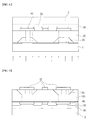
- FIGS. 1A and 1B illustrate the structure of a GaN-based diodeaccording to an embodiment of the present invention.
- the illustrated GaN-based diode includes an intrinsic GaN-based semiconductor layer 30, n+type GaN-based semiconductor layers 50 configured to have a first conductivity type and bonded to the intrinsic GaN-based semiconductor layer 30, a first electrode 7 made of metal and placed on a surface opposite a surface bonded to the intrinsic GaN-based semiconductor layer 30, a second electrode 60 placed on a surface opposite to the Schottky junctions of the n+type GaN-based semiconductor layers 50of the first conductivity type, and p type voltage-resistant layers 20 formed in some regions of the intrinsic GaN-based semiconductor layer 30 that come in contact with the edges of the first electrode 7.
- the first electrode 7 functions as a kind of Schottky metal.
- the first electrode 7 and the n+type GaN-based semiconductor layer 50 form a Schottky barrier with the intrinsic GaN-based semiconductor layer 30 interposed therebetween. That is, the intrinsic GaN-based semiconductor layer 30 may function as an epitaxial layer in which a depletion layer between the first electrode 7, that is, Schottky metal, and the n+type GaN-based semiconductor layer 50 is formed.
- the n+type GaN-based semiconductor layer 50 transfers its electrons to the intrinsic GaN-based semiconductor layer 30 so that the intrinsic GaN-based semiconductor layer 30 functions as an epitaxial layer in terms of the Schottky barrier structure.
- an n-type GaN-based semiconductor layer doped with impurities having a lower concentration than those of the n+type GaN-based semiconductor layer 50 may be formed instead of the intrinsic GaN-based semiconductor layer 30.
- the illustrated GaN-based diode includes Threading Dislocation (TD) blocking insulating layers 10 and 40 for blocking a TD in the central area of the stack structure and areas overlapped with the p type voltage-resistant layers 20.
- the TD blocking insulating layers 10 and 40 may include lower TD blocking insulating layers 40 formed on the junctions of the intrinsic GaN-based semiconductor layer 30 and the n+type GaN-based semiconductor layer 50 and upper TD blocking insulating layers 10 formed on the junctions of the intrinsic GaN-based semiconductor layer 30 and the first electrode 7.
- the TD blocking insulating layers 10 and 40 function to suppress a side effect attributable to a TD that is generated when fabricating the GaN-based Schottky diodeaccording to the present embodiment using a method of growing a GaN-based semiconductor on a sapphire substrate having a relatively low manufacturing cost in an Epitaxial Lateral Overgrowth (ELO) manner.
- ELO Epitaxial Lateral Overgrowth
- a TD may be formed in the central area of the stack structure. As illustrated, the upper/lower TD blocking insulating layers 10 and 40 are formed in order to block such a TD.
- the p type voltage-resistant layers 20 are also formed under the edges of the first electrode 7, that is, areas on which a TD is concentrated, thus contributing to obtaining a high voltage-resistant characteristic along with the TD blocking insulating layers 10 and 40.
- the first electrode 7 functions as the anode electrode of the GaN-based Schottky diode
- the second electrode 60 functions as the cathode electrode of the GaN-based Schottky diode.
- the first electrode 7 is made of metal because it functions as Schottky metalthat forms the Schottky junction.
- the first electrode 7 may be formed by depositing Ni/Au.
- the second electrode 60 may be made of conductive materials. If the usage of the GaN-based Schottky diode and heat-dissipation processing for the GaN-based Schottky diode is important, the second electrode 60may be made of metal materials having excellent thermal conductivity. For example, the second electrode 60 may be formed by depositing Ti/Al/Ti/Au or using AuSn. In some implementations, the second electrode 60 may be attached to a thermal conductive substrate for dissipating heat, or may be part of a structure (e.g., a via hole or a draw line) for configuring a circuit.
- a structure e.g., a via hole or a draw line
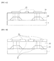
- FIG. 2A is a cross-sectional view of the depletion layer DA when the GaN-based diode of FIG. 1A is in the floating state
- FIG. 2B is a cross-sectional view of the depletion layer DA when the GaN-based diode of FIG. 1A is in the reverse bias state.
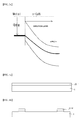
- FIG. 3A is a graph illustratingthe potential barrier of the depletion layer when the GaN-based diode of FIG. 1A is in the floating state
- FIG. 3B is a graph illustratingthe potential barrier of the depletion layer when the GaN-based diode of FIG. 1A is in the forward bias state
- FIG. 3C is a graph illustratingthe potential barrier of the depletion layer when the GaN-based diode of FIG. 1A is in the reverse bias state.
- the potential barrier for blocking a movement of charge carriers between the anode electrode and the cathode electrode in the floating state is formed at the junction of metal and the n type GaN-based semiconductor.
- FIGS. 4A to 4G are cross-sectional views illustrating a method of fabricatingthe GaN-based diode of FIG. 1A .
- a p type GaN-based semiconductor layer 20-1 is formed on a sapphire substrate 1 to a specific thickness.
- the p type GaN-based semiconductor layer 20-1 having a thickness of 2 ⁇ m may be formed using Mg as a dopant.
- an intrinsic GaN-based semiconductor layer may be formed instead of the p type GaN-based semiconductor layer 20-1.
- the p type GaN-based semiconductor layer 20-1 may be formed in such a way as to grow the p type GaN-based semiconductor layer 20-1 on a GaN structurein a ⁇ 11-00> direction.
- the p type GaN-based semiconductor layer 20-1 may be grown on the GaN structurein a ⁇ 112-0> direction.
- a seed p type GaN-based semiconductor layer 20-2 is formed by etching the p type GaN-based semiconductor layer 20-1 of FIG. 4A .
- detained processes such as photolithography for etching, are included. It may be seen that some of the sapphire substrate 1 has been etched by the etching.
- the intrinsic GaN-based semiconductor layer 30 is formed by growing the GaN-based semiconductor using the seed p type GaN-based semiconductor layer 20-2 as a seed layer in an ELO manner.
- the lower TD blocking insulating layers 40 are formed on the intrinsic GaN-based semiconductor layer 30.
- the lower TD blocking insulating layers 40 may be deposited using SiO 2 materials, for example, and may be then formed into shapes, such as those illustrated in FIG. 4C , by an etch process, such as photolithography.
- the seed p type GaN-based semiconductor layers 20-2 are partially grown by the ELO growth, thus having the shapes of the p type voltage-resistant layers 20 of FIG. 1A .
- the lower TD blocking insulating layers 40 may be selectively formed in the upper regions of the seed p type GaN-based semiconductor layers 20-2 in which a TD is likely to occur and the central area of the entire ELO growth structure.
- the n+type GaN-based semiconductor layers 50 are formed by growing an n+type GaN-based semiconductor in an ELO manner using the lower TD blocking insulating layers 40 as an ELO growth mask.
- the second electrode 60 made of conductive materials is formed on the n+type GaN-based semiconductor layers 50 and the lower TD blocking insulating layers 40.
- a second substrate 2 made of metal is attached to the second electrode 60.
- the second electrode 60 may be formed of a conductive layermade of non-metallic conductive materials, but is advantageously made of metal, such as Ti/Al/Au or Ni/Au, or AuSn because the usage of the Schottky diode and the dissipation of heat in terms of its characteristics are important.
- the second substrate 2 may be made of non-metal capable of securing physical strength, but is advantageously made of metal, such as Mo/Si in terms of the dissipation of heat.
- the stack structure of FIG. 4E may be turned inside out, and a process of removing the sapphire substrate 1 may be performed.
- the sapphire substrate 1 may be removed by a laser lift-off process.
- dry etch may be performed in order to remove a surface damaged by the lift-off process.
- the upper TD blocking insulating layers 10 are formed at places overlapped with the lower TD blocking insulating layers 40 over a surface from which the sapphire substrate 1 has been removed.
- the upper TD blocking insulating layers 10 may be deposited using SiO 2 materials, for example, and may be then formed into shapes, such as those illustrated in FIG. 4F , by an etch process, such as photolithography.
- the first electrode 7 may be formed by depositing Ni/Au.
- the first electrode 7 is formed in such a way as to cover part (e.g., about a half) of the upper region of the p type voltage-resistant layer 20 so that the p type voltage-resistant layers 20 are placed under the edges of the first electrode 7.
- GaN-based diode according to an embodiment of the present invention is implemented, there is an advantage in that a Schottky diode having excellent characteristics can be cheaply fabricated.
- the present invention is advantageous in that it can provide a Schottky diode that is fabricated in a sapphire substrate and that has a high voltage-resistant characteristic.
Landscapes
- Electrodes Of Semiconductors (AREA)
- Chemical & Material Sciences (AREA)
- Crystallography & Structural Chemistry (AREA)
Applications Claiming Priority (1)
| Application Number | Priority Date | Filing Date | Title |
|---|---|---|---|
| KR1020130090052A KR20150014641A (ko) | 2013-07-30 | 2013-07-30 | 질화갈륨계 다이오드 및 그 제조 방법 |
Publications (2)
| Publication Number | Publication Date |
|---|---|
| EP2833412A2 true EP2833412A2 (de) | 2015-02-04 |
| EP2833412A3 EP2833412A3 (de) | 2015-03-04 |
Family
ID=51225381
Family Applications (1)
| Application Number | Title | Priority Date | Filing Date |
|---|---|---|---|
| EP14179127.7A Withdrawn EP2833412A3 (de) | 2013-07-30 | 2014-07-30 | Galliumnitridbasierte Schottky-Diode und Verfahren zur Herstellung davon |
Country Status (5)
| Country | Link |
|---|---|
| US (1) | US9142688B2 (de) |
| EP (1) | EP2833412A3 (de) |
| JP (1) | JP2015029099A (de) |
| KR (1) | KR20150014641A (de) |
| CN (1) | CN104347733A (de) |
Families Citing this family (3)
| Publication number | Priority date | Publication date | Assignee | Title |
|---|---|---|---|---|
| JP6549552B2 (ja) * | 2016-12-27 | 2019-07-24 | トヨタ自動車株式会社 | スイッチング素子の製造方法 |
| JP6616280B2 (ja) | 2016-12-27 | 2019-12-04 | トヨタ自動車株式会社 | スイッチング素子 |
| CN113921593B (zh) * | 2021-10-08 | 2025-06-17 | 泰科天润半导体科技(北京)有限公司 | 一种耐高压SiC PIN二极管及其制造方法 |
Citations (1)
| Publication number | Priority date | Publication date | Assignee | Title |
|---|---|---|---|---|
| KR970077615A (ko) | 1996-05-13 | 1997-12-12 | 월리엄 이. 갈라스 | 고주파 특성을 가진 GaAs 기판위에 쇼트키 장벽 다이오드를 만드는 방법 |
Family Cites Families (22)
| Publication number | Priority date | Publication date | Assignee | Title |
|---|---|---|---|---|
| JPH11130597A (ja) * | 1997-10-24 | 1999-05-18 | Mitsubishi Cable Ind Ltd | 転位線の伝搬方向の制御方法およびその用途 |
| JP5130641B2 (ja) * | 2006-03-31 | 2013-01-30 | サンケン電気株式会社 | 複合半導体装置 |
| TWI240969B (en) * | 2003-06-06 | 2005-10-01 | Sanken Electric Co Ltd | Nitride semiconductor device and method for manufacturing same |
| TWI243399B (en) * | 2003-09-24 | 2005-11-11 | Sanken Electric Co Ltd | Nitride semiconductor device |
| US7084475B2 (en) * | 2004-02-17 | 2006-08-01 | Velox Semiconductor Corporation | Lateral conduction Schottky diode with plural mesas |
| WO2008062734A1 (en) * | 2006-11-20 | 2008-05-29 | Panasonic Corporation | Nonvolatile storage element, nonvolatile storage element array and its fabrication process |
| JP4961969B2 (ja) * | 2006-11-22 | 2012-06-27 | 住友電気工業株式会社 | ショットキバリアダイオードおよびショットキ接合を有する半導体デバイスを作製する方法 |
| US8232558B2 (en) * | 2008-05-21 | 2012-07-31 | Cree, Inc. | Junction barrier Schottky diodes with current surge capability |
| JP5056658B2 (ja) * | 2008-08-04 | 2012-10-24 | 住友電気工業株式会社 | ガードリング構造,その形成方法および半導体デバイス |
| JP2010272577A (ja) * | 2009-05-19 | 2010-12-02 | Takehisa Sasaki | 放射線検出素子、及び、放射線検出装置 |
| JP4638958B1 (ja) * | 2009-08-20 | 2011-02-23 | 株式会社パウデック | 半導体素子の製造方法 |
| WO2011145309A1 (ja) * | 2010-05-18 | 2011-11-24 | パナソニック株式会社 | 半導体チップおよびその製造方法 |
| JP5457292B2 (ja) * | 2010-07-12 | 2014-04-02 | パナソニック株式会社 | 窒化物半導体装置 |
| JP5306392B2 (ja) * | 2011-03-03 | 2013-10-02 | 株式会社東芝 | 半導体整流装置 |
| US9093395B2 (en) * | 2011-09-02 | 2015-07-28 | Avogy, Inc. | Method and system for local control of defect density in gallium nitride based electronics |
| US8778788B2 (en) * | 2011-10-11 | 2014-07-15 | Avogy, Inc. | Method of fabricating a gallium nitride merged P-i-N Schottky (MPS) diode |
| US20120056743A1 (en) | 2011-11-11 | 2012-03-08 | Kent David Lyon | Hvac air filter check reminder refrigerator magnet |
| KR101256467B1 (ko) * | 2012-02-06 | 2013-04-19 | 삼성전자주식회사 | 질화물계 이종접합 반도체 소자 및 그 제조 방법 |
| US8981528B2 (en) * | 2012-11-16 | 2015-03-17 | Vishay General Semiconductor Llc | GaN-based Schottky diode having partially recessed anode |
| EP2747143A1 (de) * | 2012-12-19 | 2014-06-25 | Nxp B.V. | GaN-HEMTs und GaN-Dioden |
| US8975640B2 (en) * | 2013-04-29 | 2015-03-10 | Infineon Techonologies Austria AG | Heterojunction semiconductor device and manufacturing method |
| EP3116028B1 (de) * | 2013-06-24 | 2021-03-24 | Ideal Power Inc. | Systeme, schaltungen, vorrichtungen und verfahren mit bidirektionalen bipolartransistoren |
-
2013
- 2013-07-30 KR KR1020130090052A patent/KR20150014641A/ko not_active Ceased
-
2014
- 2014-07-30 CN CN201410369784.5A patent/CN104347733A/zh active Pending
- 2014-07-30 JP JP2014154373A patent/JP2015029099A/ja not_active Withdrawn
- 2014-07-30 EP EP14179127.7A patent/EP2833412A3/de not_active Withdrawn
- 2014-07-30 US US14/447,225 patent/US9142688B2/en not_active Expired - Fee Related
Patent Citations (1)
| Publication number | Priority date | Publication date | Assignee | Title |
|---|---|---|---|---|
| KR970077615A (ko) | 1996-05-13 | 1997-12-12 | 월리엄 이. 갈라스 | 고주파 특성을 가진 GaAs 기판위에 쇼트키 장벽 다이오드를 만드는 방법 |
Also Published As
| Publication number | Publication date |
|---|---|
| US9142688B2 (en) | 2015-09-22 |
| EP2833412A3 (de) | 2015-03-04 |
| KR20150014641A (ko) | 2015-02-09 |
| US20150034964A1 (en) | 2015-02-05 |
| JP2015029099A (ja) | 2015-02-12 |
| CN104347733A (zh) | 2015-02-11 |
Similar Documents
| Publication | Publication Date | Title |
|---|---|---|
| US11342420B2 (en) | Heterojunction devices and methods for fabricating the same | |
| US8933532B2 (en) | Schottky diode with buried layer in GaN materials | |
| US8841741B2 (en) | High breakdown voltage semiconductor rectifier | |
| US20150270356A1 (en) | Vertical nitride semiconductor device | |
| US9922838B2 (en) | Selective, electrochemical etching of a semiconductor | |
| US8981432B2 (en) | Method and system for gallium nitride electronic devices using engineered substrates | |
| US9502544B2 (en) | Method and system for planar regrowth in GaN electronic devices | |
| CN105144392B (zh) | 利用再生长氮化镓层制造混合的pn结与肖特基二极管的方法 | |
| US8823148B2 (en) | Diode with epitaxially grown semiconductor layers | |
| US8304783B2 (en) | Schottky diodes including polysilicon having low barrier heights and methods of fabricating the same | |
| US9397186B2 (en) | Method of fabricating a gallium nitride merged P-I-N schottky (MPS) diode by regrowth and etch back | |
| KR20150087335A (ko) | 쇼트키 다이오드들 및 그것을 제조하는 방법 | |
| US20130164893A1 (en) | Fabrication of floating guard rings using selective regrowth | |
| US9142688B2 (en) | Gallium nitride-based diode and method of fabricating the same | |
| JP2019102552A (ja) | ダイオード素子およびダイオード素子の製造方法 | |
| Park et al. | 1kV AlGaN/GaN power SBDs with reduced on resistances | |
| US9466552B2 (en) | Vertical semiconductor device having a non-conductive substrate and a gallium nitride layer | |
| US20130299840A1 (en) | Schottky barrier diode and manufacturing method thereof | |
| US11271117B2 (en) | Stacked high-blocking III-V power semiconductor diode | |
| JP2015046482A (ja) | 半導体装置およびモジュール |
Legal Events
| Date | Code | Title | Description |
|---|---|---|---|
| PUAL | Search report despatched |
Free format text: ORIGINAL CODE: 0009013 |
|
| 17P | Request for examination filed |
Effective date: 20140818 |
|
| AK | Designated contracting states |
Kind code of ref document: A2 Designated state(s): AL AT BE BG CH CY CZ DE DK EE ES FI FR GB GR HR HU IE IS IT LI LT LU LV MC MK MT NL NO PL PT RO RS SE SI SK SM TR |
|
| AX | Request for extension of the european patent |
Extension state: BA ME |
|
| PUAI | Public reference made under article 153(3) epc to a published international application that has entered the european phase |
Free format text: ORIGINAL CODE: 0009012 |
|
| AK | Designated contracting states |
Kind code of ref document: A3 Designated state(s): AL AT BE BG CH CY CZ DE DK EE ES FI FR GB GR HR HU IE IS IT LI LT LU LV MC MK MT NL NO PL PT RO RS SE SI SK SM TR |
|
| AX | Request for extension of the european patent |
Extension state: BA ME |
|
| RIC1 | Information provided on ipc code assigned before grant |
Ipc: H01L 29/872 20060101ALI20150129BHEP Ipc: H01L 29/06 20060101ALN20150129BHEP Ipc: H01L 29/20 20060101ALI20150129BHEP Ipc: H01L 21/329 20060101AFI20150129BHEP Ipc: H01L 29/32 20060101ALN20150129BHEP |
|
| STAA | Information on the status of an ep patent application or granted ep patent |
Free format text: STATUS: THE APPLICATION IS DEEMED TO BE WITHDRAWN |
|
| 18D | Application deemed to be withdrawn |
Effective date: 20180201 |