EP2747143A1 - GaN-HEMTs und GaN-Dioden - Google Patents
GaN-HEMTs und GaN-Dioden Download PDFInfo
- Publication number
- EP2747143A1 EP2747143A1 EP12198130.2A EP12198130A EP2747143A1 EP 2747143 A1 EP2747143 A1 EP 2747143A1 EP 12198130 A EP12198130 A EP 12198130A EP 2747143 A1 EP2747143 A1 EP 2747143A1
- Authority
- EP
- European Patent Office
- Prior art keywords
- layer
- dielectric layer
- dielectric
- gate
- over
- Prior art date
- Legal status (The legal status is an assumption and is not a legal conclusion. Google has not performed a legal analysis and makes no representation as to the accuracy of the status listed.)
- Withdrawn
Links
- 238000004518 low pressure chemical vapour deposition Methods 0.000 claims description 26
- 238000000623 plasma-assisted chemical vapour deposition Methods 0.000 claims description 24
- 238000000034 method Methods 0.000 claims description 23
- 239000004065 semiconductor Substances 0.000 claims description 16
- 229910002704 AlGaN Inorganic materials 0.000 claims description 14
- 239000000758 substrate Substances 0.000 claims description 12
- 238000004519 manufacturing process Methods 0.000 claims description 5
- 150000004767 nitrides Chemical class 0.000 description 38
- 229910002601 GaN Inorganic materials 0.000 description 27
- 229910052751 metal Inorganic materials 0.000 description 14
- 239000002184 metal Substances 0.000 description 14
- 239000000463 material Substances 0.000 description 11
- 230000008569 process Effects 0.000 description 11
- 238000013461 design Methods 0.000 description 10
- 238000000151 deposition Methods 0.000 description 8
- 230000008021 deposition Effects 0.000 description 8
- 230000005684 electric field Effects 0.000 description 7
- 238000000059 patterning Methods 0.000 description 7
- 230000015556 catabolic process Effects 0.000 description 5
- 238000001465 metallisation Methods 0.000 description 5
- 238000002161 passivation Methods 0.000 description 5
- 229910052581 Si3N4 Inorganic materials 0.000 description 4
- 230000004888 barrier function Effects 0.000 description 4
- 239000003989 dielectric material Substances 0.000 description 4
- 230000036039 immunity Effects 0.000 description 4
- HQVNEWCFYHHQES-UHFFFAOYSA-N silicon nitride Chemical compound N12[Si]34N5[Si]62N3[Si]51N64 HQVNEWCFYHHQES-UHFFFAOYSA-N 0.000 description 4
- JMASRVWKEDWRBT-UHFFFAOYSA-N Gallium nitride Chemical compound [Ga]#N JMASRVWKEDWRBT-UHFFFAOYSA-N 0.000 description 3
- XUIMIQQOPSSXEZ-UHFFFAOYSA-N Silicon Chemical compound [Si] XUIMIQQOPSSXEZ-UHFFFAOYSA-N 0.000 description 3
- 238000000137 annealing Methods 0.000 description 3
- 230000008859 change Effects 0.000 description 3
- 238000010276 construction Methods 0.000 description 3
- 230000000694 effects Effects 0.000 description 3
- 229910052710 silicon Inorganic materials 0.000 description 3
- 239000010703 silicon Substances 0.000 description 3
- HBMJWWWQQXIZIP-UHFFFAOYSA-N silicon carbide Chemical compound [Si+]#[C-] HBMJWWWQQXIZIP-UHFFFAOYSA-N 0.000 description 3
- 230000005533 two-dimensional electron gas Effects 0.000 description 3
- PXHVJJICTQNCMI-UHFFFAOYSA-N Nickel Chemical compound [Ni] PXHVJJICTQNCMI-UHFFFAOYSA-N 0.000 description 2
- 238000013459 approach Methods 0.000 description 2
- 230000007423 decrease Effects 0.000 description 2
- 238000009826 distribution Methods 0.000 description 2
- 239000002019 doping agent Substances 0.000 description 2
- 238000005530 etching Methods 0.000 description 2
- 239000012535 impurity Substances 0.000 description 2
- 239000012212 insulator Substances 0.000 description 2
- 238000001459 lithography Methods 0.000 description 2
- 230000004048 modification Effects 0.000 description 2
- 238000012986 modification Methods 0.000 description 2
- 230000007935 neutral effect Effects 0.000 description 2
- 238000010943 off-gassing Methods 0.000 description 2
- 238000009832 plasma treatment Methods 0.000 description 2
- 230000010287 polarization Effects 0.000 description 2
- 229910010271 silicon carbide Inorganic materials 0.000 description 2
- 238000001039 wet etching Methods 0.000 description 2
- UFHFLCQGNIYNRP-UHFFFAOYSA-N Hydrogen Chemical compound [H][H] UFHFLCQGNIYNRP-UHFFFAOYSA-N 0.000 description 1
- 229910052782 aluminium Inorganic materials 0.000 description 1
- 239000004411 aluminium Substances 0.000 description 1
- XAGFODPZIPBFFR-UHFFFAOYSA-N aluminium Chemical compound [Al] XAGFODPZIPBFFR-UHFFFAOYSA-N 0.000 description 1
- RNQKDQAVIXDKAG-UHFFFAOYSA-N aluminum gallium Chemical compound [Al].[Ga] RNQKDQAVIXDKAG-UHFFFAOYSA-N 0.000 description 1
- 230000009286 beneficial effect Effects 0.000 description 1
- 230000008901 benefit Effects 0.000 description 1
- 238000005229 chemical vapour deposition Methods 0.000 description 1
- 238000002109 crystal growth method Methods 0.000 description 1
- 238000006731 degradation reaction Methods 0.000 description 1
- 230000001419 dependent effect Effects 0.000 description 1
- 238000001312 dry etching Methods 0.000 description 1
- -1 e.g. Substances 0.000 description 1
- 230000005669 field effect Effects 0.000 description 1
- 239000007789 gas Substances 0.000 description 1
- 239000001257 hydrogen Substances 0.000 description 1
- 229910052739 hydrogen Inorganic materials 0.000 description 1
- 238000002347 injection Methods 0.000 description 1
- 239000007924 injection Substances 0.000 description 1
- 238000001451 molecular beam epitaxy Methods 0.000 description 1
- 229910052759 nickel Inorganic materials 0.000 description 1
- 238000000206 photolithography Methods 0.000 description 1
- 238000005036 potential barrier Methods 0.000 description 1
- 238000012545 processing Methods 0.000 description 1
- 230000009467 reduction Effects 0.000 description 1
- 229910052594 sapphire Inorganic materials 0.000 description 1
- 239000010980 sapphire Substances 0.000 description 1
- 239000000243 solution Substances 0.000 description 1
- 230000002269 spontaneous effect Effects 0.000 description 1
Images


Classifications
-
- H—ELECTRICITY
- H01—ELECTRIC ELEMENTS
- H01L—SEMICONDUCTOR DEVICES NOT COVERED BY CLASS H10
- H01L29/00—Semiconductor devices specially adapted for rectifying, amplifying, oscillating or switching and having potential barriers; Capacitors or resistors having potential barriers, e.g. a PN-junction depletion layer or carrier concentration layer; Details of semiconductor bodies or of electrodes thereof ; Multistep manufacturing processes therefor
- H01L29/40—Electrodes ; Multistep manufacturing processes therefor
- H01L29/41—Electrodes ; Multistep manufacturing processes therefor characterised by their shape, relative sizes or dispositions
- H01L29/423—Electrodes ; Multistep manufacturing processes therefor characterised by their shape, relative sizes or dispositions not carrying the current to be rectified, amplified or switched
- H01L29/42312—Gate electrodes for field effect devices
- H01L29/42316—Gate electrodes for field effect devices for field-effect transistors
-
- H—ELECTRICITY
- H01—ELECTRIC ELEMENTS
- H01L—SEMICONDUCTOR DEVICES NOT COVERED BY CLASS H10
- H01L29/00—Semiconductor devices specially adapted for rectifying, amplifying, oscillating or switching and having potential barriers; Capacitors or resistors having potential barriers, e.g. a PN-junction depletion layer or carrier concentration layer; Details of semiconductor bodies or of electrodes thereof ; Multistep manufacturing processes therefor
- H01L29/40—Electrodes ; Multistep manufacturing processes therefor
- H01L29/43—Electrodes ; Multistep manufacturing processes therefor characterised by the materials of which they are formed
- H01L29/47—Schottky barrier electrodes
- H01L29/475—Schottky barrier electrodes on AIII-BV compounds
-
- H—ELECTRICITY
- H01—ELECTRIC ELEMENTS
- H01L—SEMICONDUCTOR DEVICES NOT COVERED BY CLASS H10
- H01L23/00—Details of semiconductor or other solid state devices
- H01L23/28—Encapsulations, e.g. encapsulating layers, coatings, e.g. for protection
- H01L23/31—Encapsulations, e.g. encapsulating layers, coatings, e.g. for protection characterised by the arrangement or shape
- H01L23/3157—Partial encapsulation or coating
- H01L23/3171—Partial encapsulation or coating the coating being directly applied to the semiconductor body, e.g. passivation layer
-
- H—ELECTRICITY
- H01—ELECTRIC ELEMENTS
- H01L—SEMICONDUCTOR DEVICES NOT COVERED BY CLASS H10
- H01L29/00—Semiconductor devices specially adapted for rectifying, amplifying, oscillating or switching and having potential barriers; Capacitors or resistors having potential barriers, e.g. a PN-junction depletion layer or carrier concentration layer; Details of semiconductor bodies or of electrodes thereof ; Multistep manufacturing processes therefor
- H01L29/40—Electrodes ; Multistep manufacturing processes therefor
- H01L29/401—Multistep manufacturing processes
- H01L29/4011—Multistep manufacturing processes for data storage electrodes
- H01L29/40114—Multistep manufacturing processes for data storage electrodes the electrodes comprising a conductor-insulator-conductor-insulator-semiconductor structure
-
- H—ELECTRICITY
- H01—ELECTRIC ELEMENTS
- H01L—SEMICONDUCTOR DEVICES NOT COVERED BY CLASS H10
- H01L29/00—Semiconductor devices specially adapted for rectifying, amplifying, oscillating or switching and having potential barriers; Capacitors or resistors having potential barriers, e.g. a PN-junction depletion layer or carrier concentration layer; Details of semiconductor bodies or of electrodes thereof ; Multistep manufacturing processes therefor
- H01L29/66—Types of semiconductor device ; Multistep manufacturing processes therefor
- H01L29/68—Types of semiconductor device ; Multistep manufacturing processes therefor controllable by only the electric current supplied, or only the electric potential applied, to an electrode which does not carry the current to be rectified, amplified or switched
- H01L29/76—Unipolar devices, e.g. field effect transistors
- H01L29/772—Field effect transistors
- H01L29/778—Field effect transistors with two-dimensional charge carrier gas channel, e.g. HEMT ; with two-dimensional charge-carrier layer formed at a heterojunction interface
- H01L29/7786—Field effect transistors with two-dimensional charge carrier gas channel, e.g. HEMT ; with two-dimensional charge-carrier layer formed at a heterojunction interface with direct single heterostructure, i.e. with wide bandgap layer formed on top of active layer, e.g. direct single heterostructure MIS-like HEMT
-
- H—ELECTRICITY
- H01—ELECTRIC ELEMENTS
- H01L—SEMICONDUCTOR DEVICES NOT COVERED BY CLASS H10
- H01L29/00—Semiconductor devices specially adapted for rectifying, amplifying, oscillating or switching and having potential barriers; Capacitors or resistors having potential barriers, e.g. a PN-junction depletion layer or carrier concentration layer; Details of semiconductor bodies or of electrodes thereof ; Multistep manufacturing processes therefor
- H01L29/66—Types of semiconductor device ; Multistep manufacturing processes therefor
- H01L29/86—Types of semiconductor device ; Multistep manufacturing processes therefor controllable only by variation of the electric current supplied, or only the electric potential applied, to one or more of the electrodes carrying the current to be rectified, amplified, oscillated or switched
- H01L29/861—Diodes
- H01L29/872—Schottky diodes
-
- H—ELECTRICITY
- H01—ELECTRIC ELEMENTS
- H01L—SEMICONDUCTOR DEVICES NOT COVERED BY CLASS H10
- H01L23/00—Details of semiconductor or other solid state devices
- H01L23/28—Encapsulations, e.g. encapsulating layers, coatings, e.g. for protection
- H01L23/31—Encapsulations, e.g. encapsulating layers, coatings, e.g. for protection characterised by the arrangement or shape
- H01L23/3157—Partial encapsulation or coating
- H01L23/3192—Multilayer coating
-
- H—ELECTRICITY
- H01—ELECTRIC ELEMENTS
- H01L—SEMICONDUCTOR DEVICES NOT COVERED BY CLASS H10
- H01L29/00—Semiconductor devices specially adapted for rectifying, amplifying, oscillating or switching and having potential barriers; Capacitors or resistors having potential barriers, e.g. a PN-junction depletion layer or carrier concentration layer; Details of semiconductor bodies or of electrodes thereof ; Multistep manufacturing processes therefor
- H01L29/02—Semiconductor bodies ; Multistep manufacturing processes therefor
- H01L29/12—Semiconductor bodies ; Multistep manufacturing processes therefor characterised by the materials of which they are formed
- H01L29/20—Semiconductor bodies ; Multistep manufacturing processes therefor characterised by the materials of which they are formed including, apart from doping materials or other impurities, only AIIIBV compounds
- H01L29/2003—Nitride compounds
-
- H—ELECTRICITY
- H01—ELECTRIC ELEMENTS
- H01L—SEMICONDUCTOR DEVICES NOT COVERED BY CLASS H10
- H01L2924/00—Indexing scheme for arrangements or methods for connecting or disconnecting semiconductor or solid-state bodies as covered by H01L24/00
- H01L2924/0001—Technical content checked by a classifier
- H01L2924/0002—Not covered by any one of groups H01L24/00, H01L24/00 and H01L2224/00
Definitions
- This invention relates to GaN devices, such as high electron mobility transistors (HEMTs) and diodes, and relates to the problem of gate leakage in these devices.
- HEMTs high electron mobility transistors
- diodes diodes
- HEMTs GaN high-mobility transistors
- HV High Voltage
- 2DEG high-density two-dimensional electron gas
- RF radio-frequency
- the basic structure of a HEMT is shown in Figure 1 .
- the current flows between drain (D) and source (S) via the so-called two-dimensional electron gas (2DEG) that is formed at the interface between an AlGaN barrier layer and a top GaN layer (or a capping layer if one is present- not shown in Figure 1 ).
- 2DEG two-dimensional electron gas
- This heterojunction structure incorporates a junction between two materials with different band gaps as the channel instead of a doped region.
- the net result of such a heterojunction is to create a very thin layer of highly mobile conducting electrons with very high concentration or density, giving the channel very low resistivity.
- This layer is known as the two-dimensional electron gas (2DEG).
- 2DEG two-dimensional electron gas
- FET field-effect transistor
- HEMT high-electron mobility transistor
- AlGaN/GaN HEMTs can be fabricated by growing crystalline films of GaN, AlGaN, etc. on a substrate, e.g., sapphire, silicon (Si)(111), silicon carbide (SiC) and so on, through an epitaxial crystal growth method, e.g., metal organic chemical vapor deposition (MOCVD), molecular beam epitaxy (MBE) and so on, and processing the epitaxial substrate thus grown, to form the desired structures.
- MOCVD metal organic chemical vapor deposition
- MBE molecular beam epitaxy
- the semiconductor device is switched between the off-state, in which the 2DEG is disrupted under the Schottky gate, and an on-state in which a high current is produced at a low voltage.
- the design of such devices typically targets a trade-off between power losses in the on-state, off-state and during switching.
- Switching-off is achieved by applying a suitable voltage on the Schottky metal (G) such that the 2DEG under the metal disappears.
- G Schottky metal
- a GaN Schottky diode can be simply thought of as a HEMT without a source contact. In a Schottky diode the current flows between gate and drain. The design of these devices is such that an optimum trade-off is found between the power losses in on-state, off-state and during switching.
- FIG. 2 shows the gate area of the device of Figure 1 in more detail.
- a silicon substrate 10 comprises a GaN buffer layer 10' on which an epitaxially grown GaN layer 12 and an AlGaN barrier layer 14 are formed.
- the GaN layer 12 and the AlGaN barrier layer 14 define a heterojunction, at the interface of which a 2DEG 12' may form.
- a GaN capping layer 16 (which is optional and is not shown in Figure 1 ) separates a first (Si 3 N 4 ) dielectric layer 18 and a Schottky gate 20 from the heterojunction.
- the semiconductor device typically will comprise at least one other (ohmic) electrode, to form a Schottky diode in case of a two-terminal device or two other electrodes in the case of a three-terminal HEMT device, but these electrodes are omitted from Figure 2 for the sake of clarity only.
- the semiconductor device typically has an on-state, in which the 2DEG 12' laterally extends over the full width of the device, e.g. between the source and drain of a HEMT, and an off-state, in which a (negative) bias or gate voltage is applied to the Schottky gate to disrupt the 2DEG 12' underneath the Schottky gate 20.
- an on-state in which the 2DEG 12' laterally extends over the full width of the device, e.g. between the source and drain of a HEMT
- an off-state in which a (negative) bias or gate voltage is applied to the Schottky gate to disrupt the 2DEG 12' underneath the Schottky gate 20.
- the 2DEG 12' extends over the full width of the device in the absence of a gate bias. In a normally-off device, the 2DEG 12' is absent underneath the Schottky gate 20 in the absence of a gate bias.
- One of the problems with such devices is a high leakage current during the off-state.
- Such a leakage current is determined by the potential barrier for electrons between the Schottky metal and the 2DEG.
- a high off-state leakage current is caused by tunnelling through the Schottky/AlGaN barrier near the gate edge.
- the on-state resistance is significantly higher under dynamic conditions (e.g. switching, pulsed, RF) than under DC conditions. This on-state resistance may also change during the lifetime of the device and may therefore cause reliability issues.
- the passivation layer(s) on top of the semiconductor surface has a strong influence on the leakage current and the on-state resistance, and in particular their behaviour on short (switching, RF) and long (degradation) time scales.
- the invention provides a GaN hetereojunction semiconductor device comprising:
- overlap is meant that one layer is over the other, but also extending beyond (i.e. overhanging) the lower layer at least over one edge.
- This structure has three dielectric layers. The lowermost and middle portions of the gate electrode together define the gate foot, and this is associated with two dielectric layers. A thinner first dielectric layer is adjacent the gate edge at the bottom of the gate electrode, and it fills the area where the middle portion overlaps/overhangs the lowermost portion.
- the second dielectric layer corresponds to the layer in the conventional structure, and it is coplanar (i.e. level) with the main middle portion of the gate foot.
- the additional (first) dielectric layer improves the leakage current performance and reduces the on-state resistance of the device.
- the first dielectric layer is preferably over the second dielectric layer (i.e. the second layer is deposited first), and the second dielectric layer has a well in the region of the gate and in which the first dielectric layer is formed.
- the first dielectric layer portion extends to the bottom of the dielectric layer structure in the region of the gate, and it is the only one of the first, second and third dielectric layers beneath the middle gate portion, i.e. the overlap/overhang of the gate middle portion over the gate lowermost portion.
- the first dielectric layer can comprise an LPCVD layer
- the second and third dielectric layers can comprise PECVD layers. All three dielectric layers can for example comprise SiN.
- the length of the overlap of the middle portion over the lowermost portion is in the range 10nm to 100nm.
- the overlap is greater than the twice the thickness of the first dielectric layer, which is for example is in the range 5 to 50nm.
- the overlap is more preferably more than three times the thickness.
- the invention provides a method of manufacturing a semiconductor device comprising:
- Forming the dielectric layer structure can comprise:
- the invention provides a GaN HEMT structure with a three-layer dielectric structure.
- the lowermost and middle portions of the gate electrode together define the gate foot, and this is associated with two dielectric layers.
- a thinner first dielectric layer is adjacent the gate edge at the bottom of the gate electrode.
- the second dielectric layer corresponds to the layer in the conventional structure, and it is level with the main portion of the gate foot.
- Figure 3(a) shows in simplified form the GaN/AlGaN high-mobility transistor (HEMT) structure and Figure 3(b) shows a GaN/AlGaN Schottky diode structure.
- the gate head region 30 labelled in Figure 3(a) corresponds to the gate edge region shown in Figure 2 , although Figure 2 does not show the top head part of the gate structure.
- a metal insulator semiconductor HEMT (“MISHEMT”) is shown in Figure 3(c) .
- N d,neutral CxV FL /q, where C is the capacitance between the metal and the 2DEG per unit area.
- C the capacitance between the metal and the 2DEG per unit area.
- V FL and V TH depend not only on the thickness of the dielectric but also on the charges present in the dielectric or at its interface with the semiconductor.
- Figure 5 shows the relation between the MISHEMT curve ( Figure 4 ) and the leakage current.
- V CA > V TH the 2DEG under the gate head is gone and the electric field near the gate edge is constant and, therefore, the leakage current is constant.
- Figure 6 shows what happens to the value of Rdrift when a certain amount of negative charge ⁇ Q is added in the dielectric or at its interface with the semiconductor.
- Figures 6(a) and 6(b) show the I DS -V GS curves for two different (hypothetical) passivation layer designs. The two designs differ only in the amount of charge in the nitride (either the surface donor concentration or the concentration of fixed charge).
- the I DS -V GS curve shifts to the right (as shown by dashed curves).
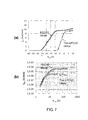
- Figure 7(a) shows the measured I DS -V GS curves of a MISHEMT with 100 nm PECVD nitride and 50 nm LPCVD nitride
- Figure 7(b) shows the drain-gate leakage current as a function of the drain-gate voltage.
- the leakage current remains constant once the reverse bias exceeds the threshold voltage of the MISHEMT and, consequently, the leakage current is lowest for the 50 nm LPCVD nitride.
- the PECVD nitride has a value of V FL well below zero, indicating that not all surface donors are ionized, while the LPCVD nitride has a V FL around zero, so all donors are ionized at zero bias. So, the lower V TH of LPCVD nitride is not only caused by the thinner layer (50nm instead of 100nm) but also by the fact that all surface donors are ionized at zero bias. This can be due to either:
- the invention provides the addition of a thin dielectric layer, with various design options.
- Figure 8(a) shows the known design.
- a lower gate portion 90 (the foot) which is surrounded by the first dielectric layer and an upper gate portion (the head) 92 which is surrounded by the second dielectric layer 94.
- the lower gate portion has a smaller footprint so that there is an edge region to each side of the lower gate portion which is overlapped by the upper gate portion.
- the thickness of the first dielectric layer and the shape of the gate edge are optimized, e.g. for breakdown.
- Figure 8(b) shows the addition of a thin dielectric 96 near the edge of the lower gate portion.
- the addition of the thin dielectric layer has the effect that the threshold voltage of the MISHEMT structure formed by the gate head the thin dielectric 96 and the semiconductor adjacent to the edge of the gate foot is lowered, and, as described above, the leakage current is lowered.
- the resulting structure has three layers.
- the gate foot has a bottom part 98 surrounded by the additional dielectric 96.
- the top part of the gate foot (which is the middle layer of the three layer gate structure) overlaps the additional dielectric layer 96 by a distance L as shown.
- the gate head is not changed. The electric field distribution in the rest of the dielectric under and adjacent to the gate head is thus not changed.
- the additional dielectric material 96 may or may not be the same as the first dielectric material 18.
- a realistic thickness (shown as "t” in Figure 8(b) ) is for example 15 nm, and more generally in the range 5nm to 50nm.
- this layer L needs only to be a few tens of nanometers, for example 30 nm. Typically, L should be larger than two times the thickness t of the thin dielectric layer.
- the additional dielectric layer 96 can extend well into the drift region and may even cover the full area between gate and drain (and gate and source). This is appropriate with respect to leakage current. However, it is not optimal with respect to immunity of the drift resistance against charge variations on the interfaces or in the nitrides (because V FL is close to zero).
- the additional dielectric material 96 can be limited to the gate edge area, for example extending with a length L tot which is slightly larger than the desired overlap distance L of the top part of the gate foot over the bottom part of the gate foot.
- This value Ltot can equal the minimum value of L (e.g. at least two times the thickness t) plus a safety margin for process tolerances. This is shown in Figure 8(c) .
- the threshold voltage of the dielectric for a given thickness can be further reduced by lowering V FL . This can be done by choosing the right material (e.g. the LPCVD nitride as presented in Figure 7 ) or by modification of the material.
- a cavity 99 air or other gas
- This is obtained by etching away the dielectric, and this can give a low leakage current. This could be realized by wet etching and subsequent deposition of a non-conformal dielectric.
- the material of the dielectric in the remaining drift region i.e. the dielectric layers 18,94. This material should provide a good immunity against charge variations on the interfaces or in the nitrides, i.e. a high V FL .
- the PECVD material discussed with reference to Figure 7 is one suitable choice. Modification of this material is also an option, e.g. by doping or plasma treatment. More specifically, the two materials may be the same after deposition. Only after the gate etch, the dielectric in the drift region is modified (e.g. doping, plasma treatment) in order increase V FL to obtain the immunity against charge variations.
- the thin additional dielectric layer is applied to both the drain and source sides of the gate. It can also be applied to the drain side only.
- the low leakage has been achieved by adding a thin dielectric to the conventional gate edge construction.
- Low leakage can also be obtained by reducing the dielectric layer thickness under the gate of the conventional gate edge construction.
- the disadvantage, however, of this is, as compared to the solution above, that the high electric field peak at the edge of the gate head, together with the thin dielectric there, may cause dielectric breakdown or reliability problems.
- Figure 9(a) shows the conventional dielectric stack
- Figure 9(b) shows a reduced thickness under the gate head, giving rise to possible dielectric breakdown at region 100.
- an additional silicon nitride layer to provide the combination of two different silicon nitride passivation layers, can be implemented using a combination of plasma enhanced chemical vapor deposition (PECVD) and low pressure chemical vapor deposition (LPCVD).
- PECVD plasma enhanced chemical vapor deposition
- LPCVD low pressure chemical vapor deposition
- FIG. 10 A first process is shown in Figure 10 .
- the additional thin dielectric layer is lowest in the region of the gate, it is not deposited as the lowest layer, as in the examples of Figure 8(b) and 8(c) .
- the process starts with the deposition of PECVD nitride 110 over the GaN/AlGaN substrate 112, typically at 400°C. After optional annealing of this nitride and lithography, the actual patterning is performed with a buffered oxide etch to form gate and drain (and source for a three terminal device) openings as shown in Figure 10(a) .
- This wet etch which has proven not to impact the 2DEG sheet resistance, creates sloped contacts to the source/drain and gate areas. Instead of opening the source/drain and the gate, it could also be preferred to open the source/drain areas later in the process.
- the sloped sidewalls however are beneficial for a good step coverage for the respective source/drain and gate metal depositions.
- Figure 10(a) thus shown in cross-section of the GaN substrate wafer after PECVD silicon nitride deposition and patterning in source/drain and gate areas.
- the next step is the deposition of LPCVD nitride 114, typically at 850°C, covering again the gate foot and source/drain contacts as shown in Figure 10(b) .
- LPCVD after PECVD is not a typical order in mainstream manufacturing, since PECVD nitride is considered as a lower quality material and outgassing of hydrogen can occur during the ramp up of the temperature to 850°C.
- this process has been demonstrated to work without any problem.
- Patterning of the source/drain contact areas is performed with a dry etch, removing LPCVD nitride inside the PECVD window. Should only the gate area be opened in the previous step, the etch patterns the LPCVD/PECVD stack in one go.
- Figure 10(b) instead shows LPCVD nitride sidewalls present in the source/drain areas, avoiding the metal of the ohmic layer stack to be directly in contact with a low-quality PECVD nitride (layer 110), which has been found to interact during the annealing step.
- This annealing step typically performed at temperatures around 900°C for one minute, is needed to ensure good ohmic contact to the GaN.
- Ohmic metal deposition is performed, typically starting with a bilayer of Ti/Al, and patterning is performed with a dry etch to form the metal drain (and source) contact 116.
- the etch process consumes part of the LPCVD nitride outside the ohmic contact area as shown in Figure10(b) , and therefore also in the gate foot.
- An additional PECVD nitride deposition immediately after the LPCVD nitride can optionally be used to prevent the variation of LPCVD nitride consumption over the wafer shown in Figure 10(b) .
- the next step is PECVD nitride deposition to cover the ohmic contacts before the gate metal is deposited.
- This cover acts as protection.
- This cover area is shown as 118 in Figure 10(c) .
- Removal of the PECVD nitride outside the ohmic contact areas is performed using wet etching after a photomasking step, using a buffered oxide etch which is very selective to LPCVD nitride.
- the Schottky gate metal can be deposited without protecting the source/drain contacts with the additional silicon nitride layer 118. This has been demonstrated to work.
- the step before gate metal deposition is gate area patterning by dry etching the LPCVD nitride 114 inside the PECVD window, creating the desired extension of the LPCVD nitride 114 in the gate foot.
- the patterned opening is shown as 120 in Figure 10(c) .
- the gate is patterned using photolithography, either dry or wet.
- the process follows a standard back end metallization, typically using typically PECVD nitrides as intermetal dielectrics and thick layers of aluminium.
- Figure 10(c) shows the cross-section after completion of the Schottky gate patterning.
- the PECVD nitride protecting the ohmic metal before gate metal deposition is also optional.
- Figure 11 shows the structure with no nitride cap and without removing the PECVD layer 110 at the location of the drain contact.
- the LPCVD nitride 114 is only present inside the gate, not in the source/drain contacts. Subsequently, etching the drain and source contact holes removes both layers 110 and 114 locally in one step.
- the LPCVD nitride can be deposited first.
- One reason to do this is that it is more straightforward in mainstream silicon fabrication plants.
- LPCVD furnaces are typically used in a variety of different processes, so outgassing of PECVD nitride may be unwanted from a standard production point of view.
- the process steps are more or less copied from the PECVD-first approach and also several different routes can be taken.
- One possible end-result is shown in Figure 12 .
- the PECVD nitride 132 is patterned after the LPCVD nitride patterning, so misalignment tolerances need to be taken into account.
Landscapes
- Engineering & Computer Science (AREA)
- Microelectronics & Electronic Packaging (AREA)
- Power Engineering (AREA)
- Physics & Mathematics (AREA)
- Condensed Matter Physics & Semiconductors (AREA)
- General Physics & Mathematics (AREA)
- Computer Hardware Design (AREA)
- Ceramic Engineering (AREA)
- Manufacturing & Machinery (AREA)
- Junction Field-Effect Transistors (AREA)
Priority Applications (3)
| Application Number | Priority Date | Filing Date | Title |
|---|---|---|---|
| EP12198130.2A EP2747143A1 (de) | 2012-12-19 | 2012-12-19 | GaN-HEMTs und GaN-Dioden |
| US14/108,042 US8962461B2 (en) | 2012-12-19 | 2013-12-16 | GaN HEMTs and GaN diodes |
| CN201310706281.8A CN103887334B (zh) | 2012-12-19 | 2013-12-19 | GaN高电子迁移率晶体管和GaN二极管 |
Applications Claiming Priority (1)
| Application Number | Priority Date | Filing Date | Title |
|---|---|---|---|
| EP12198130.2A EP2747143A1 (de) | 2012-12-19 | 2012-12-19 | GaN-HEMTs und GaN-Dioden |
Publications (1)
| Publication Number | Publication Date |
|---|---|
| EP2747143A1 true EP2747143A1 (de) | 2014-06-25 |
Family
ID=47632717
Family Applications (1)
| Application Number | Title | Priority Date | Filing Date |
|---|---|---|---|
| EP12198130.2A Withdrawn EP2747143A1 (de) | 2012-12-19 | 2012-12-19 | GaN-HEMTs und GaN-Dioden |
Country Status (3)
| Country | Link |
|---|---|
| US (1) | US8962461B2 (de) |
| EP (1) | EP2747143A1 (de) |
| CN (1) | CN103887334B (de) |
Cited By (3)
| Publication number | Priority date | Publication date | Assignee | Title |
|---|---|---|---|---|
| CN108074964A (zh) * | 2016-11-18 | 2018-05-25 | 安世有限公司 | 低电阻低泄漏器件 |
| US10014401B2 (en) | 2016-01-25 | 2018-07-03 | Electronics And Telecommunications Research Institute | Semiconductor device with passivation layer for control of leakage current |
| EP3823036A1 (de) * | 2019-11-18 | 2021-05-19 | Imec VZW | Verfahren zur skalierung einer gate-länge |
Families Citing this family (10)
| Publication number | Priority date | Publication date | Assignee | Title |
|---|---|---|---|---|
| KR20150014641A (ko) * | 2013-07-30 | 2015-02-09 | 서울반도체 주식회사 | 질화갈륨계 다이오드 및 그 제조 방법 |
| TWI577022B (zh) * | 2014-02-27 | 2017-04-01 | 台達電子工業股份有限公司 | 半導體裝置與應用其之半導體裝置封裝體 |
| EP2908344A1 (de) | 2014-02-12 | 2015-08-19 | Nxp B.V. | Halbleitervorrichtung mit Heteroübergang |
| JP2015222912A (ja) * | 2014-05-23 | 2015-12-10 | 三菱電機株式会社 | リニアライザ |
| EP3179515A1 (de) | 2015-12-10 | 2017-06-14 | Nexperia B.V. | Halbleiterbauelement und verfahren zur herstellung eines halbleiterbauelements |
| US10134596B1 (en) * | 2017-11-21 | 2018-11-20 | Texas Instruments Incorporated | Recessed solid state apparatuses |
| CN110047742A (zh) * | 2019-03-08 | 2019-07-23 | 福建省福联集成电路有限公司 | 一种半导体器件制作方法及半导体器件 |
| US10991797B2 (en) | 2019-03-13 | 2021-04-27 | International Business Machines Corporation | Self-aligned two-dimensional material transistors |
| CN111952360B (zh) * | 2020-08-19 | 2023-02-21 | 深圳方正微电子有限公司 | 场效应管及其制备方法 |
| CN113851527A (zh) * | 2021-09-24 | 2021-12-28 | 中山大学 | 一种基于超薄异质结的半通孔肖特基二极管及其制备方法 |
Citations (3)
| Publication number | Priority date | Publication date | Assignee | Title |
|---|---|---|---|---|
| US20070164322A1 (en) * | 2006-01-17 | 2007-07-19 | Cree, Inc. | Methods of fabricating transistors including dielectrically-supported gate electrodes and related devices |
| WO2011163318A2 (en) * | 2010-06-23 | 2011-12-29 | Cornell University | Gated iii-v semiconductor structure and method |
| US20120119260A1 (en) * | 2010-09-10 | 2012-05-17 | Fabian Radulescu | Methods of Forming Semiconductor Contacts and Related Semiconductor Devices |
Family Cites Families (6)
| Publication number | Priority date | Publication date | Assignee | Title |
|---|---|---|---|---|
| US7030428B2 (en) * | 2001-12-03 | 2006-04-18 | Cree, Inc. | Strain balanced nitride heterojunction transistors |
| JP4417677B2 (ja) * | 2003-09-19 | 2010-02-17 | 株式会社東芝 | 電力用半導体装置 |
| US8823057B2 (en) * | 2006-11-06 | 2014-09-02 | Cree, Inc. | Semiconductor devices including implanted regions for providing low-resistance contact to buried layers and related devices |
| CN102437182A (zh) * | 2011-12-01 | 2012-05-02 | 中国科学院半导体研究所 | SiO2/SiN双层钝化层T型栅AlGaN/GaN HEMT及制作方法 |
| EP2662884B1 (de) | 2012-05-09 | 2015-04-01 | Nxp B.V. | Gruppe 13 Nitrid-Halbleitervorrichtung und Verfahren zu ihrer Herstellung |
| EP2667415B1 (de) * | 2012-05-22 | 2021-02-17 | Nexperia B.V. | Heteroübergang-Halbleiterbauelement und Herstellungsverfahren dafür |
-
2012
- 2012-12-19 EP EP12198130.2A patent/EP2747143A1/de not_active Withdrawn
-
2013
- 2013-12-16 US US14/108,042 patent/US8962461B2/en active Active
- 2013-12-19 CN CN201310706281.8A patent/CN103887334B/zh active Active
Patent Citations (3)
| Publication number | Priority date | Publication date | Assignee | Title |
|---|---|---|---|---|
| US20070164322A1 (en) * | 2006-01-17 | 2007-07-19 | Cree, Inc. | Methods of fabricating transistors including dielectrically-supported gate electrodes and related devices |
| WO2011163318A2 (en) * | 2010-06-23 | 2011-12-29 | Cornell University | Gated iii-v semiconductor structure and method |
| US20120119260A1 (en) * | 2010-09-10 | 2012-05-17 | Fabian Radulescu | Methods of Forming Semiconductor Contacts and Related Semiconductor Devices |
Cited By (4)
| Publication number | Priority date | Publication date | Assignee | Title |
|---|---|---|---|---|
| US10014401B2 (en) | 2016-01-25 | 2018-07-03 | Electronics And Telecommunications Research Institute | Semiconductor device with passivation layer for control of leakage current |
| CN108074964A (zh) * | 2016-11-18 | 2018-05-25 | 安世有限公司 | 低电阻低泄漏器件 |
| CN108074964B (zh) * | 2016-11-18 | 2022-10-21 | 安世有限公司 | 低电阻低泄漏器件 |
| EP3823036A1 (de) * | 2019-11-18 | 2021-05-19 | Imec VZW | Verfahren zur skalierung einer gate-länge |
Also Published As
| Publication number | Publication date |
|---|---|
| CN103887334A (zh) | 2014-06-25 |
| US8962461B2 (en) | 2015-02-24 |
| US20140167064A1 (en) | 2014-06-19 |
| CN103887334B (zh) | 2018-04-17 |
Similar Documents
| Publication | Publication Date | Title |
|---|---|---|
| US8962461B2 (en) | GaN HEMTs and GaN diodes | |
| US11437485B2 (en) | Doped gate dielectrics materials | |
| US11489068B2 (en) | Double-channel HEMT device and manufacturing method thereof | |
| US9520491B2 (en) | Electrodes for semiconductor devices and methods of forming the same | |
| US9620599B2 (en) | GaN-based semiconductor transistor | |
| KR101697825B1 (ko) | Hemt 디바이스를 위한 측벽 패시베이션 | |
| EP2722890B1 (de) | Schottky-Diodenstruktur und Verfahren zu ihrer Herstellung | |
| US9349819B2 (en) | Heterojunction semiconductor device and manufacturing method | |
| JP4179539B2 (ja) | 化合物半導体装置及びその製造方法 | |
| EP1665358B1 (de) | Herstellung von einer einzelnen oder mehreren gate-feldplatten | |
| JP6173661B2 (ja) | Iii−窒化物デバイスの製造方法およびiii−窒化物デバイス | |
| WO2011043110A1 (ja) | 半導体装置およびその製造方法 | |
| US10784361B2 (en) | Semiconductor device and method for manufacturing the same | |
| JP2004342907A (ja) | 電力用半導体素子 | |
| US8558242B2 (en) | Vertical GaN-based metal insulator semiconductor FET | |
| JP2008219054A (ja) | 化合物半導体装置 | |
| US20240088260A1 (en) | Power semiconductor device and manufacturing method thereof | |
| US20240154012A1 (en) | Semiconductor device and method for manufacturing the same | |
| EP2747144A1 (de) | Gatterleck von GaN-HEMTs und GaN-Dioden | |
| KR20180027979A (ko) | 질화물 반도체를 이용한 이종접합 트랜지스터 및 그 제조 방법 | |
| KR20240113101A (ko) | 전력 반도체 소자 및 제조방법 |
Legal Events
| Date | Code | Title | Description |
|---|---|---|---|
| PUAI | Public reference made under article 153(3) epc to a published international application that has entered the european phase |
Free format text: ORIGINAL CODE: 0009012 |
|
| 17P | Request for examination filed |
Effective date: 20131031 |
|
| AK | Designated contracting states |
Kind code of ref document: A1 Designated state(s): AL AT BE BG CH CY CZ DE DK EE ES FI FR GB GR HR HU IE IS IT LI LT LU LV MC MK MT NL NO PL PT RO RS SE SI SK SM TR |
|
| AX | Request for extension of the european patent |
Extension state: BA ME |
|
| 17Q | First examination report despatched |
Effective date: 20140604 |
|
| STAA | Information on the status of an ep patent application or granted ep patent |
Free format text: STATUS: THE APPLICATION IS DEEMED TO BE WITHDRAWN |
|
| 18D | Application deemed to be withdrawn |
Effective date: 20141015 |