EP2828891B1 - Pn-structured gate demodulation pixel - Google Patents
Pn-structured gate demodulation pixel Download PDFInfo
- Publication number
- EP2828891B1 EP2828891B1 EP13719601.0A EP13719601A EP2828891B1 EP 2828891 B1 EP2828891 B1 EP 2828891B1 EP 13719601 A EP13719601 A EP 13719601A EP 2828891 B1 EP2828891 B1 EP 2828891B1
- Authority
- EP
- European Patent Office
- Prior art keywords
- gate
- gates
- gate layer
- demodulation
- region
- Prior art date
- Legal status (The legal status is an assumption and is not a legal conclusion. Google has not performed a legal analysis and makes no representation as to the accuracy of the status listed.)
- Active
Links
Images


Classifications
-
- H—ELECTRICITY
- H10—SEMICONDUCTOR DEVICES; ELECTRIC SOLID-STATE DEVICES NOT OTHERWISE PROVIDED FOR
- H10F—INORGANIC SEMICONDUCTOR DEVICES SENSITIVE TO INFRARED RADIATION, LIGHT, ELECTROMAGNETIC RADIATION OF SHORTER WAVELENGTH OR CORPUSCULAR RADIATION
- H10F30/00—Individual radiation-sensitive semiconductor devices in which radiation controls the flow of current through the devices, e.g. photodetectors
- H10F30/20—Individual radiation-sensitive semiconductor devices in which radiation controls the flow of current through the devices, e.g. photodetectors the devices having potential barriers, e.g. phototransistors
- H10F30/21—Individual radiation-sensitive semiconductor devices in which radiation controls the flow of current through the devices, e.g. photodetectors the devices having potential barriers, e.g. phototransistors the devices being sensitive to infrared, visible or ultraviolet radiation
- H10F30/28—Individual radiation-sensitive semiconductor devices in which radiation controls the flow of current through the devices, e.g. photodetectors the devices having potential barriers, e.g. phototransistors the devices being sensitive to infrared, visible or ultraviolet radiation the devices being characterised by field-effect operation, e.g. junction field-effect phototransistors
- H10F30/285—Individual radiation-sensitive semiconductor devices in which radiation controls the flow of current through the devices, e.g. photodetectors the devices having potential barriers, e.g. phototransistors the devices being sensitive to infrared, visible or ultraviolet radiation the devices being characterised by field-effect operation, e.g. junction field-effect phototransistors the devices having PN homojunction gates
- H10F30/2857—CCDs having PN homojunction gates
-
- H—ELECTRICITY
- H10—SEMICONDUCTOR DEVICES; ELECTRIC SOLID-STATE DEVICES NOT OTHERWISE PROVIDED FOR
- H10D—INORGANIC ELECTRIC SEMICONDUCTOR DEVICES
- H10D64/00—Electrodes of devices having potential barriers
- H10D64/60—Electrodes characterised by their materials
- H10D64/66—Electrodes having a conductor capacitively coupled to a semiconductor by an insulator, e.g. MIS electrodes
- H10D64/671—Electrodes having a conductor capacitively coupled to a semiconductor by an insulator, e.g. MIS electrodes the conductor having lateral variation in doping or structure
-
- H—ELECTRICITY
- H10—SEMICONDUCTOR DEVICES; ELECTRIC SOLID-STATE DEVICES NOT OTHERWISE PROVIDED FOR
- H10F—INORGANIC SEMICONDUCTOR DEVICES SENSITIVE TO INFRARED RADIATION, LIGHT, ELECTROMAGNETIC RADIATION OF SHORTER WAVELENGTH OR CORPUSCULAR RADIATION
- H10F39/00—Integrated devices, or assemblies of multiple devices, comprising at least one element covered by group H10F30/00, e.g. radiation detectors comprising photodiode arrays
- H10F39/10—Integrated devices
- H10F39/12—Image sensors
- H10F39/18—Complementary metal-oxide-semiconductor [CMOS] image sensors; Photodiode array image sensors
-
- H—ELECTRICITY
- H10—SEMICONDUCTOR DEVICES; ELECTRIC SOLID-STATE DEVICES NOT OTHERWISE PROVIDED FOR
- H10F—INORGANIC SEMICONDUCTOR DEVICES SENSITIVE TO INFRARED RADIATION, LIGHT, ELECTROMAGNETIC RADIATION OF SHORTER WAVELENGTH OR CORPUSCULAR RADIATION
- H10F39/00—Integrated devices, or assemblies of multiple devices, comprising at least one element covered by group H10F30/00, e.g. radiation detectors comprising photodiode arrays
- H10F39/80—Constructional details of image sensors
- H10F39/802—Geometry or disposition of elements in pixels, e.g. address-lines or gate electrodes
-
- H—ELECTRICITY
- H10—SEMICONDUCTOR DEVICES; ELECTRIC SOLID-STATE DEVICES NOT OTHERWISE PROVIDED FOR
- H10F—INORGANIC SEMICONDUCTOR DEVICES SENSITIVE TO INFRARED RADIATION, LIGHT, ELECTROMAGNETIC RADIATION OF SHORTER WAVELENGTH OR CORPUSCULAR RADIATION
- H10F39/00—Integrated devices, or assemblies of multiple devices, comprising at least one element covered by group H10F30/00, e.g. radiation detectors comprising photodiode arrays
- H10F39/80—Constructional details of image sensors
- H10F39/803—Pixels having integrated switching, control, storage or amplification elements
- H10F39/8037—Pixels having integrated switching, control, storage or amplification elements the integrated elements comprising a transistor
- H10F39/80373—Pixels having integrated switching, control, storage or amplification elements the integrated elements comprising a transistor characterised by the gate of the transistor
-
- H—ELECTRICITY
- H10—SEMICONDUCTOR DEVICES; ELECTRIC SOLID-STATE DEVICES NOT OTHERWISE PROVIDED FOR
- H10F—INORGANIC SEMICONDUCTOR DEVICES SENSITIVE TO INFRARED RADIATION, LIGHT, ELECTROMAGNETIC RADIATION OF SHORTER WAVELENGTH OR CORPUSCULAR RADIATION
- H10F71/00—Manufacture or treatment of devices covered by this subclass
- H10F71/121—The active layers comprising only Group IV materials
Definitions
- the first type is a pinned photodiode (PPD) (see, e.g., Nobukazu Teranishi et al, "No image lag photodiode structure in the interline CCD image sensor", IEEE, 1982 ), which is available today in most complementary metal-oxide semiconductor (CMOS) process technologies
- CMOS complementary metal-oxide semiconductor
- MOS gate structures which may be fabricated in CMOS technology or in an optimized charge-coupled device (CCD) technology.
- a pinned photodiode generally has two implants in the substrate, the doping concentrations of which are chosen in such a way that a fully depleted area is created beneath a very shallow non-depleted layer at the substrate surface.
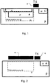
- the two implant steps comprise a deep n- implant 14 and a shallow p+ implant 16, where the p+ extends laterally beyond the n- layer in order to create an electrical connection to the substrate 12.
- a poly-silicon gate 18 is placed that enables the transfer of the charges out of the PPD region 14 to a sense node diffusion 20.
- the region around the so-called transfer gate as well as the gate itself is usually optimized with regard to the charge transport process.
- the pinned region 14 defines the photo-sensitive area 24 where photons are converted into electric charges. As long as the transfer gate 18 is set to low potential, then the photo-generated charges are stored within the PPD region 14.
- MOS gate structures usually apply a poly-silicon gate 22, which should be generally photo-transparent at least for the wavelength of interest or at least long wavelengths >500 nanometers (nm). Photons create electric charges in the area 24 of the substrate 12 beneath the gate 22 where they may be stored unless the adjacent transfer gate 18 opens the channel either to another storage gate region or to a sense node 20, as shown. While the sense node 20 is typically integrated in each pixel separately when using CMOS processes, there is only one sense node and several storage and shift registers when using CCD technology. However, the principle of the photo-sensitive element is the same in either case.
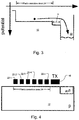
- Both types of charge domain photo-detection devices have the same drawbacks in terms of the charge handling. If the charge needs to be transferred from one photo-detecting element to another storage or sense region, the efficiency of this kind of transport process is highly dependent on the electric fields supporting this process. In extreme conditions, which are particularly the case for larger pixel sizes of, for example, greater than 1 micrometer, the photo-detecting regions do not exhibit effective lateral electric fields supporting the charge transport towards the sense node. This situation is depicted in FIG. 3 for the case that the transfer gate is set to high potential level. Due to a flat potential distribution within the sensitive region 24, single electric charges are transported to the sense node 20 by thermal movement processes, which may be some orders of magnitude slower than charge movement due to electric fields.
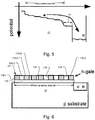
- FIG. 4 instead of a single gate across the photo-sensitive area, several adjacent gates 22-1 to 22-n are used to form a gate chain of small and narrow gates above the photosensitive area 24. By applying increasing voltages on the gates 22-1 to 22-n, a potential distribution as shown in FIG. 5 is generated. This method has proven its efficiency in practice. Compared to the method of U.S. Pat. No. 8,115,158 B2 no permanent power consumption is expected.
- the potential distribution with the semiconductor material 12 ideally looks as shown in the FIG. 5 .
- the potential increase between two gates is ideally positive. However, this depends on the potential steps applied between adjacent gates 22 and the space between two gates 22-x and 22-(x+1). The closer the gates are located to each other, the more unlikely is the generation of any potential bumps between two gates. That is the reason why in CCD processes overlapping gate structures are used where the gate-to-gate distances are typically in the nanometer range.
- the first example consists of a shaping of the n- implant layer in order to achieve a kind of pinning voltage modulation over space. This is described in Cedric Tubert et al, "High Speed Dual Port Pinned-photodiode for Time-of-Flight Imaging", IISW, 2009 .
- Another approach exploits a spatial pinning voltage modulation by applying a doping gradient for the n- implant. This is presented for example in A. Spickermann et al, "CMOS 3D image sensor based on pulse modulated time-of-flight principle and intrinsic lateral drift-field photodiode pixels", ESSCIRC, 2011 .
- CMOS active pixel sensor (APS) cell structure includes at least one transfer gate device and method of operation.
- a first transfer gate device comprises a diodic or split transfer gate conductor structure having a first doped region of first conductivity type material and a second doped region of a second conductivity type material.
- a photosensing device is formed adjacent the first doped region for collecting charge carriers in response to light incident thereto, and, a diffusion region of a second conductivity type material is formed at or below the substrate surface adjacent the second doped region of the transfer gate device for receiving charges transferred from the photosensing device while preventing spillback of charges to the photosensing device upon timed voltage bias to the diodic or split transfer gate conductor structure.
- the present invention relates to a demodulation pixel as set out in claim 1 and a method for fabricating a demodulation pixel as set out in claim 8. Other embodiments are described in the dependent claims.
- the disclosed structure enables the creation of electric drift fields while avoiding the afore-mentioned drawbacks of either PPD or gate-based approaches. For example, in some cases special requirements to the process in terms of narrow gates, overlapping gates, multi-implant step or graymask can be avoided while also avoiding potential bumps from one storage region to the next one along with a step-wise approximation of an ideal constant electric field distribution.
- the present invention concerns the creation of the drift field in a demodulation or time-of-flight pixel.
- both techniques requiring changes in the typical process - separated semi-isolated areas are created by doping a big poly-silicon gate, for example.
- the different doping regions are separated from each other via a pn-junction. Therefore this technique is called PN-Structured Gate.
- PN-structured gate is described in the context of a poly-silicon material system, other semiconductor materials are possible and not excluded.
- the invention features a demodulation pixel, comprising a substrate in which photocharges are generated and a gate layer over the substrate having one or more p-n junctions.
- the gate layer is formed in a layer, such as polysilicon, that is deposited on top of an isolation or insulation layer on the substrate.
- a sense node is located adjacent to the gate layer. This allows the movement of photocharges using toggle gates and integration gates. These have opposite doping types.
- the gate layer forms a drift and photosensitive part.
- the drift and photosensitive part provides photocharges to a demodulation part.
- the invention also features a method for fabricating a demodulation pixel, comprising: depositing a gate layer over a substrate in which photocharges are to be generated and doping the gate layer to have one or more p-n junctions.
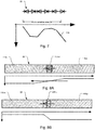
- a p-type substrate 12 is used, in the specific illustrated example. In other examples, a n-type substrate is used, however.
- a gate 22 is deposited and then patterned on the substrate 12 and electrically isolated from the substrate via an insulating layer 112.
- the single gate 22 is structured to have n- and p-doped areas 110-1 to 110-n, where the distances between those areas may vary from zero up to several micrometers.
- n- and/or p-gate regions 110-1 to 110-n By applying appropriate voltages to the n- and/or p-gate regions 110-1 to 110-n, a CCD-like control of the voltage distribution is achieved, which enables a CCD-like charge transport in the semiconductor bulk material 12.
- the every one of the areas between the n- and p-doped regions, or only a few, are lowly n- or p-type doped or intrinsic in some examples. (A few of these areas or interfaces are denoted by reference numeral 115 in Fig. 6 .)
- an n-doped sense node 20 is used. It is used to sense photo-generated charges but also to deplete the photosensitive region 24 during a reset phase.
- a buried channel is added. This involves another n-implant beneath the gate 22 and in the photosensitive region 24.
- the pn-structured gate 22 can be modeled as series of diodes as shown in Fig. 7 .
- An arbitrary voltage distribution 116 is shown, which is created by setting the diodes of the gate 22 to appropriate voltages. Currents through the gate 22 are avoided due to the fact that in any case at least one pn-junction within the current path is in reverse bias mode of operation.
- Poly-silicon layers with pn-diode structures are known. Diode characteristics have been measured depending on grain size of the poly-silicon material and optical characteristics have been exploited, see, e.g., Sooraj V. Karnik, "Lateral polysilicon p+-p-n+ and p+-n-n+ diodes", Solid-state electronics, available online at www.sciencedirect.com, 2002 ; Ming-Dou Ker et al, "Design of Negative Charge Pump Circuit with Polysilicon Diodes in a 0.25-um CMOS Process "; and S. Radovanovic et al, "High-speed lateral polysilicon photodiode in standard CMOS technology ". None of the existing publications, however, proposes poly-silicon gate with a dedicated two-dimensional pn-structuring for the control of the charge flow within the semiconductor material by adding several pn diodes in opposite directions together.
- the gate 22 is completely doped, the gate is set up as shown Fig. 8A . If both n-region 110-n as well as p-type region 110-p are contacted from outside, then the n-type area must not be more than Vdiode ⁇ 0.3V below adjacent p-type areas, otherwise a high current would start to flow. A forward-biased diode would be realized.
- n- and p-type regions In reverse-biased mode large voltage differences between n- and p-type regions may be applied, where the higher voltage is put to the n-type region. Only leakage currents are expected to flow as long as the voltage does not exceed the breakdown voltage. This characteristic voltage level is strongly depending on the characteristics of the diode such as grain size of the poly-silicon material, doping concentrations and distance between n- and p-type regions.
- Fig. 8A shows the voltage distribution for a reverse biased pn-junction with large depletion width 110-d.
- Fig. 8B shows the diode in forward bias situation, where the depletion width is smaller accordingly.
- n+/p+ drain/source doping in a CMOS process might lead to Zener diode characteristics, where reverse biasing would result in a significant current flow. This must be considered in the design of the diode by probably inserting a certain space in-between the n- and p-type regions. In this case actually a PIN diode would be realized, where the layer between the n- and p-doped regions is non-doped, possibly intrinsic silicon material. Also several extra doping steps are used in some examples.
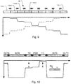
- Fig. 9 The concept for creating a drift field with the pn-structured gate technique is shown in Fig. 9 .
- Fig. 10 illustrates a demodulation region in time-of-flight pixel, according to an embodiment of the invention. It generally has a number of gates that are driven at high frequencies, usually in the MegaHertz range up to GigaHertz. They are called toggle gates TG. Typically there are two or more toggle gates TG. In the illustrated example, the toggle gates TG are constructed from p-doped polysilicon. Furthermore, the demodulation region further preferably includes a n-doped middle photogate PGM, n-doped integration gates INTG as well as p-doped outgate OUTG. While the integration gates INTG act as storage elements, the outgates OUTG are used to decouple the integration regions from a sense node region.
- the example embodiment shows two toggle gates TG on either side of the middle photogate PGM, integration gates INTG and outgates OUTG.
- the demodulation process thus, delivers 2 output samples.
- the integration gates INTG are the gates with the highest potential during integration, for example 5V. That is the reason why n-type poly-silicon has been chosen for them in this figure.
- the outgates OUTG have a relative low potential, for example 1V, to build the barrier between the integration gate and the sense node. Therefore p-type poly-silicon is used. Starting with this configuration.
- Fig. 10 also shows the potential distribution during integration and demodulation phases.
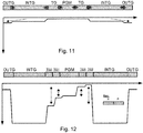
- Fig. 12 shows an alternative gate structuring allowing for even better demodulation performance, for some applications.
- the toggle gates TG1, TG2 have a double pn arrangement. Demodulation region with double toggle gates allows for higher potential steps between PGM and TGs.
- Drift field demodulation pixels as disclosed in incorporated U.S. Pat. No. 8,115,158 B2 have a drift and/or photosensitive part 24 and a demodulation part 120, as illustrated in Fig. 13 .
- the drift and/or photosensitive part 24 has a triangular shape, due to which the pixel is often referred to as a silo pixel architecture.
- a single pn-structured gate 110 is formed in the photosensitive part 24 that comprises alternative bands of n-doped polysilicon 124-1, 124-3, 124-5 and p-doped poly silicon 124-2, 124-4, 124-6.
- the gate 110 is spaced and electrically insulated from the substrate by an insulating layer as shown in Fig. 6 .
- This structure in the drift part 24 passes photogenerated charge carriers formed in the underlying substrate to modulation part 120, that comprises a middle photogate PGM, and two (left, right) toggle gates TG.
- modulation part 120 that comprises a middle photogate PGM, and two (left, right) toggle gates TG.
- photogenerated charge carriers are alternately stored into either of the left or right integration gates INTG.
- the photogenerated charges integrated in each of the left or right integration gates INTG are passed to the respective left and right sense nodes 130-L, 130-R via the respective left and right out gates OUTG.
- a dump node 136 is provided in which photogenerated charges may be flushed prior to a demodulation cycle.
- n-type base doping of the gate 15 0 and p-type semi-doped region 152 is shown in Fig. 14 . This is just an example, however, and the invention is not restricted to n-type base doping, also the opposite of p-type base doping is another option.
- the left n side 150-L is set to higher potential, e.g. 3V, than the right n side 150-R, e.g. 2V.
- the p-type region 152 is set to a lower potential, for example 1V.
- the functional principle is similar to a JFET device. Depending on the p-voltage, the channel below is more or less resistive. As a result a linear potential distribution is created at the bottom surface as shown in the figure.
- the potential of the p-type poly-silicon 152 does not directly influence the potential in the substrate but modulates the resistance between two adjacent n-type islands 150-L, 150-R. This allows for very high-ohmic connections between n-type areas; the drift field can be implemented with a high-resistive gate.
- the 'channel' is only resistive, when the potential difference is not too large. Otherwise the device may come into saturation and as a consequence the potential distribution is not linear anymore.
- Fig. 15 shows an example for generating a drift region by using two stages of p-type doping 150-L, 150-R to define three islands 150-L, 150-C, 150-R.
- the p-doped regions 152 are used to efficiently separate the different gates, separate the out gate OUTG from the integration gate INTG, separate the integration gate INTG from the toggle gate TG, and the toggle gate TG from the middle gate PGM.
- a very low potential is then applied to the p-doped regions 152.
- the p-regions 152 should be as small as possible.
- Fig. 17 shows an example of a silo drift field pixel that combines the afore-presented embodiments for a drift field and a demodulation region based on semi-doped pn-structured gate.
- a single pn-structured gate 110 is formed in the photosensitive part 24 that comprises p-doped regions 152.
- the gate 110 is spaced and electrically insulated from the substrate by an insulating layer as shown in Fig. 6 .
- This structure in the drift part 24 passes photogenerated charge carriers formed in the underlying substrate to modulation part 120, that comprises a middle photogate PGM, and two (left, right) toggle gates TG.
- modulation part 120 that comprises a middle photogate PGM, and two (left, right) toggle gates TG.
- photogenerated charge carriers are alternately stored into either of the left or right integration gates INTG.
- the photogenerated charges integrated in each of the left or right integration gates INTG are passed to the respect left and right sense nodes 130-L, 130-R via the respective left and right out gates OUTG.
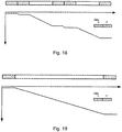
- n- and p-doped regions By pulling apart the n- and p-doped regions and creating lowly-doped or even totally undoped respectively intrinsic poly-silicon gate regions in-between, so-called PIN diode structures are created.
- the intrinsic region may be fully depleted and thus be used to create ideal constant drift fields of large lengths. There is a maximum length of intrinsic region, which depends on voltage levels, doping concentrations of n- and p-type regions, grain size of poly-silicon material etc. Several micrometers are realistic orders of length in any case.
- FIG. 18 A first example of a pn-structured gate with two intrinsic regions is shown in Fig. 18 .
- FIG. 19 Another example of a pn-structured gate is shown in Fig. 19 , where one large intrinsic region is used.
- Fig. 20 An example is shown in Fig. 20 .
- a further improvement might be achieved by pulling apart a little bit the implant regions so that the intrinsic regions in-between enable some kind of stretching of the potential drop from implant region to implant region. Graymasks would help too in order to realize different doping concentrations over space without requiring consecutive multi-implant steps.
- drift region may have a gate structure with high-low junctions and PIN diodes at the same time.
Landscapes
- Solid State Image Pick-Up Elements (AREA)
- Electrodes Of Semiconductors (AREA)
Applications Claiming Priority (2)
| Application Number | Priority Date | Filing Date | Title |
|---|---|---|---|
| US201261613363P | 2012-03-20 | 2012-03-20 | |
| PCT/IB2013/000422 WO2013140227A1 (en) | 2012-03-20 | 2013-03-20 | Pn-structured gate demodulation pixel |
Publications (2)
| Publication Number | Publication Date |
|---|---|
| EP2828891A1 EP2828891A1 (en) | 2015-01-28 |
| EP2828891B1 true EP2828891B1 (en) | 2017-03-15 |
Family
ID=48227339
Family Applications (1)
| Application Number | Title | Priority Date | Filing Date |
|---|---|---|---|
| EP13719601.0A Active EP2828891B1 (en) | 2012-03-20 | 2013-03-20 | Pn-structured gate demodulation pixel |
Country Status (7)
Families Citing this family (19)
| Publication number | Priority date | Publication date | Assignee | Title |
|---|---|---|---|---|
| US9721987B2 (en) * | 2014-02-03 | 2017-08-01 | Taiwan Semiconductor Manufacturing Co., Ltd. | Pixel with transistor gate covering photodiode |
| CN105097850B (zh) * | 2014-04-25 | 2019-03-29 | 格科微电子(上海)有限公司 | Cmos图像传感器及其制造方法 |
| GB2537421A (en) | 2015-04-17 | 2016-10-19 | Stmicroelectronics (Research & Development) Ltd | A pixel having a plurality of photodiodes |
| EP3082165B1 (en) * | 2015-04-17 | 2021-07-28 | STMicroelectronics (Research & Development) Limited | A pixel having a plurality of pinned photodiodes |
| US9860466B2 (en) * | 2015-05-14 | 2018-01-02 | Kla-Tencor Corporation | Sensor with electrically controllable aperture for inspection and metrology systems |
| CN105161462A (zh) * | 2015-07-22 | 2015-12-16 | 格科微电子(上海)有限公司 | 提高背照式图像传感器的载流子传输效率的方法 |
| US10418410B2 (en) | 2015-10-08 | 2019-09-17 | Ams Sensors Singapore Pte. Ltd. | Optoelectronic modules operable to collect spectral data and distance data |
| TWI571938B (zh) * | 2015-10-15 | 2017-02-21 | 力晶科技股份有限公司 | 半導體元件及其製造方法 |
| US10276628B2 (en) | 2016-05-17 | 2019-04-30 | Ams Sensors Singapore Pte. Ltd. | Time-of-fight pixel including in-pixel buried channel transistors |
| JP6967716B2 (ja) * | 2017-06-29 | 2021-11-17 | パナソニックIpマネジメント株式会社 | 光検出装置、及び撮像装置 |
| JP7209170B2 (ja) * | 2017-06-29 | 2023-01-20 | パナソニックIpマネジメント株式会社 | 光検出装置、及び撮像装置 |
| EP3923333B1 (en) * | 2020-03-17 | 2024-12-11 | Shenzhen Goodix Technology Co., Ltd. | Optical sensor and time of flight-based distance measurement system |
| US11742370B2 (en) | 2020-05-27 | 2023-08-29 | Microsoft Technology Licensing, Llc | Time-of-flight pixel with vertical photogates |
| CN112331688B (zh) * | 2020-11-04 | 2022-07-29 | 中国电子科技集团公司第四十四研究所 | 一种同时实现大信号处理和高频转移的ccd结构 |
| DE102020132868A1 (de) * | 2020-12-09 | 2022-06-09 | Ifm Electronic Gmbh | Lichtlaufzeitpixel mit Ladungsspeicher |
| CN112864183B (zh) * | 2021-01-18 | 2023-08-25 | 上海集成电路装备材料产业创新中心有限公司 | 一种改善传输迟滞的像元结构 |
| CN113889495A (zh) * | 2021-09-06 | 2022-01-04 | 天津大学 | 降低前馈效应的psd型传输栅图像传感器及制作方法 |
| JP7572012B2 (ja) * | 2022-08-27 | 2024-10-23 | Toppanホールディングス株式会社 | 光検出素子及び固体撮像装置 |
| CN115548138B (zh) * | 2022-08-31 | 2025-06-27 | 山东东仪光电仪器有限公司 | 低电容硅像素探测器阵列芯片及其制作方法 |
Citations (1)
| Publication number | Priority date | Publication date | Assignee | Title |
|---|---|---|---|---|
| US20090179232A1 (en) * | 2008-01-14 | 2009-07-16 | Adkisson James W | Low lag transfer gate device |
Family Cites Families (6)
| Publication number | Priority date | Publication date | Assignee | Title |
|---|---|---|---|---|
| GB2389960A (en) | 2002-06-20 | 2003-12-24 | Suisse Electronique Microtech | Four-tap demodulation pixel |
| JP4280822B2 (ja) * | 2004-02-18 | 2009-06-17 | 国立大学法人静岡大学 | 光飛行時間型距離センサ |
| US7288788B2 (en) * | 2004-12-03 | 2007-10-30 | International Business Machines Corporation | Predoped transfer gate for an image sensor |
| ATE390715T1 (de) * | 2005-10-19 | 2008-04-15 | Suisse Electronique Microtech | Einrichtung und verfahren zur demodulation von modulierten elektromagnetischen wellenfeldern |
| JP4847828B2 (ja) | 2006-09-22 | 2011-12-28 | 旭化成エレクトロニクス株式会社 | Cmosイメージセンサの製造方法 |
| US8953149B2 (en) * | 2009-02-17 | 2015-02-10 | Microsoft Corporation | CMOS three-dimensional image sensor detectors having reduced inter-gate capacitance, and enhanced modulation contrast |
-
2013
- 2013-03-20 AU AU2013237141A patent/AU2013237141B2/en active Active
- 2013-03-20 US US13/847,704 patent/US9343607B2/en active Active
- 2013-03-20 CN CN201380015395.6A patent/CN104303304B/zh active Active
- 2013-03-20 JP JP2015500994A patent/JP6127128B2/ja active Active
- 2013-03-20 KR KR1020147027729A patent/KR102094738B1/ko active Active
- 2013-03-20 EP EP13719601.0A patent/EP2828891B1/en active Active
- 2013-03-20 WO PCT/IB2013/000422 patent/WO2013140227A1/en active Application Filing
Patent Citations (1)
| Publication number | Priority date | Publication date | Assignee | Title |
|---|---|---|---|---|
| US20090179232A1 (en) * | 2008-01-14 | 2009-07-16 | Adkisson James W | Low lag transfer gate device |
Also Published As
| Publication number | Publication date |
|---|---|
| JP6127128B2 (ja) | 2017-05-10 |
| US20130248938A1 (en) | 2013-09-26 |
| WO2013140227A1 (en) | 2013-09-26 |
| AU2013237141B2 (en) | 2016-05-12 |
| KR20140146088A (ko) | 2014-12-24 |
| CN104303304B (zh) | 2017-10-03 |
| CN104303304A (zh) | 2015-01-21 |
| JP2015512562A (ja) | 2015-04-27 |
| US9343607B2 (en) | 2016-05-17 |
| KR102094738B1 (ko) | 2020-03-31 |
| EP2828891A1 (en) | 2015-01-28 |
| AU2013237141A1 (en) | 2014-08-21 |
Similar Documents
| Publication | Publication Date | Title |
|---|---|---|
| EP2828891B1 (en) | Pn-structured gate demodulation pixel | |
| US10985201B2 (en) | Image sensor including silicon over germanium layer | |
| TWI740769B (zh) | 光學感測器 | |
| US10014340B2 (en) | Stacked SPAD image sensor | |
| CN104779259B (zh) | 用于互补金属氧化物半导体堆叠式芯片应用的单光子雪崩二极管成像传感器 | |
| CN110431441B (zh) | 用于调制的图像捕获的系统和方法 | |
| CN108140653B (zh) | 具有jfet源极跟随器的图像传感器和图像传感器像素 | |
| US10020329B2 (en) | Image sensor with solar cell function | |
| JP2008527702A (ja) | 半導体フォトダイオードおよび製造の方法 | |
| JP6351097B2 (ja) | 電磁波検出素子及び固体撮像装置 | |
| US9923014B2 (en) | Image sensor and method of manufacturing the same | |
| EP3655991B1 (en) | Back side illuminated photodetector for cmos imaging sensor with photoactive layer in a cavity | |
| CN115529429A (zh) | 图像感测装置 | |
| CN115714926A (zh) | 图像感测装置 |
Legal Events
| Date | Code | Title | Description |
|---|---|---|---|
| PUAI | Public reference made under article 153(3) epc to a published international application that has entered the european phase |
Free format text: ORIGINAL CODE: 0009012 |
|
| 17P | Request for examination filed |
Effective date: 20140814 |
|
| AK | Designated contracting states |
Kind code of ref document: A1 Designated state(s): AL AT BE BG CH CY CZ DE DK EE ES FI FR GB GR HR HU IE IS IT LI LT LU LV MC MK MT NL NO PL PT RO RS SE SI SK SM TR |
|
| AX | Request for extension of the european patent |
Extension state: BA ME |
|
| DAX | Request for extension of the european patent (deleted) | ||
| RAP1 | Party data changed (applicant data changed or rights of an application transferred) |
Owner name: HEPTAGON MICRO OPTICS PTE. LTD. |
|
| 17Q | First examination report despatched |
Effective date: 20160303 |
|
| GRAP | Despatch of communication of intention to grant a patent |
Free format text: ORIGINAL CODE: EPIDOSNIGR1 |
|
| INTG | Intention to grant announced |
Effective date: 20161014 |
|
| GRAJ | Information related to disapproval of communication of intention to grant by the applicant or resumption of examination proceedings by the epo deleted |
Free format text: ORIGINAL CODE: EPIDOSDIGR1 |
|
| STAA | Information on the status of an ep patent application or granted ep patent |
Free format text: STATUS: EXAMINATION IS IN PROGRESS |
|
| GRAR | Information related to intention to grant a patent recorded |
Free format text: ORIGINAL CODE: EPIDOSNIGR71 |
|
| GRAS | Grant fee paid |
Free format text: ORIGINAL CODE: EPIDOSNIGR3 |
|
| STAA | Information on the status of an ep patent application or granted ep patent |
Free format text: STATUS: GRANT OF PATENT IS INTENDED |
|
| GRAA | (expected) grant |
Free format text: ORIGINAL CODE: 0009210 |
|
| STAA | Information on the status of an ep patent application or granted ep patent |
Free format text: STATUS: THE PATENT HAS BEEN GRANTED |
|
| INTC | Intention to grant announced (deleted) | ||
| REG | Reference to a national code |
Ref country code: FR Ref legal event code: PLFP Year of fee payment: 5 |
|
| AK | Designated contracting states |
Kind code of ref document: B1 Designated state(s): AL AT BE BG CH CY CZ DE DK EE ES FI FR GB GR HR HU IE IS IT LI LT LU LV MC MK MT NL NO PL PT RO RS SE SI SK SM TR |
|
| INTG | Intention to grant announced |
Effective date: 20170206 |
|
| REG | Reference to a national code |
Ref country code: CH Ref legal event code: EP Ref country code: GB Ref legal event code: FG4D |
|
| REG | Reference to a national code |
Ref country code: IE Ref legal event code: FG4D |
|
| REG | Reference to a national code |
Ref country code: AT Ref legal event code: REF Ref document number: 876361 Country of ref document: AT Kind code of ref document: T Effective date: 20170415 |
|
| REG | Reference to a national code |
Ref country code: DE Ref legal event code: R096 Ref document number: 602013018556 Country of ref document: DE |
|
| REG | Reference to a national code |
Ref country code: NL Ref legal event code: FP |
|
| REG | Reference to a national code |
Ref country code: LT Ref legal event code: MG4D |
|
| PG25 | Lapsed in a contracting state [announced via postgrant information from national office to epo] |
Ref country code: NO Free format text: LAPSE BECAUSE OF FAILURE TO SUBMIT A TRANSLATION OF THE DESCRIPTION OR TO PAY THE FEE WITHIN THE PRESCRIBED TIME-LIMIT Effective date: 20170615 Ref country code: HR Free format text: LAPSE BECAUSE OF FAILURE TO SUBMIT A TRANSLATION OF THE DESCRIPTION OR TO PAY THE FEE WITHIN THE PRESCRIBED TIME-LIMIT Effective date: 20170315 Ref country code: LT Free format text: LAPSE BECAUSE OF FAILURE TO SUBMIT A TRANSLATION OF THE DESCRIPTION OR TO PAY THE FEE WITHIN THE PRESCRIBED TIME-LIMIT Effective date: 20170315 Ref country code: GR Free format text: LAPSE BECAUSE OF FAILURE TO SUBMIT A TRANSLATION OF THE DESCRIPTION OR TO PAY THE FEE WITHIN THE PRESCRIBED TIME-LIMIT Effective date: 20170616 |
|
| PG25 | Lapsed in a contracting state [announced via postgrant information from national office to epo] |
Ref country code: SE Free format text: LAPSE BECAUSE OF FAILURE TO SUBMIT A TRANSLATION OF THE DESCRIPTION OR TO PAY THE FEE WITHIN THE PRESCRIBED TIME-LIMIT Effective date: 20170315 Ref country code: RS Free format text: LAPSE BECAUSE OF FAILURE TO SUBMIT A TRANSLATION OF THE DESCRIPTION OR TO PAY THE FEE WITHIN THE PRESCRIBED TIME-LIMIT Effective date: 20170315 Ref country code: BG Free format text: LAPSE BECAUSE OF FAILURE TO SUBMIT A TRANSLATION OF THE DESCRIPTION OR TO PAY THE FEE WITHIN THE PRESCRIBED TIME-LIMIT Effective date: 20170615 Ref country code: LV Free format text: LAPSE BECAUSE OF FAILURE TO SUBMIT A TRANSLATION OF THE DESCRIPTION OR TO PAY THE FEE WITHIN THE PRESCRIBED TIME-LIMIT Effective date: 20170315 |
|
| PG25 | Lapsed in a contracting state [announced via postgrant information from national office to epo] |
Ref country code: CZ Free format text: LAPSE BECAUSE OF FAILURE TO SUBMIT A TRANSLATION OF THE DESCRIPTION OR TO PAY THE FEE WITHIN THE PRESCRIBED TIME-LIMIT Effective date: 20170315 Ref country code: IT Free format text: LAPSE BECAUSE OF FAILURE TO SUBMIT A TRANSLATION OF THE DESCRIPTION OR TO PAY THE FEE WITHIN THE PRESCRIBED TIME-LIMIT Effective date: 20170315 Ref country code: RO Free format text: LAPSE BECAUSE OF FAILURE TO SUBMIT A TRANSLATION OF THE DESCRIPTION OR TO PAY THE FEE WITHIN THE PRESCRIBED TIME-LIMIT Effective date: 20170315 Ref country code: EE Free format text: LAPSE BECAUSE OF FAILURE TO SUBMIT A TRANSLATION OF THE DESCRIPTION OR TO PAY THE FEE WITHIN THE PRESCRIBED TIME-LIMIT Effective date: 20170315 Ref country code: SK Free format text: LAPSE BECAUSE OF FAILURE TO SUBMIT A TRANSLATION OF THE DESCRIPTION OR TO PAY THE FEE WITHIN THE PRESCRIBED TIME-LIMIT Effective date: 20170315 Ref country code: ES Free format text: LAPSE BECAUSE OF FAILURE TO SUBMIT A TRANSLATION OF THE DESCRIPTION OR TO PAY THE FEE WITHIN THE PRESCRIBED TIME-LIMIT Effective date: 20170315 |
|
| PG25 | Lapsed in a contracting state [announced via postgrant information from national office to epo] |
Ref country code: SM Free format text: LAPSE BECAUSE OF FAILURE TO SUBMIT A TRANSLATION OF THE DESCRIPTION OR TO PAY THE FEE WITHIN THE PRESCRIBED TIME-LIMIT Effective date: 20170315 Ref country code: IS Free format text: LAPSE BECAUSE OF FAILURE TO SUBMIT A TRANSLATION OF THE DESCRIPTION OR TO PAY THE FEE WITHIN THE PRESCRIBED TIME-LIMIT Effective date: 20170715 Ref country code: PT Free format text: LAPSE BECAUSE OF FAILURE TO SUBMIT A TRANSLATION OF THE DESCRIPTION OR TO PAY THE FEE WITHIN THE PRESCRIBED TIME-LIMIT Effective date: 20170717 Ref country code: PL Free format text: LAPSE BECAUSE OF FAILURE TO SUBMIT A TRANSLATION OF THE DESCRIPTION OR TO PAY THE FEE WITHIN THE PRESCRIBED TIME-LIMIT Effective date: 20170315 |
|
| REG | Reference to a national code |
Ref country code: DE Ref legal event code: R097 Ref document number: 602013018556 Country of ref document: DE |
|
| REG | Reference to a national code |
Ref country code: IE Ref legal event code: MM4A |
|
| PLBE | No opposition filed within time limit |
Free format text: ORIGINAL CODE: 0009261 |
|
| STAA | Information on the status of an ep patent application or granted ep patent |
Free format text: STATUS: NO OPPOSITION FILED WITHIN TIME LIMIT |
|
| PG25 | Lapsed in a contracting state [announced via postgrant information from national office to epo] |
Ref country code: MC Free format text: LAPSE BECAUSE OF FAILURE TO SUBMIT A TRANSLATION OF THE DESCRIPTION OR TO PAY THE FEE WITHIN THE PRESCRIBED TIME-LIMIT Effective date: 20170315 Ref country code: LU Free format text: LAPSE BECAUSE OF NON-PAYMENT OF DUE FEES Effective date: 20170320 Ref country code: DK Free format text: LAPSE BECAUSE OF FAILURE TO SUBMIT A TRANSLATION OF THE DESCRIPTION OR TO PAY THE FEE WITHIN THE PRESCRIBED TIME-LIMIT Effective date: 20170315 |
|
| 26N | No opposition filed |
Effective date: 20171218 |
|
| REG | Reference to a national code |
Ref country code: FR Ref legal event code: PLFP Year of fee payment: 6 |
|
| PG25 | Lapsed in a contracting state [announced via postgrant information from national office to epo] |
Ref country code: IE Free format text: LAPSE BECAUSE OF NON-PAYMENT OF DUE FEES Effective date: 20170320 Ref country code: SI Free format text: LAPSE BECAUSE OF FAILURE TO SUBMIT A TRANSLATION OF THE DESCRIPTION OR TO PAY THE FEE WITHIN THE PRESCRIBED TIME-LIMIT Effective date: 20170315 |
|
| REG | Reference to a national code |
Ref country code: BE Ref legal event code: MM Effective date: 20170331 |
|
| PG25 | Lapsed in a contracting state [announced via postgrant information from national office to epo] |
Ref country code: BE Free format text: LAPSE BECAUSE OF NON-PAYMENT OF DUE FEES Effective date: 20170331 |
|
| REG | Reference to a national code |
Ref country code: DE Ref legal event code: R082 Ref document number: 602013018556 Country of ref document: DE Representative=s name: PROCK, THOMAS, DR., GB Ref country code: DE Ref legal event code: R082 Ref document number: 602013018556 Country of ref document: DE Representative=s name: FISH & RICHARDSON P.C., DE |
|
| PG25 | Lapsed in a contracting state [announced via postgrant information from national office to epo] |
Ref country code: MT Free format text: LAPSE BECAUSE OF NON-PAYMENT OF DUE FEES Effective date: 20170320 |
|
| PG25 | Lapsed in a contracting state [announced via postgrant information from national office to epo] |
Ref country code: HU Free format text: LAPSE BECAUSE OF FAILURE TO SUBMIT A TRANSLATION OF THE DESCRIPTION OR TO PAY THE FEE WITHIN THE PRESCRIBED TIME-LIMIT; INVALID AB INITIO Effective date: 20130320 |
|
| REG | Reference to a national code |
Ref country code: AT Ref legal event code: UEP Ref document number: 876361 Country of ref document: AT Kind code of ref document: T Effective date: 20170315 |
|
| PG25 | Lapsed in a contracting state [announced via postgrant information from national office to epo] |
Ref country code: CY Free format text: LAPSE BECAUSE OF FAILURE TO SUBMIT A TRANSLATION OF THE DESCRIPTION OR TO PAY THE FEE WITHIN THE PRESCRIBED TIME-LIMIT Effective date: 20170315 |
|
| PG25 | Lapsed in a contracting state [announced via postgrant information from national office to epo] |
Ref country code: MK Free format text: LAPSE BECAUSE OF FAILURE TO SUBMIT A TRANSLATION OF THE DESCRIPTION OR TO PAY THE FEE WITHIN THE PRESCRIBED TIME-LIMIT Effective date: 20170315 |
|
| PG25 | Lapsed in a contracting state [announced via postgrant information from national office to epo] |
Ref country code: TR Free format text: LAPSE BECAUSE OF FAILURE TO SUBMIT A TRANSLATION OF THE DESCRIPTION OR TO PAY THE FEE WITHIN THE PRESCRIBED TIME-LIMIT Effective date: 20170315 |
|
| REG | Reference to a national code |
Ref country code: DE Ref legal event code: R082 Ref document number: 602013018556 Country of ref document: DE Representative=s name: VIERING, JENTSCHURA & PARTNER MBB PATENT- UND , DE Ref country code: DE Ref legal event code: R082 Ref document number: 602013018556 Country of ref document: DE Representative=s name: PROCK, THOMAS, DR., GB |
|
| PG25 | Lapsed in a contracting state [announced via postgrant information from national office to epo] |
Ref country code: AL Free format text: LAPSE BECAUSE OF FAILURE TO SUBMIT A TRANSLATION OF THE DESCRIPTION OR TO PAY THE FEE WITHIN THE PRESCRIBED TIME-LIMIT Effective date: 20170315 |
|
| P01 | Opt-out of the competence of the unified patent court (upc) registered |
Effective date: 20230825 |
|
| PGFP | Annual fee paid to national office [announced via postgrant information from national office to epo] |
Ref country code: AT Payment date: 20240321 Year of fee payment: 12 |
|
| PGFP | Annual fee paid to national office [announced via postgrant information from national office to epo] |
Ref country code: FI Payment date: 20240320 Year of fee payment: 12 |
|
| REG | Reference to a national code |
Ref country code: DE Ref legal event code: R082 Ref document number: 602013018556 Country of ref document: DE Representative=s name: VIERING, JENTSCHURA & PARTNER MBB PATENT- UND , DE |
|
| PGFP | Annual fee paid to national office [announced via postgrant information from national office to epo] |
Ref country code: CH Payment date: 20240401 Year of fee payment: 12 |
|
| REG | Reference to a national code |
Ref country code: DE Ref legal event code: R081 Ref document number: 602013018556 Country of ref document: DE Owner name: AMS-OSRAM ASIA PACIFIC PTE. LTD., SG Free format text: FORMER OWNER: HEPTAGON MICRO OPTICS PTE. LTD., SINGAPORE, SG |
|
| REG | Reference to a national code |
Ref country code: NL Ref legal event code: HC Owner name: AMS-OSRAM ASIA PACIFIC PTE. LTD.; SG Free format text: DETAILS ASSIGNMENT: CHANGE OF OWNER(S), CHANGE OF OWNER(S) NAME; FORMER OWNER NAME: HEPTAGON MICRO OPTICS PTE. LTD. Effective date: 20240830 |
|
| REG | Reference to a national code |
Ref country code: DE Ref legal event code: R079 Ref document number: 602013018556 Country of ref document: DE Free format text: PREVIOUS MAIN CLASS: H01L0027146000 Ipc: H10F0039180000 |
|
| PGFP | Annual fee paid to national office [announced via postgrant information from national office to epo] |
Ref country code: DE Payment date: 20250319 Year of fee payment: 13 |
|
| PGFP | Annual fee paid to national office [announced via postgrant information from national office to epo] |
Ref country code: NL Payment date: 20250319 Year of fee payment: 13 |
|
| PGFP | Annual fee paid to national office [announced via postgrant information from national office to epo] |
Ref country code: FR Payment date: 20250325 Year of fee payment: 13 |
|
| PGFP | Annual fee paid to national office [announced via postgrant information from national office to epo] |
Ref country code: GB Payment date: 20250321 Year of fee payment: 13 |
|
| REG | Reference to a national code |
Ref country code: AT Ref legal event code: HC Ref document number: 876361 Country of ref document: AT Kind code of ref document: T Owner name: AMS-OSRAM ASIA PACIFIC PTE. LTD., SG Effective date: 20250424 |