EP2825856B1 - Capacitive micro-machined ultrasound transducer device with charging voltage source - Google Patents
Capacitive micro-machined ultrasound transducer device with charging voltage source Download PDFInfo
- Publication number
- EP2825856B1 EP2825856B1 EP13717563.4A EP13717563A EP2825856B1 EP 2825856 B1 EP2825856 B1 EP 2825856B1 EP 13717563 A EP13717563 A EP 13717563A EP 2825856 B1 EP2825856 B1 EP 2825856B1
- Authority
- EP
- European Patent Office
- Prior art keywords
- charging voltage
- cmut
- dielectric layer
- voltage source
- electrode
- Prior art date
- Legal status (The legal status is an assumption and is not a legal conclusion. Google has not performed a legal analysis and makes no representation as to the accuracy of the status listed.)
- Active
Links
- 238000002604 ultrasonography Methods 0.000 title claims description 60
- 239000012528 membrane Substances 0.000 claims description 37
- 238000012544 monitoring process Methods 0.000 claims description 36
- 230000035945 sensitivity Effects 0.000 claims description 27
- 239000000758 substrate Substances 0.000 claims description 23
- 238000000034 method Methods 0.000 claims description 14
- 238000004519 manufacturing process Methods 0.000 claims description 11
- 230000002441 reversible effect Effects 0.000 claims description 9
- 238000009825 accumulation Methods 0.000 claims description 3
- 239000002800 charge carrier Substances 0.000 claims description 3
- 230000000694 effects Effects 0.000 description 16
- 238000010586 diagram Methods 0.000 description 6
- 239000003990 capacitor Substances 0.000 description 3
- 230000001419 dependent effect Effects 0.000 description 3
- 238000012285 ultrasound imaging Methods 0.000 description 3
- 238000002679 ablation Methods 0.000 description 2
- 238000003491 array Methods 0.000 description 2
- 230000001186 cumulative effect Effects 0.000 description 2
- 230000003247 decreasing effect Effects 0.000 description 2
- 238000002592 echocardiography Methods 0.000 description 2
- 238000003384 imaging method Methods 0.000 description 2
- 230000001717 pathogenic effect Effects 0.000 description 2
- 229920001296 polysiloxane Polymers 0.000 description 2
- 239000004065 semiconductor Substances 0.000 description 2
- 230000001225 therapeutic effect Effects 0.000 description 2
- 230000005540 biological transmission Effects 0.000 description 1
- 230000015556 catabolic process Effects 0.000 description 1
- 230000000295 complement effect Effects 0.000 description 1
- 238000010276 construction Methods 0.000 description 1
- 230000008878 coupling Effects 0.000 description 1
- 238000010168 coupling process Methods 0.000 description 1
- 238000005859 coupling reaction Methods 0.000 description 1
- 239000013078 crystal Substances 0.000 description 1
- 230000001939 inductive effect Effects 0.000 description 1
- 238000002955 isolation Methods 0.000 description 1
- 230000000670 limiting effect Effects 0.000 description 1
- 239000011159 matrix material Substances 0.000 description 1
- 238000004377 microelectronic Methods 0.000 description 1
- 150000004767 nitrides Chemical class 0.000 description 1
- 230000002829 reductive effect Effects 0.000 description 1
- 230000008054 signal transmission Effects 0.000 description 1
- 229910052814 silicon oxide Inorganic materials 0.000 description 1
- 230000003068 static effect Effects 0.000 description 1
- 230000002463 transducing effect Effects 0.000 description 1
- 230000001131 transforming effect Effects 0.000 description 1
- 230000005641 tunneling Effects 0.000 description 1
Images


Classifications
-
- B—PERFORMING OPERATIONS; TRANSPORTING
- B06—GENERATING OR TRANSMITTING MECHANICAL VIBRATIONS IN GENERAL
- B06B—METHODS OR APPARATUS FOR GENERATING OR TRANSMITTING MECHANICAL VIBRATIONS OF INFRASONIC, SONIC, OR ULTRASONIC FREQUENCY, e.g. FOR PERFORMING MECHANICAL WORK IN GENERAL
- B06B1/00—Methods or apparatus for generating mechanical vibrations of infrasonic, sonic, or ultrasonic frequency
- B06B1/02—Methods or apparatus for generating mechanical vibrations of infrasonic, sonic, or ultrasonic frequency making use of electrical energy
- B06B1/0292—Electrostatic transducers, e.g. electret-type
-
- G—PHYSICS
- G01—MEASURING; TESTING
- G01N—INVESTIGATING OR ANALYSING MATERIALS BY DETERMINING THEIR CHEMICAL OR PHYSICAL PROPERTIES
- G01N29/00—Investigating or analysing materials by the use of ultrasonic, sonic or infrasonic waves; Visualisation of the interior of objects by transmitting ultrasonic or sonic waves through the object
- G01N29/22—Details, e.g. general constructional or apparatus details
- G01N29/24—Probes
- G01N29/2406—Electrostatic or capacitive probes, e.g. electret or cMUT-probes
Definitions
- the present invention relates to a capacitive micro-machined ultrasound transducer device (CMUT) device for transmitting and/or receiving ultrasound and to a method of operating the same.
- CMUT capacitive micro-machined ultrasound transducer device
- the present invention can for example be used in a medical ultrasound system (e.g. diagnostic or therapeutic medical ultrasound system), in particular with ultrasound imaging functionality.
- the heart of any ultrasound (imaging) system is the transducer device with its transducer elements or transducer cells which convert electrical energy in acoustic energy and back.
- these transducer elements or transducer cells are made from piezoelectric crystals arranged in linear (1-D) transducer arrays, and operating at frequencies up to 10 MHz.
- matrix (2-D) transducer arrays and the drive towards miniaturization to integrate ultrasound (imaging) functionality into catheters and guide wires has resulted in the development of so-called capacitive micro-machined ultrasound transducer (CMUT) devices.
- CMUT capacitive micro-machined ultrasound transducer
- a CMUT cell comprises a membrane (or diaphragm), a cavity underneath the membrane, and electrodes forming a capacitor.
- ultrasound waves For receiving ultrasound waves, ultrasound waves cause the membrane to move or vibrate and the variation and capacitance between the electrodes can be detected. Thereby, the ultrasound waves are transformed into a corresponding electrical signal.
- an electrical signal applied to the electrodes causes the membrane to move or vibrate and thereby transmitting ultrasound waves.
- the electric signal or voltage causes the membrane to deflect, thereby creating ultrasound pressure waves.
- a CMUT cell is manufactured using microelectronic semiconductor fabrication techniques.
- CMUT device offers advantages in terms of frequency coverage and ease of fabrication over contemporary piezoelectric transducer devices. However, CMUT devices currently may still have a disadvantage in terms of the efficiency and acoustic pressure output relative to existing piezoelectric transducer devices.
- an operating bias voltage applied or supplied between the electrodes can be increased.
- the operating bias voltage that can be applied due to dielectric breakdown and charged tunneling effects.
- the operating bias voltage due to driving circuitry, for example in the form of an application specific integrated circuit (ASIC).
- a problem with applying an increased or excessive operating bias voltage can be that the membrane collapses to the substrate and thereby the electrodes may electrically contact each other.
- the CMUT cell can comprise a dielectric layer or dielectric layers between the electrodes.
- a first dielectric layer on or as part of the substrate and a second dielectric layer on or as part of the membrane can be used.
- US 2010/0237807 A1 discloses a system and method for biasing a capacitive ultrasonic transducer (CMUT) device with a circuit that includes a CMUT that includes a first plate and a second plate that form a membrane structure; a circuit voltage source at a complementary metal-oxide-semiconductor (CMOS) compatible voltage; a bias voltage source that applies a bias voltage greater than a CMOS compatible voltage and is applied to the first plate; and readout electronics with an input connected on the second plate side of the circuit.
- the bias voltage alternates polarity according to events related to receiving or transmission of a signal.
- a bias source may be used that alternates polarity periodically during the ultrasound imaging procedure, as opposed to a DC bias source. This may be used to resolve the charging problems that arise while holding CMUTs at constant DC bias.
- US 2009/0301199 A1 discloses an ultrasound array trasnducer having a charge control for controlling a charge in the transducer. This allows sensitivity variation to be calibrated.
- US 2010/254222 A1 describes a CMUT having a transmission mode and a reception mode.
- the CMUT switches mode based on whether a spring member in the CMUT contacts an opposing surface at a contact point in the CMUT.
- US 2007/140515 A1 discloses a concept of dissipating static charge in a capactive membrance trasnducer using light exposure, such as ultraviolet light.
- CMUT capacitive micro-machined ultrasound transducer
- CMUT capacitive micro-machined ultrasound transducer
- the term operating bias voltage describes a bias voltage supplied during an operation phase of the CMUT device, i.e. during transmitting and/or receiving of ultrasound waves.
- the additional charging voltage is in particular not supplied during an operation phase, i.e. not during transmitting and/or receiving of ultrasound waves. For example, if first an additional charging voltage is supplied or applied and then the operating bias voltage during an operation phase has the reverse polarity to the charging voltage, the output pressure or receive sensitivity of the device can be significantly increased (e.g. by a factor of two or more). Therefore, the effect of charges in the dielectric layer(s) (charging effect) is used to increase output pressure or receive sensitivity.
- a semi-permanent voltage is effectively impressed on the electrodes of the CMUT device.
- This semi-permanent voltage is caused by charge carriers trapped in the dielectric layer(s) so they do not quickly bleed off. This voltage essentially adds to any applied operating bias voltage, thus allowing higher effective forces on the membrane for a given externally applied voltage.
- the CMUT device further comprises a control unit for controlling the operating bias voltage source and/or the charging voltage source to control the charge in the at least one dielectric layer.
- a control unit for controlling the operating bias voltage source and/or the charging voltage source to control the charge in the at least one dielectric layer. This is in particular necessary if it is found that the charge cannot be permanently maintained in the dielectric layer(s). In this way, the additional charging voltage can be supplied when actually using the device, as opposed to manufacturing the device.
- the control unit can be implemented in a driving circuitry, such as an ASIC, of the CMUT device. In this way, the costs of the device are not substantially increased.
- control unit is adapted to control the operating bias voltage source to supply the operating bias voltage for a first time period during transmitting and/or receiving ultrasound waves.
- control unit is adapted to control the charging voltage source to supply the charging voltage for a second time period during no transmitting and/or receiving of ultrasound waves.
- the second time period is before the first time period.
- the second time period is after the first time period.
- the second time period is in between two first time periods.
- control unit is adapted to control the charging voltage source to supply the charging voltage periodically.
- the charging voltage can be supplied before each scan line or before each frame.
- the device is intentionally charged in such a way as to increase output pressure and/or receive sensitivity during subsequent operation. In this way it is ensured that the output pressure and/or receive sensitivity is increased permanently. This increases performance and/or reliability of the device.
- control unit is adapted to control the operating bias voltage source to supply the operating bias voltage at a first voltage level, and to control the charging voltage source to supply the charging voltage at a second voltage level different from the first voltage level.
- the voltage level of the charging voltage does not need to be the same as the voltage level of the operating bias voltage. This increases flexibility of the device.
- the second voltage level can be smaller than the first voltage level. In an alternative example, the second voltage level can be greater than the first voltage level.
- the CMUT device further comprises a monitoring unit for monitoring the charge in the at least one dielectric layer.
- a monitoring unit for monitoring the charge in the at least one dielectric layer.
- the monitoring unit can be implemented in a driving circuitry, such as an ASIC, of the CMUT device. In this way, the costs of the device are not substantially increased.
- the monitoring unit is adapted to detect when the charge in the at least one dielectric layer is below a predefined value, i.e. insufficient. In this way it can be monitored or checked if the charge in the dielectric layer(s) has become insufficient so that an action needs to be taken. This improves reliability of the device.
- the monitoring unit can be adapted to compare the currently monitored charge with a predefined value.
- the current shift in the capacitance-versus-voltage curve can be compared with a predefined value.
- the current output pressure and/or receive sensitivity can be compared with a predefined value.
- the control unit is adapted to control the charging voltage source to reapply the charging voltage when the monitoring unit detects that the charge in the at least one dielectric layer is insufficient. In this way the charge in the dielectric layer(s) can be refreshed over the useful life of the CMUT device. This enables to sustain improved output pressure and/or receive sensitivity. In this way the performance and/or reliability of the device are increased. For example, the CMUT device can be in its normal operation until a time, when the output pressure and/or receive sensitivity has decreased and the CMUT device needs to be charged again with the charging voltage to achieve the desired output pressure and/or receive sensitivity.
- control unit and the monitoring unit are implemented in the same device.
- control unit and the monitoring unit can be implemented in a driving circuitry, such as an ASIC, of the CMUT device. In this way, the costs of the device are not substantially increased.
- the CMUT device further comprises an alternating current source for supplying an alternating current between the first and second electrode for transmitting ultrasound waves.
- an alternating current source for supplying an alternating current between the first and second electrode for transmitting ultrasound waves.
- a conventional CMUT device is provided which transmits ultrasound waves (or pulses) and then receives the echoes of the transmitted ultrasound waves (or pulses).
- the alternating current source can be controlled by a driving circuitry, such as an ASIC, of the device in a conventional manner.
- the CMUT device is a high-intensity focused ultrasound (HIFU) transducer device.
- HIFU high-intensity focused ultrasound
- a HIFU transducer device can for example be used in a medical system to heat and destroy pathogenic tissue rapidly through ablation.
- the operating bias voltage source and the charging voltage source are implemented in one single voltage source. This reduces costs of the device.
- the bias voltage source and the charging voltage source are implemented as separate voltage sources. This increases flexibility of the device. For example, two different voltage levels can be implemented in this way.
- Fig. 1 shows a schematic cross-sectional view of a typical CMUT cell 10.
- the CMUT transducer cell 10 is normally fabricated along with a plurality of similar adjacent cells on a substrate 13.
- the substrate 13 comprises a substrate base layer 12.
- a diaphragm or membrane 15 is supported above the substrate by an insulating support 16. In this way a cavity 18 is formed between the membrane 15 and the substrate 13.
- the membrane 15 comprises a membrane base layer 14.
- the cavity 18 between the membrane and the substrate may be air or gas-filled or wholly or partially evacuated.
- a conductive film or layer forms a first electrode 22 in the substrate 13, and a similar film or layer forms a second electrode 20 in the membrane 15. These two electrodes 20, 22, separated by the cavity 18, form a capacitance or capacitor.
- ultrasound waves in form of an acoustic signal cause the membrane 15 to vibrate the variation in the capacitance can be detected, thereby transducing or transforming the ultrasound waves into a corresponding electrical signal.
- an alternating current (AC) or AC signal applied to the electrodes 20, 22 will modulate the capacitance, causing the membrane to move and thereby transmit ultrasound waves as an acoustic signal.
- ultrasound waves cause the membrane 15 to move or vibrate and the variation and capacitance between the electrodes 20, 22 can be detected. Thereby, the ultrasound waves are transformed into a corresponding electrical signal.
- an electrical signal applied to the electrodes 20, 22 causes the membrane to move or vibrate and thereby transmitting ultrasound waves.
- CMUT is inherently a quadratic device so that the acoustic signal is normally the harmonic of the applied signal, that is, the acoustic signal will be at twice the frequency of the applied electrical signal frequency.
- a bias voltage is typically applied to the two electrodes 20, 22 which causes the membrane 15 to be attracted to the substrate 13 by the resulting coulombic force.
- Fig. 2 shows a schematic illustration of the electrical properties of a typical CMUT cell.
- a CMUT cell is schematically shown where a DC bias voltage V B is applied to a bias terminal 24 and is coupled to the membrane electrode 20 by a path which poses a high impedance Z to AC signals, such as an inductive impedance.
- the membrane 15 can contact the substrate 13, short-circuiting the device as the two electrodes or plates of the device are stuck together by VanderWals forces. This sticking can occur when the CMUT cell is overdriven, and can vary from one device to another with the same bias voltage V B due to manufacturing tolerance variations.
- Permanent sticking can be reduced be providing an electrical isolation layer or dielectric layer between the electrodes 20, 22 or by embedding the electrodes 20, 22 therein.
- a so-called ONO dielectric layer made of layers of silicone oxide - silicone nitride - silicon oxide
- WO 2010/032156 A2 can be used, as for example disclosed in WO 2010/032156 A2 .
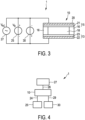
- CMUT device 1 shows a CMUT device 1 according to an embodiment.
- Fig. 4 shows a schematic block diagram of a CMUT device 1 according to a first embodiment, in particular the embodiment of Fig. 3 .
- the CMUT device 1 comprises a CMUT cell 10 which comprises a substrate 13 comprising a first electrode 22, a membrane 15 comprising a second electrode 20, at least one dielectric layer 21, 23 between the first electrode 22 and the second electrode 20, and a cavity 18 formed between the substrate 13 and the membrane 15.
- CMUT cell 10 which comprises a substrate 13 comprising a first electrode 22, a membrane 15 comprising a second electrode 20, at least one dielectric layer 21, 23 between the first electrode 22 and the second electrode 20, and a cavity 18 formed between the substrate 13 and the membrane 15.
- the CMUT cell 10 comprises a first dielectric layer 23 and a second dielectric layer 21.
- the substrate 13 comprises the first dielectric layer 23 and the membrane comprises the second dielectric layer 21.
- the electrodes 20, 22 could each be embedded in a dielectric layer.
- the CMUT device 1 comprises an alternating current (AC) source 27 for supplying an alternating current or AC signal between the first and second electrode 22, 20 for transmitting ultrasound waves.
- the AC source 27 is connected to the electrodes 20, 22 of the CMUT cell 10 through an AC signal terminal or connection 26.
- the CMUT device 1 transmits ultrasound waves (or pulses) when an alternating current or AC signal is supplied to the electrodes 20, 22 of the CMUT cell 10, and then the CMUT device 1 receives the echoes of the transmitted ultrasound waves (or pulses).
- the alternating current source 27 can be controlled by an ASIC of the device.
- this charging voltage source 30 By using this charging voltage source 30 the effect of trapped charges in the dielectric layer(s) can be used to increase output pressure and/or receive sensitivity of the CMUT device, in particular by supplying or applying an additional or intentional charging voltage Vc between the electrodes 20, 22 having the reverse (or opposite) polarity of the polarity of the usual operating bias voltage V B .
- bias voltage source 25 and the charging voltage source 30 can be implemented as separate voltage sources, as indicated in Fig. 3 and Fig. 4 . This increases flexibility of the device. However, it will be understood that the operating bias voltage source and the charging voltage source could also be implemented in one single voltage source.
- the method comprises the step of supplying an operating bias voltage V B of a first polarity between the first and second electrode 20, 22 during transmitting and/or receiving ultrasound waves, in particular using the operating bias voltage source 25, and the step of supplying an additional charging voltage Vc between the first and second electrode, in particular using the charging voltage source 30, the second polarity being the reverse polarity of the first polarity.
- the charging voltage is supplied during manufacturing of the CMUT device 1 such that it remains in the at least one dielectric layer 21, 23 substantially permanently (e.g. using an external voltage source which can be disconnected from the CMUT device after charging).
- substantially permanently it is meant that the charge remains throughout the useful life of the device 1. In this way a substantially permanent charge is applied to the dielectric layers(s) during manufacturing and remains throughout the useful life of the device.
- Fig. 5 shows a schematic block diagram of a CMUT device 1.
- the CMUT device 1 of Fig. 5 further comprises a control unit 40 for controlling the operating bias voltage source 25 and/or the charging voltage 30 source to control the charge in the at least one dielectric layer 21, 23.
- the additional charging voltage Vc can be supplied when actually using the device, as opposed to manufacturing the device 1.
- the corresponding method of operating comprises the step of controlling the operating bias voltage (or bias voltage source 25) and/or controlling the charging voltage (or charging voltage source 30) to control the charge in the at least one dielectric layer 21, 23, in particular using the control unit 40.
- the control unit 40 controls both the bias voltage source 25 and the charging voltage source 30.
- the control unit 40 transmits a first control signal to the bias voltage source 25 via a first control signal connection 28, and transmits a second control signal to the charging voltage source 30 via a second control signal connection 31.
- the first control signal is transmitted during transmitting and/or receiving of ultrasound waves, and the second control signal is not.
- two different control units one for the bias voltage source 25 and another one for the charging voltage source 30, can be provided.
- the control unit 40 can also control the AC source 27.
- the control unit 40 can be implemented in the ASIC of the CMUT device 1.
- control unit 40 is adapted to control the operating bias voltage source 25 to supply the operating bias voltage V B for a long enough time period to provide significant accumulation of charge in the at least one dielectric layer 21, 23. In this way it is ensured that a significant charging effect is present. Furthermore, the control unit 40 is adapted to control the charging voltage source 30 to supply the charging voltage Vc for a long enough time period to charge the at least one dielectric layer 21, 23 to increase output pressure and/or receive sensitivity of the CMUT cell 10. In this way the charging effect is optimally used.
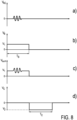
- Fig. 7 shows the operation of a CMUT device according to a first example
- Fig. 8 shows the operation of a CMUT device according to a second example.
- an alternating current or AC signal is supplied between the electrodes for transmitting ultrasound waves, for example using AC source 27 described above.
- the operating bias voltage V B is also supplied when the AC signal or voltage is supplied.
- the operating bias voltage V B is supplied during an operation phase of the CMUT device, i.e. during transmitting and/or receiving of ultrasound waves.
- the operating bias voltage V B can be supplied using the operating bias voltage source 25 described above.
- the operating bias voltage V B is supplied for a first time T B period during transmitting and/or receiving ultrasound waves, in particular using the control unit 40 described above.
- the AC signal or voltage V AC and the bias voltage V B during the operation phase of time period T B sum up to a sum voltage V sum , which is illustrated in Fig. 7c or Fig. 8c .
- the additional charging voltage Vc is not supplied during an operation phase, i.e. not during transmitting and/or receiving of ultrasound waves.
- the charging voltage V C can be supplied using the charging voltage source 30 described above.
- the charging voltage V C is supplied for a second time period T C during no transmitting and/or receiving of ultrasound waves, in particular using the control unit 40 described above.
- the second time period T C is before the first time period T B .
- first the additional charging voltage V C of the second polarity is supplied, and subsequently the operating bias voltage V B of the first, reverse polarity during the operation phase is supplied.
- the charging voltage can be supplied for a time period T C during manufacturing of the CMUT device such that it remains in the at least one dielectric layer 21, 23 substantially permanently, or it can be supplied when actually using the device using the control unit 40.
- the second time period T C is after the first time period T B .
- first the operating bias voltage V B of the first polarity during the operation phase is supplied, and subsequently the additional charging voltage Vc of the second, reverse polarity is supplied.
- the operating bias voltage V B is supplied at a first voltage level V1
- the charging voltage Vc is supplied at a second voltage level V2 different from the first voltage level V1.
- the voltage level V2 of the charging voltage Vc is not the same as the voltage level V1 of the operating bias voltage V B .
- the second voltage level V2 is smaller than the first voltage level V1.
- the second voltage level V2 is greater than the first voltage level V1.
- this may also be implemented the other way round.
- the voltage levels could also be the same.
- the second time period T C would be in between two first time periods T B .
- the charging voltage Vc can be supplied periodically, in particular before each scan line or before each frame. In this way, the device is intentionally charged in such a way as to increase output pressure and/or receive sensitivity during subsequent operation.
- the charging voltage Vc can be supplied can be supplied only once, for example during manufacturing, or only if needed, as for example determined by a monitoring unit which will be described in the following.
- Fig. 6 shows a schematic block diagram of a CMUT device including a feature present in all the embodiments of the present invention.
- the CMUT device 1 of Fig. 6 further comprises a monitoring unit 50 for monitoring the charge in the at least one dielectric layer 21, 23.
- the monitoring unit 50 is connected to the CMUT cell 10 via a connection 51.
- the monitoring unit can be implemented in the ASIC of the CMUT device as explained above.
- the control unit 40 and the monitoring unit 50 can be implemented in the same device, such as the ASIC of the CMUT device.
- the monitoring unit 50 is adapted to monitor a shift in a capacitance-versus-voltage curve of the CMUT device.
- the capacitance (between the electrodes 20, 22) can be measured via the connection 51 between the monitoring unit 50 and the CMUT cell 10
- the bias voltage V B can be measured via another connection (not shown in Fig. 6 ) between the monitoring unit 50 and the bias voltage source 25 or the control unit 40. In this way the capacitance-versus-voltage curve can be measured and then a shift can be monitored or detected therein.
- the monitoring unit 50 is adapted to monitor the output pressure and/or receive sensitivity while varying the charging voltage.
- the output pressure an/or receive sensitivity can be measured via the connection 51, and the charging voltage Vc can be varied via another connection (not shown in Fig. 6 ) between the monitoring unit 50 and the charging voltage source 30 or the control unit 40.
- a charging voltage can be determined that results in minimum acoustic pressure and/or sensitivity.
- the operating bias voltage and the charging voltage can be monitored, while also measuring the acoustic output pressure (e.g. by using a hydrophone). When the charging voltage is applied or supplied, it can be measured that the acoustic output pressure increases.
- the monitoring unit 50 is adapted to detect when the charge in the at least one dielectric layer is insufficient, in particular by comparing the currently monitored charge with a predefined value. For example, the currently measured shift in the capacitance-versus-voltage curve can be compared with a predefined value, or the currently measured output pressure and/or receive sensitivity can be compared with a predefined value.
- the control unit 40 is adapted to control the charging voltage source 30 to reapply the charging voltage when the monitoring unit 50 detects that the charge in the at least one dielectric layer is insufficient. For example, when the monitoring unit 50 detects insufficiency of charge a corresponding signal can be transmitted via connection 52 (indicated by dashed line in Fig. 6 ) between the monitoring unit 50 and the control unit 40.
- the charge in the dielectric layer(s) can be refreshed over the useful life of the CMUT device.
- This enables to sustain improved output pressure and/or receive sensitivity.
- the CMUT device can be in its normal operation until a time, when the output pressure and/or receive sensitivity has decreased and the CMUT device needs to be charged again with the charging voltage to achieve the desired output pressure and/or receive sensitivity.
- the CMUT device 1 described herein can be used in a variety of applications.
- the CMUT device 1 described herein can be used in a medical ultrasound system (e.g. diagnostic or therapeutic medical ultrasound system), in particular with ultrasound imaging functionality.
- the CMUT device 1 described herein can be a high-intensity focused ultrasound (HIFU) transducer device.
- HIFU high-intensity focused ultrasound
- a HIFU transducer device can for example be used in a medical system to heat and destroy pathogenic tissue rapidly through ablation.
- a high output pressure is required in a HIFU transducer device. Therefore the charging effect can be used in an optimal way for such a HIFU transducer device.
Applications Claiming Priority (2)
| Application Number | Priority Date | Filing Date | Title |
|---|---|---|---|
| US201261610130P | 2012-03-13 | 2012-03-13 | |
| PCT/IB2013/051631 WO2013136212A1 (en) | 2012-03-13 | 2013-03-01 | Capacitive micro-machined ultrasound transducer device with charging voltage source |
Publications (2)
| Publication Number | Publication Date |
|---|---|
| EP2825856A1 EP2825856A1 (en) | 2015-01-21 |
| EP2825856B1 true EP2825856B1 (en) | 2023-09-27 |
Family
ID=48142836
Family Applications (1)
| Application Number | Title | Priority Date | Filing Date |
|---|---|---|---|
| EP13717563.4A Active EP2825856B1 (en) | 2012-03-13 | 2013-03-01 | Capacitive micro-machined ultrasound transducer device with charging voltage source |
Country Status (5)
| Country | Link |
|---|---|
| US (1) | US9950342B2 (zh) |
| EP (1) | EP2825856B1 (zh) |
| JP (1) | JP6329491B2 (zh) |
| CN (1) | CN104160250B (zh) |
| WO (1) | WO2013136212A1 (zh) |
Families Citing this family (14)
| Publication number | Priority date | Publication date | Assignee | Title |
|---|---|---|---|---|
| JP6011235B2 (ja) * | 2012-10-17 | 2016-10-19 | セイコーエプソン株式会社 | 超音波測定装置、プローブヘッド、超音波プローブ、電子機器及び超音波診断装置 |
| JP6534190B2 (ja) * | 2013-09-27 | 2019-06-26 | コーニンクレッカ フィリップス エヌ ヴェKoninklijke Philips N.V. | 超音波トランスデューサアセンブリ並びに超音波を送信及び受信するための方法 |
| EP3223709B1 (en) * | 2014-11-25 | 2019-02-20 | Koninklijke Philips N.V. | Ultrasound system and method |
| US11766237B2 (en) | 2015-07-02 | 2023-09-26 | Philips Image Guided Therapy Corporation | Multi-mode capacitive micromachined ultrasound transducer and associated devices, systems, and methods for multiple different intravascular sensing capabilities |
| EP3334538A1 (en) | 2015-08-11 | 2018-06-20 | Koninklijke Philips N.V. | Capacitive micromachined ultrasonic transducers with increased lifetime |
| US9987661B2 (en) * | 2015-12-02 | 2018-06-05 | Butterfly Network, Inc. | Biasing of capacitive micromachined ultrasonic transducers (CMUTs) and related apparatus and methods |
| JP7208901B2 (ja) * | 2016-12-22 | 2023-01-19 | コーニンクレッカ フィリップス エヌ ヴェ | 容量性高周波微小電気機械スイッチのシステム及び動作方法 |
| US11864947B2 (en) | 2016-12-22 | 2024-01-09 | Koninklijke Philips N.V. | Systems and methods of operation of capacitive radio frequency micro-electromechanical switches |
| US11190868B2 (en) * | 2017-04-18 | 2021-11-30 | Massachusetts Institute Of Technology | Electrostatic acoustic transducer utilized in a headphone device or an earbud |
| US11026662B2 (en) * | 2018-01-11 | 2021-06-08 | Siemens Medical Solutions Usa, Inc. | Ultrasound transmit/receive for pulse inversion |
| FR3077162B1 (fr) * | 2018-01-22 | 2020-02-07 | Commissariat A L'energie Atomique Et Aux Energies Alternatives | Transducteur piezoelectrique |
| WO2021019296A1 (en) * | 2019-07-26 | 2021-02-04 | Vermon Sa | Cmut transducer and method for manufacturing |
| JP2021038981A (ja) * | 2019-09-02 | 2021-03-11 | 株式会社日立製作所 | 容量検出型超音波トランスデューサを使用した計測方法 |
| US11738369B2 (en) * | 2020-02-17 | 2023-08-29 | GE Precision Healthcare LLC | Capactive micromachined transducer having a high contact resistance part |
Family Cites Families (14)
| Publication number | Priority date | Publication date | Assignee | Title |
|---|---|---|---|---|
| US6443901B1 (en) | 2000-06-15 | 2002-09-03 | Koninklijke Philips Electronics N.V. | Capacitive micromachined ultrasonic transducers |
| JP4746291B2 (ja) | 2004-08-05 | 2011-08-10 | オリンパス株式会社 | 静電容量型超音波振動子、及びその製造方法 |
| JP4434109B2 (ja) * | 2005-09-05 | 2010-03-17 | 株式会社日立製作所 | 電気・音響変換素子 |
| JP4676988B2 (ja) * | 2005-09-05 | 2011-04-27 | 株式会社日立メディコ | 超音波撮像装置 |
| US8517948B2 (en) * | 2005-11-18 | 2013-08-27 | Hitachi Medical Corporation | Ultrasound diagnostic apparatus and method of calibrating the same |
| US7599254B2 (en) * | 2005-12-20 | 2009-10-06 | Siemens Medical Solutions Usa, Inc. | Transducer static discharge methods and apparatus |
| JP4852356B2 (ja) | 2006-06-27 | 2012-01-11 | 株式会社日立メディコ | 超音波診断装置 |
| JP4839176B2 (ja) | 2006-10-12 | 2011-12-21 | オリンパスメディカルシステムズ株式会社 | 超音波トランスデューサ及び超音波診断装置 |
| WO2008054395A1 (en) | 2006-11-03 | 2008-05-08 | Research Triangle Institute | Enhanced ultrasound imaging probes using flexure mode piezoelectric transducers |
| CN101873830B (zh) * | 2007-12-03 | 2013-03-20 | 科隆科技公司 | 双模式操作微机械超声换能器 |
| JP2009272824A (ja) * | 2008-05-02 | 2009-11-19 | Olympus Medical Systems Corp | 超音波振動子セル、超音波振動子および超音波内視鏡 |
| WO2010000020A1 (en) | 2008-06-30 | 2010-01-07 | Cathrx Ltd | A catheter |
| US8315125B2 (en) | 2009-03-18 | 2012-11-20 | Sonetics Ultrasound, Inc. | System and method for biasing CMUT elements |
| EP3079837B1 (en) * | 2013-12-12 | 2023-02-08 | Koninklijke Philips N.V. | Monolithically integrated three electrode cmut device |
-
2013
- 2013-03-01 CN CN201380013597.7A patent/CN104160250B/zh active Active
- 2013-03-01 WO PCT/IB2013/051631 patent/WO2013136212A1/en active Application Filing
- 2013-03-01 EP EP13717563.4A patent/EP2825856B1/en active Active
- 2013-03-01 US US14/382,560 patent/US9950342B2/en active Active
- 2013-03-01 JP JP2014561548A patent/JP6329491B2/ja active Active
Non-Patent Citations (1)
| Title |
|---|
| S.H. WONG ET AL: "Capacitive Micromachined Ultrasonic Transducers for Therapeutic Ultrasound Applications", IEEE TRANSACTIONS ON BIOMEDICAL ENGINEERING., vol. 57, no. 1, 1 January 2010 (2010-01-01), PISCATAWAY, NJ, USA., pages 114 - 123, XP055556437, ISSN: 0018-9294, DOI: 10.1109/TBME.2009.2026909 * |
Also Published As
| Publication number | Publication date |
|---|---|
| CN104160250A (zh) | 2014-11-19 |
| US20150016227A1 (en) | 2015-01-15 |
| US9950342B2 (en) | 2018-04-24 |
| WO2013136212A1 (en) | 2013-09-19 |
| JP6329491B2 (ja) | 2018-05-23 |
| EP2825856A1 (en) | 2015-01-21 |
| JP2015513272A (ja) | 2015-04-30 |
| CN104160250B (zh) | 2017-10-27 |
Similar Documents
| Publication | Publication Date | Title |
|---|---|---|
| EP2825856B1 (en) | Capacitive micro-machined ultrasound transducer device with charging voltage source | |
| US7728487B2 (en) | Ultrasound transducer manufactured by using micromachining process, its device, endoscopic ultrasound diagnosis system thereof, and method for controlling the same | |
| US5677965A (en) | Integrated capacitive transducer | |
| US6707236B2 (en) | Non-contact electroactive polymer electrodes | |
| RU2511671C2 (ru) | Емкостной микрообработанный ультразвуковой преобразователь | |
| US10101303B2 (en) | Capacitive micromachined ultrasonic transducer and test object information acquiring apparatus including capacitive micromachined ultrasonic transducer | |
| KR101689346B1 (ko) | 기계적 붕괴 보유를 갖는 사전 붕괴된 cmut | |
| JP5473579B2 (ja) | 静電容量型電気機械変換装置の制御装置、及び静電容量型電気機械変換装置の制御方法 | |
| JP5408937B2 (ja) | 電気機械変換素子及びその製造方法 | |
| US20100244623A1 (en) | Capacitive Micromachined Ultrasonic Transducer with Voltage Feedback | |
| JP4523879B2 (ja) | 電気・音響変換素子、アレイ型超音波トランスデューサおよび超音波診断装置 | |
| US8035949B2 (en) | Semiconductor device and method of controlling electrostatic actuator | |
| KR101630759B1 (ko) | 초음파 변환기의 셀, 채널 및 이를 포함하는 초음파 변환기 | |
| US20160144402A1 (en) | Capacitive transducer and sample information acquisition apparatus | |
| JP4958631B2 (ja) | 超音波送受信デバイス及びそれを用いた超音波探触子 | |
| US10016788B2 (en) | Method and device for driving capacitance transducer | |
| JP2009272824A (ja) | 超音波振動子セル、超音波振動子および超音波内視鏡 | |
| US10743840B2 (en) | Ultrasound transducer assembly and method for transmitting and receiving ultrasound waves | |
| WO2014038238A1 (ja) | 超音波ユニット及び超音波内視鏡 | |
| US20220021990A1 (en) | Vibration module for placement on an eardrum | |
| JP6071286B2 (ja) | 静電容量型トランスデューサ及びその製造方法 | |
| JP6286000B2 (ja) | 静電容量型トランスデューサの駆動方法および駆動装置 | |
| JP2011211059A (ja) | 超音波発生器、超音波発生器の駆動方法及び超音波センサ | |
| JP2019209169A (ja) | 静電容量型トランスデューサ、及び被検体情報取得装置 | |
| US20150108871A1 (en) | Ultrasonic transducer with dielectric elastomer as active layer |
Legal Events
| Date | Code | Title | Description |
|---|---|---|---|
| PUAI | Public reference made under article 153(3) epc to a published international application that has entered the european phase |
Free format text: ORIGINAL CODE: 0009012 |
|
| 17P | Request for examination filed |
Effective date: 20141013 |
|
| AK | Designated contracting states |
Kind code of ref document: A1 Designated state(s): AL AT BE BG CH CY CZ DE DK EE ES FI FR GB GR HR HU IE IS IT LI LT LU LV MC MK MT NL NO PL PT RO RS SE SI SK SM TR |
|
| AX | Request for extension of the european patent |
Extension state: BA ME |
|
| DAX | Request for extension of the european patent (deleted) | ||
| STAA | Information on the status of an ep patent application or granted ep patent |
Free format text: STATUS: EXAMINATION IS IN PROGRESS |
|
| 17Q | First examination report despatched |
Effective date: 20190221 |
|
| RAP1 | Party data changed (applicant data changed or rights of an application transferred) |
Owner name: KONINKLIJKE PHILIPS N.V. |
|
| STAA | Information on the status of an ep patent application or granted ep patent |
Free format text: STATUS: EXAMINATION IS IN PROGRESS |
|
| STAA | Information on the status of an ep patent application or granted ep patent |
Free format text: STATUS: EXAMINATION IS IN PROGRESS |
|
| REG | Reference to a national code |
Ref country code: DE Ref legal event code: R079 Ref document number: 602013084703 Country of ref document: DE Free format text: PREVIOUS MAIN CLASS: G01H0011060000 Ipc: B06B0001020000 Ref country code: DE Ref legal event code: R079 Free format text: PREVIOUS MAIN CLASS: G01H0011060000 Ipc: B06B0001020000 |
|
| GRAP | Despatch of communication of intention to grant a patent |
Free format text: ORIGINAL CODE: EPIDOSNIGR1 |
|
| STAA | Information on the status of an ep patent application or granted ep patent |
Free format text: STATUS: GRANT OF PATENT IS INTENDED |
|
| RIC1 | Information provided on ipc code assigned before grant |
Ipc: G01N 29/24 20060101ALI20230411BHEP Ipc: B06B 1/02 20060101AFI20230411BHEP |
|
| INTG | Intention to grant announced |
Effective date: 20230425 |
|
| GRAS | Grant fee paid |
Free format text: ORIGINAL CODE: EPIDOSNIGR3 |
|
| GRAA | (expected) grant |
Free format text: ORIGINAL CODE: 0009210 |
|
| STAA | Information on the status of an ep patent application or granted ep patent |
Free format text: STATUS: THE PATENT HAS BEEN GRANTED |
|
| AK | Designated contracting states |
Kind code of ref document: B1 Designated state(s): AL AT BE BG CH CY CZ DE DK EE ES FI FR GB GR HR HU IE IS IT LI LT LU LV MC MK MT NL NO PL PT RO RS SE SI SK SM TR |
|
| REG | Reference to a national code |
Ref country code: GB Ref legal event code: FG4D |
|
| REG | Reference to a national code |
Ref country code: CH Ref legal event code: EP |
|
| REG | Reference to a national code |
Ref country code: DE Ref legal event code: R096 Ref document number: 602013084703 Country of ref document: DE |
|
| REG | Reference to a national code |
Ref country code: DE Ref legal event code: R084 Ref document number: 602013084703 Country of ref document: DE |
|
| REG | Reference to a national code |
Ref country code: IE Ref legal event code: FG4D |
|
| REG | Reference to a national code |
Ref country code: GB Ref legal event code: 746 Effective date: 20231031 |
|
| REG | Reference to a national code |
Ref country code: LT Ref legal event code: MG9D |
|
| PG25 | Lapsed in a contracting state [announced via postgrant information from national office to epo] |
Ref country code: GR Free format text: LAPSE BECAUSE OF FAILURE TO SUBMIT A TRANSLATION OF THE DESCRIPTION OR TO PAY THE FEE WITHIN THE PRESCRIBED TIME-LIMIT Effective date: 20231228 |
|
| PG25 | Lapsed in a contracting state [announced via postgrant information from national office to epo] |
Ref country code: SE Free format text: LAPSE BECAUSE OF FAILURE TO SUBMIT A TRANSLATION OF THE DESCRIPTION OR TO PAY THE FEE WITHIN THE PRESCRIBED TIME-LIMIT Effective date: 20230927 Ref country code: RS Free format text: LAPSE BECAUSE OF FAILURE TO SUBMIT A TRANSLATION OF THE DESCRIPTION OR TO PAY THE FEE WITHIN THE PRESCRIBED TIME-LIMIT Effective date: 20230927 Ref country code: NO Free format text: LAPSE BECAUSE OF FAILURE TO SUBMIT A TRANSLATION OF THE DESCRIPTION OR TO PAY THE FEE WITHIN THE PRESCRIBED TIME-LIMIT Effective date: 20231227 Ref country code: LV Free format text: LAPSE BECAUSE OF FAILURE TO SUBMIT A TRANSLATION OF THE DESCRIPTION OR TO PAY THE FEE WITHIN THE PRESCRIBED TIME-LIMIT Effective date: 20230927 Ref country code: LT Free format text: LAPSE BECAUSE OF FAILURE TO SUBMIT A TRANSLATION OF THE DESCRIPTION OR TO PAY THE FEE WITHIN THE PRESCRIBED TIME-LIMIT Effective date: 20230927 Ref country code: HR Free format text: LAPSE BECAUSE OF FAILURE TO SUBMIT A TRANSLATION OF THE DESCRIPTION OR TO PAY THE FEE WITHIN THE PRESCRIBED TIME-LIMIT Effective date: 20230927 Ref country code: GR Free format text: LAPSE BECAUSE OF FAILURE TO SUBMIT A TRANSLATION OF THE DESCRIPTION OR TO PAY THE FEE WITHIN THE PRESCRIBED TIME-LIMIT Effective date: 20231228 Ref country code: FI Free format text: LAPSE BECAUSE OF FAILURE TO SUBMIT A TRANSLATION OF THE DESCRIPTION OR TO PAY THE FEE WITHIN THE PRESCRIBED TIME-LIMIT Effective date: 20230927 |
|
| REG | Reference to a national code |
Ref country code: NL Ref legal event code: MP Effective date: 20230927 |
|
| REG | Reference to a national code |
Ref country code: AT Ref legal event code: MK05 Ref document number: 1614878 Country of ref document: AT Kind code of ref document: T Effective date: 20230927 |
|
| PG25 | Lapsed in a contracting state [announced via postgrant information from national office to epo] |
Ref country code: NL Free format text: LAPSE BECAUSE OF FAILURE TO SUBMIT A TRANSLATION OF THE DESCRIPTION OR TO PAY THE FEE WITHIN THE PRESCRIBED TIME-LIMIT Effective date: 20230927 |
|
| PG25 | Lapsed in a contracting state [announced via postgrant information from national office to epo] |
Ref country code: IS Free format text: LAPSE BECAUSE OF FAILURE TO SUBMIT A TRANSLATION OF THE DESCRIPTION OR TO PAY THE FEE WITHIN THE PRESCRIBED TIME-LIMIT Effective date: 20240127 |
|
| PG25 | Lapsed in a contracting state [announced via postgrant information from national office to epo] |
Ref country code: AT Free format text: LAPSE BECAUSE OF FAILURE TO SUBMIT A TRANSLATION OF THE DESCRIPTION OR TO PAY THE FEE WITHIN THE PRESCRIBED TIME-LIMIT Effective date: 20230927 |
|
| PG25 | Lapsed in a contracting state [announced via postgrant information from national office to epo] |
Ref country code: ES Free format text: LAPSE BECAUSE OF FAILURE TO SUBMIT A TRANSLATION OF THE DESCRIPTION OR TO PAY THE FEE WITHIN THE PRESCRIBED TIME-LIMIT Effective date: 20230927 |
|
| PG25 | Lapsed in a contracting state [announced via postgrant information from national office to epo] |
Ref country code: SM Free format text: LAPSE BECAUSE OF FAILURE TO SUBMIT A TRANSLATION OF THE DESCRIPTION OR TO PAY THE FEE WITHIN THE PRESCRIBED TIME-LIMIT Effective date: 20230927 Ref country code: RO Free format text: LAPSE BECAUSE OF FAILURE TO SUBMIT A TRANSLATION OF THE DESCRIPTION OR TO PAY THE FEE WITHIN THE PRESCRIBED TIME-LIMIT Effective date: 20230927 Ref country code: IS Free format text: LAPSE BECAUSE OF FAILURE TO SUBMIT A TRANSLATION OF THE DESCRIPTION OR TO PAY THE FEE WITHIN THE PRESCRIBED TIME-LIMIT Effective date: 20240127 Ref country code: ES Free format text: LAPSE BECAUSE OF FAILURE TO SUBMIT A TRANSLATION OF THE DESCRIPTION OR TO PAY THE FEE WITHIN THE PRESCRIBED TIME-LIMIT Effective date: 20230927 Ref country code: EE Free format text: LAPSE BECAUSE OF FAILURE TO SUBMIT A TRANSLATION OF THE DESCRIPTION OR TO PAY THE FEE WITHIN THE PRESCRIBED TIME-LIMIT Effective date: 20230927 Ref country code: CZ Free format text: LAPSE BECAUSE OF FAILURE TO SUBMIT A TRANSLATION OF THE DESCRIPTION OR TO PAY THE FEE WITHIN THE PRESCRIBED TIME-LIMIT Effective date: 20230927 Ref country code: AT Free format text: LAPSE BECAUSE OF FAILURE TO SUBMIT A TRANSLATION OF THE DESCRIPTION OR TO PAY THE FEE WITHIN THE PRESCRIBED TIME-LIMIT Effective date: 20230927 Ref country code: SK Free format text: LAPSE BECAUSE OF FAILURE TO SUBMIT A TRANSLATION OF THE DESCRIPTION OR TO PAY THE FEE WITHIN THE PRESCRIBED TIME-LIMIT Effective date: 20230927 Ref country code: PT Free format text: LAPSE BECAUSE OF FAILURE TO SUBMIT A TRANSLATION OF THE DESCRIPTION OR TO PAY THE FEE WITHIN THE PRESCRIBED TIME-LIMIT Effective date: 20240129 |
|
| PGFP | Annual fee paid to national office [announced via postgrant information from national office to epo] |
Ref country code: DE Payment date: 20240328 Year of fee payment: 12 Ref country code: GB Payment date: 20240319 Year of fee payment: 12 |