EP2823507B1 - Verfahren zum bilden eines kontakts auf einem halbleitersubstrat und halbleitervorrichtung - Google Patents
Verfahren zum bilden eines kontakts auf einem halbleitersubstrat und halbleitervorrichtung Download PDFInfo
- Publication number
- EP2823507B1 EP2823507B1 EP13702433.7A EP13702433A EP2823507B1 EP 2823507 B1 EP2823507 B1 EP 2823507B1 EP 13702433 A EP13702433 A EP 13702433A EP 2823507 B1 EP2823507 B1 EP 2823507B1
- Authority
- EP
- European Patent Office
- Prior art keywords
- semiconductor substrate
- metal
- contact
- layer
- insulating layer
- Prior art date
- Legal status (The legal status is an assumption and is not a legal conclusion. Google has not performed a legal analysis and makes no representation as to the accuracy of the status listed.)
- Active
Links
Images
Classifications
-
- H—ELECTRICITY
- H10—SEMICONDUCTOR DEVICES; ELECTRIC SOLID-STATE DEVICES NOT OTHERWISE PROVIDED FOR
- H10D—INORGANIC ELECTRIC SEMICONDUCTOR DEVICES
- H10D64/00—Electrodes of devices having potential barriers
- H10D64/20—Electrodes characterised by their shapes, relative sizes or dispositions
- H10D64/23—Electrodes carrying the current to be rectified, amplified, oscillated or switched, e.g. sources, drains, anodes or cathodes
- H10D64/251—Source or drain electrodes for field-effect devices
- H10D64/258—Source or drain electrodes for field-effect devices characterised by the relative positions of the source or drain electrodes with respect to the gate electrode
-
- H—ELECTRICITY
- H10—SEMICONDUCTOR DEVICES; ELECTRIC SOLID-STATE DEVICES NOT OTHERWISE PROVIDED FOR
- H10D—INORGANIC ELECTRIC SEMICONDUCTOR DEVICES
- H10D12/00—Bipolar devices controlled by the field effect, e.g. insulated-gate bipolar transistors [IGBT]
- H10D12/01—Manufacture or treatment
- H10D12/031—Manufacture or treatment of IGBTs
-
- H—ELECTRICITY
- H10—SEMICONDUCTOR DEVICES; ELECTRIC SOLID-STATE DEVICES NOT OTHERWISE PROVIDED FOR
- H10D—INORGANIC ELECTRIC SEMICONDUCTOR DEVICES
- H10D30/00—Field-effect transistors [FET]
- H10D30/01—Manufacture or treatment
- H10D30/021—Manufacture or treatment of FETs having insulated gates [IGFET]
- H10D30/028—Manufacture or treatment of FETs having insulated gates [IGFET] of double-diffused metal oxide semiconductor [DMOS] FETs
- H10D30/0291—Manufacture or treatment of FETs having insulated gates [IGFET] of double-diffused metal oxide semiconductor [DMOS] FETs of vertical DMOS [VDMOS] FETs
-
- H—ELECTRICITY
- H10—SEMICONDUCTOR DEVICES; ELECTRIC SOLID-STATE DEVICES NOT OTHERWISE PROVIDED FOR
- H10D—INORGANIC ELECTRIC SEMICONDUCTOR DEVICES
- H10D30/00—Field-effect transistors [FET]
- H10D30/60—Insulated-gate field-effect transistors [IGFET]
-
- H—ELECTRICITY
- H10—SEMICONDUCTOR DEVICES; ELECTRIC SOLID-STATE DEVICES NOT OTHERWISE PROVIDED FOR
- H10D—INORGANIC ELECTRIC SEMICONDUCTOR DEVICES
- H10D62/00—Semiconductor bodies, or regions thereof, of devices having potential barriers
- H10D62/80—Semiconductor bodies, or regions thereof, of devices having potential barriers characterised by the materials
- H10D62/83—Semiconductor bodies, or regions thereof, of devices having potential barriers characterised by the materials being Group IV materials, e.g. B-doped Si or undoped Ge
- H10D62/832—Semiconductor bodies, or regions thereof, of devices having potential barriers characterised by the materials being Group IV materials, e.g. B-doped Si or undoped Ge being Group IV materials comprising two or more elements, e.g. SiGe
- H10D62/8325—Silicon carbide
-
- H—ELECTRICITY
- H10—SEMICONDUCTOR DEVICES; ELECTRIC SOLID-STATE DEVICES NOT OTHERWISE PROVIDED FOR
- H10D—INORGANIC ELECTRIC SEMICONDUCTOR DEVICES
- H10D64/00—Electrodes of devices having potential barriers
- H10D64/01—Manufacture or treatment
- H10D64/011—Manufacture or treatment of electrodes ohmically coupled to a semiconductor
- H10D64/0111—Manufacture or treatment of electrodes ohmically coupled to a semiconductor to Group IV semiconductors
- H10D64/0112—Manufacture or treatment of electrodes ohmically coupled to a semiconductor to Group IV semiconductors using conductive layers comprising silicides
-
- H—ELECTRICITY
- H10—SEMICONDUCTOR DEVICES; ELECTRIC SOLID-STATE DEVICES NOT OTHERWISE PROVIDED FOR
- H10D—INORGANIC ELECTRIC SEMICONDUCTOR DEVICES
- H10D64/00—Electrodes of devices having potential barriers
- H10D64/01—Manufacture or treatment
- H10D64/011—Manufacture or treatment of electrodes ohmically coupled to a semiconductor
- H10D64/0111—Manufacture or treatment of electrodes ohmically coupled to a semiconductor to Group IV semiconductors
- H10D64/0115—Manufacture or treatment of electrodes ohmically coupled to a semiconductor to Group IV semiconductors to silicon carbide
-
- H—ELECTRICITY
- H10—SEMICONDUCTOR DEVICES; ELECTRIC SOLID-STATE DEVICES NOT OTHERWISE PROVIDED FOR
- H10D—INORGANIC ELECTRIC SEMICONDUCTOR DEVICES
- H10D64/00—Electrodes of devices having potential barriers
- H10D64/60—Electrodes characterised by their materials
- H10D64/62—Electrodes ohmically coupled to a semiconductor
-
- H—ELECTRICITY
- H10—SEMICONDUCTOR DEVICES; ELECTRIC SOLID-STATE DEVICES NOT OTHERWISE PROVIDED FOR
- H10P—GENERIC PROCESSES OR APPARATUS FOR THE MANUFACTURE OR TREATMENT OF DEVICES COVERED BY CLASS H10
- H10P14/00—Formation of materials, e.g. in the shape of layers or pillars
- H10P14/40—Formation of materials, e.g. in the shape of layers or pillars of conductive or resistive materials
- H10P14/412—Deposition of metallic or metal-silicide materials
-
- H—ELECTRICITY
- H10—SEMICONDUCTOR DEVICES; ELECTRIC SOLID-STATE DEVICES NOT OTHERWISE PROVIDED FOR
- H10P—GENERIC PROCESSES OR APPARATUS FOR THE MANUFACTURE OR TREATMENT OF DEVICES COVERED BY CLASS H10
- H10P50/00—Etching of wafers, substrates or parts of devices
- H10P50/20—Dry etching; Plasma etching; Reactive-ion etching
- H10P50/26—Dry etching; Plasma etching; Reactive-ion etching of conductive or resistive materials
- H10P50/264—Dry etching; Plasma etching; Reactive-ion etching of conductive or resistive materials by chemical means
- H10P50/266—Dry etching; Plasma etching; Reactive-ion etching of conductive or resistive materials by chemical means by vapour etching only
-
- H—ELECTRICITY
- H10—SEMICONDUCTOR DEVICES; ELECTRIC SOLID-STATE DEVICES NOT OTHERWISE PROVIDED FOR
- H10P—GENERIC PROCESSES OR APPARATUS FOR THE MANUFACTURE OR TREATMENT OF DEVICES COVERED BY CLASS H10
- H10P95/00—Generic processes or apparatus for manufacture or treatments not covered by the other groups of this subclass
Definitions
- the invention relates to a method for forming a contact on a semiconductor substrate.
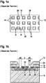
- FIG. 1a and 1b show schematic representations of a semiconductor device according to the prior art.
- the semiconductor device comprises a silicon carbide carrier 10, on the upper side of which a gate stack structure 12 and a multiplicity of conductive contacts 14 are formed.
- the gate stack structure 12 comprises a gate oxide layer 16 applied to the upper side of the silicon carbide carrier 10, a gate metallization layer 18 at least partially covering the gate oxide layer 16 and an insulating layer 20 applied to the layers 16 and 18 by means of the implants 22 to 26 in different concentrations, each of the contacts 14 is electrically connected to the gate stack structure 12. In addition, each of the contacts 14 is arranged in an opening 28 in the gate stack structure 12.
- the wet or dry chemical structuring of the contacts 14 in the openings 28 is possible according to the prior art by maintaining a distance a0 between an edge of each opening 28 and an edge of a lithography mask (not shown).
- the distance a0 is at least over 20 nm, mostly over 50 nm, usually over 100 nm.
- the distance a0 is comparatively large to an extension b of each contact 14 oriented parallel to the upper side of the silicon carbide carrier 10.
- WO 2010/095544 A1 a method of manufacturing a semiconductor device.
- a metal film is deposited on the surfaces of the subsequent contacts and on an insulating layer framing the surfaces and then heated to a temperature between 300 ° C and 800 ° C. Then residues of the metal film are removed by means of a chemical etching step.
- the invention provides a method for forming a contact on a semiconductor substrate with the features of claim 1.
- quasi-self-aligned contacts can be produced without their own lithography level.
- they can also be structured with a lithography level with low requirements for the adjustment and low requirements for the etching reserve.
- a rough structuring of the at least one metal can be carried out prior to the heating of the semiconductor substrate take place, whereby it can be prevented that the at least one metal reacts at undesired locations with the material of the semiconductor substrate or at least one substance applied thereon during the heating.
- the method for producing the advantageous semiconductor device can be used.
- the method can thus be used to implement a relatively small distance of less than 10 nm between a gate stack structure and at least one contact. Due to the fact that a significantly reduced distance can be formed between the at least one contact and the gate stack structure, the semiconductor device can be realized with a smaller dimension parallel to the substrate surface provided with at least one contact.
- the material saving obtained in this way such as, for example, saving the substrate material, means that the advantageous semiconductor device can be produced more cheaply.
- the smaller formability of the semiconductor device makes it easier to transport, attach, and use.
- the realization of a smaller distance between the at least one gate stack structure and the at least one contact can also be achieved for a higher cell concentration on an area of the surface Contacts equipped substrate surface can be used.
- the present invention can also be used to reduce a forward resistance of a transistor.
- At least one of the contacts is formed at a distance from at least one gate stack structure that is smaller than 10 nm, the gate stack structure being a gate oxide layer deposited on the semiconductor substrate, a gate oxide layer partially covering the gate oxide layer Gate metallization layer and the insulating layer applied to the gate stack structure and the gate metallization layer.
- the gate stack structure being a gate oxide layer deposited on the semiconductor substrate, a gate oxide layer partially covering the gate oxide layer Gate metallization layer and the insulating layer applied to the gate stack structure and the gate metallization layer.
- nickel, titanium, aluminum, tantalum and / or tungsten can be applied as the at least one metal.
- the advantageous method is therefore suitable for forming a large number of contacts from different materials.
- the insulating layer can be formed on at least one partial outside of the outside of the semiconductor substrate and / or the layer applied to the semiconductor substrate and the at least one partial area of the outside of the semiconductor substrate and / or the layer applied to the semiconductor substrate on at least one Location of the at least one contact to be formed.
- at least one silicon oxide layer and / or one silicon nitride layer can be formed as the insulating layer. In this way, inexpensive and simple processable materials can be used for the insulating layer.
- a gate oxide layer deposited on the semiconductor substrate and a gate metallization layer partially covering the gate oxide layer can be covered by the insulating layer.
- the covered component can be reliably protected from contact with the at least one metal during the heating of the semiconductor substrate.
- the insulating layer covering a gate stack substructure can be used to complete the gate stack structure as a subunit thereof. This multifunctionality of the insulating layer means that process steps and materials can be saved.
- the substrate can be heated to a temperature of at least 600 ° C. during the heating. Such a process step can be carried out simply and quickly by means of an oven.
- an isotopic etching step is carried out as the etching step using the etching material with the higher etching rate for the at least one metal than for the semiconductor metal material.
- the etching step is thus simple and can be carried out within a comparatively short time.
- At least one source contact is formed as the at least one contact. This is advantageous since, in particular in the case of a MOSFET, a smaller distance between each source contact and an adjacent gate stack structure is desired.
- the feasibility of the method described here is not limited to the production of source contacts.
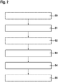
- FIG. 12 shows a flowchart for illustrating a method for forming a contact on a semiconductor substrate, which does not fall under the present invention.
- structures interacting with the at least one contact formed can later be formed on the semiconductor substrate.
- at least one implantation can be introduced in the semiconductor substrate.
- at least one material can be deposited on the semiconductor substrate.
- at least one gate stack structure and / or at least one gate stack substructure can be formed on the semiconductor substrate.
- a gate oxidation can be carried out and / or a gate metallization, such as polysilicon, can be deposited.
- an insulating layer can be applied in method step S0 on at least one partial outside of the outside of the semiconductor substrate and / or on the
- the insulating layer can comprise a high-temperature oxide which is formed at a temperature between 600 ° C and 1000 ° C.
- DCS and nitrogen oxide (N 2 O) can be used as raw materials for forming the insulating layer.
- other materials can also be used to form the insulating layer.
- At least one gate stack structure and / or at least one gate stack substructure can be covered by the insulating layer. If at least one gate stack substructure is covered by the insulating layer, at least regions of the insulating layer can also be used as a subunit of the gate stack structure formed thereby. This multifunctionality of the insulating layer means that materials and / or process steps can be saved.
- step S0 at least one partial area of the outside of the semiconductor substrate and / or of the layer applied to the semiconductor substrate can also be exposed by the previously formed insulating layer at at least one point of the at least one contact to be formed.
- Conventional structuring steps can be carried out for structuring the insulating layer.
- a method step S1 at least one metal is applied to at least one exposed partial area of the outside of the semiconductor substrate and / or the layer applied to the semiconductor substrate.
- at least one edge region of the insulating layer, which frames the (previously exposed) partial area is at least partially covered with the at least one metal.
- the at least one metal can thus be applied comparatively over a large area.
- nickel, titanium, aluminum, tantalum and / or tungsten can be applied as the at least one metal.
- this can be sputtered onto the unmasked semiconductor substrate in particular.
- Method step S1 can thus be carried out simply and quickly.
- the at least one applied metal can be roughly structured. For example, this can be done by means of a lithography step and a wet chemical etching. It should be noted that the Method step S2 is not necessary for executing the method. This structuring step can be dispensed with in particular if all the structures to be protected on the outside from a reaction with the at least one metal are covered by the insulating layer. If method step S2 is carried out, a rough structuring of the at least one metal is sufficient. In particular, it is pointed out that it is not necessary to expose the at least one edge region of the insulating layer from the at least one metal.
- the semiconductor substrate is heated with the at least one metal applied to the at least one partial area and the at least one edge region.
- the heating stimulates a reaction of the at least one metal applied to the at least one partial area with at least one semiconductor material of the at least one partial area to form a semiconductor-metal material (as end material or further processing material of at least one contact).
- the semiconductor substrate can be heated to a temperature of at least 600 ° C.
- the semiconductor substrate is heated to a temperature around 1000 ° C. for a period of about 2 minutes.
- the temperature to be maintained during the heating and the duration of this method step can be chosen relatively freely, taking into account the at least one applied metal and / or the semiconductor material of the at least one partial area.
- the semiconductor substrate with the at least one metal applied to the at least one partial surface and the at least one edge region can be heated, for example, by a rapid thermal anneal process step.
- the at least one metal and the at least one semiconductor material can react to the end material of the later at least one contact during the heating.
- a further processing material can also arise, for which the at least one metal and the at least one semiconductor material react with one another, which in a further process step (not described) reacts with at least one other substance to form the end material of the at least one contact.
- the ohmic behavior of the at least one contact formed at this time or later can also be formed by the heating. If desired, one can be used to form the ohmic behavior sufficiently high temperature can be set during heating. An alternative approach to this is described below.
- the at least one metal can partially react with the insulating layer.
- the consumption of the insulating material of the insulating layer is generally negligible. If the insulating layer is still to perform a function even after the at least one contact has been formed, the consumption can be easily compensated for by forming the insulating layer with a slightly increased thickness, for example by 40 nm.
- an etching step is carried out as step S4. This is done using an etching material with a higher etching rate for the at least one metal than for the semiconductor metal material.
- the etching step carried out in method step S4 can in particular be an isotopic etching step. It is pointed out that a large number of etching materials can be used to carry out method step S4.
- the selection of the etching material can be chosen relatively freely, taking into account the at least one metal and the semiconductor metal material. For example, the nickel used as the at least one metal can be easily removed in process step S4 with a mixture of phosphoric and nitric acids. Residual traces of the at least one metal can remain on an outer surface of the insulating layer. These residual traces can in particular also be bonds made from the at least one metal and the insulating material of the insulating layer.
- the semiconductor substrate produced by means of the method steps described above can be processed further using known methods.
- the at least one contact formed by means of the method described above can be formed at a distance from at least one gate stack structure which is aligned parallel to the semiconductor surface equipped with the at least one contact and which is less than 10 nm. In particular, the distance can be less than 5 nm.
- the method described above can thus be used to arrange the at least one contact formed on at least one gate stack structure which ensures an advantageous high cell density on the semiconductor surface.
- At least one source contact is formed as the at least one contact.
- the source contact can be formed on a silicon carbide substrate, for example.
- the method can thus be used to form a power semiconductor (MOSFET) without a structuring step for structuring the source contact.
- MOSFET power semiconductor
- the usability of the method described here is not limited to a power semiconductor with source contacts. Instead, a large number of electrical components can be produced using the method described here.
- the at least one deposited metal is heated to a comparatively lower temperature between 500 ° C. and 800 ° C. in a first furnace process during method step S3.
- This first furnace process allows the at least one metal to react with the semiconductor material, such as silicon carbide, for example, without the reaction product becoming ohmic / highly conductive.
- the low temperature can reduce the probability of a reaction between the at least one metal and the insulating material of the insulating layer.
- the remaining at least one metal can then be removed in method step S4.
- a second furnace process can then be carried out as an optional method step S5 in order to ensure a sufficiently good conductivity of the at least one contact by means of a higher temperature.
- the advantage of this procedure is a lower degradation of the insulating material of the insulating layer during process step S3 while maintaining the low contact resistances.
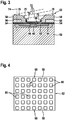
- Fig. 3 shows a schematic cross section through a semiconductor substrate for explaining an embodiment of the method for forming a contact on a semiconductor substrate.
- FIG. 3 A semiconductor substrate 50 with a gate stack structure 52 formed thereon is shown schematically.
- the semiconductor substrate 50 can be, for example Silicon carbide substrate.
- the feasibility of the method described below is not limited to the use of a silicon carbide substrate as the semiconductor substrate 50.
- a gate oxide layer 54 is deposited on the semiconductor substrate 50 to form the gate stack structure 52.
- the gate oxide layer 54 is partially covered by a gate metallization layer 56, for example made of polysilicon.
- An insulating layer 58 such as a silicon oxide layer and / or silicon oxide layer, is applied to the gate layers 54 and 56.
- the formation of the gate stack structure 52 from the layers 54 to 58 can only be interpreted as an example.
- implantations 60 to 64 can also be introduced into the semiconductor substrate 50, by means of which an electrical connection between the gate stack structure 52 and a contact formed by means of the method described below can be formed.
- concentrations and ions of the implantations 60 to 64 can be selected with great design freedom.
- the method has the method step S1 already described above, in which at least one metal, such as nickel, titanium, aluminum, tantalum and / or tungsten, is deposited. In this way, at least one partial surface 68 / opening (still) exposed or exposed by the layers 54 to 58 is covered with the at least one metal 66.
- the at least one metal 66 can be applied over such a large area that at least one edge region 70 of the insulating layer 58, which frames the at least one partial surface 68, is at least partially covered with the at least one metal 66.
- Method step S2 already described above can then optionally be carried out.
- an ion beam etching step is carried out in an etching direction 72 which is inclined to one perpendicular to an outside of the semiconductor substrate 50 with the axis 74 / wafer perpendicular aligned with the semiconductor structure 52 formed thereon.
- the etching direction 72 can be inclined to the axis 74 / wafer perpendicular by an angle between 5 ° to 88 °, preferably between 30 ° to 85 °, preferably between 60 ° to 80 °.
- the Executability of the in Fig. 3 Process step shown is not limited to a certain angle.
- the at least one metal 66 can be removed from the gate stack structure 52 in a simple manner over a large area.
- the at least one metal 66 is only removed during the ion beam etching / ion beam etching step from at least one upper side 76 of the gate stack structure 52 facing away from the semiconductor substrate 50 and at least one side wall region 78 of the gate stack structure 52 lying adjacent to the upper side 76.
- the gate stack structure 52 functions as a shield, which is why the at least one metal 66 is not / hardly removed from the partial area 68 and the edge area 70 of the insulating layer 58. This can be described as meaning that the at least one metal 66 is not or only partially removed from the at least one partial area 68, which can be designated as the bottom of an opening in the gate stack structure 52, and the at least one adjacent edge area 70.
- the at least one metal 66 can be removed from the at least one top side 76 and the at least one adjacent side wall region 78 of the gate stack structure 52 before the method step S3 / the contact alloy. This has the effect that (almost) no residual traces of the at least one metal 66 remain on the insulating layer 52 after the method steps S3 and S4 listed below. In this way, improved adhesion of the bond metallization and increased reliability of the semiconductor device produced by the method can be ensured.
- Fig. 4 shows a schematic plan view of a semiconductor device which does not fall under the present invention.
- semiconductor device shown schematically comprises a (not shown) semiconductor substrate and at least one on and / or in at least one Partial surface 68 of an outside of the semiconductor substrate and / or a contact 80 arranged on the semiconductor substrate, which contact is formed from a semiconductor metal material.
- the semiconductor device has a gate stack structure 52 on the outside of the semiconductor substrate and / or a layer applied to the semiconductor substrate, which is arranged adjacent to the at least one contact 80.
- the materials of the semiconductor substrate, the gate stack structure 52 and the at least one contact 80 reference is made to the above statements.
- a distance a1 aligned parallel to the semiconductor surface with the at least one contact 80 formed thereon between the at least one gate stack structure 52 and at least one of the contacts 80 is less than 10 nm.
- the distance a1 between the at least one gate stack Structure 52 and at least one of the contacts 80 may be smaller than 5 nm. It can be seen from the advantageously small distance a1 that the semiconductor device is produced by means of an embodiment of the method described above. With regard to the advantages guaranteed by the semiconductor device, reference is made to the above explanations.
- the at least one contact 80 is framed by the at least one gate stack structure 52 at a distance a1 of less than 10 nm / 5 nm. This can also be described as meaning that the at least one contact 80 is formed in an opening in the at least one gate stack structure 52 at a distance a1 of less than 10 nm / 5 nm.
- the manufacture of the semiconductor device by means of the method described above can also be recognized by the fact that the at least one contact 80 is framed by an insulating layer 58 which at least partially covers the gate stack structure 52 or a gate stack substructure and has residual traces on its outer surface of nickel, titanium, aluminum, tantalum and / or tungsten. The remaining traces can also be attributed to a connection of the metals listed here with the insulating material of the insulating layer 58.
- At least one contact 80 is a source contact in the illustrated embodiment.
- the means of Fig. 4 reproduced semiconductor device, however, is not equipped with a source contact as the at least one contact 80 limited.
Landscapes
- Electrodes Of Semiconductors (AREA)
Description
- Die Erfindung betrifft ein Verfahren zum Bilden eines Kontakts auf einem Halbleitersubstrat.
-
Fig. 1a und 1b zeigen schematische Darstellungen einer Halbleitervorrichtung gemäß dem Stand der Technik. - Die in
Fig. 1a und 1b schematisch wiedergegebene herkömmliche Halbleitervorrichtung kann beispielsweise mittels des in derDE 10 2010 030 850 A1 beschriebenen Verfahrens gebildet werden. Die Halbleitervorrichtung umfasst einen Siliziumkarbid-Träger 10, auf dessen Oberseite eine Gate-Stapel-Struktur 12 und eine Vielzahl von leitfähigen Kontakten 14 gebildet sind. - Mittels des Querschnitts entlang der Linie AA' der
Fig. 1a ist inFig. 1b der innere Aufbau der Gate-Stapel-Struktur 12 wiedergegeben. Die Gate-Stapel-Struktur 12 umfasst bei dem dargestellten Ausführungsbeispiel eine auf die Oberseite des Siliziumkarbid-Trägers 10 aufgebrachte Gateoxidschicht 16, eine die Gateoxidschicht 16 zumindest teilweise abdeckende Gatemetallisierungsschicht 18 und eine auf die Schichten 16 und 18 aufgebrachte Isolierschicht 20. Mittels der Implantationen 22 bis 26 in unterschiedlichen Konzentrationen ist jeder der Kontakte 14 mit der Gate-Stapel-Struktur 12 elektrisch verbunden. Außerdem ist jeder der Kontakte 14 in einer Öffnung 28 in der Gate-Stapel-Struktur 12 angeordnet. Das nass- oder trockenchemische Strukturieren der Kontakte 14 in den Öffnungen 28 ist nach dem Stand der Technik möglich, indem zwischen einem Rand jeder Öffnung 28 und einem Rand einer (nicht wiedergegebenen) Lithographiemaske jeweils ein Abstand a0 eingehalten wird. Der Abstand a0 liegt mindestens über 20 nm, meistens über 50 nm, in der Regel über 100 nm. Der Abstand a0 ist vergleichsweise groß zu einer parallel zu der Oberseite des Siliziumkarbid-Trägers 10 ausgerichteten Ausdehnung b eines jeden Kontakts 14. - Außerdem beschreibt die
WO 2010/095544 A1 ein Verfahren zum Herstellen einer Halbleitervorrichtung. Zum Bilden von Kontakten der späteren Halbleitervorrichtung wird ein Metallfilm auf den Flächen der späteren Kontakte und auf einer die Flächen umrahmenden Isolierschicht abgeschieden und anschließend auf eine Temperatur zwischen 300°C und 800°C erhitzt. Danach werden Reste des Metallfilms mittels eines chemischen Ätzschritts entfernt. - Die Erfindung schafft ein Verfahren zum Bilden eines Kontakts auf einem Halbleitersubstrat mit den Merkmalen des Anspruchs 1.
- Durch das Ausführen des erfindungsgemäßen Verfahrens können quasi-selbstjustierte Kontakte ohne eigene Lithographieebene hergestellt werden. Wahlweise können sie auch mit einer Lithographieebene mit geringen Anforderungen an die Justage und geringen Anforderungen an den Ätzvorhalt strukturiert werden. Indem zwischen dem Aufbringen des mindestens einen Metalls und dem Erhitzen des Halbleitersubstrats mindestens ein lonenstrahlätzschritt in einer Ätzrichtung, welche geneigt zu einer senkrecht zu der Außenseite des Halbleitersubstrats ausgerichteten Achse ist, ausgeführt werden, kann eine grobe Strukturierung des mindestens einen Metalls vor dem Erhitzen des Halbleitersubstrats erfolgen, wodurch verhinderbar ist, dass das mindestens eine Metall während des Erhitzens an unerwünschten Stellen mit dem Material des Halbleitersubstrats oder mindesten einem darauf aufgebrachten Stoff reagiert. Insbesondere kann das Verfahren zur Herstellung der vorteilhaften Halbleitervorrichtung angewandt werden. Somit kann das Verfahren zum Realisieren eines relativ geringen Abstands kleiner als 10 nm zwischen einer Gate-Stapel-Struktur und mindestens einem Kontakt genutzt werden. Durch die Ausbildbarkeit eines signifikant reduzierten Abstands zwischen dem mindestens einen Kontakt und der Gate-Stapel-Struktur kann die Halbleitervorrichtung mit einer kleineren Ausdehnung parallel zu der mit mindestens einem Kontakt versehenen Substratoberfläche realisiert werden. Durch die auf diese Weise gewonnen Materialeinsparung, wie beispielsweise Einsparung des Substratmaterials, ist die vorteilhafte Halbleitervorrichtung billiger herstellbar. Außerdem erleichtert die kleinere Ausbildbarkeit der Halbleitervorrichtung deren Transport, Anbringung und Verwendung. Des Weiteren kann die Realisierung eines kleineren Abstands zwischen der mindestens einen Gate-Stapel-Struktur und dem mindestens einen Kontakt auch für eine höhere Zellenkonzentration auf einer Fläche der mit den Kontakten bestückten Substratoberfläche genutzt werden. In diesem Fall kann die vorliegende Erfindung auch zum Reduzieren eines Durchlasswiderstands eines Transistors genutzt werden.
- In einer vorteilhaften Ausführungsform des Verfahrens wird mindestens einer der Kontakte in einem Abstand zu mindestens einer Gate-Stapel-Struktur gebildet, welcher kleiner als 10 nm ist, wobei die Gate-Stapel-Struktur eine auf dem Halbleitersubstrat abgeschiedene Gateoxidschicht, eine die Gateoxidschicht teilweise abdeckende Gatemetallisierungsschicht und die auf die Gate-Stapel-Struktur und die Gatemetallisierungsschicht aufgebrachte Isolierschicht umfasst. Bei der Ausführung des Verfahrens kann somit auf einen Justage- oder Ätzvorhalt verzichtet werden.
- Beispielsweise können Nickel, Titan, Aluminium, Tantal und/oder Wolfram als das mindestens eine Metall aufgebracht werden. Das vorteilhafte Verfahren ist somit zum Bilden einer Vielzahl von Kontakten aus verschiedenen Materialien geeignet.
- Insbesondere können vor dem Aufbringen des mindestens einen Metalls die Isolierschicht auf zumindest einer Teilaußenseite der Außenseite des Halbleitersubstrats und/oder der auf das Halbleitersubstrat aufgebrachten Schicht gebildet und die mindestens eine Teilfläche der Außenseite des Halbleitersubstrats und/oder der auf das Halbleitersubstrat aufgebrachten Schicht an mindestens einer Stelle des zu bildenden mindestens einen Kontakts freigelegt werden. Beispielsweise kann zumindest eine Siliziumoxidschicht und/oder eine Siliziumnitridschicht als die Isolierschicht gebildet werden. Somit können kostengünstige und einfache verarbeitbare Materialien für die Isolierschicht verwendet werden.
- Ebenso kann eine auf dem Halbleitersubstrat abgeschiedene Gateoxidschicht und eine die Gateoxidschicht teilweise abdeckende Gatemetallisierungsschicht von der Isolierschicht abgedeckt werden. Auf diese Weise kann die abgedeckte Komponente während des Erhitzens des Halbleitersubstrats verläßlich vor einem Kontakt mit dem mindestens einen Metall geschützt werden. Außerdem kann die eine Gate-Stapel-Unterstruktur abdeckende Isolierschicht zum Vervollständigen der Gate-Stapel-Struktur als Untereinheit von dieser genutzt werden. Mittels dieser Multifunktionalität der Isolierschicht können Verfahrensschritte und Materialien eingespart werden. Beispielsweise kann das Substrat während des Erhitzens auf eine Temperatur von mindestens 600°C erwärmt werden. Ein derartiger Verfahrensschritt ist mittels eines Ofens einfach und schnell ausführbar.
- In einer vorteilhaften Ausführungsform wird ein isotoper Ätzschritt als der Ätzschritt unter Verwendung des Ätzmaterials mit der höheren Ätzrate für das mindestens eine Metall als für das Halbleiter-Metall-Material ausgeführt. Der Ätzschritt ist somit einfach und innerhalb einer vergleichsweise kurzen Zeit ausführbar.
- Beispielsweise wird mindestens ein Sourcekontakt als der mindestens eine Kontakt gebildet. Dies ist vorteilhaft, da insbesondere bei einem MOSFET ein kleinerer Abstand zwischen jedem Sourcekontakt und einer benachbarten Gate-Stapel-Struktur erwünscht ist. Die Ausführbarkeit des hier beschriebenen Verfahrens ist jedoch nicht auf die Herstellung von Sourcekontakten limitiert.
- Weitere Merkmale und Vorteile der vorliegenden Erfindung werden nachfolgend anhand der Figuren erläutert. Es zeigen:
- Fig. 1a und 1b
- schematische Darstellungen einer Halbleitervorrichtung gemäß dem Stand der Technik;
- Fig. 2
- ein Flussdiagramm zum Darstellen eines Verfahrens zum Bilden eines Kontakts auf einem Halbleitersubstrat, welches nicht unter die vorliegende Erfindung fällt;
- Fig. 3
- einen schematischen Querschnitt durch ein Halbleitersubstrat zum Erläutern einer Ausführungsform des Verfahrens zum Bilden eines Kontakts auf einem Halbleitersubstrat; und
- Fig.4
- eine schematische Draufsicht auf eine Halbleitervorrichtung, welche nicht unter die vorliegende Erfindung fällt.
-
Fig. 2 zeigt ein Flussdiagramm zum Darstellen eines Verfahrens zum Bilden eines Kontakts auf einem Halbleitersubstrat, welches nicht unter die vorliegende Erfindung fällt. - In einem optionalen Verfahrensschritt S0 können später mit dem mindestens einen gebildeten Kontakt zusammenwirkende Strukturen auf dem Halbleitersubstrat ausgebildet werden. Beispielsweise kann mindestens eine Implantation in dem Halbleitersubstrat eingebracht werden. Ebenso kann mindestens ein Material auf dem Halbleitersubstrat abgeschieden werden. Insbesondere kann mindestens eine Gate-Stapel-Struktur und/oder mindestens eine Gate-Stapel-Unterstruktur auf dem Halbleitersubstrat gebildet werden. Dazu können eine Gateoxidation durchgeführt und/oder eine Gatemetallisierung, wie beispielsweise Polysilizium, abgeschieden werden.
- Außerdem kann eine Isolierschicht in dem Verfahrensschritt S0 auf zumindest einer Teilaußenseite der Außenseite des Halbleitersubstrats und/oder einer auf das
- Halbleitersubstrat aufgebrachten Schicht gebildet werden. Beispielsweise können zumindest eine Siliziumoxidschicht und/oder eine Siliziumnitridschicht als die Isolierschicht gebildet werden. Insbesondere kann die Isolierschicht ein Hochtemperaturoxid umfassen, welches bei einer Temperatur zwischen 600°C bis 1000°C gebildet wird. Außerdem können DCS und Stickstoffoxid (N2O) als Ausgangsmaterialien zum Bilden der Isolierschicht verwenden werden. Anstelle der hier aufgezählten Beispiele können jedoch auch andere Materialien zum Bilden der Isolierschicht eingesetzt werden.
- Mindestens eine Gate-Stapel-Struktur und/oder mindestens eine Gate-Stapel-Unterstruktur können von der Isolierschicht abgedeckt werden. Sofern mindestens eine Gate-Stapel-Unterstruktur von der Isolierschicht abgedeckt wird, können zumindest Bereiche der Isolierschicht auch als Untereinheit der damit gebildeten Gate-Stapel-Struktur genutzt werden. Durch diese Multifunktionalität der Isolierschicht können Materialien und/oder Verfahrensschritte eingespart werden.
- In dem Verfahrensschritt S0 kann auch mindestens eine Teilfläche der Außenseite des Halbleitersubstrats und/oder der auf das Halbleitersubstrat aufgebrachten Schicht an mindestens einer Stelle des zu bildenden mindestens einen Kontakts von der zuvor gebildeten Isolierschicht freigelegt werden. Für die Strukturierung der Isolierschicht können herkömmliche Strukturierschritte ausgeführt werden.
- In einem Verfahrensschritt S1 wird mindestens ein Metall auf mindestens eine freiliegende Teilfläche der Außenseite des Halbleitersubstrats und/oder der auf das Halbleitersubstrat aufgebrachten Schicht aufgebracht. Bei dem Aufbringen des mindestens einen Metalls wird mindestens ein Randbereich der Isolierschicht, welcher die (zuvor freiliegende) Teilfläche umrahmt, zumindest teilweise mit dem mindestens einen Metall bedeckt. Somit kann das Aufbringen des mindestens einen Metalls vergleichsweise grobflächig erfolgen. Beispielsweise können Nickel, Titan, Aluminium, Tantal und/oder Wolfram als das mindestens eine Metall aufgebracht werden. Zum Aufbringen des mindestens einen Metalls kann dieses auf das insbesondere unmaskierte Halbleitersubstrat gesputtert werden. Der Verfahrensschritt S1 ist somit einfach und schnell ausführbar.
- In einem optionalen Verfahrensschritt S2 kann das mindestens eine aufgebrachte Metall grob strukturiert werden. Beispielsweise kann dies durch einen Lithographieschritt und eine nasschemische Ätzung erfolgen. Es wird darauf hingewiesen, dass der Verfahrensschritt S2 zum Ausführen des Verfahrens nicht notwendig ist. Auf diesen Strukturierungsschritt kann insbesondere verzichtet werden, wenn alle vor einer Reaktion mit dem mindestens einen Metall zu schützenden Strukturen auf der Außenseite von der Isolierschicht bedeckt sind. Sofern der Verfahrensschritt S2 ausgeführt wird, ist ein grobes Strukturieren des mindestens einen Metalls ausreichend. Es wird insbesondere darauf hingewiesen, dass es nicht notwendig ist, den mindestens einen Randbereich der Isolierschicht von dem mindestens einen Metall freizulegen.
- In einem nach dem Verfahrensschritt S1 oder S2 ausgeführten Verfahrensschritt S3 wird das Halbleitersubstrat mit dem auf die mindestens eine Teilfläche und dem mindestens einen Randbereich aufgebrachten mindestens einen Metall erhitzt. Durch das Erhitzen wird eine Reaktion des auf der mindestens einen Teilfläche aufgebrachten mindestens einen Metalls mit mindestens einem Halbleitermaterial der mindestens einen Teilfläche zu einem Halbleiter-Metall-Material (als Endmaterial oder Weiterverarbeitungsmaterial mindestens eines Kontakts) angeregt.
- Während des Erhitzens kann das Halbleitersubstrat auf eine Temperatur von mindestens 600°C erwärmt werden. Beispielsweise wird das Halbleitersubstrat auf eine Temperatur um 1000°C für eine Dauer von etwa 2 Minuten erhitzt. Die während des Erhitzens einzuhaltende Temperatur und die Dauer dieses Verfahrensschritts können unter Berücksichtigung des mindestens einen aufgebrachten Metalls und/oder des Halbleitermaterials der mindestens einen Teilfläche relativ frei gewählt werden. Das Erhitzen des Halbleitersubstrats mit dem auf der mindestens einen Teilfläche und dem mindestens einen Randbereich aufgebrachten mindestens einen Metall kann beispielsweise durch einen Rapid-Thermal-Anneal-Prozessschritt erfolgen.
- Beispielsweise können während des Erhitzens das mindestens eine Metall und das mindestens eine Halbleitermaterial zu dem Endmaterial des späteren mindestens einen Kontakts reagieren. Als Alternative dazu kann auch ein Weiterverarbeitungsmaterial entstehen, zu welchem das mindestens eine Metall und das mindestens eine Halbleitermaterial miteinander reagieren, welches in einem weiteren (nicht beschriebenen) Verfahrensschritt mit mindestens einem anderen Stoff zu dem Endmaterial des mindestens einen Kontakts reagiert. Durch das Erhitzen kann auch das ohmsche Verhalten des mindestens einen zu diesem Zeitpunkt oder später gebildeten Kontakts ausgebildet werden. Sofern dies gewünscht wird, kann eine zum Ausbilden des ohmschen Verhaltens ausreichend hohe Temperatur während des Erhitzens eingestellt werden. Eine alternative Vorgehensweise dazu wird unten noch beschrieben.
- Während des Erhitzens des Halbleitersubstrats mit dem auf der mindestens einen Teilfläche und den mindestens einen Randbereich aufgebrachten mindestens einen Metall kann das mindestens eine Metall teilweise mit der Isolierschicht reagieren. Der Verbrauch des Isoliermaterials der Isolierschicht ist jedoch im Allgemeinen vernachlässigbar gering. Sofern die Isolierschicht auch nach dem Bilden des mindestens einen Kontakts noch eine Funktion ausführen soll, kann der Verbrauch durch ein Ausbilden der Isolierschicht mit einer geringfügig gesteigerten Dicke, beispielsweise um 40 nm, leicht kompensiert werden.
- Nach dem Verfahrensschritt S3 wird ein Ätzschritt als Verfahrensschritt S4 ausgeführt. Dies erfolgt unter Verwendung eines Ätzmaterials mit einer höheren Ätzrate für das mindestens eine Metall als für das Halbleiter-Metall-Material. Der in dem Verfahrensschritt S4 ausgeführte Ätzschritt kann insbesondere ein isotoper Ätzschritt sein. Es wird darauf hingewiesen, dass eine Vielzahl von Ätzmaterialien zum Ausführen des Verfahrensschritts S4 nutzbar ist. Die Auswahl des Ätzmaterials kann unter Berücksichtigung des mindestens einen Metalls und des Halbleiter-Metall-Materials relativ frei gewählt werden. Beispielsweise kann das als das mindestens eine Metall verwendete Nickel in dem Verfahrensschritt S4 mit einer Mischung aus Phosphor- und Salpetersäure leicht entfernt werden. Dabei können Restspuren des mindestens einen Metalls auf einer Außenoberfläche der Isolierschicht verbleiben. Diese Restspuren können insbesondere auch Bindungen aus dem mindestens einen Metall und dem Isoliermaterial der Isolierschicht sein.
- Das mittels der oben beschriebenen Verfahrensschritte hergestellte Halbleitersubstrat kann mittels bekannter Verfahren weiter bearbeitet werden.
- Der mittels des oben beschriebenen Verfahrens gebildete mindestens eine Kontakt kann in einem parallel zu der mit dem mindestens einen Kontakt bestückten Halbleiteroberfläche ausgerichteten Abstand zu mindestens einer Gate-Stapel-Struktur gebildet werden, welcher kleiner als 10 nm ist. Insbesondere kann der Abstand kleiner als 5 nm sein. Somit kann mittels des oben beschriebenen Verfahrens eine Anordnung des mindestens einen gebildeten Kontakts an mindestens einer Gate-Stapel-Struktur realisiert werden, welche eine vorteilhafte hohe Zellendichte auf der Halbleiteroberfläche gewährleistet.
- In einer besonders vorteilhaften Ausführungsform wird mindestens ein Sourcekontakt als der mindestens eine Kontakt gebildet. Der Sourcekontakt kann beispielsweise auf einem Siliziumkarbid-Substrat ausgebildet werden. Somit kann mittels des Verfahrens ein Leistungshalbleiter (MOSFET) ohne einen Strukturierungsschritt zum Strukturieren des Sourcekontakts gebildet werden. Man kann deshalb auch von einem selbstjustierten Herstellungsprozess des mit Sourcekontakten ausgestatteten Leistungshalbleiters sprechen.
- Die Verwendbarkeit des hier beschriebenen Verfahrens ist jedoch nicht auf einen Leistungshalbleiter mit Sourcekontakten limitiert. Stattdessen kann eine Vielzahl von elektrischen Bauteilen mittels des hier beschriebenen Verfahrens hergestellt werden.
- In einer vorteilhaften Weiterbildung des Verfahrens wird das mindestens eine abgeschiedene Metall während des Verfahrensschritts S3 auf eine vergleichsweise niedrigere Temperatur zwischen 500°C bis 800°C in einem ersten Ofenprozess erhitzt. Durch diesen ersten Ofenprozess kann das mindestens eine Metall mit dem Halbleitermaterial, wie beispielsweise Siliziumkarbid, reagieren, ohne dass das Reaktionsprodukt ohmsch/gut leitfähig wird. Durch die niedrige Temperatur kann die Wahrscheinlichkeit einer Reaktion zwischen dem mindestens einen Metall und dem Isoliermaterial der Isolierschicht reduziert werden. Anschließend kann das übrig gebliebene mindestens eine Metall in dem Verfahrensschritt S4 entfernt werden. Danach kann als optionaler Verfahrensschritt S5 ein zweiter Ofenprozess ausgeführt werden, um mittels einer höheren Temperatur eine ausreichend gute Leitfähigkeit des mindestens einen Kontakts zu gewährleisten. Der Vorteil dieser Vorgehensweise ist eine geringere Degradierung des Isoliermaterials der Isolierschicht während des Verfahrensschritts S3 bei Beibehaltung der niedrigen Kontaktwiderstände.
-
Fig. 3 zeigt einen schematischen Querschnitt durch ein Halbleitersubstrat zum Erläutern einer Ausführungsform des Verfahrens zum Bilden eines Kontakts auf einem Halbleitersubstrat. - In
Fig. 3 ist ein Halbleitersubstrat 50 mit einer darauf ausgebildeten Gate-Stapel-Struktur 52 schematisch dargestellt. Das Halbleitersubstrat 50 kann beispielsweise ein Siliziumkarbid-Substrat sein. Die Ausführbarkeit des im Weiteren beschriebenen Verfahrens ist jedoch nicht auf die Verwendung von einem Siliziumkarbid-Substrat als Halbleitersubstrat 50 limitiert. - Zum Bilden der Gate-Stapel-Struktur 52 ist eine Gateoxidschicht 54 auf dem Halbleitersubstrat 50 abgeschieden. Die Gateoxidschicht 54 ist teilweise von einer Gatemetallisierungsschicht 56, beispielsweise aus Polysilizium, abgedeckt. Auf die Gateschichten 54 und 56 ist eine Isolierschicht 58, wie beispielsweise eine Siliziumoxidschicht und/oder Siliziumoxidschicht, aufgebracht. Die Ausbildung der Gate-Stapel-Struktur 52 aus den Schichten 54 bis 58 ist jedoch nur beispielhaft zu interpretieren.
- Als Ergänzung zu der Gate-Stapel-Struktur 52 können noch Implantationen 60 bis 64 in das Halbleitersubstrat 50 eingebracht werden, mittels welchen eine elektrische Verbindung zwischen der Gate-Stapel-Struktur 52 und einem mittels des im weiteren beschriebenen Verfahrens gebildeten Kontakt ausbildbar ist. Die Konzentrationen und Ionen der Implantationen 60 bis 64 sind mit einer großen Designfreiheit wählbar.
- Das Verfahren weist den oben schon beschriebenen Verfahrensschritt S1 auf, in welchem mindestens ein Metall, wie beispielsweise Nickel, Titan, Aluminium, Tantal und/oder Wolfram, abgeschieden wird. Auf diese Weise wird mindestens eine von den Schichten 54 bis 58 (noch) freiliegende oder freigelegte Teilfläche 68/Öffnung mit dem mindestens einen Metall 66 bedeckt. Das Aufbringen des mindestens einen Metalls 66 kann so grobflächig erfolgen, dass mindestens ein Randbereich 70 der Isolierschicht 58, welcher die mindestens eine Teilfläche 68 umrahmt, zumindest teilweise mit dem mindestens einen Metall 66 bedeckt wird. Optionaler Weise kann anschließend der oben schon beschriebene Verfahrensschritt S2 ausgeführt werden.
- Nach dem Verfahrensschritt S1 oder S2 (d.h. zwischen dem Aufbringen des mindestens einen Metalls 66 und dem späteren Erhitzen des Halbleitersubstrats 50) wird bei der hier beschriebenen Ausführungsform des Verfahrens ein lonenstrahlätzschritt in einer Ätzrichtung 72, welche geneigt zu einer senkrecht zu einer Außenseite des Halbleitersubstrats 50 mit der darauf ausgebildeten Halbleiterstruktur 52 ausgerichteten Achse 74/Wafersenkrechten ist, ausgeführt. Die Ätzrichtung 72 kann zu der Achse 74/Wafersenkrechten um einen Winkel zwischen 5° bis 88°, vorzugsweise zwischen 30° bis 85°, bevorzugter Weise zwischen 60° bis 80°, geneigt ausgerichtet sein. Die Ausführbarkeit des in
Fig. 3 dargestellten Verfahrensschritts ist nicht auf einen bestimmten Winkel beschränkt. Man kann dies auch als ein lonenstrahlätzen unter starker Verkippung zwischen dem entlang der Ätzrichtung 72 ausgerichteten lonenstrahl und der Achse 74/Wafersenkrechten umschreiben. Mittels eines derartigen lonenstrahlätzens/lonenstrahlätzschritts kann das mindestens eine Metall 66 auf einfache Weise grobflächig von der Gate-Stapel-Struktur 52 entfernt werden. - Allerdings wird das mindestens eine Metall 66 während des lonenstrahlätzens/lonenstrahlätzschritts lediglich von mindestens einer von dem Halbleitersubstrat 50 weggerichteten Oberseite 76 der Gate-Stapel-Struktur 52 und mindestens einem benachbart zu der Oberseite 76 liegenden Seitenwandbereich 78 der Gate-Stapel-Struktur 52 entfernt. Bezüglich der Teilfläche 68 und dem die Teilfläche 68 umrahmenden Randbereich 70 der Isolierschicht 58 fungiert die Gate-Stapel-Struktur 52 hingegen als Abschirmung, weshalb das mindestens eine Metall 66 nicht/kaum von der Teilfläche 68 und dem Randbereich 70 der Isolierschicht 58 entfernt wird. Man kann dies so umschreiben, dass das mindestens eine Metall 66 nicht oder nur teilweise von der als Grund einer Öffnung in der Gate-Stapel-Struktur 52 bezeichenbaren mindestens einen Teilfläche 68 und dem mindestens einen benachbarten Randbereich 70 entfernt wird.
- Mittels des anhand der
Fig. 3 erläuterten Verfahrensschritts kann das mindestens eine Metall 66 bereits vor dem Verfahrensschritt S3/der Kontaktlegierung von der mindestens einen Oberseite 76 und dem mindestens einen benachbarten Seitenwandbereich 78 der Gate-Stapel-Struktur 52 entfernt werden. Dies bewirkt, dass (nahezu) keine Restspuren des mindestens einen Metalls 66 nach dem nachfolgend aufgeführten Verfahrensschritten S3 und S4 auf der Isolierschicht 52 verbleiben. Auf diese Weise können eine verbesserte Haftung der Bondmetallisierung und eine erhöhte Zuverlässigkeit der mittels des Verfahrens hergestellten Halbleitervorrichtung gewährleistet werden. - Bezüglich der nachfolgend ausführbaren Verfahrensschritte S3 und S4 wird auf die vorhergehenden Ausführungen verwiesen.
-
Fig. 4 zeigt eine schematische Draufsicht auf eine Halbleitervorrichtung, welche nicht unter die vorliegende Erfindung fällt. - Die in
Fig. 4 schematisch dargestellte Halbleitervorrichtung umfasst ein (nicht dargestelltes) Halbleitersubstrat und mindestens einen auf und/oder in mindestens einer Teilfläche 68 einer Außenseite des Halbleitersubstrats und/oder einer auf das Halbleitersubstrat aufgebrachten Schicht angeordneten Kontakt 80, welcher aus einem Halbleiter-Metall-Material gebildet ist. Außerdem weist die Halbleitervorrichtung auf der Außenseite des Halbleitersubstrats und/oder einer auf das Halbleitersubstrat aufgebrachten Schicht eine Gate-Stapel-Struktur 52 auf, welche benachbart zu dem mindestens einen Kontakt 80 angeordnet ist. Bezüglich der Materialien des Halbleitersubstrats, der Gate-Stapel-Struktur 52 und des mindestens einen Kontakts 80 wird auf die oberen Ausführungen verwiesen. - Ein parallel zu der Halbleiteroberfläche mit dem mindestens einen darauf ausgebildeten Kontakt 80 ausgerichteter Abstand a1 zwischen der mindestens einen Gate-Stapel-Struktur 52 und mindestens einem der Kontakte 80 ist kleiner als 10 nm. Insbesondere kann der Abstand a1 zwischen der mindestens einen Gate-Stapel-Struktur 52 und mindestens einem der Kontakte 80 kleiner als 5 nm sein. Anhand des vorteilhaft kleinen Abstands a1 ist erkennbar, dass die Halbleitervorrichtung mittels einer Ausführungsform des oben beschriebenen Verfahrens hergestellt ist. Bezüglich der von der Halbleitervorrichtung gewährleisteten Vorteile wird auf die oberen Ausführungen verwiesen.
- Bei der dargestellten Ausführungsform wird der mindestens eine Kontakt 80 in dem Abstand a1 kleiner als 10 nm/5 nm von der mindestens einen Gate-Stapel-Struktur 52 umrahmt. Man kann dies auch so umschreiben, dass der mindestens eine Kontakt 80 in einer Öffnung in der mindestens einen Gate-Stapel-Struktur 52 in einem Abstand a1 kleiner als 10nm/5 nm dazu ausgebildet ist.
- Die Herstellung der Halbleitervorrichtung mittels des oben beschriebenen Verfahrens kann auch daran erkennbar sein, dass der mindestens eine Kontakt 80 von einer die Gate-Stapel-Struktur 52 oder eine Gate-Stapel-Unterstruktur zumindest teilweise abdeckenden Isolierschicht 58 umrahmt ist, welche an ihrer Außenoberfläche Restspuren von Nickel, Titan, Aluminium, Tantal und/oder Wolfram aufweist. Die Restspuren können auch auf eine Verbindung der hier aufgezählten Metalle mit dem Isoliermaterial der Isolierschicht 58 zurückzuführen sein.
- Zumindest der eine Kontakt 80 ist bei der dargestellten Ausführungsform ein Sourcekontakt. Die mittels der
Fig. 4 wiedergegebene Halbleitervorrichtung ist jedoch nicht auf eine Ausstattung mit einem Sourcekontakt als dem mindestens einen Kontakt 80 limitiert.
Claims (9)
- Verfahren zum Bilden eines Kontakts (80) auf einem Halbleitersubstrat (50) mit den Schritten:Aufbringen mindestens eines Metalls (66) auf mindestens eine freiliegende Teilfläche (68) einer Außenseite des Halbleitersubstrats (50) und/oder einer auf das Halbleitersubstrat (50) aufgebrachten Schicht, wobei die Teilfläche (68) von mindestens einem Randbereich (70) einer Isolierschicht (58) umrahmt wird, und wobei der mindestens eine Randbereich (70) der Isolierschicht (58) zumindest teilweise mit dem mindestens einen Metall (66) bedeckt wird (S1);Erhitzen des Halbleitersubstrats (50) mit dem auf der mindestens einen Teilfläche (68) und dem mindestens einen Randbereich (70) aufgebrachten mindestens einen Metall (66), wodurch das auf die mindestens eine Teilfläche (68) aufgebrachte mindestens eine Metall (66) mit mindestens einem Halbleitermaterial der mindestens einen Teilfläche (68) zu einem Halbleiter-Metall-Material als Endmaterial oder Weiterverarbeitungsmaterial des mindestens einen Kontakts (80) reagiert (S3); undAusführen eines Ätzschritts unter Verwendung eines Ätzmaterials mit einer höheren Ätzrate für das mindestens eine Metall (66) als für das Halbleiter-Metall-Material (S4)
gekennzeichnet durch den Schritt, dasszwischen dem Aufbringen des mindestens einen Metalls (66) und dem Erhitzen des Halbleitersubstrats (50) mindestens ein lonenstrahlätzschritt in einer Ätzrichtung (72), welche geneigt zu einer senkrecht zu der Außenseite des Halbleitersubstrats (50) ausgerichteten Achse (74) ist, ausgeführt wird. - Verfahren nach Anspruch 1, wobei mindestens einer der Kontakte (80) in einem Abstand (a1) zu mindestens einer Gate-Stapel-Struktur (52) gebildet wird, welcher kleiner als 10 nm ist, wobei die Gate-Stapel-Struktur (52) eine auf dem Halbleitersubstrat (50) abgeschiedene Gateoxidschicht (54), eine die Gateoxidschicht (54) teilweise abdeckende Gatemetallisierungsschicht (56) und die auf die Gate-Stapel-Struktur (52) und die Gatemetallisierungsschicht (56) aufgebrachte Isolierschicht (58) umfasst.
- Verfahren nach Anspruch 1 oder 2, wobei Nickel, Titan, Aluminium, Tantal und/oder Wolfram als das mindestens eine Metall (66) aufgebracht werden.
- Verfahren nach einem der vorhergehenden Ansprüche, wobei vor dem Aufbringen des mindestens einen Metalls (66) die Isolierschicht (58) auf zumindest einer Teilaußenseite der Außenseite des Halbleitersubstrats (50) und/oder der auf das Halbleitersubstrat (50) aufgebrachten Schicht gebildet wird und die mindestens eine Teilfläche (68) der Außenseite des Halbleitersubstrats (50) und/oder der auf das Halbleitersubstrat (50) aufgebrachten Schicht an mindestens einer Stelle des zu bildenden mindestens einen Kontakts (80) freigelegt wird.
- Verfahren nach Anspruch 4, wobei zumindest eine Siliziumoxidschicht und/oder eine Siliziumnitridschicht als die Isolierschicht (58) gebildet werden.
- Verfahren nach Anspruch 4 oder 5, wobei eine auf dem Halbleitersubstrat (50) abgeschiedene Gateoxidschicht (54) und eine die Gateoxidschicht (54) teilweise abdeckende Gatemetallisierungsschicht (56) von der Isolierschicht (58) abgedeckt werden.
- Verfahren nach einem der vorhergehenden Ansprüche, wobei das Halbleitersubstrat (50) während des Erhitzens auf eine Temperatur von mindestens 600°C erwärmt wird.
- Verfahren nach einem der vorhergehenden Ansprüche, wobei ein isotroper Ätzschritt als der Ätzschritt unter Verwendung des Ätzmaterials mit der höheren Ätzrate für das mindestens eine Metall (66) als für das Halbleiter-Metall-Material ausgeführt wird.
- Verfahren nach einem der vorhergehenden Ansprüche, wobei mindestens ein Sourcekontakt als der mindestens eine Kontakt (80) gebildet wird.
Applications Claiming Priority (2)
| Application Number | Priority Date | Filing Date | Title |
|---|---|---|---|
| DE102012203443A DE102012203443A1 (de) | 2012-03-05 | 2012-03-05 | Verfahren zum Bilden eines Kontakts auf einem Halbleitersubstrat und Halbleitervorrichtung |
| PCT/EP2013/051684 WO2013131690A1 (de) | 2012-03-05 | 2013-01-29 | Verfahren zum bilden eines kontakts auf einem halbleitersubstrat und halbleitervorrichtung |
Publications (2)
| Publication Number | Publication Date |
|---|---|
| EP2823507A1 EP2823507A1 (de) | 2015-01-14 |
| EP2823507B1 true EP2823507B1 (de) | 2020-07-29 |
Family
ID=47633054
Family Applications (1)
| Application Number | Title | Priority Date | Filing Date |
|---|---|---|---|
| EP13702433.7A Active EP2823507B1 (de) | 2012-03-05 | 2013-01-29 | Verfahren zum bilden eines kontakts auf einem halbleitersubstrat und halbleitervorrichtung |
Country Status (5)
| Country | Link |
|---|---|
| US (1) | US20150048431A1 (de) |
| EP (1) | EP2823507B1 (de) |
| CN (1) | CN104170062A (de) |
| DE (1) | DE102012203443A1 (de) |
| WO (1) | WO2013131690A1 (de) |
Families Citing this family (1)
| Publication number | Priority date | Publication date | Assignee | Title |
|---|---|---|---|---|
| PL1766010T3 (pl) | 2004-06-28 | 2011-07-29 | Univ Western Australia | Antysensowne oligonukleotydy do indukcji pominięcia egzonu i sposoby ich zastosowania |
Family Cites Families (9)
| Publication number | Priority date | Publication date | Assignee | Title |
|---|---|---|---|---|
| US5413669A (en) * | 1994-02-07 | 1995-05-09 | Applied Materials, Inc. | Metal CVD process with post-deposition removal of alloy produced by CVD process |
| JP2005276978A (ja) * | 2004-03-24 | 2005-10-06 | Nissan Motor Co Ltd | オーミック電極構造体の製造方法、オーミック電極構造体、半導体装置の製造方法および半導体装置 |
| US20070228505A1 (en) * | 2006-04-04 | 2007-10-04 | Mazzola Michael S | Junction barrier schottky rectifiers having epitaxially grown p+-n junctions and methods of making |
| JP4965576B2 (ja) * | 2007-02-14 | 2012-07-04 | パナソニック株式会社 | 半導体装置及びその製造方法 |
| CN101330056B (zh) * | 2007-06-19 | 2010-05-19 | 中芯国际集成电路制造(上海)有限公司 | 用于在存储器结构中形成自对准共源极的方法和装置 |
| US20090236676A1 (en) * | 2008-03-20 | 2009-09-24 | International Business Machines Corporation | Structure and method to make high performance mosfet with fully silicided gate |
| JP2012094555A (ja) * | 2009-02-18 | 2012-05-17 | Mitsubishi Electric Corp | 半導体装置の製造方法 |
| DE102010030850B4 (de) | 2010-07-02 | 2023-03-23 | Robert Bosch Gmbh | Verfahren zur Herstellung eines Siliziumkarbid(SiC)-Träger mit einem flächigen Kontakt |
| JP5777455B2 (ja) * | 2011-09-08 | 2015-09-09 | 株式会社東芝 | 半導体装置および半導体装置の製造方法 |
-
2012
- 2012-03-05 DE DE102012203443A patent/DE102012203443A1/de not_active Withdrawn
-
2013
- 2013-01-29 CN CN201380012814.0A patent/CN104170062A/zh active Pending
- 2013-01-29 US US14/383,004 patent/US20150048431A1/en not_active Abandoned
- 2013-01-29 WO PCT/EP2013/051684 patent/WO2013131690A1/de not_active Ceased
- 2013-01-29 EP EP13702433.7A patent/EP2823507B1/de active Active
Non-Patent Citations (1)
| Title |
|---|
| None * |
Also Published As
| Publication number | Publication date |
|---|---|
| WO2013131690A1 (de) | 2013-09-12 |
| US20150048431A1 (en) | 2015-02-19 |
| CN104170062A (zh) | 2014-11-26 |
| EP2823507A1 (de) | 2015-01-14 |
| DE102012203443A1 (de) | 2013-09-05 |
Similar Documents
| Publication | Publication Date | Title |
|---|---|---|
| DE2640525C2 (de) | Verfahren zur Herstellung einer MIS-Halbleiterschaltungsanordnung | |
| DE69029595T2 (de) | Halbleiterbauelemente mit einem Wolframkontakt und sein Herstellungsverfahren | |
| DE1614283C3 (de) | Verfahren zum Herstellen einer Halbleiteranordnung | |
| DE19950708A1 (de) | Verfahren zum Bilden von selbstjustierenden Cobaltsilicid-Schichten mit zwei Dicken | |
| DE2509315A1 (de) | Feldeffekt-halbleiterbauelement und verfahren zu dessen herstellung | |
| DE3031708A1 (de) | Verfahren zum herstellen von feldeffekttransistoren | |
| DE102009010816B4 (de) | Verfahren zur Herstellung eines Halbleiter-Bauelements | |
| DE112013001641T5 (de) | Solarzelle und Verfahren zum Herstellen einer Solarzelle | |
| DE1464357B1 (de) | Verfahren zur Herstellung einer ohmschen Verbindung zwischen einem Silizium-Halbleiterkoerper und einem metallischen Traegerteil | |
| DE2726003A1 (de) | Verfahren zur herstellung von mis- bauelementen mit versetztem gate | |
| DE2313219B2 (de) | Verfahren zur Herstellung einer Halbleiteranordnung mit einer auf mehreren Niveaus liegenden Metallisierung | |
| DE3122437A1 (de) | Verfahren zum herstellen eines mos-bauelements | |
| DE112014001569B4 (de) | Siliziumkarbid-Halbleitervorrichtung | |
| DE102022100072A1 (de) | Verfahren zum herstellen einer metallsilicidschicht oberhalb eines siliciumcarbidsubstrats und halbleitervorrichtung, die eine metallsilicidschicht umfasst | |
| DE19857037B4 (de) | Verfahren zum Bilden selbstjustierender Metall-Silizid-Schichten auf einer MOS-Transistorstruktur und MOS-Transistorstruktur | |
| DE102015117176B4 (de) | Verfahren zum Bearbeiten eines Trägers | |
| DE69710539T2 (de) | Ohmsche Elektrode und Verfahren zu ihrer Herstellung | |
| DE69215956T2 (de) | Verfahren zum Herstellen eines Kontakts auf einem Halbleiterbauelement | |
| WO2013131690A1 (de) | Verfahren zum bilden eines kontakts auf einem halbleitersubstrat und halbleitervorrichtung | |
| DE69013962T2 (de) | Verfahren zum Herstellen von integrierten Schaltungen mit Silizid. | |
| DE10214065A1 (de) | Verfahren zur Herstellung eines verbesserten Metallsilizidbereichs in einem Silizium enthaltenden leitenden Gebiet in einer integrierten Schaltung | |
| EP2327097A1 (de) | Elektronisches bauteil sowie verfahren zu seiner herstellung | |
| EP0967296B1 (de) | Verfahren zum Beschichten eines Substrats | |
| DE2937989C2 (de) | Verfahren zum Herstellen einer Halbleitervorrichtung | |
| DE102006053930B4 (de) | Herstellungsverfahren für eine Transistor-Gatestruktur |
Legal Events
| Date | Code | Title | Description |
|---|---|---|---|
| PUAI | Public reference made under article 153(3) epc to a published international application that has entered the european phase |
Free format text: ORIGINAL CODE: 0009012 |
|
| 17P | Request for examination filed |
Effective date: 20141006 |
|
| AK | Designated contracting states |
Kind code of ref document: A1 Designated state(s): AL AT BE BG CH CY CZ DE DK EE ES FI FR GB GR HR HU IE IS IT LI LT LU LV MC MK MT NL NO PL PT RO RS SE SI SK SM TR |
|
| AX | Request for extension of the european patent |
Extension state: BA ME |
|
| DAX | Request for extension of the european patent (deleted) | ||
| STAA | Information on the status of an ep patent application or granted ep patent |
Free format text: STATUS: EXAMINATION IS IN PROGRESS |
|
| 17Q | First examination report despatched |
Effective date: 20191024 |
|
| GRAP | Despatch of communication of intention to grant a patent |
Free format text: ORIGINAL CODE: EPIDOSNIGR1 |
|
| STAA | Information on the status of an ep patent application or granted ep patent |
Free format text: STATUS: GRANT OF PATENT IS INTENDED |
|
| RAP1 | Party data changed (applicant data changed or rights of an application transferred) |
Owner name: ROBERT BOSCH GMBH |
|
| RIC1 | Information provided on ipc code assigned before grant |
Ipc: H01L 29/66 20060101ALI20200331BHEP Ipc: H01L 21/04 20060101ALI20200331BHEP Ipc: H01L 21/285 20060101AFI20200331BHEP |
|
| INTG | Intention to grant announced |
Effective date: 20200415 |
|
| GRAS | Grant fee paid |
Free format text: ORIGINAL CODE: EPIDOSNIGR3 |
|
| GRAA | (expected) grant |
Free format text: ORIGINAL CODE: 0009210 |
|
| STAA | Information on the status of an ep patent application or granted ep patent |
Free format text: STATUS: THE PATENT HAS BEEN GRANTED |
|
| AK | Designated contracting states |
Kind code of ref document: B1 Designated state(s): AL AT BE BG CH CY CZ DE DK EE ES FI FR GB GR HR HU IE IS IT LI LT LU LV MC MK MT NL NO PL PT RO RS SE SI SK SM TR |
|
| REG | Reference to a national code |
Ref country code: GB Ref legal event code: FG4D Free format text: NOT ENGLISH |
|
| REG | Reference to a national code |
Ref country code: CH Ref legal event code: EP |
|
| REG | Reference to a national code |
Ref country code: AT Ref legal event code: REF Ref document number: 1296787 Country of ref document: AT Kind code of ref document: T Effective date: 20200815 |
|
| REG | Reference to a national code |
Ref country code: IE Ref legal event code: FG4D Free format text: LANGUAGE OF EP DOCUMENT: GERMAN |
|
| REG | Reference to a national code |
Ref country code: DE Ref legal event code: R096 Ref document number: 502013014963 Country of ref document: DE |
|
| REG | Reference to a national code |
Ref country code: LT Ref legal event code: MG4D |
|
| REG | Reference to a national code |
Ref country code: NL Ref legal event code: MP Effective date: 20200729 |
|
| PG25 | Lapsed in a contracting state [announced via postgrant information from national office to epo] |
Ref country code: ES Free format text: LAPSE BECAUSE OF FAILURE TO SUBMIT A TRANSLATION OF THE DESCRIPTION OR TO PAY THE FEE WITHIN THE PRESCRIBED TIME-LIMIT Effective date: 20200729 Ref country code: GR Free format text: LAPSE BECAUSE OF FAILURE TO SUBMIT A TRANSLATION OF THE DESCRIPTION OR TO PAY THE FEE WITHIN THE PRESCRIBED TIME-LIMIT Effective date: 20201030 Ref country code: BG Free format text: LAPSE BECAUSE OF FAILURE TO SUBMIT A TRANSLATION OF THE DESCRIPTION OR TO PAY THE FEE WITHIN THE PRESCRIBED TIME-LIMIT Effective date: 20201029 Ref country code: PT Free format text: LAPSE BECAUSE OF FAILURE TO SUBMIT A TRANSLATION OF THE DESCRIPTION OR TO PAY THE FEE WITHIN THE PRESCRIBED TIME-LIMIT Effective date: 20201130 Ref country code: NO Free format text: LAPSE BECAUSE OF FAILURE TO SUBMIT A TRANSLATION OF THE DESCRIPTION OR TO PAY THE FEE WITHIN THE PRESCRIBED TIME-LIMIT Effective date: 20201029 Ref country code: FI Free format text: LAPSE BECAUSE OF FAILURE TO SUBMIT A TRANSLATION OF THE DESCRIPTION OR TO PAY THE FEE WITHIN THE PRESCRIBED TIME-LIMIT Effective date: 20200729 Ref country code: SE Free format text: LAPSE BECAUSE OF FAILURE TO SUBMIT A TRANSLATION OF THE DESCRIPTION OR TO PAY THE FEE WITHIN THE PRESCRIBED TIME-LIMIT Effective date: 20200729 Ref country code: LT Free format text: LAPSE BECAUSE OF FAILURE TO SUBMIT A TRANSLATION OF THE DESCRIPTION OR TO PAY THE FEE WITHIN THE PRESCRIBED TIME-LIMIT Effective date: 20200729 Ref country code: HR Free format text: LAPSE BECAUSE OF FAILURE TO SUBMIT A TRANSLATION OF THE DESCRIPTION OR TO PAY THE FEE WITHIN THE PRESCRIBED TIME-LIMIT Effective date: 20200729 |
|
| PG25 | Lapsed in a contracting state [announced via postgrant information from national office to epo] |
Ref country code: IS Free format text: LAPSE BECAUSE OF FAILURE TO SUBMIT A TRANSLATION OF THE DESCRIPTION OR TO PAY THE FEE WITHIN THE PRESCRIBED TIME-LIMIT Effective date: 20201129 Ref country code: LV Free format text: LAPSE BECAUSE OF FAILURE TO SUBMIT A TRANSLATION OF THE DESCRIPTION OR TO PAY THE FEE WITHIN THE PRESCRIBED TIME-LIMIT Effective date: 20200729 Ref country code: PL Free format text: LAPSE BECAUSE OF FAILURE TO SUBMIT A TRANSLATION OF THE DESCRIPTION OR TO PAY THE FEE WITHIN THE PRESCRIBED TIME-LIMIT Effective date: 20200729 Ref country code: RS Free format text: LAPSE BECAUSE OF FAILURE TO SUBMIT A TRANSLATION OF THE DESCRIPTION OR TO PAY THE FEE WITHIN THE PRESCRIBED TIME-LIMIT Effective date: 20200729 |
|
| PG25 | Lapsed in a contracting state [announced via postgrant information from national office to epo] |
Ref country code: NL Free format text: LAPSE BECAUSE OF FAILURE TO SUBMIT A TRANSLATION OF THE DESCRIPTION OR TO PAY THE FEE WITHIN THE PRESCRIBED TIME-LIMIT Effective date: 20200729 |
|
| PG25 | Lapsed in a contracting state [announced via postgrant information from national office to epo] |
Ref country code: SM Free format text: LAPSE BECAUSE OF FAILURE TO SUBMIT A TRANSLATION OF THE DESCRIPTION OR TO PAY THE FEE WITHIN THE PRESCRIBED TIME-LIMIT Effective date: 20200729 Ref country code: RO Free format text: LAPSE BECAUSE OF FAILURE TO SUBMIT A TRANSLATION OF THE DESCRIPTION OR TO PAY THE FEE WITHIN THE PRESCRIBED TIME-LIMIT Effective date: 20200729 Ref country code: CZ Free format text: LAPSE BECAUSE OF FAILURE TO SUBMIT A TRANSLATION OF THE DESCRIPTION OR TO PAY THE FEE WITHIN THE PRESCRIBED TIME-LIMIT Effective date: 20200729 Ref country code: DK Free format text: LAPSE BECAUSE OF FAILURE TO SUBMIT A TRANSLATION OF THE DESCRIPTION OR TO PAY THE FEE WITHIN THE PRESCRIBED TIME-LIMIT Effective date: 20200729 Ref country code: EE Free format text: LAPSE BECAUSE OF FAILURE TO SUBMIT A TRANSLATION OF THE DESCRIPTION OR TO PAY THE FEE WITHIN THE PRESCRIBED TIME-LIMIT Effective date: 20200729 |
|
| REG | Reference to a national code |
Ref country code: DE Ref legal event code: R097 Ref document number: 502013014963 Country of ref document: DE |
|
| PG25 | Lapsed in a contracting state [announced via postgrant information from national office to epo] |
Ref country code: AL Free format text: LAPSE BECAUSE OF FAILURE TO SUBMIT A TRANSLATION OF THE DESCRIPTION OR TO PAY THE FEE WITHIN THE PRESCRIBED TIME-LIMIT Effective date: 20200729 |
|
| PLBE | No opposition filed within time limit |
Free format text: ORIGINAL CODE: 0009261 |
|
| STAA | Information on the status of an ep patent application or granted ep patent |
Free format text: STATUS: NO OPPOSITION FILED WITHIN TIME LIMIT |
|
| PG25 | Lapsed in a contracting state [announced via postgrant information from national office to epo] |
Ref country code: SK Free format text: LAPSE BECAUSE OF FAILURE TO SUBMIT A TRANSLATION OF THE DESCRIPTION OR TO PAY THE FEE WITHIN THE PRESCRIBED TIME-LIMIT Effective date: 20200729 |
|
| 26N | No opposition filed |
Effective date: 20210430 |
|
| PG25 | Lapsed in a contracting state [announced via postgrant information from national office to epo] |
Ref country code: SI Free format text: LAPSE BECAUSE OF FAILURE TO SUBMIT A TRANSLATION OF THE DESCRIPTION OR TO PAY THE FEE WITHIN THE PRESCRIBED TIME-LIMIT Effective date: 20200729 Ref country code: MC Free format text: LAPSE BECAUSE OF FAILURE TO SUBMIT A TRANSLATION OF THE DESCRIPTION OR TO PAY THE FEE WITHIN THE PRESCRIBED TIME-LIMIT Effective date: 20200729 |
|
| REG | Reference to a national code |
Ref country code: CH Ref legal event code: PL |
|
| PG25 | Lapsed in a contracting state [announced via postgrant information from national office to epo] |
Ref country code: LU Free format text: LAPSE BECAUSE OF NON-PAYMENT OF DUE FEES Effective date: 20210129 |
|
| REG | Reference to a national code |
Ref country code: BE Ref legal event code: MM Effective date: 20210131 |
|
| PG25 | Lapsed in a contracting state [announced via postgrant information from national office to epo] |
Ref country code: LI Free format text: LAPSE BECAUSE OF NON-PAYMENT OF DUE FEES Effective date: 20210131 Ref country code: CH Free format text: LAPSE BECAUSE OF NON-PAYMENT OF DUE FEES Effective date: 20210131 |
|
| PG25 | Lapsed in a contracting state [announced via postgrant information from national office to epo] |
Ref country code: IE Free format text: LAPSE BECAUSE OF NON-PAYMENT OF DUE FEES Effective date: 20210129 |
|
| REG | Reference to a national code |
Ref country code: AT Ref legal event code: MM01 Ref document number: 1296787 Country of ref document: AT Kind code of ref document: T Effective date: 20210129 |
|
| PG25 | Lapsed in a contracting state [announced via postgrant information from national office to epo] |
Ref country code: AT Free format text: LAPSE BECAUSE OF NON-PAYMENT OF DUE FEES Effective date: 20210129 |
|
| PG25 | Lapsed in a contracting state [announced via postgrant information from national office to epo] |
Ref country code: BE Free format text: LAPSE BECAUSE OF NON-PAYMENT OF DUE FEES Effective date: 20210131 |
|
| PG25 | Lapsed in a contracting state [announced via postgrant information from national office to epo] |
Ref country code: HU Free format text: LAPSE BECAUSE OF FAILURE TO SUBMIT A TRANSLATION OF THE DESCRIPTION OR TO PAY THE FEE WITHIN THE PRESCRIBED TIME-LIMIT; INVALID AB INITIO Effective date: 20130129 |
|
| PG25 | Lapsed in a contracting state [announced via postgrant information from national office to epo] |
Ref country code: CY Free format text: LAPSE BECAUSE OF FAILURE TO SUBMIT A TRANSLATION OF THE DESCRIPTION OR TO PAY THE FEE WITHIN THE PRESCRIBED TIME-LIMIT Effective date: 20200729 |
|
| PG25 | Lapsed in a contracting state [announced via postgrant information from national office to epo] |
Ref country code: MK Free format text: LAPSE BECAUSE OF FAILURE TO SUBMIT A TRANSLATION OF THE DESCRIPTION OR TO PAY THE FEE WITHIN THE PRESCRIBED TIME-LIMIT Effective date: 20200729 |
|
| PG25 | Lapsed in a contracting state [announced via postgrant information from national office to epo] |
Ref country code: TR Free format text: LAPSE BECAUSE OF FAILURE TO SUBMIT A TRANSLATION OF THE DESCRIPTION OR TO PAY THE FEE WITHIN THE PRESCRIBED TIME-LIMIT Effective date: 20200729 |
|
| PG25 | Lapsed in a contracting state [announced via postgrant information from national office to epo] |
Ref country code: MT Free format text: LAPSE BECAUSE OF FAILURE TO SUBMIT A TRANSLATION OF THE DESCRIPTION OR TO PAY THE FEE WITHIN THE PRESCRIBED TIME-LIMIT Effective date: 20200729 |
|
| PGFP | Annual fee paid to national office [announced via postgrant information from national office to epo] |
Ref country code: GB Payment date: 20250116 Year of fee payment: 13 |
|
| REG | Reference to a national code |
Ref country code: DE Ref legal event code: R079 Ref document number: 502013014963 Country of ref document: DE Free format text: PREVIOUS MAIN CLASS: H01L0021285000 Ipc: H10D0064010000 |
|
| PGFP | Annual fee paid to national office [announced via postgrant information from national office to epo] |
Ref country code: DE Payment date: 20260319 Year of fee payment: 14 |
|
| PGFP | Annual fee paid to national office [announced via postgrant information from national office to epo] |
Ref country code: IT Payment date: 20260130 Year of fee payment: 14 |
|
| PGFP | Annual fee paid to national office [announced via postgrant information from national office to epo] |
Ref country code: FR Payment date: 20260127 Year of fee payment: 14 |