EP2819389A1 - Light-guide unit and image sensor - Google Patents
Light-guide unit and image sensor Download PDFInfo
- Publication number
- EP2819389A1 EP2819389A1 EP13751379.2A EP13751379A EP2819389A1 EP 2819389 A1 EP2819389 A1 EP 2819389A1 EP 13751379 A EP13751379 A EP 13751379A EP 2819389 A1 EP2819389 A1 EP 2819389A1
- Authority
- EP
- European Patent Office
- Prior art keywords
- light guide
- light
- end surface
- alignment member
- guide unit
- Prior art date
- Legal status (The legal status is an assumption and is not a legal conclusion. Google has not performed a legal analysis and makes no representation as to the accuracy of the status listed.)
- Withdrawn
Links
- 238000000149 argon plasma sintering Methods 0.000 claims description 17
- 230000013011 mating Effects 0.000 abstract description 76
- 125000006850 spacer group Chemical group 0.000 description 9
- 238000005286 illumination Methods 0.000 description 6
- 238000000034 method Methods 0.000 description 6
- 239000011347 resin Substances 0.000 description 4
- 229920005989 resin Polymers 0.000 description 4
- 238000012986 modification Methods 0.000 description 3
- 230000004048 modification Effects 0.000 description 3
- NIXOWILDQLNWCW-UHFFFAOYSA-N acrylic acid group Chemical group C(C=C)(=O)O NIXOWILDQLNWCW-UHFFFAOYSA-N 0.000 description 2
- 238000009434 installation Methods 0.000 description 2
- 230000003287 optical effect Effects 0.000 description 2
- 239000004417 polycarbonate Substances 0.000 description 2
- 229920000515 polycarbonate Polymers 0.000 description 2
- 238000006243 chemical reaction Methods 0.000 description 1
- 239000011248 coating agent Substances 0.000 description 1
- 238000000576 coating method Methods 0.000 description 1
- 238000006073 displacement reaction Methods 0.000 description 1
- 230000000694 effects Effects 0.000 description 1
- 238000001125 extrusion Methods 0.000 description 1
- 239000011521 glass Substances 0.000 description 1
- 238000003780 insertion Methods 0.000 description 1
- 230000037431 insertion Effects 0.000 description 1
- 238000004519 manufacturing process Methods 0.000 description 1
- 239000000463 material Substances 0.000 description 1
- 239000004033 plastic Substances 0.000 description 1
- 229920003023 plastic Polymers 0.000 description 1
- 230000001902 propagating effect Effects 0.000 description 1
Images


Classifications
-
- G—PHYSICS
- G02—OPTICS
- G02B—OPTICAL ELEMENTS, SYSTEMS OR APPARATUS
- G02B6/00—Light guides; Structural details of arrangements comprising light guides and other optical elements, e.g. couplings
- G02B6/0001—Light guides; Structural details of arrangements comprising light guides and other optical elements, e.g. couplings specially adapted for lighting devices or systems
- G02B6/0011—Light guides; Structural details of arrangements comprising light guides and other optical elements, e.g. couplings specially adapted for lighting devices or systems the light guides being planar or of plate-like form
- G02B6/0013—Means for improving the coupling-in of light from the light source into the light guide
- G02B6/0015—Means for improving the coupling-in of light from the light source into the light guide provided on the surface of the light guide or in the bulk of it
- G02B6/0016—Grooves, prisms, gratings, scattering particles or rough surfaces
-
- H—ELECTRICITY
- H01—ELECTRIC ELEMENTS
- H01L—SEMICONDUCTOR DEVICES NOT COVERED BY CLASS H10
- H01L27/00—Devices consisting of a plurality of semiconductor or other solid-state components formed in or on a common substrate
- H01L27/14—Devices consisting of a plurality of semiconductor or other solid-state components formed in or on a common substrate including semiconductor components sensitive to infrared radiation, light, electromagnetic radiation of shorter wavelength or corpuscular radiation and specially adapted either for the conversion of the energy of such radiation into electrical energy or for the control of electrical energy by such radiation
- H01L27/144—Devices controlled by radiation
- H01L27/146—Imager structures
- H01L27/14601—Structural or functional details thereof
- H01L27/14625—Optical elements or arrangements associated with the device
-
- H—ELECTRICITY
- H04—ELECTRIC COMMUNICATION TECHNIQUE
- H04N—PICTORIAL COMMUNICATION, e.g. TELEVISION
- H04N1/00—Scanning, transmission or reproduction of documents or the like, e.g. facsimile transmission; Details thereof
- H04N1/024—Details of scanning heads ; Means for illuminating the original
- H04N1/0249—Arrangements for mounting or supporting elements within a scanning head
-
- H—ELECTRICITY
- H04—ELECTRIC COMMUNICATION TECHNIQUE
- H04N—PICTORIAL COMMUNICATION, e.g. TELEVISION
- H04N1/00—Scanning, transmission or reproduction of documents or the like, e.g. facsimile transmission; Details thereof
- H04N1/024—Details of scanning heads ; Means for illuminating the original
- H04N1/028—Details of scanning heads ; Means for illuminating the original for picture information pick-up
- H04N1/02815—Means for illuminating the original, not specific to a particular type of pick-up head
- H04N1/0282—Using a single or a few point light sources, e.g. a laser diode
- H04N1/02835—Using a single or a few point light sources, e.g. a laser diode in combination with a light guide, e.g. optical fibre, glass plate
-
- H—ELECTRICITY
- H04—ELECTRIC COMMUNICATION TECHNIQUE
- H04N—PICTORIAL COMMUNICATION, e.g. TELEVISION
- H04N1/00—Scanning, transmission or reproduction of documents or the like, e.g. facsimile transmission; Details thereof
- H04N1/024—Details of scanning heads ; Means for illuminating the original
- H04N1/028—Details of scanning heads ; Means for illuminating the original for picture information pick-up
- H04N1/02815—Means for illuminating the original, not specific to a particular type of pick-up head
- H04N1/02885—Means for compensating spatially uneven illumination, e.g. an aperture arrangement
- H04N1/0289—Light diffusing elements, e.g. plates or filters
-
- H—ELECTRICITY
- H04—ELECTRIC COMMUNICATION TECHNIQUE
- H04N—PICTORIAL COMMUNICATION, e.g. TELEVISION
- H04N1/00—Scanning, transmission or reproduction of documents or the like, e.g. facsimile transmission; Details thereof
- H04N1/024—Details of scanning heads ; Means for illuminating the original
- H04N1/028—Details of scanning heads ; Means for illuminating the original for picture information pick-up
- H04N1/03—Details of scanning heads ; Means for illuminating the original for picture information pick-up with photodetectors arranged in a substantially linear array
- H04N1/031—Details of scanning heads ; Means for illuminating the original for picture information pick-up with photodetectors arranged in a substantially linear array the photodetectors having a one-to-one and optically positive correspondence with the scanned picture elements, e.g. linear contact sensors
- H04N1/0318—Integral pick-up heads, i.e. self-contained heads whose basic elements are a light-source, a lens array and a photodetector array which are supported by a single-piece frame
-
- H—ELECTRICITY
- H04—ELECTRIC COMMUNICATION TECHNIQUE
- H04N—PICTORIAL COMMUNICATION, e.g. TELEVISION
- H04N2201/00—Indexing scheme relating to scanning, transmission or reproduction of documents or the like, and to details thereof
- H04N2201/024—Indexing scheme relating to scanning, transmission or reproduction of documents or the like, and to details thereof deleted
- H04N2201/02452—Arrangements for mounting or supporting elements within a scanning head
- H04N2201/02454—Element mounted or supported
- H04N2201/02462—Illuminating means
-
- H—ELECTRICITY
- H04—ELECTRIC COMMUNICATION TECHNIQUE
- H04N—PICTORIAL COMMUNICATION, e.g. TELEVISION
- H04N2201/00—Indexing scheme relating to scanning, transmission or reproduction of documents or the like, and to details thereof
- H04N2201/024—Indexing scheme relating to scanning, transmission or reproduction of documents or the like, and to details thereof deleted
- H04N2201/02452—Arrangements for mounting or supporting elements within a scanning head
- H04N2201/02466—Mounting or supporting method
- H04N2201/02472—Mounting or supporting method using clips
-
- H—ELECTRICITY
- H04—ELECTRIC COMMUNICATION TECHNIQUE
- H04N—PICTORIAL COMMUNICATION, e.g. TELEVISION
- H04N2201/00—Indexing scheme relating to scanning, transmission or reproduction of documents or the like, and to details thereof
- H04N2201/024—Indexing scheme relating to scanning, transmission or reproduction of documents or the like, and to details thereof deleted
- H04N2201/028—Indexing scheme relating to scanning, transmission or reproduction of documents or the like, and to details thereof deleted for picture information pick-up
- H04N2201/03—Indexing scheme relating to scanning, transmission or reproduction of documents or the like, and to details thereof deleted for picture information pick-up deleted
- H04N2201/031—Indexing scheme relating to scanning, transmission or reproduction of documents or the like, and to details thereof deleted for picture information pick-up deleted deleted
- H04N2201/03104—Integral pick-up heads, i.e. self-contained heads whose basic elements are a light source, a lens and a photodetector supported by a single-piece frame
- H04N2201/03108—Components of integral heads
- H04N2201/03112—Light source
-
- H—ELECTRICITY
- H04—ELECTRIC COMMUNICATION TECHNIQUE
- H04N—PICTORIAL COMMUNICATION, e.g. TELEVISION
- H04N2201/00—Indexing scheme relating to scanning, transmission or reproduction of documents or the like, and to details thereof
- H04N2201/024—Indexing scheme relating to scanning, transmission or reproduction of documents or the like, and to details thereof deleted
- H04N2201/028—Indexing scheme relating to scanning, transmission or reproduction of documents or the like, and to details thereof deleted for picture information pick-up
- H04N2201/03—Indexing scheme relating to scanning, transmission or reproduction of documents or the like, and to details thereof deleted for picture information pick-up deleted
- H04N2201/031—Indexing scheme relating to scanning, transmission or reproduction of documents or the like, and to details thereof deleted for picture information pick-up deleted deleted
- H04N2201/03104—Integral pick-up heads, i.e. self-contained heads whose basic elements are a light source, a lens and a photodetector supported by a single-piece frame
- H04N2201/03108—Components of integral heads
- H04N2201/03125—Light guide upstream of the scanned picture elements
-
- H—ELECTRICITY
- H04—ELECTRIC COMMUNICATION TECHNIQUE
- H04N—PICTORIAL COMMUNICATION, e.g. TELEVISION
- H04N2201/00—Indexing scheme relating to scanning, transmission or reproduction of documents or the like, and to details thereof
- H04N2201/024—Indexing scheme relating to scanning, transmission or reproduction of documents or the like, and to details thereof deleted
- H04N2201/028—Indexing scheme relating to scanning, transmission or reproduction of documents or the like, and to details thereof deleted for picture information pick-up
- H04N2201/03—Indexing scheme relating to scanning, transmission or reproduction of documents or the like, and to details thereof deleted for picture information pick-up deleted
- H04N2201/031—Indexing scheme relating to scanning, transmission or reproduction of documents or the like, and to details thereof deleted for picture information pick-up deleted deleted
- H04N2201/03104—Integral pick-up heads, i.e. self-contained heads whose basic elements are a light source, a lens and a photodetector supported by a single-piece frame
- H04N2201/03108—Components of integral heads
- H04N2201/03133—Window, i.e. a transparent member mounted in the frame
-
- H—ELECTRICITY
- H04—ELECTRIC COMMUNICATION TECHNIQUE
- H04N—PICTORIAL COMMUNICATION, e.g. TELEVISION
- H04N2201/00—Indexing scheme relating to scanning, transmission or reproduction of documents or the like, and to details thereof
- H04N2201/024—Indexing scheme relating to scanning, transmission or reproduction of documents or the like, and to details thereof deleted
- H04N2201/028—Indexing scheme relating to scanning, transmission or reproduction of documents or the like, and to details thereof deleted for picture information pick-up
- H04N2201/03—Indexing scheme relating to scanning, transmission or reproduction of documents or the like, and to details thereof deleted for picture information pick-up deleted
- H04N2201/031—Indexing scheme relating to scanning, transmission or reproduction of documents or the like, and to details thereof deleted for picture information pick-up deleted deleted
- H04N2201/03104—Integral pick-up heads, i.e. self-contained heads whose basic elements are a light source, a lens and a photodetector supported by a single-piece frame
- H04N2201/03108—Components of integral heads
- H04N2201/03141—Photodetector lens
-
- H—ELECTRICITY
- H04—ELECTRIC COMMUNICATION TECHNIQUE
- H04N—PICTORIAL COMMUNICATION, e.g. TELEVISION
- H04N2201/00—Indexing scheme relating to scanning, transmission or reproduction of documents or the like, and to details thereof
- H04N2201/024—Indexing scheme relating to scanning, transmission or reproduction of documents or the like, and to details thereof deleted
- H04N2201/028—Indexing scheme relating to scanning, transmission or reproduction of documents or the like, and to details thereof deleted for picture information pick-up
- H04N2201/03—Indexing scheme relating to scanning, transmission or reproduction of documents or the like, and to details thereof deleted for picture information pick-up deleted
- H04N2201/031—Indexing scheme relating to scanning, transmission or reproduction of documents or the like, and to details thereof deleted for picture information pick-up deleted deleted
- H04N2201/03104—Integral pick-up heads, i.e. self-contained heads whose basic elements are a light source, a lens and a photodetector supported by a single-piece frame
- H04N2201/03108—Components of integral heads
- H04N2201/03145—Photodetector
Definitions
- the present disclosure relates to a light guide unit and an image sensor.
- the light guides modify a light generated by a light source into the form of a linear light which extends in a primary scan direction on a document positioning surface. Cylindrical shapes are employed to some of the light guides.
- the cylindrical light guide is arranged to have its longitudinal direction (side surface) located opposite to the primary scan direction on the document positioning surface.
- the light emitted from the light source enters into the light guide at an end surface thereof, and then the light is emitted from emitters on the side surface of the light guide.
- the light emitted from the light guide is modified to an extending light in the primary scan direction to illuminate the document positioning surface.
- Patent Literatures 1 and 2 Given that, image sensors including an long-length light guide formed by connecting multiple-divided pieces of light guide, have been introduced (see, for example, Patent Literatures 1 and 2).
- the present disclosure has been made in view of such problems, and an object of the present disclosure is to provide a light guide unit capable of providing uniform illumination on the document positioning surface in the primary scan direction, and an image sensor, in simple structures.
- a light guide unit includes, a first light guide in a column shape that is adapted to take a light incident upon one end surface of the first light guide, and to emit the light from other end surface thereof and from a light emitter on a side surface thereof bridging between the one end surface and the other end surface, a second light guide in a column shape that is adapted to take the light emitted from the other end surface of the first light guide and incident upon one end surface of the second light guide, and to emit the light from the light emitter on a side surface thereof bridging between the one end surface and the other end surface of the second light guide, and the one end surface of the second light guide is located close proximity to the other end surface of the first light guide, a first alignment member formed on the first light guide, a second alignment member formed on the second light guide, wherein the other end surface of the first light guide and the one end surface of the second light guide are located close proximity to each other, and the side surface having the light emitter on the first
- the long-length light guide unit capable of producing the uniform illumination on the document positioning surface in the primary scan direction, and the image sensor, in simple structures, are provided.
- FIG. 1 shows a contact image sensor 10 of the embodiment including a frame 11, a transparent body 12, an illuminating device 15, a rod lens array 30, a sensor IC 40, and a sensor board 50.
- the frame 11 (a compartment) is a housing that supports the transparent body 12 and also accommodates the rod lens array 30, the sensor IC 40, and the sensor board 50.
- the transparent body 12 serves as a document positioning plate for a document M, and is made of transparent plate-like member made of plastics or glass and other such component, allowing the light to pass through.
- the illuminating device 15 emits a light via a light emitter on the light guide, which will be discussed later, against the transparent body 12 as presented by a dashed arrow in FIG. 1 .
- the light is emitted across in a direction of a reading width of the document M, that is, the primary scan direction along the X axis direction shown in FIG. 1 .
- the rod lens array 30 includes lenses that converge the light reflected off of the document M.
- the sensor IC 40 is formed by a light receiving element that performs a photoreception of the light converged on the rod lens array 30, and also performs a photoelectric conversion. Multiple sensor ICs 40 are linearly arranged in the primary scan direction, namely, the X axis direction.
- the sensor board 50 is used for installing the sensor IC 40. The sensor board 50 further outputs an image signal to external components.
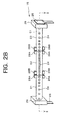
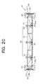
- FIGS. 2A , 2B , and 2C show the illuminating device 15 including a light guide unit 20, a light-emitting diode unit 25, and a holder 29.
- FIG. 2A shows the light guide unit 20 including a first light guide 21, a second light guide 22, and a third light guide 23.
- the first light guide 21, the second light guide 22, and the third light guide 23 are made of transparent resins such as acrylic and polycarbonate.
- the first light guide 21, the second light guide 22, and the third light guide 23 are all in the form of a cylinder having the same diameters.
- the first light guide 21, the second light guide 22, and the third light guide 23 each has the central axis line C1 that coincides with one another, and the first light guide 21, the second light guide 22, and the third light guide 23 are arranged in series, as each of side surfaces thereof being flush with each other.
- the side surface of the first light guide 21, that of the second light guide 22, and that of the third light guide 23 included in the light guide unit 20 have pieces of a light scattering layer 24 formed within the light guide across the direction of the central axis line C1 of the light guide in the form of a row.
- the light scattering layer 24 is a coated film, for example, formed by a white ink and the like and is formed by coating the surface of the light guide.
- the light emitted by the light-emitting diode unit 25 enters into the light guide unit 20 from the end portion thereof.
- the entering light decays the further the light is located from the end portion of the light guide unit 20.
- the pieces of the light scattering layer 24 are arranged for emission of the uniform outgoing light by the light emitter on the light guide unit 20.
- the pieces of the light scattering layer 24 may be arranged with spacing there between in the vicinity of the end portion on the light guide unit 20, while at around the center thereof, the pieces of the light scattering layer 24 may be arranged with narrower spacing. Further, the area of each piece of the light scattering layer 24 may be gradually increased from the end portion towards the center.
- FIG. 2A shows the first light guide 21 including a pair of mating members 28A, 28A provided on the side surface in the vicinity of an end surface 211, that is abutted (close proximity) against the second light guide 22.
- the pair of mating members 28A, 28A is serving as means for alignment (a first alignment member).
- the pair of mating members 28A, 28A is fixed to the side surface of the first light guide 21 using adhesion and the like.
- the first mating members 28A, 28A are arranged in line symmetry about the central axis line C1.
- the first mating member 28A is a substantially cuboid member having one surface thereof concaved to fit into the shape of side surfaces on the first light guide 21.
- the first mating member 28A has a circular through hole 28a.
- the through hole 28a is formed to have a central axis line C2 extend in the same direction as the central axis line C1.
- the second light guide 22 includes a pair of second mating members 28B, 28B provided on side surfaces in the vicinity of an end surface 222 that is abutted (close proximity) against the first light guide 21.
- the pair of second mating members 28B, 28B serves as means for alignment (a second alignment member).
- the pair of second mating members 28B, 28B is fixed to the side surface of the second light guide 22 using the adhesion and the like.
- the second mating members 28B, 28B are arranged in line symmetry about the central axis line C1.
- the second mating member 28B is a substantially cuboid member having one surface thereof concaved to fit into the shape of the side surface on the second light guide 22.
- the second mating member 28B has a cylindrical male portion 28b having a diameter substantially the same as that of the through hole 28a in the first light guide 21. Further, the male portion 28b is arranged to have its central axis C3 extend in the same direction with the central axis line C1 of the second light guide 22.
- the distance between the central axis line C3 of the male portion 28b and the central axis line C1 of the second light guide 22 coincides with the distance between the central axis line C2 of the through hole 28a in the first mating member 28A of the first light guide 21 and the central axis line C1 of the first light guide 21.
- FIG. 2A also shows the second light guide 22 further including a pair of first mating members 28A, 28A on the side surface in the vicinity of a surface 221 abutted (close proximity) against the third light guide 23.
- the pair of first mating members 28A, 28A is fixed to the side surfaces on the second light guide 22 using the adhesion or the like.
- the first mating members 28A, 28A are arranged in line symmetry bout the central axis line C1.
- the third light guide 23 also includes the pair of second mating members 28B, 28B on the side surface in the vicinity of an end surface 232 abutted (close proximity) against the second light guide 22.
- the pair of second mating members 28B, 28B is fixed to the side surface of the third light guide 23 using the adhesion or the like.
- the second mating members 28B, 28B are arranged in line symmetry about the central axis line C1.
- the pair of first mating members 28A, 28A provided on the second light guide 22 and the pair of second mating members 28B, 28B are respectively fixed to a location where, for example, a point at which the light scattering layer 24 on the side surface of the second light guide 22 is displaced by 90° about the origin, that is, the central axis line C1.
- the same arrangement applies to the pair of first mating members 28A, 28A provided on the first light guide 21, and the pair of second mating members 28B, 28B provided on the third light guide 23. With such structures, a light emission by each of the light guides is unhindered.
- FIG. 2A shows the light-emitting diode unit 25 representing a light source that is implemented with a light-emitting diode 27 on the board 26.
- FIGS. 2A and 2C show the holder 29 having a through hole 29a.
- the holder 29 provides support to the end portion of the light guide unit 20 with one opening of the through hole 29a. With such structures, the light emitted by the light-emitting diode 27 assuredly makes incidence on the end portion of the light guide unit 20.
- the holder 29 also provides support to the light-emitting diode unit 25 by the other opening of the through hole 29a.
- the illuminating device 15 is constituted by the first light guide 21, the second light guide 22, the third light guide 23, the light-emitting diode unit 25, and the holder 29 each having the aforementioned structures, that are assembled as follows.
- the end surface 211 on the first light guide 21, or the end surface 222 on the second light guide 22 is coated with a transparent adhesion (not shown) such as a UV curable resin. Then, the through hole 28a of the first mating member 28A in the first light guide 21 is aligned with the male portion 28b of the second mating member 28B in the second light guide 22.
- a transparent adhesion such as a UV curable resin
- end surface 211 of the first light guide 21 and the end surface 222 of the second light guide 22 are drawn close against each other to insert the male portion 28b on the second mating member 28B into the through hole 28a in the first mating member 28A. Yet further, the end surface 211 of the first light guide 21 and the end surface 222 of the second light guide 22 are drawn close against each other to have both end surfaces abutted (close proximity) all along the outer peripheries thereof as presented in FIG. 5 .
- the end surface 211 of the first light guide 21 and the end surface 222 of the second light guide 22 are connected together using the adhesion. This also allows the side surface of the first light guide 21 and the side surface of the second light guide 22 to be flush with each other.
- the second light guide 22 and the third light guide 23 are connected together by the same process used to connect the first light guide 21 with the second light guide 22 as described above.
- a final process involves an insertion of the end portion on the first light guide 21 or the end portion on the third light guide 23 into the one opening on the holder 29, and an installment of the light-emitting diode unit 25 on the other opening of the holder 29.
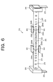
- the illuminating device 15 assembled according to the embodiment includes spacers 60 that are provided for covering the first mating member 28A and the second mating member 28B as presented in FIGS. 1 and 6 .
- the spacers 60 provide means for engaging the illuminating device 15 with the frame 11.
- the illuminating device 15 is installed on the frame 11 by having the spacers 60 engaged with an illuminating device installation section 11A formed on the frame 11 as presented in FIG. 1 .
- the image sensor 10 is assembled according to the descriptions above. Note that as seen in FIG. 1 , when the illuminating device 15 is provided to the frame 11, the illuminating device 15 is arranged in such a way that the light guide unit 20 has the central axis line C1 thereof coincide with the primary scan direction along the X axis direction of FIG. 1 . In the same way, the pieces of the light scatting layer 24 formed on the side surface of the light guide unit 20 are also arranged in a row with the primary scan direction along the X axis direction.
- the light-emitting diode 27 emits a light as soon as the electric power, not shown, for the contact image sensor 10 is turned ON.
- the emission of light enters into the light guide unit 20 and propagates within the light guide unit 20 in a longitudinal direction, that is, the central axis direction C1 of the light guide unit 20, as repeating a total reflection.
- a portion of the propagating light within the light guide unit 20 reaches the light scattering layer 24 formed on the side surface of the light guide unit 20.
- the light reaching the light scattering layer 24 exhibits a diffuse reflection, and a portion of the light is emitted toward the outside by the light emitter that is located at a location where the light scattering layer 24 on the side surface of the light guide unit 20 is displaced by 180° about the origin, that is, the central axis line C1 (see FIG. 1 , a dashed arrow; and FIG. 2C ).
- the pieces of the light scattering layer 24 formed on the side surface of the light guide unit 20 are provided in series with the X axis direction.
- the light emitter is formed on the side surface of the light guide unit 20 along the X axis direction and also in the shape of a straight line, with the light emitted from the scattering layer 24.
- the light guide unit 20 then emits a light in the shape of straight line via the light emitter in a direction perpendicular to the X axis.
- the light emitted from the light emitter on the light guide unit 20 passes through the transparent body 12 and provides the straight lined and the uniform illumination on the document M in the primary scan direction along the X axis direction as presented by the dashed arrow in FIG. 1 .
- the light irradiated by the light guide unit 20 and reflected off the document M is converged on the rod lens array 30.
- the light converged on the rod lens array 30 is photoelectrically converted by the sensor IC 40 on the sensor board 50.
- the sensor board 50 outputs an image signal to external components.
- the first light guide 21, the second light guide 22, and the third light guide 23 included in the light guide unit 20 respectively include either one of or both the first mating member 28A and the second mating member 28B to serve means for alignment (the first alignment member, the second alignment member, and the third alignment member).
- the end surfaces can be easily abutted (close proximity) against each other to have matching outer profiles of the end surfaces in each light guide, which also allows the side surfaces having the light emitters on the each light guide to be flush with each other.
- the light guide unit 20 is able to provide the straight lined and uniform illumination along the primary scan direction on the document positioning surface.
- the end surface on the third light guide 23 is abutted against the end surface of the second light guide 22, and the connection is made in the order of the first light guide 21, the second light guide 22, and the third light guide 23.
- connection may be made in the order of the third light guide 23, the first light guide 21, and the second light guide 22, after the end surface on the third light guide 23 is abutted against the end surface of the second light guide 22. Further, the side surface of the third light guide 23 and the side surface of the first light guide 21 are also flush with each other.
- Embodiment 2 employs the shape of the mating member on the light guide unit 20 that is different from that of Embodiment 1.
- FIGS. 7A and 7B show the first light guide 21 including a first mating member 28A and a third mating member 73 on the side surface in the vicinity of the end surface 211 abutted (close proximity) against the second light guide 22.
- the first mating member 28A and the third mating member 73 are provided to serve means for alignment.
- the first mating member 28A and the third mating member 73 are fixed to the side surface of the first light guide 21 using the adhesion and the like.
- the first mating member 28A and the third mating member 73 are arranged in line symmetry about the central axis line C1.
- FIGS. 7A and 7B present the first mating member 28A that is equivalent to that described in Embodiment 1.
- the third mating member 73 is a substantially cuboid member having one surface thereof being concaved to fit into the shape of the side surface on the first light guide 21.
- the third mating member 73 also includes a groove 73c. Further, the groove 73c is formed in the radius direction of the first light guide 21 and also in the same direction with the central axis direction C1 of the first light guide 21 as shown in FIG. 7B .
- FIGS. 8A and 8B show the second light guide 22 including the pair of second mating members 28B, 28B on the side surface in the vicinity of the end surface 222 that is abutted (close proximity) against the first light guide 21.
- the pair of second mating members 28B, 28B is provided to serve means for alignment.
- the pair of the second mating members 28B, 28B is fixed to the side surface on the second light guide 22 using the adhesion and the like. Further, the pair of second mating members 28B, 28B is arranged in line symmetry about the central axis line C1.
- the second mating member 28B referred in this embodiment has the same feature described in Embodiment 1.
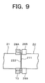
- the first light guide 21 and the second light guide 22 having the aforementioned structures are connected together in the same manner described in Embodiment 1. As shown in FIG. 9 , the groove 73c on the third mating member 73 and the male portion 28b on the second mating member 28B are fitted with each other while allowing for a backlash play in the radius direction of the first light guide 21 and the second light guide 22.
- the light guide unit 20 employs a hole in one of the mating members that is fitted in by the other mating member, and also employs a groove in the other mating member, whereby allowing the mating members to be fitted with each other regardless of dimension errors which may have occurred in the light guide and in the mating members.
- Embodiment 3 differs from the aforementioned Embodiment 1 in that Embodiment 3 employs the mating members on the end portion of the light guide unit.
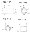
- the end surface 211 of the first light guide 21 that is abutted (close proximity) against the second light guide 22, has a concave portion 81 formed thereon.
- the concave portion 81 is provided to serve the means for alignment.
- the concave portion 81 employs a regular hexagon as viewed from the side surface relative to the central axis line C1.
- FIGS. 11A and 11B show the end surface 222 on the second light guide 22 that is abutted (close proximity) against the first light guide 21, has a convex portion 82 formed thereon.
- the convex portion 82 is provided to serve the means for alignment.
- the convex portion 82 employs a regular hexagon as viewed from the side surface relative to the central axis line C1.
- the convex portion 82 also employs the size approximately the same as that of the concave portion 81 on the first light guide 21 to have the convex portion 82 fitted with the concave portion 81.
- the first light guide 21 and the second light guide 22 having the aforementioned structures are connected as follows. Firstly, the end surface 211 on the first light guide 21 or the end surface 222 on the second light guide 22 is coated with the transparent adhesion (not shown) such as the UV curable resin. Then, the alignment between the concave portion 81 on the first light guide 21 and the convex portion 82 on the second light guide 22 is made. Further, the end surface 211 of the first light guide 21 and the end surface 222 of the second light guide 22 are drawn close against each other to have the convex portion 82 inserted into the concave portion 81a.
- the transparent adhesion not shown
- the end surface 211 of the first light guide 21 and the end surface 222 of the second light guide 22 are drawn close against each other to have the both end surfaces abutted (close proximity) all along the outer peripheries of the both end surfaces, as presented in FIG. 12 .
- the end surface 211 of the first light guide 21 and the end surface 222 of the second light guide 22 are connected together using the adhesion.
- FIG. 10A shows the side surface of the first light guide 21 includes convex members 85 formed thereon.
- the illuminating device 15 includes spacers arranged for covering the convex members 85.
- the spacers 86 are provided to serve as means for engagement to the frame 11.
- the illuminating device 15 is installed on the frame 11 by engaging the spacers 86 with the illuminating device installation section 11A formed on the frame 11 as shown in FIG. 13 .
- the light guide unit according to Embodiment 3 requires no engaging members on the side surface of the light guide as is required in the light guide unit according to Embodiment 1, thereby enabling the parts count reduction compared to the light guide unit according to Embodiment 1.
- Embodiment 4 differs from the aforementioned Embodiment 1 in that Embodiment 4 employs two light guides that constitute the light guide unit.
- FIG. 14 shows the illuminating device 100 including a light guide unit 101, the light-emitting diode unit 25, and the holder 29.
- the light guide unit 101 includes two light guides formed in the same way the light guide according to Embodiment 1 is formed.
- the light guide unit 101 includes a first light guide 110 and a second light guide 120.
- the first light guide 110 and the second light guide 120 each has the central axis line C1 that coincide with each other, and form the series arrangement such that the side surfaces are flush with each other.
- the first light guide 110 and the second light guide 120 are adjacent to each other, and also, each end surface on the first light guide 110 and the second light guide 120 is abutted (close proximity) against each other.
- the first light guide 110 also includes the pair of first mating members 28A, 28A on the side surface in the vicinity of the end surface that is abutted (close proximity) against the second light guide 120, in the same way with the first light guide 21 in Embodiment 1.
- the second light guide 120 which also includes the pair of second mating members 28B, 28B on the side surface in the vicinity of the end surface on the first light guide 110, in the same way with the second light guide 22 in Embodiment 1.
- the first light guide 110 and the second light guide 120 are connected together according to the same process described in Embodiment 1.
- the light guide unit according to Embodiment 4 may implement two light guides as the number of the light guide included is not limited to three.
- Embodiment 5 differs from the aforementioned Embodiment 1 in that Embodiment 5 employs n (where n is an integer equal to or greater than 3) light guides constituting the light guide unit.
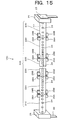
- FIG. 15 shows the illuminating device 150 including a light guide unit 200, the light-emitting diode unit 25, and the holder 29.
- the light guide unit 200 includes n (where n is an integer equal to or greater than 3) light guides that are formed by the same process used in forming the light guide according to Embodiment 1.
- the light guide unit 200 further includes the first light guide 210, the third light guide 230, and (n-2) second light guides 220 provided between the first light guide 210 and the third light guide 230 that are arranged in series.
- the first light guide 210, the third light guide 230, and the second light guides 220 each has the central axis line C1 that coincides with one another, and each surface thereof is lined up to form a flush-surface.
- the first light guide 210, the third light guide 230, and the second light guide 220 are abutted (close proximity) with each other on the adjacent end surfaces of the light guides.
- the first light guide 210 includes the pair of first mating members 28A, 28A on the side surface in the vicinity of the end surface that is abutted (close proximity) against the second light guide 220 as in the same manner for the first light guide 21 in Embodiment 1.
- the second light guide 220 includes the pair of mating members 28B, 28B on the side surface in the vicinity of the end surface of the first light guide 210, as in the same manner for the second light guide 22 in Embodiment 1.
- the second light guide 220 also includes the pair of first mating members 28A, 28A on the side surface in the vicinity of the end surface on the third light guide 230.
- the third light guide 230 includes the pair of second mating members 28B, 28B on the side surface in the vicinity of the end surface that is abutted (close proximity) against the second light guide 220, in the same manner for the third light guide 23 in Embodiment 1.
- the first light guide 210, the second light guide 220, and the third light guide 230 are connected together according to the same process described in Embodiment 1.
- the light guide unit according to Embodiment 5 may employ equal to or greater than three light guides as the number of light guides included is not limited to three as though such limitation is applied to Embodiment 1.
- the aforementioned embodiments have employed the cylinder-shaped light guide; however, the shapes of the end surface and the cross sections in the light guide are not particularly limited as such and thus, polygonal columns, e.g., a quadrangular prism may certainly be employed. Alternatively, a planar shape may also be employed by cutting across the side surface of the cylindrical light guide in a direction parallel to the central axis line C1 as shown in FIG. 15 .
- the aforementioned second light guides 22 and 220 have been described to include two types of mating members, that is, the first mating member 28A that is provided in the vicinity of one of the end portions, and the second mating member 28B that is provided in the vicinity of the other end portion thereof, yet the present disclosure is not limited to such particular structure.
- first mating member 28A is provided on one of the adjacent light guides and the second mating member 28B is provided on the other light guide, and these mating members are allowed to be fitted together, then the second light guides 22 and 220 may be employed with the same mating members in the vicinity of both ends.
- the present disclosure is suitable in optical instruments such as image scanners and the like.
Landscapes
- Engineering & Computer Science (AREA)
- Multimedia (AREA)
- Signal Processing (AREA)
- Physics & Mathematics (AREA)
- Optics & Photonics (AREA)
- General Physics & Mathematics (AREA)
- Power Engineering (AREA)
- Condensed Matter Physics & Semiconductors (AREA)
- Electromagnetism (AREA)
- Computer Hardware Design (AREA)
- Microelectronics & Electronic Packaging (AREA)
- Facsimile Heads (AREA)
- Facsimile Scanning Arrangements (AREA)
- Arrangement Of Elements, Cooling, Sealing, Or The Like Of Lighting Devices (AREA)
- Planar Illumination Modules (AREA)
Applications Claiming Priority (2)
| Application Number | Priority Date | Filing Date | Title |
|---|---|---|---|
| JP2012035955A JP5955021B2 (ja) | 2012-02-22 | 2012-02-22 | 導光体ユニット及びイメージセンサ |
| PCT/JP2013/053924 WO2013125501A1 (ja) | 2012-02-22 | 2013-02-19 | 導光体ユニット及びイメージセンサ |
Publications (1)
| Publication Number | Publication Date |
|---|---|
| EP2819389A1 true EP2819389A1 (en) | 2014-12-31 |
Family
ID=49005686
Family Applications (1)
| Application Number | Title | Priority Date | Filing Date |
|---|---|---|---|
| EP13751379.2A Withdrawn EP2819389A1 (en) | 2012-02-22 | 2013-02-19 | Light-guide unit and image sensor |
Country Status (6)
| Country | Link |
|---|---|
| US (1) | US20140374864A1 (ja) |
| EP (1) | EP2819389A1 (ja) |
| JP (1) | JP5955021B2 (ja) |
| KR (1) | KR20140111327A (ja) |
| CN (1) | CN104115477A (ja) |
| WO (1) | WO2013125501A1 (ja) |
Families Citing this family (3)
| Publication number | Priority date | Publication date | Assignee | Title |
|---|---|---|---|---|
| CN103149627B (zh) * | 2013-04-02 | 2016-05-25 | 深圳安嵘光电产品有限公司 | 一种带孔的导光板及其制作方法 |
| US10527780B2 (en) * | 2017-09-07 | 2020-01-07 | Canon Components, Inc. | Illumination apparatus, reading apparatus, and printing apparatus |
| DE102017219094A1 (de) * | 2017-10-25 | 2019-04-25 | Volkswagen Aktiengesellschaft | Leuchtvorrichtung für ein Kraftfahrzeug |
Family Cites Families (12)
| Publication number | Priority date | Publication date | Assignee | Title |
|---|---|---|---|---|
| US5969343A (en) * | 1995-08-24 | 1999-10-19 | Matsushita Electric Industrial Co., Ltd. | Linear illumination device |
| JP2001136343A (ja) * | 1999-11-09 | 2001-05-18 | Citizen Electronics Co Ltd | 密着形イメージセンサ |
| US6476986B2 (en) * | 1999-12-28 | 2002-11-05 | Texas Instruments Incorporated | Six-axis attachment apparatus and method for spatial light modulators |
| US7216990B2 (en) * | 2003-12-18 | 2007-05-15 | Texas Instruments Incorporated | Integrated lamp and aperture alignment method and system |
| US7344290B2 (en) * | 2005-09-20 | 2008-03-18 | Ledtech Electronics Corp. | Lamp module |
| CN101374188B (zh) * | 2007-08-22 | 2011-04-20 | 威海华菱光电有限公司 | 图像传感器 |
| JP2009117186A (ja) * | 2007-11-07 | 2009-05-28 | Rohm Co Ltd | 導光体、およびこれを用いたイメージセンサモジュール |
| JP2009303080A (ja) * | 2008-06-16 | 2009-12-24 | Nippon Sheet Glass Co Ltd | 棒状導光体および画像読取装置 |
| JP2010147859A (ja) * | 2008-12-19 | 2010-07-01 | Panasonic Corp | 線状照明装置及びそれを用いた密着型イメージセンサ及び画像読取システム |
| JP5251619B2 (ja) * | 2009-03-09 | 2013-07-31 | 三菱電機株式会社 | イメージセンサ |
| JP2010238492A (ja) * | 2009-03-31 | 2010-10-21 | Panasonic Corp | 照明装置 |
| JP2012015987A (ja) * | 2010-06-02 | 2012-01-19 | Rohm Co Ltd | 線状光源装置および画像読取装置 |
-
2012
- 2012-02-22 JP JP2012035955A patent/JP5955021B2/ja active Active
-
2013
- 2013-02-19 US US14/370,135 patent/US20140374864A1/en not_active Abandoned
- 2013-02-19 WO PCT/JP2013/053924 patent/WO2013125501A1/ja active Application Filing
- 2013-02-19 KR KR1020147021761A patent/KR20140111327A/ko not_active IP Right Cessation
- 2013-02-19 CN CN201380010001.8A patent/CN104115477A/zh active Pending
- 2013-02-19 EP EP13751379.2A patent/EP2819389A1/en not_active Withdrawn
Non-Patent Citations (1)
| Title |
|---|
| See references of WO2013125501A1 * |
Also Published As
| Publication number | Publication date |
|---|---|
| JP2013172366A (ja) | 2013-09-02 |
| CN104115477A (zh) | 2014-10-22 |
| KR20140111327A (ko) | 2014-09-18 |
| WO2013125501A1 (ja) | 2013-08-29 |
| JP5955021B2 (ja) | 2016-07-20 |
| US20140374864A1 (en) | 2014-12-25 |
Similar Documents
| Publication | Publication Date | Title |
|---|---|---|
| US9083832B2 (en) | Image reading device and method of manufacturing housing | |
| US8446647B2 (en) | Image reading device | |
| US7565050B2 (en) | Light pipe having an improved structure of prisms | |
| EP2115510B1 (en) | Light guide orientation connector | |
| JP2007322993A5 (ja) | ||
| EP2819389A1 (en) | Light-guide unit and image sensor | |
| WO2008108068A1 (ja) | 光走査装置及びそれを用いた二次元画像表示装置 | |
| TWI638195B (zh) | 光模組 | |
| US20110157516A1 (en) | Illuminating device and liquid crystal display device provided with the same | |
| US9088684B2 (en) | Image reading device | |
| US20130100657A1 (en) | Planar illuminating device | |
| US9557474B2 (en) | Light guide and image reading apparatus | |
| CN109196273B (zh) | 具有光导的照明布置 | |
| ATE539366T1 (de) | Faseroptischer scanner | |
| JP2013156337A (ja) | 光結合部材および光コネクタ | |
| CN110762479B (zh) | 车辆用灯具 | |
| JP5489689B2 (ja) | 照明装置及び内視鏡 | |
| JP6420030B2 (ja) | ライン状光照射装置 | |
| JP2014194918A (ja) | ライン状光照射装置 | |
| CN110778934B (zh) | 一种基于一维衍射的超薄平行光源 | |
| JP5400694B2 (ja) | 照明装置と導光材の固定構造 | |
| JP2018124418A (ja) | 光コネクタ | |
| JP5134471B2 (ja) | 発光装置 | |
| US20200382666A1 (en) | Image reading device | |
| JP2018160781A (ja) | 発光装置、画像読取装置及び画像形成装置 |
Legal Events
| Date | Code | Title | Description |
|---|---|---|---|
| PUAI | Public reference made under article 153(3) epc to a published international application that has entered the european phase |
Free format text: ORIGINAL CODE: 0009012 |
|
| 17P | Request for examination filed |
Effective date: 20140814 |
|
| AK | Designated contracting states |
Kind code of ref document: A1 Designated state(s): AL AT BE BG CH CY CZ DE DK EE ES FI FR GB GR HR HU IE IS IT LI LT LU LV MC MK MT NL NO PL PT RO RS SE SI SK SM TR |
|
| AX | Request for extension of the european patent |
Extension state: BA ME |
|
| DAX | Request for extension of the european patent (deleted) | ||
| STAA | Information on the status of an ep patent application or granted ep patent |
Free format text: STATUS: THE APPLICATION HAS BEEN WITHDRAWN |
|
| 18W | Application withdrawn |
Effective date: 20150723 |