EP2801435A2 - Pâte de soudure - Google Patents
Pâte de soudure Download PDFInfo
- Publication number
- EP2801435A2 EP2801435A2 EP20140167751 EP14167751A EP2801435A2 EP 2801435 A2 EP2801435 A2 EP 2801435A2 EP 20140167751 EP20140167751 EP 20140167751 EP 14167751 A EP14167751 A EP 14167751A EP 2801435 A2 EP2801435 A2 EP 2801435A2
- Authority
- EP
- European Patent Office
- Prior art keywords
- powder
- solder paste
- weight
- paste according
- layer
- Prior art date
- Legal status (The legal status is an assumption and is not a legal conclusion. Google has not performed a legal analysis and makes no representation as to the accuracy of the status listed.)
- Withdrawn
Links
Images


Classifications
-
- B—PERFORMING OPERATIONS; TRANSPORTING
- B23—MACHINE TOOLS; METAL-WORKING NOT OTHERWISE PROVIDED FOR
- B23K—SOLDERING OR UNSOLDERING; WELDING; CLADDING OR PLATING BY SOLDERING OR WELDING; CUTTING BY APPLYING HEAT LOCALLY, e.g. FLAME CUTTING; WORKING BY LASER BEAM
- B23K35/00—Rods, electrodes, materials, or media, for use in soldering, welding, or cutting
- B23K35/22—Rods, electrodes, materials, or media, for use in soldering, welding, or cutting characterised by the composition or nature of the material
- B23K35/24—Selection of soldering or welding materials proper
- B23K35/26—Selection of soldering or welding materials proper with the principal constituent melting at less than 400°C
-
- B—PERFORMING OPERATIONS; TRANSPORTING
- B22—CASTING; POWDER METALLURGY
- B22F—WORKING METALLIC POWDER; MANUFACTURE OF ARTICLES FROM METALLIC POWDER; MAKING METALLIC POWDER; APPARATUS OR DEVICES SPECIALLY ADAPTED FOR METALLIC POWDER
- B22F1/00—Metallic powder; Treatment of metallic powder, e.g. to facilitate working or to improve properties
- B22F1/09—Mixtures of metallic powders
-
- B—PERFORMING OPERATIONS; TRANSPORTING
- B22—CASTING; POWDER METALLURGY
- B22F—WORKING METALLIC POWDER; MANUFACTURE OF ARTICLES FROM METALLIC POWDER; MAKING METALLIC POWDER; APPARATUS OR DEVICES SPECIALLY ADAPTED FOR METALLIC POWDER
- B22F1/00—Metallic powder; Treatment of metallic powder, e.g. to facilitate working or to improve properties
- B22F1/17—Metallic particles coated with metal
-
- B—PERFORMING OPERATIONS; TRANSPORTING
- B23—MACHINE TOOLS; METAL-WORKING NOT OTHERWISE PROVIDED FOR
- B23K—SOLDERING OR UNSOLDERING; WELDING; CLADDING OR PLATING BY SOLDERING OR WELDING; CUTTING BY APPLYING HEAT LOCALLY, e.g. FLAME CUTTING; WORKING BY LASER BEAM
- B23K1/00—Soldering, e.g. brazing, or unsoldering
- B23K1/0008—Soldering, e.g. brazing, or unsoldering specially adapted for particular articles or work
- B23K1/0016—Soldering of electronic components
-
- B—PERFORMING OPERATIONS; TRANSPORTING
- B23—MACHINE TOOLS; METAL-WORKING NOT OTHERWISE PROVIDED FOR
- B23K—SOLDERING OR UNSOLDERING; WELDING; CLADDING OR PLATING BY SOLDERING OR WELDING; CUTTING BY APPLYING HEAT LOCALLY, e.g. FLAME CUTTING; WORKING BY LASER BEAM
- B23K35/00—Rods, electrodes, materials, or media, for use in soldering, welding, or cutting
- B23K35/02—Rods, electrodes, materials, or media, for use in soldering, welding, or cutting characterised by mechanical features, e.g. shape
- B23K35/0222—Rods, electrodes, materials, or media, for use in soldering, welding, or cutting characterised by mechanical features, e.g. shape for use in soldering or brazing
- B23K35/0244—Powders, particles or spheres; Preforms made therefrom
- B23K35/025—Pastes, creams or slurries
-
- B—PERFORMING OPERATIONS; TRANSPORTING
- B23—MACHINE TOOLS; METAL-WORKING NOT OTHERWISE PROVIDED FOR
- B23K—SOLDERING OR UNSOLDERING; WELDING; CLADDING OR PLATING BY SOLDERING OR WELDING; CUTTING BY APPLYING HEAT LOCALLY, e.g. FLAME CUTTING; WORKING BY LASER BEAM
- B23K35/00—Rods, electrodes, materials, or media, for use in soldering, welding, or cutting
- B23K35/22—Rods, electrodes, materials, or media, for use in soldering, welding, or cutting characterised by the composition or nature of the material
- B23K35/24—Selection of soldering or welding materials proper
- B23K35/26—Selection of soldering or welding materials proper with the principal constituent melting at less than 400°C
- B23K35/262—Sn as the principal constituent
-
- B—PERFORMING OPERATIONS; TRANSPORTING
- B23—MACHINE TOOLS; METAL-WORKING NOT OTHERWISE PROVIDED FOR
- B23K—SOLDERING OR UNSOLDERING; WELDING; CLADDING OR PLATING BY SOLDERING OR WELDING; CUTTING BY APPLYING HEAT LOCALLY, e.g. FLAME CUTTING; WORKING BY LASER BEAM
- B23K35/00—Rods, electrodes, materials, or media, for use in soldering, welding, or cutting
- B23K35/22—Rods, electrodes, materials, or media, for use in soldering, welding, or cutting characterised by the composition or nature of the material
- B23K35/24—Selection of soldering or welding materials proper
- B23K35/30—Selection of soldering or welding materials proper with the principal constituent melting at less than 1550°C
- B23K35/302—Cu as the principal constituent
-
- B—PERFORMING OPERATIONS; TRANSPORTING
- B23—MACHINE TOOLS; METAL-WORKING NOT OTHERWISE PROVIDED FOR
- B23K—SOLDERING OR UNSOLDERING; WELDING; CLADDING OR PLATING BY SOLDERING OR WELDING; CUTTING BY APPLYING HEAT LOCALLY, e.g. FLAME CUTTING; WORKING BY LASER BEAM
- B23K35/00—Rods, electrodes, materials, or media, for use in soldering, welding, or cutting
- B23K35/22—Rods, electrodes, materials, or media, for use in soldering, welding, or cutting characterised by the composition or nature of the material
- B23K35/36—Selection of non-metallic compositions, e.g. coatings or fluxes; Selection of soldering or welding materials, conjoint with selection of non-metallic compositions, both selections being of interest
- B23K35/3612—Selection of non-metallic compositions, e.g. coatings or fluxes; Selection of soldering or welding materials, conjoint with selection of non-metallic compositions, both selections being of interest with organic compounds as principal constituents
-
- C—CHEMISTRY; METALLURGY
- C22—METALLURGY; FERROUS OR NON-FERROUS ALLOYS; TREATMENT OF ALLOYS OR NON-FERROUS METALS
- C22C—ALLOYS
- C22C13/00—Alloys based on tin
-
- H—ELECTRICITY
- H05—ELECTRIC TECHNIQUES NOT OTHERWISE PROVIDED FOR
- H05K—PRINTED CIRCUITS; CASINGS OR CONSTRUCTIONAL DETAILS OF ELECTRIC APPARATUS; MANUFACTURE OF ASSEMBLAGES OF ELECTRICAL COMPONENTS
- H05K3/00—Apparatus or processes for manufacturing printed circuits
- H05K3/30—Assembling printed circuits with electric components, e.g. with resistors
- H05K3/32—Assembling printed circuits with electric components, e.g. with resistors electrically connecting electric components or wires to printed circuits
- H05K3/34—Assembling printed circuits with electric components, e.g. with resistors electrically connecting electric components or wires to printed circuits by soldering
- H05K3/346—Solder materials or compositions specially adapted therefor
-
- H—ELECTRICITY
- H10—SEMICONDUCTOR DEVICES; ELECTRIC SOLID-STATE DEVICES NOT OTHERWISE PROVIDED FOR
- H10W—GENERIC PACKAGES, INTERCONNECTIONS, CONNECTORS OR OTHER CONSTRUCTIONAL DETAILS OF DEVICES COVERED BY CLASS H10
- H10W72/00—Interconnections or connectors in packages
- H10W72/20—Bump connectors, e.g. solder bumps or copper pillars; Dummy bumps; Thermal bumps
-
- B—PERFORMING OPERATIONS; TRANSPORTING
- B22—CASTING; POWDER METALLURGY
- B22F—WORKING METALLIC POWDER; MANUFACTURE OF ARTICLES FROM METALLIC POWDER; MAKING METALLIC POWDER; APPARATUS OR DEVICES SPECIALLY ADAPTED FOR METALLIC POWDER
- B22F2998/00—Supplementary information concerning processes or compositions relating to powder metallurgy
- B22F2998/10—Processes characterised by the sequence of their steps
-
- H—ELECTRICITY
- H05—ELECTRIC TECHNIQUES NOT OTHERWISE PROVIDED FOR
- H05K—PRINTED CIRCUITS; CASINGS OR CONSTRUCTIONAL DETAILS OF ELECTRIC APPARATUS; MANUFACTURE OF ASSEMBLAGES OF ELECTRICAL COMPONENTS
- H05K2201/00—Indexing scheme relating to printed circuits covered by H05K1/00
- H05K2201/02—Fillers; Particles; Fibers; Reinforcement materials
- H05K2201/0203—Fillers and particles
- H05K2201/0263—Details about a collection of particles
- H05K2201/0272—Mixed conductive particles, i.e. using different conductive particles, e.g. differing in shape
-
- H—ELECTRICITY
- H05—ELECTRIC TECHNIQUES NOT OTHERWISE PROVIDED FOR
- H05K—PRINTED CIRCUITS; CASINGS OR CONSTRUCTIONAL DETAILS OF ELECTRIC APPARATUS; MANUFACTURE OF ASSEMBLAGES OF ELECTRICAL COMPONENTS
- H05K3/00—Apparatus or processes for manufacturing printed circuits
- H05K3/30—Assembling printed circuits with electric components, e.g. with resistors
- H05K3/32—Assembling printed circuits with electric components, e.g. with resistors electrically connecting electric components or wires to printed circuits
- H05K3/34—Assembling printed circuits with electric components, e.g. with resistors electrically connecting electric components or wires to printed circuits by soldering
- H05K3/3465—Application of solder
- H05K3/3485—Application of solder paste, slurry or powder
-
- H—ELECTRICITY
- H10—SEMICONDUCTOR DEVICES; ELECTRIC SOLID-STATE DEVICES NOT OTHERWISE PROVIDED FOR
- H10W—GENERIC PACKAGES, INTERCONNECTIONS, CONNECTORS OR OTHER CONSTRUCTIONAL DETAILS OF DEVICES COVERED BY CLASS H10
- H10W72/00—Interconnections or connectors in packages
- H10W72/01—Manufacture or treatment
- H10W72/013—Manufacture or treatment of die-attach connectors
- H10W72/01331—Manufacture or treatment of die-attach connectors using blanket deposition
- H10W72/01336—Manufacture or treatment of die-attach connectors using blanket deposition in solid form, e.g. by using a powder or by laminating a foil
-
- H—ELECTRICITY
- H10—SEMICONDUCTOR DEVICES; ELECTRIC SOLID-STATE DEVICES NOT OTHERWISE PROVIDED FOR
- H10W—GENERIC PACKAGES, INTERCONNECTIONS, CONNECTORS OR OTHER CONSTRUCTIONAL DETAILS OF DEVICES COVERED BY CLASS H10
- H10W72/00—Interconnections or connectors in packages
- H10W72/01—Manufacture or treatment
- H10W72/013—Manufacture or treatment of die-attach connectors
- H10W72/01351—Changing the shapes of die-attach connectors
- H10W72/01357—Changing the shapes of die-attach connectors by reflowing or heating
-
- H—ELECTRICITY
- H10—SEMICONDUCTOR DEVICES; ELECTRIC SOLID-STATE DEVICES NOT OTHERWISE PROVIDED FOR
- H10W—GENERIC PACKAGES, INTERCONNECTIONS, CONNECTORS OR OTHER CONSTRUCTIONAL DETAILS OF DEVICES COVERED BY CLASS H10
- H10W72/00—Interconnections or connectors in packages
- H10W72/071—Connecting or disconnecting
- H10W72/073—Connecting or disconnecting of die-attach connectors
- H10W72/07331—Connecting techniques
- H10W72/07336—Soldering or alloying
-
- H—ELECTRICITY
- H10—SEMICONDUCTOR DEVICES; ELECTRIC SOLID-STATE DEVICES NOT OTHERWISE PROVIDED FOR
- H10W—GENERIC PACKAGES, INTERCONNECTIONS, CONNECTORS OR OTHER CONSTRUCTIONAL DETAILS OF DEVICES COVERED BY CLASS H10
- H10W72/00—Interconnections or connectors in packages
- H10W72/071—Connecting or disconnecting
- H10W72/073—Connecting or disconnecting of die-attach connectors
- H10W72/07351—Connecting or disconnecting of die-attach connectors characterised by changes in properties of the die-attach connectors during connecting
- H10W72/07353—Connecting or disconnecting of die-attach connectors characterised by changes in properties of the die-attach connectors during connecting changes in shapes
-
- H—ELECTRICITY
- H10—SEMICONDUCTOR DEVICES; ELECTRIC SOLID-STATE DEVICES NOT OTHERWISE PROVIDED FOR
- H10W—GENERIC PACKAGES, INTERCONNECTIONS, CONNECTORS OR OTHER CONSTRUCTIONAL DETAILS OF DEVICES COVERED BY CLASS H10
- H10W72/00—Interconnections or connectors in packages
- H10W72/30—Die-attach connectors
- H10W72/321—Structures or relative sizes of die-attach connectors
- H10W72/325—Die-attach connectors having a filler embedded in a matrix
-
- H—ELECTRICITY
- H10—SEMICONDUCTOR DEVICES; ELECTRIC SOLID-STATE DEVICES NOT OTHERWISE PROVIDED FOR
- H10W—GENERIC PACKAGES, INTERCONNECTIONS, CONNECTORS OR OTHER CONSTRUCTIONAL DETAILS OF DEVICES COVERED BY CLASS H10
- H10W72/00—Interconnections or connectors in packages
- H10W72/30—Die-attach connectors
- H10W72/331—Shapes of die-attach connectors
- H10W72/334—Cross-sectional shape, i.e. in side view
-
- H—ELECTRICITY
- H10—SEMICONDUCTOR DEVICES; ELECTRIC SOLID-STATE DEVICES NOT OTHERWISE PROVIDED FOR
- H10W—GENERIC PACKAGES, INTERCONNECTIONS, CONNECTORS OR OTHER CONSTRUCTIONAL DETAILS OF DEVICES COVERED BY CLASS H10
- H10W72/00—Interconnections or connectors in packages
- H10W72/30—Die-attach connectors
- H10W72/351—Materials of die-attach connectors
- H10W72/352—Materials of die-attach connectors comprising metals or metalloids, e.g. solders
-
- H—ELECTRICITY
- H10—SEMICONDUCTOR DEVICES; ELECTRIC SOLID-STATE DEVICES NOT OTHERWISE PROVIDED FOR
- H10W—GENERIC PACKAGES, INTERCONNECTIONS, CONNECTORS OR OTHER CONSTRUCTIONAL DETAILS OF DEVICES COVERED BY CLASS H10
- H10W72/00—Interconnections or connectors in packages
- H10W72/30—Die-attach connectors
- H10W72/351—Materials of die-attach connectors
- H10W72/353—Materials of die-attach connectors not comprising solid metals or solid metalloids, e.g. ceramics
-
- H—ELECTRICITY
- H10—SEMICONDUCTOR DEVICES; ELECTRIC SOLID-STATE DEVICES NOT OTHERWISE PROVIDED FOR
- H10W—GENERIC PACKAGES, INTERCONNECTIONS, CONNECTORS OR OTHER CONSTRUCTIONAL DETAILS OF DEVICES COVERED BY CLASS H10
- H10W72/00—Interconnections or connectors in packages
- H10W72/90—Bond pads, in general
- H10W72/941—Dispositions of bond pads
- H10W72/944—Dispositions of multiple bond pads
-
- H—ELECTRICITY
- H10—SEMICONDUCTOR DEVICES; ELECTRIC SOLID-STATE DEVICES NOT OTHERWISE PROVIDED FOR
- H10W—GENERIC PACKAGES, INTERCONNECTIONS, CONNECTORS OR OTHER CONSTRUCTIONAL DETAILS OF DEVICES COVERED BY CLASS H10
- H10W90/00—Package configurations
- H10W90/701—Package configurations characterised by the relative positions of pads or connectors relative to package parts
- H10W90/731—Package configurations characterised by the relative positions of pads or connectors relative to package parts of die-attach connectors
- H10W90/736—Package configurations characterised by the relative positions of pads or connectors relative to package parts of die-attach connectors between a chip and a stacked lead frame, conducting package substrate or heat sink
Definitions
- Embodiments relate to a solder paste as an admixture of solder powder and a flux for soldering.
- Reflow soldering is used for internal bonding of electronic components in consideration of fine bonding parts.
- a solder paste used in reflow soldering is an admixture of solder powder and a flux for soldering.
- Pb-free solder refers to solder powder that does not include Pb and combines two or more elements of Sn, Ag, Sb, Cu, Zn, Bi, Ni, Cr, Fe, P, Ge, Ga, and the like with each other.
- soldering temperature is within a range of about 240°C-250°C when using Sn-Ag based alloys, Pb-free solder requires a high solidus temperature of at least 250°C.
- Embodiments provide a solder paste that may enhance wettability and restrict void generation.
- a solder paste comprises a flux, and a mixed powder mixed with the flux, the mixed powder includes first powder and second powder mixed with each other, the first powder includes tin and at least one metal dissolved in the tin, and the second powder includes copper powder, the surface of which is coated with silver.
- the at least one metal may include copper and silver.
- the first powder may include an alloy of tin, silver, and copper.
- the weight of the second powder may be in a range of 5% to 40% of the weight of the mixed powder.
- the weight of silver coating included in the second powder may be in a range of 10% to 50% of the weight of copper powder included in the second powder.
- the diameter of the copper powder included in the second powder may be in a range of 2 ⁇ m to 25 ⁇ m.
- the thickness of silver coating included in the second powder may be 1 ⁇ m or less.
- the at least one metal may include at least one of silver (Ag), copper (Cu), antimony (Sb), bismuth (Bi), indium (In), and zinc (Zn).
- a ratio of the weight percentage of tin to silver to copper included in the first powder may be 96.5:3:0.5.
- the first powder may be formed by breaking an alloy lump of tin, silver, and copper.
- An oxidation initiation temperature of the second powder may be 219°C or more.
- An oxidation initiation temperature of the second powder may be higher than a range of 240°C to 250°C.
- the flux may be liquid-phase, a solid having ductility, or a solid.
- the flux may include rosin, a thinner, and an activator.
- the activator may be present in an amount of 30% to 70% based on the total weight of the flux.
- the flux may further include a gelant, and the gelant may present in an amount of 0.1 % to 10% based on the total weight of the flux.
- the activator may further include a halogenated compound.
- the diameter of the copper powder may be in a range of 4 ⁇ m to 7 ⁇ m.
- a solder paste comprises a flux, and a mixed powder mixed with the flux, the mixed powder including first powder and second powder mixed with each other, wherein the first powder includes tin and at least one metal dissolved in the tin, and the second powder includes copper powder and a barrier coating film coated on the surface of the copper powder, and wherein the melting temperature of the barrier coating film is equal to or higher than that of the tin.
- the barrier coating film may be a silver coating film.
- An oxidation initiation temperature of the second powder may be higher than the eutectic point of the first powder.
- a solder paste comprises a flux, and a mixed powder mixed with the flux, the powder including first powder and second powder mixed with each other, wherein the first powder includes tin, silver, and copper, wherein the second powder includes copper powder and a silver coating film over the entire surface of the copper powder, wherein the weight of the second powder is in a range of 5% to 40% of the weight of the mixed powder, and wherein the weight of the silver coating film included in the second powder is in a range of 10% to 50% of the weight of the copper powder included in the second powder.
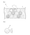
- FIG. 1 shows a conceptual view of a solder paste 100 according to an embodiment
- FIG. 2 shows an enlarged view of first powder 10 shown in FIG. 1
- FIG. 3 shows an enlarged view of second powder 20 shown in FIG. 1 .
- the solder paste 100 may include mixed powder 5 and a flux 30, and may take the form of an admixture of the mixed powder 5 and the flux 30.
- the mixed powder 5 may be solder powder, and may be a mixture of the first powder 10 and the second powder 20.
- the flux 30 serves to prevent oxidation at the surface of a base metal (for example, a substrate, see 105 in FIGs. 12A and 12B ) or a component that will come into contact with the base metal (see 210 in FIGs. 12A and 12B ) during reflow soldering, thereby enhancing adhesion between the base metal and the component during soldering.
- a base metal for example, a substrate, see 105 in FIGs. 12A and 12B
- a component that will come into contact with the base metal see 210 in FIGs. 12A and 12B
- the flux 30 may be liquid-phase, a solid having ductility, or a solid.
- the flux 30 may include rosin, a thinner, an activator, and the like.
- the thinner has volatility and thus is evaporated.
- the rosin and the activator remain as solid residues.
- the rosin may be used as a subacid activator, and may be added to prevent oxidation of a metal.
- the rosin may be one or more materials selected from among disproportionated rosin, hydrogenated rosin, dehydrogenated rosin, and non-modified rosin.
- the activator may serve to decompose or remove an oxide film that may be present on a portion of a substrate to be soldered (for example, oxidized copper or an oxide of solder on a PCB substrate).
- the flux 50 may further selectively include a halogenated compound that discharges hydrogenhalides when being heated.
- the halogenated compound may be selected from the group consisting of trans-2, 3-dibromo-2-buten-1, 4-diol, meso-2, 3-dibromosuccinate, tris-(2,3-dibromopropyl) isocyanurate, and combinations thereof.
- the flux 30 may be formed by distributing the activator, gelant, resin, and the like in a solvent.
- the used term "resin” may include a natural resin, such as rosin, chemically modified rosin, and a synthetic resin.
- the rosin may be a natural material acquired from a natural source, such as pine sap, and may contain an isomer of an abietic acid.
- the flux 30 may include the activator present in an amount of 30% ⁇ 70% based on the total weight of a composition, more particularly in an amount of 40% ⁇ 60%.
- the flux 30 may include the gelant present in an amount of 0.1% ⁇ 10% based on the total weight of a composition, more particularly in an amount of 0.4% ⁇ 1 %.
- the rheology of the flux 30 may depend on the level of the gelant present in the flux 30, and the flux 30 may have Newtonian rheology.
- the first powder 10 may include tin (Sn) as a main component and may be an alloy of Sn and a metal dissolved in Sn.
- the metal dissolved in Sn may include at least one of silver (Ag), copper (Cu), antimony (Sb), bismuth (Bi), indium (In), and zinc (Zn).
- the first powder 10 may be composed of tin (Sn), silver (Ag), and copper (Cu), and may be acquired by converting an alloy lump of Sn, Ag, and Cu into a powder form.
- the ratio of weight percentage of Sn to Ag to Cu in the first powder 10 may be 96.5:3:0.5, without being limited thereto.
- the second powder 20 may be powder in which Ag is coated on the surface of a metal dissolved in Sn.
- the second powder 20 may be Cu powder, the surface of which is coated with Ag.
- Ag may be coated on the entire surface the Cu powder 22 or the entire circumferential surface of the Cu powder 22.
- the second powder 20 may be acquired by forming a Ag coating film 24 on the surface of the Cu powder 22.
- the Ag coating film 24 may be formed using plating, precipitation in an aqueous solution, or the like.
- the Ag coating film 24 may serve as a barrier to prevent diffusion of Sn to the surface of the Cu powder 22.
- a reflow soldering process may be implemented as follows.
- solder paste 10 After the solder paste 10 is applied to a location to be soldered, the applied solder paste 100 is heated to a temperature of 240°C ⁇ 250°C.
- Sn included in the first powder 10 may be molten, and the molten Sn may form an intermetallic compound via reaction with Ag and Cu included in the first powder 10.
- the molten Sn may form Ag 3 Sn via reaction with Ag included in the first powder 10, and the molten Sn may form Cu 3 Sn, Cu 6 Sn 5 , or the like via reaction with Cu included in the first powder 10.
- the molten Sn may not immediately react with the Cu powder 22 of the second powder 20. That is, the molten Sn may not directly react with the Cu powder 22 due to the Ag coating film 24, and may form an intermetallic compound (for example, Ag 3 Sn) via reaction with the Ag coating film 24. Reaction of the molten Sn and the Cu 22 occurs only after the Ag coating film 24 is removed via the above-described reaction so that Cu 22 is exposed from the Ag coating film 24, thus forming an intermetallic compound.
- an intermetallic compound for example, Ag 3 Sn
- the Ag coating film 24 may serve to restrict or delay reaction between the molten Sn of the first powder 10 and the Cu 22 of the second powder 20.
- FIG. 4 shows activation energy upon reaction of Cu and Sn and activation energy upon reaction of Ag and Sn.
- first activation energy upon reaction of Cu and Sn is 28kJ/mol and second activation energy upon reaction of Ag and Sn is 52.6kJ/mol. That is, since the second activation energy is about two times the first activation energy, diffusion of Ag into Sn or reaction of Ag with Sn may progress slower than diffusion of Cu into Sn or reaction of Cu with Sn.
- the Ag coating film 24 formed on the surface of the Cu powder 22 restricts diffusion of Sn to the Cu powder 22 during reflow soldering, which may provide a location to be Sn soldered with sufficient wetting time, resulting in enhanced wettability.
- the embodiment may restrict void generation in a solder layer that is generated after soldering.
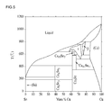
- FIG. 5 shows a first phase diagram for the Sn of the first powder 10 and the Cu 22 of the second powder 20
- FIG. 6 shows a second phase diagram for the Sn of the first powder and the Ag 24 of the second powder 20.
- a diameter D1 of the Cu powder 22 and a thickness D2 of the Ag coating film 24 may be adjusted to enhance wettability and to restrict void generation in a solder layer.
- the weight of the second powder 20 may be in a range of 5% ⁇ 40% of the total weight of the mixed powder 5. When the weight of the second powder 20 is below 5%, remelting prevention may not be achieved. When the weight of the second powder 20 exceeds 40%, the reaction amount of the second powder 20 with the first powder 10 is excessively increased, which may make it difficult to achieve sufficient wettability, thus generating numerous voids in the solder layer.
- the weight of the Ag coating film 24 may be in a range of 10% ⁇ 50% of the weight of the Cu powder 22.
- oxidation initiation temperature a temperature at which oxidation of the second powder 20 begins
- the eutectic point of the first powder 10 for example, about 213°C
- the diameter D1 of the Cu powder 22 may be in a range of 2 ⁇ m - 25 ⁇ m, more particularly in a range of 4 ⁇ m - 7 ⁇ m.
- the thickness D2 of the Ag coating film 24 may be 1 ⁇ m or less, without being limited thereto. Although the thickness D2 of the Ag coating film 24 may exceed 1 ⁇ m in another embodiment, an excessively thick thickness D2 of the Ag coating film 24 may increase the price of the solder paste 100. Since numerous voids are generated in the solder layer when the oxidation initiation temperature of the second powder 20 is lower than the eutectic point of the first powder 10, the weight of the second powder 20, the diameter D1 of the Cu powder 22, and the thickness D2 of the Ag coating film 24 must be determined such that the oxidation initiation temperature of the second powder 20 is higher than the eutectic point of the first powder 10.
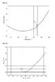
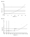
- FIG. 7A shows variation of heat flow depending on the temperature of the second powder 20 according to a first embodiment
- FIG. 7B shows variation of weight depending on the temperature of the second powder 20 shown in FIG. 7A .
- FIGs. 7A and 7B show a case in which the diameter D1 of the Cu powder 22 is 4 ⁇ m, the weight of the second powder 20 is 10% of the weight of the mixed powder 5, and the thickness D2 of the Ag coating film 24 is 0.1 ⁇ m.
- the oxidation initiation temperature of the second powder 20 may be estimated as about 221 °C in consideration of the heat flow of the second powder 20 being rapidly increased from about 221 °C.
- the oxidation initiation temperature of the second powder 20 may be estimated as about 219°C in consideration of the weight of the second powder 20 beginning to increase from about 219°C.
- the oxidation initiation temperature of the second powder 20 of the solder paste 100 according to the first embodiment is at least higher than the eutectic point of the first powder 10 (for example, about 213°C).
- Sn of the first powder 10 may be present in liquid phase during reflow soldering because the oxidation initiation temperature of the second powder 20 is at least higher than the eutectic point of the first powder 10.
- the liquid-phase Sn prevents reaction of the first powder 10 with oxygen during reflow soldering, and therefore the second powder 20 of the solder paste 100 according to the first embodiment is not substantially oxidized during reflow soldering.
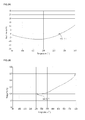
- FIG. 8A shows variation of heat flow depending on the temperature of the second powder 20 according to a second embodiment
- FIG. 8B shows variation of weight depending on the temperature of the second powder 20 shown in FIG. 8A .
- FIGs. 8A and 8B show a case in which the diameter D1 of the Cu powder 22 is 4 ⁇ m, the weight of the second powder 20 is 15% of the weight of the mixed powder 5, and the thickness D2 of the Ag coating film 24 is 0.2 ⁇ m.
- the oxidation initiation temperature of the second powder 20 may be estimated as about 259.62°C in consideration of the heat flow of the second powder 20 being rapidly increased from about 259.62°C.
- the oxidation initiation temperature of the second powder 20 may be estimated as about 258.70°C in consideration of the weight of the second powder 20 beginning to increase from about 258.70°C.
- the oxidation initiation temperature of the second powder 20 of the solder paste 100 according to the second embodiment is higher than reflow soldering temperature (for example, 240°C ⁇ 250°C) and thus oxidation of the second powder 20 does not occur at the reflow soldering temperature (for example, 240°C - 250°C).
- FIG. 9A shows variation of heat flow depending on the temperature of the second powder 20 according to a third embodiment
- FIG. 9B shows variation of weight depending on the temperature of the second powder 20 shown in FIG. 9A .
- FIGs. 9A and 9B show a case in which the diameter D1 of the Cu powder 22 is 7 ⁇ m, the weight of the second powder 20 is 12% of the weight of the mixed powder 5, and the thickness D2 of the Ag coating film 24 is 0.2 ⁇ m.
- the oxidation initiation temperature of the second powder 20 may be estimated as about 273.17°C in consideration of the heat flow of the second powder 20 being rapidly increased from about 273.17°C.
- the oxidation initiation temperature of the second powder 20 may be estimated as about 260.72°C in consideration of the weight of the second powder 20 beginning to increase from about 260.72°C.
- the oxidation initiation temperature of the second powder 20 of the solder paste 100 according to the third embodiment is higher than reflow soldering temperature (for example, 240°C ⁇ 250°C) and thus oxidation of the second powder 20 does not occur at the reflow soldering temperature (for example, 240°C ⁇ 250°C).
- FIG. 10A shows variation of heat flow depending on the temperature of the second powder 20 according to a fourth embodiment
- FIG. 10B shows variation of weight depending on the temperature of the second powder 20 shown in FIG. 10A .
- FIGs. 10A and 10B show a case in which the diameter D1 of the Cu powder 22 is 7 ⁇ m, the weight of the second powder 20 is 20% of the weight of the mixed powder 5, and the thickness D2 of the Ag coating film 24 is 0.4 ⁇ m.
- a rapid increase in the heat flow of the second powder 20 is not observed at a temperature of 350°C or less.
- the oxidation initiation temperature of the second powder 20 may be estimated as about 286.24°C in consideration of the weight of the second powder 20 beginning to increase from about 286.24°C.
- the oxidation initiation temperature of the second powder 20 of the solder paste 100 according to the fourth embodiment is higher than reflow soldering temperature (for example, 240°C ⁇ 250°C) and thus oxidation of the second powder 20 does not occur at the reflow soldering temperature (for example, 240°C ⁇ 250°C).
- FIG. 11A shows variation of heat flow depending on the temperature of the second powder 20 according to a fifth embodiment
- FIG. 11B shows variation of weight depending on the temperature of the second powder 20 shown in FIG. 11A .
- FIGs. 11A and 11B show a case in which the diameter D1 of the Cu powder 22 is 7 ⁇ m, the weight of the second powder 20 is 30% of the weight of the mixed powder 5, and the thickness D2 of the Ag coating film 24 is 0.6 ⁇ m.
- a rapid increase in the heat flow of the second powder 20 is not observed at a temperature of 350°C or less.
- the oxidation initiation temperature of the second powder 20 may be estimated as about 299.88°C in consideration of the weight of the second powder 20 beginning to increase from about 299.88°C.
- the oxidation initiation temperature of the second powder 20 of the solder paste 100 according to the fifth embodiment is at least higher than reflow soldering temperature (for example, 240°C ⁇ 250°C) and thus oxidation of the second powder 20 does not occur at the reflow soldering temperature (for example, 240°C ⁇ 250°C).
- a metal which may form a barrier coating film, serving to prevent diffusion of Sn of the first powder 10 to the surface of the Cu powder 22 of the second powder 20, must be dissolved in Sn, requires a melting temperature equal to or higher than that of Sn, and must not deteriorate solderability when dissolved in Sn.
- a coating film that satisfies the above-described conditions may be formed of Ag as in the embodiment, and nickel (Ni) may satisfy the above-described conditions.
- Ni is well oxidized at a temperature lower than the eutectic point of the first powder 10 (e.g., about 213°C), numerous voids may be generated in the solder layer after soldering.
- Ni may already be oxidized at a temperature equal to or less than the eutectic point of the first powder 10 (e.g., about 213°C)
- an Ni coating film of the second powder 20 may already be oxidized during reflow soldering, and thus numerous voids may be generated in the solder layer after soldering.
- numerous voids generated in the solder layer may increase electric resistance of the solder layer and deteriorate heat radiation, and reflow soldering may thus need to be performed under a nitrogen environment to prevent oxidation.
- the barrier coating film may be formed of Ag that is less sensitive to oxidation than Ni.
- the oxidation initiation temperature of the second powder 20 may become about 219°C or more, which is at least higher than the eutectic point of the first powder 10 (e.g., about 213°C), via adjustment of the weight of the second powder 20 and the thickness of the Ag coating film 24.
- the embodiment may restrict generation of voids in the solder layer and prevent increase in electric resistance and deterioration of heat radiation efficiency caused by voids because substantial oxidation of the second powder 20 does not occur at the reflow soldering temperature (about 240°C ⁇ 250°C).
- the embodiment may not be affected by a nitrogen environment and oxygen density during reflow soldering because substantial oxidation of the second powder 20 does not occur during reflow soldering.
- FIG. 12A shows a solder layer 110 using a general solder paste
- FIG. 12B shows a solder layer 120 using a solder paste according to the embodiment.
- solder layer 110 which bonds a base metal 105 and a component 210 as exemplarily shown in FIG. 12A , has numerous voids
- solder layer 120 between the base metal 105 and the component 210 as exemplarily shown in FIG. 12B has good wettability, thus ensuring smooth formation of a fillet 220 at a lateral side thereof and generating fewer voids.
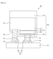
- FIG. 13 shows a sectional view of a light emitting device package 300 including a bonding part 360 using the solder paste according to the embodiment.
- the light emitting device package 300 may include a sub-mount 301, a light emitting device 302, and bonding parts 303.
- the sub-mount 301 supports the light emitting device 302, and the light emitting device 302 is mounted on the sub-mount 301.
- the sub-mount 301 may take the form of a package body or a printed circuit board, for example, and may have various other shapes to allow flip-chip bonding of the light emitting device 302.
- the sub-mount 301 may include a first conductive layer 382 and a second conductive layer 384, which are bonded to the light emitting device 302.
- the first conductive layer 382 and the second conductive layer 384 may be spaced apart from each other so as to be electrically isolated from each other.
- the light emitting device 302 is disposed on the sub-mount 301, and is electrically connected to the sub-mount 301 via the bonding parts 303.
- the light emitting device 302 includes a substrate 310, a light emitting structure 320, a conductive layer 330, a first electrode 342, a second electrode 344, and an insulation layer 350.
- the light emitting device 302 may be disposed on the sub-mount 301 such that the first electrode 342 and the second electrode 344 face the sub-mount 301.
- the light emitting structure 320 is located on one surface of the substrate 310.
- the substrate 310 may be a light transmitting substrate, such as, for example, any one of a sapphire substrate, a silicone (Si) substrate, a zinc oxide (ZnO) substrate, and a nitride semiconductor substrate, or may be a template substrate on which at least one of GaN, InGaN, AlGaN, AllnGaN, SiC, GaP, InP, Ga 2 O 3 , and GaAs is stacked.
- a light transmitting substrate such as, for example, any one of a sapphire substrate, a silicone (Si) substrate, a zinc oxide (ZnO) substrate, and a nitride semiconductor substrate, or may be a template substrate on which at least one of GaN, InGaN, AlGaN, AllnGaN, SiC, GaP, InP, Ga 2 O 3 , and GaAs is stacked.
- the light emitting structure 320 may include multiple group III-V compound semiconductor layers.
- the light emitting structure 320 may include a first conductive semiconductor layer 322, a second conductive semiconductor layer 326, and an active layer 324 between the first conductive semiconductor layer 322 and the second conductive semiconductor layer 326.
- a side surface of the light emitting structure 320 may be inclined by isolation etching for division on a per unit chip basis.
- the side surface of the light emitting structure 320 may have an inclination from a surface of the substrate 310.
- the first conductive semiconductor layer 322 may be formed of group III-V compound semiconductors and may be doped with a first conductive dopant.
- the first conductive semiconductor layer 322 may be formed of a semiconductor material having a composition equation of In x Al y Ga 1-x-y N (0 ⁇ x ⁇ 1, 0 ⁇ y ⁇ 1, 0 ⁇ x+y ⁇ 1), and for example, may be selected from among AlGaN, GaN, AIN, InGaN, InA, InAlGaN, AllnN, AlGaAs, GaP, GaAs, GaAsP, AlGalnP, and the like, and may be doped with an n-type dopant, such as Si, Ge, Sn, Te, or the like.
- the active layer 324 may generate light using energy generated during recombination of electrons and holes provided from the second conductive semiconductor layer 326 and the first conductive semiconductor layer 322.
- the active layer 324 may be formed of a semiconductor material having a composition equation of In x Al y Ga 1-x-y N (0 ⁇ x ⁇ 1, 0 ⁇ y ⁇ 1, 0 ⁇ x+y ⁇ 1).
- the active layer 324 may have any one of a single quantum well structure, a multi quantum well structure, a quantum-dot structure, or a quantum-wire structure.
- the active layer 324 may take the form of a stack of multiple well layers and multiple barrier layers.
- the well layer/barrier layer of the active layer 324 may have at least one pair configuration of InGaN/GaN, InGaN/InGaN, GaN/AlGaN, InAlGaN/GaN, GaAs(InGaAs)/AlGaAs, and GaP(InGaP)/AlGaP, without being limited thereto.
- the well layer may be formed of a material having a smaller energy band gap than that of the barrier layer.
- the second conductive semiconductor layer 326 may be formed of group III-V compound semiconductors and may be doped with a second conductive dopant.
- the second conductive semiconductor layer 326 may be formed of a semiconductor material having a composition equation of In x Al y Ga 1-x-y N (0 ⁇ x ⁇ 1, 0 ⁇ y ⁇ 1, 0 ⁇ x+y ⁇ 1), and for example, may be selected from among AlGaN, GaN, AIN, InGaN, InA, InAlGaN, AllnN, AlGaAs, GaP, GaAs, GaAsP, AlGalnP, and the like, and may be doped with a p-type dopant, such as Mg, Zn, Ca, Sr, Ba, or the like.
- a clad layer (not shown) doped with an n-type or p-type dopant may be formed between the active layer 324 and the first conductive semiconductor layer 322, or between the active layer 324 and the second conductive semiconductor layer 326.
- the clad layer may be a semiconductor layer including AlGaN or InAlGaN.
- the embodiment is not limited thereto.
- the first conductive semiconductor layer 322 may include a p-type semiconductor layer and the second conductive semiconductor layer 326 may include an n-type semiconductor layer.
- an n-type or p-type semiconductor layer may further be provided under the second conductive semiconductor layer 326.
- the light emitting structure 320 may include at least one of nn, pn, npn, and pnp bonding configurations.
- the dopants of the first conductive semiconductor layer 322 and the second conductive semiconductor layer 326 may have an even or uneven doping density. That is, the configuration of the light emitting structure 320 may be altered in various ways, and the light emitting structure 320 may emit light having various wavelengths.
- the conductive layer 330 may be disposed on the second conductive semiconductor layer 326.
- the conductive layer 330 may be located between the second conductive semiconductor layer 326 and the second electrode 344, and may be in ohmic contact with respect to the second conductive semiconductor layer 326.
- the conductive layer 330 may reduce total reflection and exhibit high light transmittance, thus increasing extraction efficiency of light from the active layer 324 to the second conductive semiconductor layer 326.
- the conductive layer 330 may be formed of at least one of a metal in ohmic contact with the second conductive semiconductor layer 326, for example, at least one of Au, Pd, Pt, Ru, Re, Mg, Zn, Hf, Ta, Rh, Ir, W, Ti, Ag, Cr, Mo, Nb, Al, Ni, Cu, WTi, V, or alloys thereof.
- the conductive layer 330 may be formed in a single layer or in multiple layers using a transparent oxide-based material exhibiting high transmittance at wavelengths of emitted light, for example, one or more of Indium Tin Oxide (ITO), Tin Oxide (TO), Indium Zinc Oxide (IZO), Indium Zinc Tin Oxide (IZTO), Indium Aluminum Zinc Oxide (IAZO), Indium Gallium Zinc Oxide (IGZO), Indium Gallium Tin Oxide (IGTO), Aluminum Zinc Oxide (AZO), Antimony Tin Oxide (ATO), Gallium Zinc Oxide (GZO), IrOx, RuOx, RuOx/ITO, Ni, Ag, Ni/IrOx/Au, or Ni/IrOx/Au/ITO.
- ITO Indium Tin Oxide
- TO Tin Oxide
- IZO Indium Zinc Oxide
- IZTO Indium Zinc Tin Oxide
- IAZO Indium Aluminum Zinc Oxide
- IGZO Indium Gallium Zin
- the light emitting structure 320 may have a region, through which a portion of the first conductive semiconductor layer 322 is exposed for arrangement of the first electrode 342.
- the light emitting structure 320 may include a region formed by partially etching the second conductive semiconductor layer 326, the active layer 324, and the first conductive semiconductor layer 322 so as to expose a portion of the first conductive semiconductor layer 322.
- the first electrode 342 may be disposed on the exposed portion of the first conductive semiconductor layer 322 to come into contact with the first conductive semiconductor layer 322.
- the second electrode 344 may be disposed on an upper surface of the conductive layer 330 to come into contact with the conductive layer 330.
- the first electrode 342 and the second electrode 344 may be formed of a conductive metal, for example, at least one of Au, Pd, Pt, Ru, Re, Mg, Zn, Hf, Ta, Rh, Ir, W, Ti, Ag, Cr, Mo, Nb, Al, Ni, Cu, WTi, V, or alloys thereof.
- the insulation layer 350 may be disposed on a side surface of the light emitting structure 320.
- the insulation layer 350 may cover the side surface of the light emitting structure 320.
- the insulation layer 350 may be disposed on the exposed remaining portion of the first conductive semiconductor layer 322 except for the portion where the first electrode 342 is disposed.
- the insulation layer 350 may be disposed on the exposed portion of the upper surface of the conductive layer 330 except for the portion where the second electrode 344 is disposed.
- the insulation layer 350 may exposed at least a portion of the upper surface of the first electrode 342 and at least a portion of the upper surface of the second electrode 344.
- the sub-mount 301 is located below the first electrode 342 and the second electrode 344.
- the sub mount 310 may include, for example, a printed circuit board formed of a resin, such as PolyPhthal Amide (PPA), Liquid Crystal Polymer (LCP), PolyAmide9T (PA9T), and the like, a metal, photosensitive glass, sapphire, ceramic, and the like.
- a resin such as PolyPhthal Amide (PPA), Liquid Crystal Polymer (LCP), PolyAmide9T (PA9T), and the like, a metal, photosensitive glass, sapphire, ceramic, and the like.
- PPA PolyPhthal Amide
- LCP Liquid Crystal Polymer
- PA9T PolyAmide9T
- the sub-mount 301 according to the embodiment is not limited to the above materials.
- the first conductive layer 382 and the second conductive layer 384 may be disposed on the upper surface of the sub-mount 301 so as to be spaced apart from each other.
- the upper surface of the sub-mount 301 may be a surface facing the light emitting device 302.
- the first conductive layer 382 and the first electrode 342 may be vertically aligned with each other, and the second conductive layer 384 and the second electrode 344 may be vertically aligned with each other.
- a vertical direction may be an alignment direction of the sub-mount 301 and the light emitting device 302.
- the bonding parts 303 may be located between the first conductive layer 382 and the first electrode 342 and between the second conductive layer 384 and the second electrode 344 to bond the same to each other.
- the bonding parts 303 may include a first bonding part 362 bonding the first conductive layer 382 and the first electrode 342 to each other, and a second bonding part 364 bonding the second conductive layer 384 and the second electrode 344 to each other.
- the first bonding part 362 and the second bonding part 364 may be solder using the solder paste 100 according to the embodiment.
- the first bonding part 362 and the second bonding part 364 may have the fillet 220 described in Fig.12B . That is, the light emitting device 302 may be flip-chip bonded to the sub-mount 301 using the solder paste 100 according to the embodiment.
- the embodiments may provide enhanced wettability and restricted void generation.
Landscapes
- Engineering & Computer Science (AREA)
- Mechanical Engineering (AREA)
- Manufacturing & Machinery (AREA)
- Microelectronics & Electronic Packaging (AREA)
- Chemical & Material Sciences (AREA)
- Materials Engineering (AREA)
- Metallurgy (AREA)
- Organic Chemistry (AREA)
- Electric Connection Of Electric Components To Printed Circuits (AREA)
Applications Claiming Priority (1)
| Application Number | Priority Date | Filing Date | Title |
|---|---|---|---|
| KR1020130053047A KR102156373B1 (ko) | 2013-05-10 | 2013-05-10 | 솔더 페이스트 |
Publications (2)
| Publication Number | Publication Date |
|---|---|
| EP2801435A2 true EP2801435A2 (fr) | 2014-11-12 |
| EP2801435A3 EP2801435A3 (fr) | 2015-03-04 |
Family
ID=50721590
Family Applications (1)
| Application Number | Title | Priority Date | Filing Date |
|---|---|---|---|
| EP20140167751 Withdrawn EP2801435A3 (fr) | 2013-05-10 | 2014-05-09 | Pâte de soudure |
Country Status (4)
| Country | Link |
|---|---|
| US (1) | US9610655B2 (fr) |
| EP (1) | EP2801435A3 (fr) |
| KR (1) | KR102156373B1 (fr) |
| CN (1) | CN104139249B (fr) |
Cited By (2)
| Publication number | Priority date | Publication date | Assignee | Title |
|---|---|---|---|---|
| CN109244686A (zh) * | 2018-07-26 | 2019-01-18 | 合德华厦安防科技有限公司 | 一种用于接地系统的芯棒及其制备方法 |
| EP3782764A1 (fr) * | 2019-08-19 | 2021-02-24 | Heraeus Deutschland GmbH & Co KG | Combinaison de pâte de cuivre / métal d'apport de brasage destinée à la production de composés de soudure sans plomb stables à température élevée |
Families Citing this family (9)
| Publication number | Priority date | Publication date | Assignee | Title |
|---|---|---|---|---|
| US9282638B2 (en) * | 2012-01-13 | 2016-03-08 | Zycube Co., Ltd. | Electrode, electrode material, and electrode formation method |
| KR102101474B1 (ko) | 2015-12-15 | 2020-04-16 | 주식회사 엘지화학 | 금속 페이스트 및 열전 모듈 |
| JP7145855B2 (ja) * | 2017-11-22 | 2022-10-03 | 深▲チェン▼市福英達工業技術有限公司 | マイクロ/ナノ粒子強化型複合はんだ及びその調製方法 |
| JP6509469B1 (ja) * | 2018-11-08 | 2019-05-08 | 三菱電機株式会社 | 接合構造体、半導体装置及びその製造方法 |
| US11581239B2 (en) * | 2019-01-18 | 2023-02-14 | Indium Corporation | Lead-free solder paste as thermal interface material |
| CN111571065B (zh) * | 2020-05-14 | 2021-04-13 | 深圳市唯特偶新材料股份有限公司 | 一种改善bga封装焊接性能的锡膏及其制备方法 |
| JP7656862B2 (ja) * | 2021-06-18 | 2025-04-04 | パナソニックIpマネジメント株式会社 | 導電性ペーストおよびそれを用いて形成される導電膜 |
| CN114055007B (zh) * | 2021-11-16 | 2023-03-14 | 陕西众森电能科技有限公司 | 一种超细低温焊锡粉、锡膏及其制备方法与应用 |
| CN114055008B (zh) * | 2021-11-18 | 2023-09-05 | 陕西众森电能科技有限公司 | 一种制备超细焊锡膏的金属粉、焊锡膏及其制备方法 |
Citations (3)
| Publication number | Priority date | Publication date | Assignee | Title |
|---|---|---|---|---|
| JPH05337688A (ja) * | 1992-06-10 | 1993-12-21 | Harima Chem Inc | ソルダペースト |
| JP3193962B2 (ja) * | 1992-06-25 | 2001-07-30 | 千住金属工業株式会社 | ソルダーペースト |
| US20030221748A1 (en) * | 2002-05-30 | 2003-12-04 | Fry's Metals, Inc. | Solder paste flux system |
Family Cites Families (10)
| Publication number | Priority date | Publication date | Assignee | Title |
|---|---|---|---|---|
| TW592871B (en) | 2000-12-21 | 2004-06-21 | Hitachi Ltd | Solder foil and semiconductor device and electronic device |
| JP4175857B2 (ja) | 2002-09-27 | 2008-11-05 | 株式会社Neomaxマテリアル | はんだ被覆ボールの製造方法 |
| JP4435663B2 (ja) * | 2004-10-04 | 2010-03-24 | 日本電波工業株式会社 | はんだ材料、電子部品、及び電子部品の製造方法 |
| JP4753090B2 (ja) | 2005-01-11 | 2011-08-17 | 株式会社村田製作所 | はんだペースト、及び電子装置 |
| KR101026970B1 (ko) | 2005-05-25 | 2011-04-11 | 센주긴조쿠고교 가부시키가이샤 | 납 프리 솔더 페이스트 |
| KR101233926B1 (ko) * | 2006-04-26 | 2013-02-15 | 센주긴조쿠고교 가부시키가이샤 | 솔더 페이스트 |
| KR101004589B1 (ko) | 2006-09-01 | 2010-12-29 | 센주긴조쿠고교 가부시키가이샤 | 기능 부품용 리드와 그 제조 방법 |
| CN102107340B (zh) * | 2009-12-24 | 2015-10-21 | 汉高股份有限及两合公司 | 一种焊膏组合物、焊膏及一种助焊剂 |
| JP2011147982A (ja) * | 2010-01-22 | 2011-08-04 | Nippon Dempa Kogyo Co Ltd | はんだ、電子部品、及び電子部品の製造方法 |
| JP2013081966A (ja) * | 2011-10-06 | 2013-05-09 | Fujitsu Ltd | 導電性接合材料、並びに導体の接合方法、及び半導体装置の製造方法 |
-
2013
- 2013-05-10 KR KR1020130053047A patent/KR102156373B1/ko not_active Expired - Fee Related
-
2014
- 2014-05-07 US US14/272,127 patent/US9610655B2/en active Active
- 2014-05-09 EP EP20140167751 patent/EP2801435A3/fr not_active Withdrawn
- 2014-05-09 CN CN201410194323.9A patent/CN104139249B/zh active Active
Patent Citations (3)
| Publication number | Priority date | Publication date | Assignee | Title |
|---|---|---|---|---|
| JPH05337688A (ja) * | 1992-06-10 | 1993-12-21 | Harima Chem Inc | ソルダペースト |
| JP3193962B2 (ja) * | 1992-06-25 | 2001-07-30 | 千住金属工業株式会社 | ソルダーペースト |
| US20030221748A1 (en) * | 2002-05-30 | 2003-12-04 | Fry's Metals, Inc. | Solder paste flux system |
Cited By (4)
| Publication number | Priority date | Publication date | Assignee | Title |
|---|---|---|---|---|
| CN109244686A (zh) * | 2018-07-26 | 2019-01-18 | 合德华厦安防科技有限公司 | 一种用于接地系统的芯棒及其制备方法 |
| CN109244686B (zh) * | 2018-07-26 | 2021-06-18 | 合德华厦安防科技有限公司 | 一种用于接地系统的芯棒及其制备方法 |
| EP3782764A1 (fr) * | 2019-08-19 | 2021-02-24 | Heraeus Deutschland GmbH & Co KG | Combinaison de pâte de cuivre / métal d'apport de brasage destinée à la production de composés de soudure sans plomb stables à température élevée |
| WO2021032350A1 (fr) * | 2019-08-19 | 2021-02-25 | Heraeus Deutschland GmbH & Co. KG | Procédé de fabrication d'une liaison par soudage |
Also Published As
| Publication number | Publication date |
|---|---|
| US9610655B2 (en) | 2017-04-04 |
| KR102156373B1 (ko) | 2020-09-16 |
| EP2801435A3 (fr) | 2015-03-04 |
| CN104139249A (zh) | 2014-11-12 |
| US20140332116A1 (en) | 2014-11-13 |
| CN104139249B (zh) | 2017-01-18 |
| KR20140133221A (ko) | 2014-11-19 |
Similar Documents
| Publication | Publication Date | Title |
|---|---|---|
| US9610655B2 (en) | Solder paste | |
| KR100974776B1 (ko) | 발광 소자 | |
| US20210167034A1 (en) | Chip arrangements | |
| JP5513707B2 (ja) | 半導体発光デバイスの相互接続 | |
| US9490147B2 (en) | Stud bump structure and method for manufacturing the same | |
| US20140273318A1 (en) | Method of forming metallic bonding layer and method of manufacturing semiconductor light emitting device therewith | |
| US20080136019A1 (en) | Solder Bump/Under Bump Metallurgy Structure for High Temperature Applications | |
| TWI496324B (zh) | 發光二極體封裝體 | |
| KR102601553B1 (ko) | 반도체 발광 소자 | |
| US12330243B2 (en) | Method of forming an intermetallic phase layer with a plurality of nickel particles | |
| KR101430673B1 (ko) | 반도체 디바이스 및 이의 다이 본딩 구조 | |
| JP5976379B2 (ja) | 電子機器及びその製造方法 | |
| US20070117475A1 (en) | Prevention of Sn whisker growth for high reliability electronic devices | |
| JP2005117035A (ja) | フリップチップ型窒化ガリウム系半導体発光素子およびその製造方法 | |
| JP6890707B1 (ja) | 半導体発光素子及び半導体発光素子の製造方法 | |
| US6653215B1 (en) | Contact to n-GaN with Au termination | |
| JP2012069545A (ja) | 発光素子の搭載方法 | |
| EP2383780A1 (fr) | Dispositifs électroluminescents | |
| JP2014003242A (ja) | ダイボンド材及び発光装置 | |
| US8853006B2 (en) | Method of manufacturing semiconductor device and semiconductor device | |
| KR101976450B1 (ko) | 발광 소자 및 발광 소자 패키지 | |
| US20250118696A1 (en) | Solder and semiconductor device | |
| US9308603B2 (en) | Solder, solder joint structure and method of forming solder joint structure | |
| TWI489596B (zh) | 晶片結構 | |
| JP2010161252A (ja) | 半導体装置およびその製造方法 |
Legal Events
| Date | Code | Title | Description |
|---|---|---|---|
| PUAI | Public reference made under article 153(3) epc to a published international application that has entered the european phase |
Free format text: ORIGINAL CODE: 0009012 |
|
| 17P | Request for examination filed |
Effective date: 20140603 |
|
| AK | Designated contracting states |
Kind code of ref document: A2 Designated state(s): AL AT BE BG CH CY CZ DE DK EE ES FI FR GB GR HR HU IE IS IT LI LT LU LV MC MK MT NL NO PL PT RO RS SE SI SK SM TR |
|
| AX | Request for extension of the european patent |
Extension state: BA ME |
|
| PUAL | Search report despatched |
Free format text: ORIGINAL CODE: 0009013 |
|
| AK | Designated contracting states |
Kind code of ref document: A3 Designated state(s): AL AT BE BG CH CY CZ DE DK EE ES FI FR GB GR HR HU IE IS IT LI LT LU LV MC MK MT NL NO PL PT RO RS SE SI SK SM TR |
|
| AX | Request for extension of the european patent |
Extension state: BA ME |
|
| RIC1 | Information provided on ipc code assigned before grant |
Ipc: B23K 35/26 20060101AFI20150128BHEP Ipc: B22F 1/02 20060101ALI20150128BHEP Ipc: B23K 1/00 20060101ALI20150128BHEP Ipc: B23K 35/02 20060101ALI20150128BHEP Ipc: B23K 35/30 20060101ALI20150128BHEP Ipc: B23K 35/36 20060101ALI20150128BHEP |
|
| RBV | Designated contracting states (corrected) |
Designated state(s): AL AT BE BG CH CY CZ DE DK EE ES FI FR GB GR HR HU IE IS IT LI LT LU LV MC MK MT NL NO PL PT RO RS SE SI SK SM TR |
|
| RAP1 | Party data changed (applicant data changed or rights of an application transferred) |
Owner name: LG INNOTEK CO., LTD. |
|
| STAA | Information on the status of an ep patent application or granted ep patent |
Free format text: STATUS: EXAMINATION IS IN PROGRESS |
|
| 17Q | First examination report despatched |
Effective date: 20180216 |
|
| STAA | Information on the status of an ep patent application or granted ep patent |
Free format text: STATUS: THE APPLICATION IS DEEMED TO BE WITHDRAWN |
|
| 18D | Application deemed to be withdrawn |
Effective date: 20201223 |