EP2785892B1 - Closed loop control - Google Patents
Closed loop control Download PDFInfo
- Publication number
- EP2785892B1 EP2785892B1 EP11796945.1A EP11796945A EP2785892B1 EP 2785892 B1 EP2785892 B1 EP 2785892B1 EP 11796945 A EP11796945 A EP 11796945A EP 2785892 B1 EP2785892 B1 EP 2785892B1
- Authority
- EP
- European Patent Office
- Prior art keywords
- power
- cathode
- power supply
- deposition
- voltage
- Prior art date
- Legal status (The legal status is an assumption and is not a legal conclusion. Google has not performed a legal analysis and makes no representation as to the accuracy of the status listed.)
- Revoked
Links
- 238000000151 deposition Methods 0.000 claims description 67
- 230000008021 deposition Effects 0.000 claims description 64
- 238000000034 method Methods 0.000 claims description 63
- 239000007789 gas Substances 0.000 claims description 58
- 238000005137 deposition process Methods 0.000 claims description 47
- 239000000758 substrate Substances 0.000 claims description 37
- QVGXLLKOCUKJST-UHFFFAOYSA-N atomic oxygen Chemical compound [O] QVGXLLKOCUKJST-UHFFFAOYSA-N 0.000 claims description 25
- 239000001301 oxygen Substances 0.000 claims description 25
- 229910052760 oxygen Inorganic materials 0.000 claims description 25
- 230000007704 transition Effects 0.000 claims description 17
- 238000012544 monitoring process Methods 0.000 claims description 6
- 230000010355 oscillation Effects 0.000 claims 2
- VYPSYNLAJGMNEJ-UHFFFAOYSA-N Silicium dioxide Chemical compound O=[Si]=O VYPSYNLAJGMNEJ-UHFFFAOYSA-N 0.000 description 17
- 229910052814 silicon oxide Inorganic materials 0.000 description 17
- 230000001276 controlling effect Effects 0.000 description 10
- 238000000429 assembly Methods 0.000 description 9
- 230000000712 assembly Effects 0.000 description 9
- 238000012545 processing Methods 0.000 description 9
- 239000011248 coating agent Substances 0.000 description 5
- 238000000576 coating method Methods 0.000 description 5
- IJGRMHOSHXDMSA-UHFFFAOYSA-N Atomic nitrogen Chemical compound N#N IJGRMHOSHXDMSA-UHFFFAOYSA-N 0.000 description 4
- GWEVSGVZZGPLCZ-UHFFFAOYSA-N Titan oxide Chemical compound O=[Ti]=O GWEVSGVZZGPLCZ-UHFFFAOYSA-N 0.000 description 4
- XLOMVQKBTHCTTD-UHFFFAOYSA-N Zinc monoxide Chemical compound [Zn]=O XLOMVQKBTHCTTD-UHFFFAOYSA-N 0.000 description 4
- ZKATWMILCYLAPD-UHFFFAOYSA-N niobium pentoxide Chemical compound O=[Nb](=O)O[Nb](=O)=O ZKATWMILCYLAPD-UHFFFAOYSA-N 0.000 description 4
- XOLBLPGZBRYERU-UHFFFAOYSA-N tin dioxide Chemical compound O=[Sn]=O XOLBLPGZBRYERU-UHFFFAOYSA-N 0.000 description 4
- 229910052581 Si3N4 Inorganic materials 0.000 description 3
- 230000009286 beneficial effect Effects 0.000 description 3
- 238000012986 modification Methods 0.000 description 3
- 230000004048 modification Effects 0.000 description 3
- 238000004806 packaging method and process Methods 0.000 description 3
- XKRFYHLGVUSROY-UHFFFAOYSA-N Argon Chemical compound [Ar] XKRFYHLGVUSROY-UHFFFAOYSA-N 0.000 description 2
- XUIMIQQOPSSXEZ-UHFFFAOYSA-N Silicon Chemical compound [Si] XUIMIQQOPSSXEZ-UHFFFAOYSA-N 0.000 description 2
- PNEYBMLMFCGWSK-UHFFFAOYSA-N aluminium oxide Inorganic materials [O-2].[O-2].[O-2].[Al+3].[Al+3] PNEYBMLMFCGWSK-UHFFFAOYSA-N 0.000 description 2
- 230000008901 benefit Effects 0.000 description 2
- 229910052593 corundum Inorganic materials 0.000 description 2
- 230000003247 decreasing effect Effects 0.000 description 2
- 239000000463 material Substances 0.000 description 2
- 229910052757 nitrogen Inorganic materials 0.000 description 2
- 238000004886 process control Methods 0.000 description 2
- 229910052710 silicon Inorganic materials 0.000 description 2
- 239000010703 silicon Substances 0.000 description 2
- 238000004804 winding Methods 0.000 description 2
- 229910001845 yogo sapphire Inorganic materials 0.000 description 2
- 229910052786 argon Inorganic materials 0.000 description 1
- 238000005229 chemical vapour deposition Methods 0.000 description 1
- 238000007872 degassing Methods 0.000 description 1
- 230000001419 dependent effect Effects 0.000 description 1
- 239000011888 foil Substances 0.000 description 1
- 238000009434 installation Methods 0.000 description 1
- 238000001755 magnetron sputter deposition Methods 0.000 description 1
- 238000004519 manufacturing process Methods 0.000 description 1
- TWNQGVIAIRXVLR-UHFFFAOYSA-N oxo(oxoalumanyloxy)alumane Chemical compound O=[Al]O[Al]=O TWNQGVIAIRXVLR-UHFFFAOYSA-N 0.000 description 1
- 238000005240 physical vapour deposition Methods 0.000 description 1
- 239000002985 plastic film Substances 0.000 description 1
- 229920006255 plastic film Polymers 0.000 description 1
- 238000005546 reactive sputtering Methods 0.000 description 1
- 230000001105 regulatory effect Effects 0.000 description 1
- 238000004544 sputter deposition Methods 0.000 description 1
- 238000005477 sputtering target Methods 0.000 description 1
- 230000000087 stabilizing effect Effects 0.000 description 1
- 238000013519 translation Methods 0.000 description 1
- 238000007740 vapor deposition Methods 0.000 description 1
Images


Classifications
-
- C—CHEMISTRY; METALLURGY
- C23—COATING METALLIC MATERIAL; COATING MATERIAL WITH METALLIC MATERIAL; CHEMICAL SURFACE TREATMENT; DIFFUSION TREATMENT OF METALLIC MATERIAL; COATING BY VACUUM EVAPORATION, BY SPUTTERING, BY ION IMPLANTATION OR BY CHEMICAL VAPOUR DEPOSITION, IN GENERAL; INHIBITING CORROSION OF METALLIC MATERIAL OR INCRUSTATION IN GENERAL
- C23C—COATING METALLIC MATERIAL; COATING MATERIAL WITH METALLIC MATERIAL; SURFACE TREATMENT OF METALLIC MATERIAL BY DIFFUSION INTO THE SURFACE, BY CHEMICAL CONVERSION OR SUBSTITUTION; COATING BY VACUUM EVAPORATION, BY SPUTTERING, BY ION IMPLANTATION OR BY CHEMICAL VAPOUR DEPOSITION, IN GENERAL
- C23C14/00—Coating by vacuum evaporation, by sputtering or by ion implantation of the coating forming material
- C23C14/0021—Reactive sputtering or evaporation
- C23C14/0036—Reactive sputtering
- C23C14/0042—Controlling partial pressure or flow rate of reactive or inert gases with feedback of measurements
-
- C—CHEMISTRY; METALLURGY
- C23—COATING METALLIC MATERIAL; COATING MATERIAL WITH METALLIC MATERIAL; CHEMICAL SURFACE TREATMENT; DIFFUSION TREATMENT OF METALLIC MATERIAL; COATING BY VACUUM EVAPORATION, BY SPUTTERING, BY ION IMPLANTATION OR BY CHEMICAL VAPOUR DEPOSITION, IN GENERAL; INHIBITING CORROSION OF METALLIC MATERIAL OR INCRUSTATION IN GENERAL
- C23C—COATING METALLIC MATERIAL; COATING MATERIAL WITH METALLIC MATERIAL; SURFACE TREATMENT OF METALLIC MATERIAL BY DIFFUSION INTO THE SURFACE, BY CHEMICAL CONVERSION OR SUBSTITUTION; COATING BY VACUUM EVAPORATION, BY SPUTTERING, BY ION IMPLANTATION OR BY CHEMICAL VAPOUR DEPOSITION, IN GENERAL
- C23C14/00—Coating by vacuum evaporation, by sputtering or by ion implantation of the coating forming material
- C23C14/0021—Reactive sputtering or evaporation
- C23C14/0036—Reactive sputtering
- C23C14/0094—Reactive sputtering in transition mode
-
- C—CHEMISTRY; METALLURGY
- C23—COATING METALLIC MATERIAL; COATING MATERIAL WITH METALLIC MATERIAL; CHEMICAL SURFACE TREATMENT; DIFFUSION TREATMENT OF METALLIC MATERIAL; COATING BY VACUUM EVAPORATION, BY SPUTTERING, BY ION IMPLANTATION OR BY CHEMICAL VAPOUR DEPOSITION, IN GENERAL; INHIBITING CORROSION OF METALLIC MATERIAL OR INCRUSTATION IN GENERAL
- C23C—COATING METALLIC MATERIAL; COATING MATERIAL WITH METALLIC MATERIAL; SURFACE TREATMENT OF METALLIC MATERIAL BY DIFFUSION INTO THE SURFACE, BY CHEMICAL CONVERSION OR SUBSTITUTION; COATING BY VACUUM EVAPORATION, BY SPUTTERING, BY ION IMPLANTATION OR BY CHEMICAL VAPOUR DEPOSITION, IN GENERAL
- C23C14/00—Coating by vacuum evaporation, by sputtering or by ion implantation of the coating forming material
- C23C14/22—Coating by vacuum evaporation, by sputtering or by ion implantation of the coating forming material characterised by the process of coating
- C23C14/56—Apparatus specially adapted for continuous coating; Arrangements for maintaining the vacuum, e.g. vacuum locks
- C23C14/562—Apparatus specially adapted for continuous coating; Arrangements for maintaining the vacuum, e.g. vacuum locks for coating elongated substrates
-
- H—ELECTRICITY
- H01—ELECTRIC ELEMENTS
- H01J—ELECTRIC DISCHARGE TUBES OR DISCHARGE LAMPS
- H01J37/00—Discharge tubes with provision for introducing objects or material to be exposed to the discharge, e.g. for the purpose of examination or processing thereof
- H01J37/32—Gas-filled discharge tubes
- H01J37/32917—Plasma diagnostics
- H01J37/32935—Monitoring and controlling tubes by information coming from the object and/or discharge
-
- H—ELECTRICITY
- H01—ELECTRIC ELEMENTS
- H01J—ELECTRIC DISCHARGE TUBES OR DISCHARGE LAMPS
- H01J37/00—Discharge tubes with provision for introducing objects or material to be exposed to the discharge, e.g. for the purpose of examination or processing thereof
- H01J37/32—Gas-filled discharge tubes
- H01J37/34—Gas-filled discharge tubes operating with cathodic sputtering
-
- H—ELECTRICITY
- H01—ELECTRIC ELEMENTS
- H01J—ELECTRIC DISCHARGE TUBES OR DISCHARGE LAMPS
- H01J2237/00—Discharge tubes exposing object to beam, e.g. for analysis treatment, etching, imaging
- H01J2237/32—Processing objects by plasma generation
- H01J2237/33—Processing objects by plasma generation characterised by the type of processing
- H01J2237/332—Coating
Definitions
- Embodiments of the present invention relate to assemblies for control of reactive deposition processes, apparatuses including such assemblies and methods of controlling reactive deposition processes.
- Embodiments of the present invention particularly relate to a closed loop controlled assembly for a reactive deposition process, a deposition apparatus including a closed loop controlled apparatus for a reactive deposition process and a method of controlling a reactive deposition process.
- a substrate e.g. a flexible substrate.
- the flexible substrates are coated in different chambers of a flexible substrate coating apparatus.
- a stock of a flexible substrate for example, a roll of a flexible substrate, may be disposed in one chamber of the substrate coating apparatus.
- the flexible substrates are coated in a vacuum, using a vapor deposition technique, for example, physical vapor deposition or chemical vapor deposition.
- the deposition rate of a deposition process is of relevance, because deposition on flexible substrates is often conducted whilst the flexible substrate is fast moving.
- layers like Al2O3, SiO2 or other layers, which can be deposited by a reactive deposition process, can be used for coating packaging.
- SiO2 can be sputtered in oxygen mode but in this mode the deposition rate is low. In metallic mode an absorbing SiOx layer is deposited. Therefore, it is most efficient to run the SiO2 process in transition mode. In this mode it is possible to deposit transparent SiO2 with high rate.
- special monitoring features like PEM (plasma emission monitoring) or lambda sensors can be used in combination with a special control routine. This needs extra hard- and software and is therefore an expensive solution. Accordingly, a fast and reliable reactive deposition process is required, which is simpler to implement.
- US5556520 is considered as a prior art and describes a method for controlling reactive sputtering (e.g., to form SiC>2 layers).
- 02 is regulated such that the established discharge voltage remains constant.
- a power supply unit feeds electric power to a cathode. The total sputtering power is kept constant by the power supply system.
- a method of controlling a reactive deposition process includes providing power to a cathode with a power supply, providing a voltage set point to the power supply, receiving a power value correlating the power provided to the cathode, and controlling a flow of a process gas in dependence of the power value to provide a closed loop control.
- closed loop control assembly configured for a reactive deposition process in deposition apparatus having a chamber and a cathode therein.
- the closed loop control assembly includes a power supply connected to the cathode for providing power to the cathode, a gas supply configured for providing a process gas in the chamber, a controller connected to the power supply for providing a voltage set point to the power supply and for receiving a power value from the power supply, wherein the controller is further connected to the gas supply for controlling a gas flow of the process gas in dependence of the power value.
- a deposition apparatus for reactive deposition of a layer on a substrate.
- the apparatus includes a chamber for depositing the layer on the substrate therein, a cathode for generating a plasma in the chamber, and a closed loop control assembly.
- the closed loop control assembly includes a power supply connected to the cathode for providing power to the cathode, a gas supply configured for providing a process gas in the chamber, a controller connected to the power supply for providing a voltage set point to the power supply and for receiving a power value from the power supply, wherein the controller is further connected to the gas supply for controlling a gas flow of the process gas in dependence of the power value.
- Embodiments are also directed at apparatuses for carrying out the disclosed methods and include apparatus parts for performing each described method step. These method steps may be performed by way of hardware components, a computer programmed by appropriate software, by any combination of the two or in any other manner. Furthermore, embodiments according to the invention are also directed at methods by which the described apparatus operates. It includes method steps for carrying out every function of the apparatus.
- Embodiments described herein refer inter alia to a substrate processing system adapted for processing a flexible substrate such as a web for packaging, for flexible photovoltaic devices or other applications.
- the substrate processing system is adapted for a continuous processing of a flexible substrate such as a web unwound from an unwinding module.
- a flexible substrate or web as used within the embodiments described herein can typically be characterized in that it is bendable.
- the term “web” may be synonymously used to the term “strip” or the term “flexible substrate”.
- the web as described in embodiments herein may be a foil.
- a closed loop control for a reactive deposition process is provided.
- a fast and reliable process control mode can be provided with simplified apparatus requirements.
- the closed loop control described herein does not need the plasma monitor, a lambda-sensor, or the like.
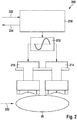
- Figure 1 illustrates a graph 10 showing a hysteresis curve of a typical reactive deposition process.
- This can, for example, be deposition of silicon oxide (SiO2), wherein silicon is sputtered from a cathode while oxygen is provided in the plasma. Thereby, silicon oxide can be deposited on the substrate.
- the curve 12 shown in figure 1 shows the deposition parameters such as the voltage provided to the sputter cathode as a function of the flow of a process gas, such as oxygen.
- a similar hysteresis curve can also be seen for other deposition parameters such as the oxygen content in the plasma, which can for example be measured with a lambda-sensor. Accordingly, the values provided in graph 10 are shown as normalized values.
- curve 12 shows a hysteresis.
- a comparably high cathode voltage is provided and the deposition process is conducted in a metallic mode. Even though a high deposition rate can be provided in the metallic mode, and absorbing layer is deposited, which is not appropriate for a plurality of applications.
- the deposition process turns into an oxygen mode where transparent silicon oxide layer can be deposited. Yet, the deposition rate is comparably low. Accordingly, methods of controlling the reactive deposition process as described herein typically control the deposition process to be provided in a transition mode, where a transparent layer, such as silicon oxide, can be deposited at the comparably high rate.
- Control modes such as current control modes using an oxygen sensor (lambda-sensor) or a plasma monitoring (PEM) require additional hardware for the sensor equipment and control units with fast logic controls to keep the deposition process stable in the transition mode. Signals from such sensors providing information of a plasma characteristic can be fed to fast logic controllers in order to control the power supply or the gas supply. Accordingly, in order to keep the cathode power controlled in the transition mode in the past special monitoring features like PEM or lambda sensors were used in combination with a special control routine. This needs extra hard- and software and is therefore an expensive solution. Further, current control modes are not necessarily beneficial.
- Embodiments described herein provide a closed loop control for the reactive deposition process, wherein the cathode can be power controlled.
- the deposition rate can be constant as the deposition rate is proportional to the power provided to the cathode.
- Embodiments described herein include a voltage supply or a generator that can keep the cathode in transition mode by using a voltage control or an upper voltage limitation.
- the voltage supply results in being voltage controlled and the power is not kept constant, because the power supply can only keep one parameter fixed. If a voltage control is used, the power and therefore the deposition rate is changing with the used process gases (or degassing) and this is not always acceptable. Also a manual deposition rate adjustment is needed if the power supply is operated in voltage mode.
- embodiments described herein provide, in addition to the voltage control of the power supply, a power control as a closed control loop, wherein the actual power is monitored and the flow rate of a process gas is controlled to keep the power essentially constant.
- a closed loop control providing an essentially constant deposition rate can be provided.
- the reactive deposition process such as a SiO 2 process, is voltage controlled or voltage limited and establishes an O 2 flow regulation which keeps the sputter power constant. Thereby, a closed loop control is provided.
- the methods of controlling a reactive deposition process, the closed loop control assemblies configured for a reactive deposition process, and the deposition apparatuses for reactive deposition of a layer on a substrate can be utilized for other reactive deposition processes such as depositing Al 2 O 3 , TiO 2 , ZnO, Nb 2 O 5 , SnO 2 , Si 3 N 4 or the like.
- FIG. 2 shows a closed loop control assembly 200 for illustrating embodiments described herein.
- the control assembly includes a power supply 210.
- the power supply can typically be an AC power supply, such as the middle frequency power supply.
- the oscillating frequency of the power supply can be 1 kHz to 200 kHz.
- the power supply 210 is connected to a cathode assembly.
- the cathode assembly can include a first cathode 214 and the second cathode 215.
- power is provided to a cathode or a cathode assembly, respectively.
- the AC power can be provided to the cathode 214 and the cathode 215 in an alternating manner such that one cathode provides a counter electrode (anode) for the other cathode, respectively, during a half cycle of the AC waveform.
- the power supply 210 can include DC generator and an AC oscillator, such as the middle frequency oscillator.
- the DC generator has a DC power, a DC voltage, and a DC current as output for the oscillator.
- the oscillator has an output power, an output voltage, an output current, and an output frequency provided to the cathode or cathode assembly, respectively.
- the power supply receives a voltage set point signal from a controller. Further, the power supply provides a power value to the controller as indicated by arrow 224. Thereby, typically the power value is the actual AC power, which is provided by the power supply or the oscillator, respectively, to the cathode.
- a process gas is provided in the plasma region of the plasma 20.
- the process gas can include at least one of argon, oxygen, nitrogen, H 2 , H 2 O, and N 2 O.
- oxygen can be provided as a reactive gas for the reactive deposition process. Providing a small amount of nitrogen in the process gas for an oxygen-based reactive process can be beneficial for stabilizing the generated plasma 20.
- the voltage set point value 222 provided as an upper limit for the voltage, which the power supply 210 can provide to the cathode.
- the upper limit can for example have a normalized value of 0.6 to 0.8, for example 0.7.
- the voltage set point value 222 can be set as the limit to keep that deposition process in transition mode.
- the power provided by the power supply thereby depends on the flow of reactive gas in the plasma region 20.
- the power can depend on the oxygen flow while being limited by the voltage set point value.
- the actual power is provided as a signal to a controller as indicated by arrow 224.
- the controller which provides the closed loop control, controls the process gas flow indicated by arrow 232 in dependence of the actual power, which is provided to the cathode.
- the voltage of the power supply is fixed by the set point value and the output power of the power supply 210 is controlled by a controller by means of adjusting the process gas flow.
- the controller can be a programmable logic controller (PLC).
- PLC programmable logic controller
- the process gas flow for example the oxygen flow, is adjusted to keep the output power and, thereby, the deposition rate constant, constant deposition rate can be provided in transition mode without having additional hardware like lambda-sensors or plasma monitoring (PEM).
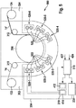
- Figure 3 illustrates a deposition apparatus 300 including the closed loop control assembly.
- the deposition apparatus 300 shown in figure 3 includes a power supply 210.
- the AC power supply is connected to the rotatable cathode 314 and the chamber 32 of the deposition apparatus 300.
- the AC power supply can be connected to one cathode and a counter electrode provided by the housing, by another part of the deposition apparatus, or by another electrode.
- the other electrode can be provided on the side of the substrate opposing the cathode 314.
- a cathode assembly with two cathodes can be provided, wherein the AC power supply is connected to the first and the second cathode in order to provide a twin-cathode-assembly which is driven by an alternating power. Typically, middle frequency power is applied.
- the cathodes can be magnetron sputtering cathodes.
- planar cathodes as shown in figure 2 or rotational cathodes as shown in figures 3 and 5 can be utilized for the reactive deposition process as described herein, the respective control assemblies and deposition apparatuses.
- the cathodes 214, 215 and 314, as well as the other cathode referred to herein can be either a cathode or an anode when AC power is supplied.
- the sputtering targets are referred to as cathodes even though there function can be the function of an anode during a half cycle of the AC frequency waveform.
- the voltage set point 222 is provided by the controller 310 and the controller 310 receives the power value, which is typically the actually provided MF power which is output to the cathode 314.
- the controller 310 provides the signal 232 to the gas supply 310 including a gas conduit 334 for providing process gas in the chamber 32.
- the substrate 30 is transported through the chamber 32 for reactive deposition of the layer, for example, silicon oxide, aluminum oxide, TiO 2 , ZnO, Nb 2 O 5 , SnO 2 , Si 3 N 4 or the like.
- the gas flow rate provided by conduit 334 in the plasma region in the chamber 32 is proportional to the output power of the power supply 210 provided to the cathode 314.
- the controller 310 controls the gas flow rate such that the actual power value 224, which is provided as a signal from the power supply to the controller 310, is essentially constant. Thereby a closed loop control is established.
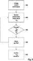
- Figure 4 illustrates yet another embodiment of a closed loop control assembly for powering cathodes 214 and 215.
- the closed loop control and the method of operating the closed loop control is described with respect to figures 4 and 6 .
- a set point voltage and a set point power can be provided to the controller 310. This can for example be done through the graphical user interface by an operator.
- the set point voltage can be a DC voltage and the set point power can be the middle frequency power.
- the set point voltage can also be the middle frequency voltage and the set point power might also be a DC power, which is outputted from a DC generator to oscillator in the power supply.
- the controller 310 provides the set point voltage as indicated by arrow 222 to the power supply 210.
- the power supply 210 can include a DC generator 412 and an AC oscillator, for example, a middle frequency oscillator 414.
- the power supply 210 is configured for using the voltage set point 222 as the desired output voltage, particularly as an upper voltage limit of the voltage provided by the power supply 210.
- the set point voltage is a DC voltage
- the power supply 210 can use the set point as an upper limit of the DC voltage provided by the DC generator 412 to the oscillator 414.
- the set point voltage is a MF voltage
- the power supply 210 can use the set point as an upper limit of the MF voltage provided by the oscillator 414 to the cathodes.
- the power supply is operated voltage controlled as shown in step 602 in figure 6 .
- the voltage set point 422 is provided such that the deposition process is conducted in transition mode.
- the transition mode can be stabilized and the actual AC power provided by the oscillator 414 to the cathodes 214 and 215 depends on the process gas available in the plasma region.
- the actual power provided to the cathodes 214 and 215 is provided as a signal 224 from, for example, the oscillator to the controller 310. This corresponds to step 604 in figure 6 where the actual power Pact is received.
- the controller compares the actual power Pact to the set point power 424 in step 606.
- the gas flow of the process gas, and particularly that gas flow of the reactive gas being included in the process gas is adjusted.
- the oxygen flow can be adjusted within certain limits and can be adjusted by a predetermined increment.
- the closed loop control is implemented to provide an essentially constant power.
- an essentially constant deposition rate is provided in the transition mode, which is set by the voltage control of the power supply.
- Figure 6 illustrates a further step 610, which can be provided according to some optional modifications of embodiments described herein.
- the actual power 224 which is provided as a signal from the power supply 210 to the controller 310
- the actual voltage is provided as a signal from the power supply 210 to the controller 310.
- the actual voltage is monitored. If the actual voltage drops below the lower limit, oxygen mode is detected. This can be understood with respect to figure 1 . If the normalized voltage would drop to the value of below 0.4, the reactive deposition process would be in the oxygen mode as shown in figure 1 .
- the oxygen flow rate can be set to the minimum oxygen set point level in order to return via the metallic mode in the transition mode for the deposition process.
- Fig. 5 schematically illustrates an example of a deposition apparatus 500 for reactive deposition of a layer on a substrate, e.g. a flexible substrate, according to embodiments herein.
- the deposition apparatus 500 may include an unwind roller 132 and a rewind roller 134 for unwinding of substrate 14 prior to deposition and winding of substrate 14.
- Deposition apparatus 500 may include a roller system (not shown) for translation of substrate 14 through the different processing chambers.
- a deposition apparatus according to embodiments herein may be constituted as a sputter roll coater for roll-to-roll deposition on a plastic film.
- the processing module of apparatus 500 can further include rollers 310, 312 for appropriately feeding a substrate 14 to processing drum 306, and facilitating feeding of a processed substrate 14' from process module to winding module 304.
- Deposition apparatus 500 may be a SmartWebTM, manufactured by Applied Materials, adapted for manufacturing a transparent body according to embodiments of the present disclosure. Examples of a roll-to-roll deposition apparatus, which could be adapted according to embodiments herein, are described in European patent application Appl. No. EP20040003574 , entitled "Strip coating installation with a vacuum chamber and a coating cylinder" filed February 18, 2004 and published under publication number EP 1 561 837 A1 , which is incorporated herein by reference to the extent the application is not inconsistent with this disclosure.
- the exemplarily apparatus shown in Fig. 5 includes a first deposition assembly having five target assemblies 520-1 to 520-6 and configured to deposit a layer or layer stack over a substrate 14.
- a first deposition assembly having five target assemblies 520-1 to 520-6 and configured to deposit a layer or layer stack over a substrate 14.
- each several layers of a layer stack can deposited in an individual deposition chamber or individual compartments of a deposition chamber.
- each compartment can be used to deposit further material of the same layer.
- the apparatus 500 can include 6 compartments, chambers or sub-chambers, such that each compartment can be operated under individual processing parameters, particularly with individual processing gases.
- the apparatus can include six rotatable MF cathodes or target assemblies 520-1 to 520-6 equipped with Si targets, e.g. sprayed Si target tubes 522.
- the controller 310, the power supply 219 having e.g. a DC generator 412 and an MF oscillator 414, the gas supply 330, and the gas conduit 334 are only shown for the first target assembly 520-1.
- power supplies and gas supplies can be provided for each of the compartments of the deposition apparatus and a controller 310 can be used to control deposition in each department.
- a controller such as PLC, can be provided for each deposition process.
- a common user interface can be provided to provide set point voltages and set point powers for each deposition zone.
- similar set point voltages and set point powers can be provided for two or more, or even all deposition zones.
- one or a few of the deposition assemblies 520-1 to 520-6 can be provided for a reactive deposition process and with a closed loop control assembly according to embodiments described herein.
- a three-layer transparent layer stack having three silicon-containing dielectric films can be manufactured with the closed loop control according to embodiments described herein. Thereby, a lambda-sensor or PEM can be avoided for one or more of the deposition compartments.
- the apparatus 500 shown in Fig. 5 and having 6 compartments, target assemblies or cathodes can also be further scaled up, e.g. to 8 10 or even 12 compartments, target assemblies or cathodes.
- at least the throughput can be further increased by such an up scaling, because the layer limiting the speed of the substrate based upon layer thickness and/or deposition rate can be deposited with an additional cathode.
- a set point voltage 422 and a set point power 424 can be provided to the controller 310.
- the controller 310 provides the set point voltage to the power supply 210.
- the power supply 210 can include a DC generator 412 and an AC oscillator, for example, a middle frequency oscillator 414.
- the power supply is operated voltage controlled such that the deposition process is conducted in transition mode. Thereby, due to the upper voltage limit, the transition mode can be stabilized and the actual AC power provided by the oscillator 414 to the cathodes 214 and 215 depends on the process gas available provided by gas supply 330 to conduit 334.
- the actual power provided to the cathodes 522 is provided as a signal to the controller 310.
- the gas flow of the process gas is adjusted in dependence of the actual power.
- the MF Generator is P MF -controlled, or U MF controlled.
- the power control of the generator or the process as such can be utilized by the closed loop control of the flow rate of the process gas as the voltage limit is typically not reached.
- a P MF set point provided to the power supply can be set about 10% higher than the requested process P MF-Set set point.
- the U DC/MF limit set point will be changed to the process required set point U DC/MF-Set .
- the Oxygen Flow will be changed depending on the difference of the requested MF-Power (PMF-Set) and actual MF-Power (PMF-Act). If PMF-Act is smaller than PMF-Set the gas flow, e.g. the oxygen flow, is increased. If PMF-Act is larger than PMF-Set gas flow, e.g. the oxygen flow, is decreased.
- the gas flow e.g. the oxygen flow
- the gas flow can be changed within limits (FlowMinLimit and FlowMaxLimit) by deltaFlow per min.
- FlowMinLimit and FlowMaxLimit limits
- FlowMaxLimit limits
- UDC/MF-Act actual voltage
- UDC/MF-Set set point Voltage
- the apparatus including the closed loop control assembly and the method of reactive layer deposition as described herein, there is no need for additional hardware like PEM or lambda sensors. Yet, a stable deposition rate in transition mode, i.e. with sufficient deposition rate, can be provided.
Landscapes
- Chemical & Material Sciences (AREA)
- Engineering & Computer Science (AREA)
- Mechanical Engineering (AREA)
- Chemical Kinetics & Catalysis (AREA)
- Materials Engineering (AREA)
- Metallurgy (AREA)
- Organic Chemistry (AREA)
- Physics & Mathematics (AREA)
- Plasma & Fusion (AREA)
- Analytical Chemistry (AREA)
- Fluid Mechanics (AREA)
- Physical Vapour Deposition (AREA)
- Plasma Technology (AREA)
- Physical Or Chemical Processes And Apparatus (AREA)
- Chemical Vapour Deposition (AREA)
Applications Claiming Priority (1)
| Application Number | Priority Date | Filing Date | Title |
|---|---|---|---|
| PCT/EP2011/071425 WO2013079108A1 (en) | 2011-11-30 | 2011-11-30 | Closed loop control |
Publications (2)
| Publication Number | Publication Date |
|---|---|
| EP2785892A1 EP2785892A1 (en) | 2014-10-08 |
| EP2785892B1 true EP2785892B1 (en) | 2017-09-27 |
Family
ID=45349469
Family Applications (1)
| Application Number | Title | Priority Date | Filing Date |
|---|---|---|---|
| EP11796945.1A Revoked EP2785892B1 (en) | 2011-11-30 | 2011-11-30 | Closed loop control |
Country Status (7)
| Country | Link |
|---|---|
| US (1) | US9758855B2 (enExample) |
| EP (1) | EP2785892B1 (enExample) |
| JP (1) | JP6305929B2 (enExample) |
| KR (2) | KR20180132975A (enExample) |
| CN (1) | CN103958723B (enExample) |
| TW (1) | TWI592510B (enExample) |
| WO (1) | WO2013079108A1 (enExample) |
Families Citing this family (10)
| Publication number | Priority date | Publication date | Assignee | Title |
|---|---|---|---|---|
| EA020763B9 (ru) | 2008-08-04 | 2015-05-29 | Эй-Джи-Си Флет Гласс Норт Эмерике, Инк. | Источник плазмы и способы нанесения тонкопленочных покрытий с использованием плазменно-химического осаждения из газовой фазы |
| WO2016034197A1 (en) * | 2014-09-01 | 2016-03-10 | Applied Materials, Inc. | Assembly and method for deposition of material on a substrate |
| BR112017011612A2 (pt) | 2014-12-05 | 2018-01-16 | Agc Glass Europe, S.A | fonte de plasma de cátodo oco |
| EP3228161B1 (en) | 2014-12-05 | 2021-11-03 | AGC Flat Glass North America, Inc. | Plasma source utilizing a macro-particle reduction coating and method of using a plasma source utilizing a macro-particle reduction coating for deposition of thin film coatings and modification of surfaces |
| US9721765B2 (en) * | 2015-11-16 | 2017-08-01 | Agc Flat Glass North America, Inc. | Plasma device driven by multiple-phase alternating or pulsed electrical current |
| US10573499B2 (en) | 2015-12-18 | 2020-02-25 | Agc Flat Glass North America, Inc. | Method of extracting and accelerating ions |
| US10242846B2 (en) | 2015-12-18 | 2019-03-26 | Agc Flat Glass North America, Inc. | Hollow cathode ion source |
| DE102016116762B4 (de) * | 2016-09-07 | 2021-11-11 | Fraunhofer-Gesellschaft zur Förderung der angewandten Forschung e.V. | Verfahren zum Abscheiden einer Schicht mittels einer Magnetronsputtereinrichtung |
| KR102643656B1 (ko) | 2017-11-09 | 2024-03-05 | 어플라이드 머티어리얼스, 인코포레이티드 | 리튬 금속 애노드에 대해 칼코게나이드들을 사용하는 엑스-시튜 고체 전해질 계면 개질 |
| US11631840B2 (en) | 2019-04-26 | 2023-04-18 | Applied Materials, Inc. | Surface protection of lithium metal anode |
Citations (7)
| Publication number | Priority date | Publication date | Assignee | Title |
|---|---|---|---|---|
| GB2021294A (en) | 1978-05-13 | 1979-11-28 | Leybold Heraeus Gmbh & Co Kg | Method and arrangement for regulating the discharge process in a cathode sputtering apparatus |
| US4201645A (en) | 1978-06-26 | 1980-05-06 | Robert J. Ferran | Closed-loop sputtering system and method of operating same |
| DE4106513A1 (de) | 1991-03-01 | 1992-09-03 | Leybold Ag | Verfahren zur regelung eines reaktiven sputterprozesses und vorrichtung zur durchfuehrung des verfahrens |
| WO2000028104A1 (en) | 1998-11-06 | 2000-05-18 | Scivac | Sputtering apparatus and process for high rate coatings |
| US6106676A (en) | 1998-04-16 | 2000-08-22 | The Boc Group, Inc. | Method and apparatus for reactive sputtering employing two control loops |
| EP1553206A1 (en) | 2002-05-29 | 2005-07-13 | Kabushiki Kaisha Kobe Seiko Sho | Reactive sputtering method and device |
| DE102009053756B4 (de) | 2009-06-26 | 2011-07-21 | VON ARDENNE Anlagentechnik GmbH, 01324 | Verfahren zur Beschichtung eines Substrates in einer Vakuumkammer mit mindestens einem rotierenden Magnetron |
Family Cites Families (3)
| Publication number | Priority date | Publication date | Assignee | Title |
|---|---|---|---|---|
| US6537428B1 (en) * | 1999-09-02 | 2003-03-25 | Veeco Instruments, Inc. | Stable high rate reactive sputtering |
| DE102004006131B4 (de) | 2004-02-07 | 2005-12-15 | Applied Films Gmbh & Co. Kg | Bandbeschichtungsanlage mit einer Vakuumkammer und einer Beschichtungswalze |
| JP2010229523A (ja) * | 2009-03-27 | 2010-10-14 | Bridgestone Corp | 導電性透明化合物薄膜の成膜方法および導電性透明化合物薄膜 |
-
2011
- 2011-11-30 JP JP2014543775A patent/JP6305929B2/ja active Active
- 2011-11-30 EP EP11796945.1A patent/EP2785892B1/en not_active Revoked
- 2011-11-30 CN CN201180075166.4A patent/CN103958723B/zh active Active
- 2011-11-30 US US14/357,168 patent/US9758855B2/en not_active Expired - Fee Related
- 2011-11-30 WO PCT/EP2011/071425 patent/WO2013079108A1/en not_active Ceased
- 2011-11-30 KR KR1020187035066A patent/KR20180132975A/ko not_active Ceased
- 2011-11-30 KR KR1020147017890A patent/KR20140097510A/ko not_active Ceased
-
2012
- 2012-11-29 TW TW101144735A patent/TWI592510B/zh active
Patent Citations (8)
| Publication number | Priority date | Publication date | Assignee | Title |
|---|---|---|---|---|
| GB2021294A (en) | 1978-05-13 | 1979-11-28 | Leybold Heraeus Gmbh & Co Kg | Method and arrangement for regulating the discharge process in a cathode sputtering apparatus |
| US4201645A (en) | 1978-06-26 | 1980-05-06 | Robert J. Ferran | Closed-loop sputtering system and method of operating same |
| DE4106513A1 (de) | 1991-03-01 | 1992-09-03 | Leybold Ag | Verfahren zur regelung eines reaktiven sputterprozesses und vorrichtung zur durchfuehrung des verfahrens |
| US5556520A (en) | 1991-03-01 | 1996-09-17 | Leybold Aktiengesellschaft | Method for controlling a reactive sputtering process |
| US6106676A (en) | 1998-04-16 | 2000-08-22 | The Boc Group, Inc. | Method and apparatus for reactive sputtering employing two control loops |
| WO2000028104A1 (en) | 1998-11-06 | 2000-05-18 | Scivac | Sputtering apparatus and process for high rate coatings |
| EP1553206A1 (en) | 2002-05-29 | 2005-07-13 | Kabushiki Kaisha Kobe Seiko Sho | Reactive sputtering method and device |
| DE102009053756B4 (de) | 2009-06-26 | 2011-07-21 | VON ARDENNE Anlagentechnik GmbH, 01324 | Verfahren zur Beschichtung eines Substrates in einer Vakuumkammer mit mindestens einem rotierenden Magnetron |
Non-Patent Citations (9)
| Title |
|---|
| "Operating instructions TruPlasma MF 7025 - 7100 (A 05- 0124-00.BEN-001-08)", TRUMPF, 5 May 2009 (2009-05-05), pages 1 - 174, XP055510541 |
| BELLIDO-GONZÄLEZ ET AL.: "Flexible Gas Control for Reactive Magnetron Sputtering Process", PROCEEDINGS OF AIMCAL, October 2004 (2004-10-01), Charleston USA, pages 1 - 8, XP055510529 |
| GRUBER C. ET AL.: "Voltage Control for Reactive Sputtering: Improving Typical Sputter Rate while Dramatically Reducing Input Power Requirements", 52ND ANNUAL TECHNICAL CONFERENCE PROCEEDINGS, 9 May 2009 (2009-05-09), Santa Clara, CA, pages 153 - 157, XP055510512, ISSN: 0737-5921 |
| KAZUSS J. ET AL.: "Control of Reactive Deposition Process by Stabilization of the Power Supply Work", 54TH ANNUAL TECHNICAL CONFERENCE PROCEEDINGS, 16 April 2011 (2011-04-16), Chicago, IL, pages 419 - 422, XP055510500, ISSN: 0737-5921 |
| KON ET AL.: "Impedance Control of Reactive Sputtering Process in Mid-Frequency Mode with Dual Cathodes to Deposit Al-Doped ZnO Films", JAPANESE JOURNAL OF APPLIED PHYSICS, vol. 42, no. 1, January 2003 (2003-01-01), pages 263 - 269, XP055510539 |
| KOSKI K. ET AL.: "Voltage controlled reactive sputtering process for aluminium oxide thin films", THIN SOLID FILMS, vol. 326, no. 1-2, 4 August 1998 (1998-08-04), pages 189 - 193, XP004141482 |
| LINSS ET AL.: "ZnO:Al for CIGS Solar Modules Deposited by Reactive Sputtering from Rotatable Magnetron", 54TH ANNUAL TECHNICAL CONFERENCE PROCEEDINGS, 16 April 2011 (2011-04-16), Chicago, IL, pages 508 - 513, XP055510525, ISSN: 0737-5921 |
| MAY ET AL.: "ITO coating by reactive magnetron sputtering- comparison of properties from DC and MF processing", THIN SOLID FILMS, vol. 351, no. 1, 30 August 1999 (1999-08-30), pages 48 - 52, XP085016937 |
| RUSKE ET AL.: "Properties of Sn02 films prepared by DC and MF reactive sputtering", THIN SOLID FILMS, vol. 351, no. 1-2, 1999, pages 146 - 150, XP085016917 |
Also Published As
| Publication number | Publication date |
|---|---|
| JP6305929B2 (ja) | 2018-04-04 |
| KR20140097510A (ko) | 2014-08-06 |
| CN103958723A (zh) | 2014-07-30 |
| JP2015500921A (ja) | 2015-01-08 |
| US20150152542A1 (en) | 2015-06-04 |
| WO2013079108A1 (en) | 2013-06-06 |
| CN103958723B (zh) | 2017-04-05 |
| TWI592510B (zh) | 2017-07-21 |
| KR20180132975A (ko) | 2018-12-12 |
| TW201329279A (zh) | 2013-07-16 |
| EP2785892A1 (en) | 2014-10-08 |
| US9758855B2 (en) | 2017-09-12 |
Similar Documents
| Publication | Publication Date | Title |
|---|---|---|
| EP2785892B1 (en) | Closed loop control | |
| US11680322B2 (en) | Method for forming a laminated film on a substrate | |
| US8658001B2 (en) | Method and control system for depositing a layer | |
| JP2006249471A (ja) | 成膜方法 | |
| JP6596474B2 (ja) | 閉ループ制御 | |
| US8992742B2 (en) | Method for coating a substrate in a vacuum chamber having a rotating magnetron | |
| US6783640B2 (en) | Sputtering method and sputtering apparatus | |
| US20180135160A1 (en) | Method for controlling a gas supply to a process chamber, controller for controlling a gas supply to a process chamber, and apparatus | |
| Strümpfel et al. | Reactive dual magnetron sputtering of oxides for large area production of optical multilayers | |
| JP7572997B2 (ja) | 真空処理装置及び真空処理方法 | |
| WO2016034197A1 (en) | Assembly and method for deposition of material on a substrate | |
| JP2006249473A (ja) | 成膜方法および成膜装置 | |
| WO2019154490A1 (en) | Deposition apparatus, method of coating a flexible substrate and flexible substrate having a coating | |
| US20250305119A1 (en) | Method of manufacturing gas barrier film | |
| JP2015074790A (ja) | プラズマ処理装置および処理方法 | |
| CN107916406B (zh) | 用于双极磁控溅射的方法和磁控装置 | |
| WO2007099780A1 (ja) | スパッタリング装置およびその成膜方法 | |
| JP2010007113A (ja) | 成膜方法および成膜装置 |
Legal Events
| Date | Code | Title | Description |
|---|---|---|---|
| PUAI | Public reference made under article 153(3) epc to a published international application that has entered the european phase |
Free format text: ORIGINAL CODE: 0009012 |
|
| 17P | Request for examination filed |
Effective date: 20140613 |
|
| AK | Designated contracting states |
Kind code of ref document: A1 Designated state(s): AL AT BE BG CH CY CZ DE DK EE ES FI FR GB GR HR HU IE IS IT LI LT LU LV MC MK MT NL NO PL PT RO RS SE SI SK SM TR |
|
| DAX | Request for extension of the european patent (deleted) | ||
| REG | Reference to a national code |
Ref country code: DE Ref legal event code: R079 Ref document number: 602011041971 Country of ref document: DE Free format text: PREVIOUS MAIN CLASS: C23C0014000000 Ipc: C23C0014560000 |
|
| GRAP | Despatch of communication of intention to grant a patent |
Free format text: ORIGINAL CODE: EPIDOSNIGR1 |
|
| RIC1 | Information provided on ipc code assigned before grant |
Ipc: H01J 37/34 20060101ALI20170321BHEP Ipc: C23C 14/56 20060101AFI20170321BHEP |
|
| INTG | Intention to grant announced |
Effective date: 20170412 |
|
| GRAS | Grant fee paid |
Free format text: ORIGINAL CODE: EPIDOSNIGR3 |
|
| GRAA | (expected) grant |
Free format text: ORIGINAL CODE: 0009210 |
|
| AK | Designated contracting states |
Kind code of ref document: B1 Designated state(s): AL AT BE BG CH CY CZ DE DK EE ES FI FR GB GR HR HU IE IS IT LI LT LU LV MC MK MT NL NO PL PT RO RS SE SI SK SM TR |
|
| REG | Reference to a national code |
Ref country code: GB Ref legal event code: FG4D |
|
| REG | Reference to a national code |
Ref country code: CH Ref legal event code: EP |
|
| REG | Reference to a national code |
Ref country code: AT Ref legal event code: REF Ref document number: 932041 Country of ref document: AT Kind code of ref document: T Effective date: 20171015 |
|
| REG | Reference to a national code |
Ref country code: IE Ref legal event code: FG4D |
|
| REG | Reference to a national code |
Ref country code: DE Ref legal event code: R096 Ref document number: 602011041971 Country of ref document: DE |
|
| REG | Reference to a national code |
Ref country code: CH Ref legal event code: NV Representative=s name: MICHELI AND CIE SA, CH |
|
| PG25 | Lapsed in a contracting state [announced via postgrant information from national office to epo] |
Ref country code: NO Free format text: LAPSE BECAUSE OF FAILURE TO SUBMIT A TRANSLATION OF THE DESCRIPTION OR TO PAY THE FEE WITHIN THE PRESCRIBED TIME-LIMIT Effective date: 20171227 Ref country code: FI Free format text: LAPSE BECAUSE OF FAILURE TO SUBMIT A TRANSLATION OF THE DESCRIPTION OR TO PAY THE FEE WITHIN THE PRESCRIBED TIME-LIMIT Effective date: 20170927 Ref country code: LT Free format text: LAPSE BECAUSE OF FAILURE TO SUBMIT A TRANSLATION OF THE DESCRIPTION OR TO PAY THE FEE WITHIN THE PRESCRIBED TIME-LIMIT Effective date: 20170927 Ref country code: HR Free format text: LAPSE BECAUSE OF FAILURE TO SUBMIT A TRANSLATION OF THE DESCRIPTION OR TO PAY THE FEE WITHIN THE PRESCRIBED TIME-LIMIT Effective date: 20170927 Ref country code: SE Free format text: LAPSE BECAUSE OF FAILURE TO SUBMIT A TRANSLATION OF THE DESCRIPTION OR TO PAY THE FEE WITHIN THE PRESCRIBED TIME-LIMIT Effective date: 20170927 |
|
| REG | Reference to a national code |
Ref country code: NL Ref legal event code: MP Effective date: 20170927 |
|
| REG | Reference to a national code |
Ref country code: LT Ref legal event code: MG4D |
|
| REG | Reference to a national code |
Ref country code: AT Ref legal event code: MK05 Ref document number: 932041 Country of ref document: AT Kind code of ref document: T Effective date: 20170927 |
|
| PG25 | Lapsed in a contracting state [announced via postgrant information from national office to epo] |
Ref country code: RS Free format text: LAPSE BECAUSE OF FAILURE TO SUBMIT A TRANSLATION OF THE DESCRIPTION OR TO PAY THE FEE WITHIN THE PRESCRIBED TIME-LIMIT Effective date: 20170927 Ref country code: LV Free format text: LAPSE BECAUSE OF FAILURE TO SUBMIT A TRANSLATION OF THE DESCRIPTION OR TO PAY THE FEE WITHIN THE PRESCRIBED TIME-LIMIT Effective date: 20170927 Ref country code: GR Free format text: LAPSE BECAUSE OF FAILURE TO SUBMIT A TRANSLATION OF THE DESCRIPTION OR TO PAY THE FEE WITHIN THE PRESCRIBED TIME-LIMIT Effective date: 20171228 Ref country code: BG Free format text: LAPSE BECAUSE OF FAILURE TO SUBMIT A TRANSLATION OF THE DESCRIPTION OR TO PAY THE FEE WITHIN THE PRESCRIBED TIME-LIMIT Effective date: 20171227 |
|
| PG25 | Lapsed in a contracting state [announced via postgrant information from national office to epo] |
Ref country code: NL Free format text: LAPSE BECAUSE OF FAILURE TO SUBMIT A TRANSLATION OF THE DESCRIPTION OR TO PAY THE FEE WITHIN THE PRESCRIBED TIME-LIMIT Effective date: 20170927 |
|
| PG25 | Lapsed in a contracting state [announced via postgrant information from national office to epo] |
Ref country code: CZ Free format text: LAPSE BECAUSE OF FAILURE TO SUBMIT A TRANSLATION OF THE DESCRIPTION OR TO PAY THE FEE WITHIN THE PRESCRIBED TIME-LIMIT Effective date: 20170927 Ref country code: ES Free format text: LAPSE BECAUSE OF FAILURE TO SUBMIT A TRANSLATION OF THE DESCRIPTION OR TO PAY THE FEE WITHIN THE PRESCRIBED TIME-LIMIT Effective date: 20170927 Ref country code: RO Free format text: LAPSE BECAUSE OF FAILURE TO SUBMIT A TRANSLATION OF THE DESCRIPTION OR TO PAY THE FEE WITHIN THE PRESCRIBED TIME-LIMIT Effective date: 20170927 |
|
| PG25 | Lapsed in a contracting state [announced via postgrant information from national office to epo] |
Ref country code: SM Free format text: LAPSE BECAUSE OF FAILURE TO SUBMIT A TRANSLATION OF THE DESCRIPTION OR TO PAY THE FEE WITHIN THE PRESCRIBED TIME-LIMIT Effective date: 20170927 Ref country code: SK Free format text: LAPSE BECAUSE OF FAILURE TO SUBMIT A TRANSLATION OF THE DESCRIPTION OR TO PAY THE FEE WITHIN THE PRESCRIBED TIME-LIMIT Effective date: 20170927 Ref country code: EE Free format text: LAPSE BECAUSE OF FAILURE TO SUBMIT A TRANSLATION OF THE DESCRIPTION OR TO PAY THE FEE WITHIN THE PRESCRIBED TIME-LIMIT Effective date: 20170927 Ref country code: AT Free format text: LAPSE BECAUSE OF FAILURE TO SUBMIT A TRANSLATION OF THE DESCRIPTION OR TO PAY THE FEE WITHIN THE PRESCRIBED TIME-LIMIT Effective date: 20170927 Ref country code: IS Free format text: LAPSE BECAUSE OF FAILURE TO SUBMIT A TRANSLATION OF THE DESCRIPTION OR TO PAY THE FEE WITHIN THE PRESCRIBED TIME-LIMIT Effective date: 20180127 Ref country code: IT Free format text: LAPSE BECAUSE OF FAILURE TO SUBMIT A TRANSLATION OF THE DESCRIPTION OR TO PAY THE FEE WITHIN THE PRESCRIBED TIME-LIMIT Effective date: 20170927 |
|
| REG | Reference to a national code |
Ref country code: DE Ref legal event code: R026 Ref document number: 602011041971 Country of ref document: DE |
|
| PG25 | Lapsed in a contracting state [announced via postgrant information from national office to epo] |
Ref country code: MC Free format text: LAPSE BECAUSE OF FAILURE TO SUBMIT A TRANSLATION OF THE DESCRIPTION OR TO PAY THE FEE WITHIN THE PRESCRIBED TIME-LIMIT Effective date: 20170927 |
|
| PLBI | Opposition filed |
Free format text: ORIGINAL CODE: 0009260 |
|
| PLAX | Notice of opposition and request to file observation + time limit sent |
Free format text: ORIGINAL CODE: EPIDOSNOBS2 |
|
| PG25 | Lapsed in a contracting state [announced via postgrant information from national office to epo] |
Ref country code: DK Free format text: LAPSE BECAUSE OF FAILURE TO SUBMIT A TRANSLATION OF THE DESCRIPTION OR TO PAY THE FEE WITHIN THE PRESCRIBED TIME-LIMIT Effective date: 20170927 |
|
| 26 | Opposition filed |
Opponent name: VON ARDENNE GMBH Effective date: 20180627 |
|
| PG25 | Lapsed in a contracting state [announced via postgrant information from national office to epo] |
Ref country code: PL Free format text: LAPSE BECAUSE OF FAILURE TO SUBMIT A TRANSLATION OF THE DESCRIPTION OR TO PAY THE FEE WITHIN THE PRESCRIBED TIME-LIMIT Effective date: 20170927 Ref country code: LU Free format text: LAPSE BECAUSE OF NON-PAYMENT OF DUE FEES Effective date: 20171130 |
|
| REG | Reference to a national code |
Ref country code: FR Ref legal event code: ST Effective date: 20180731 Ref country code: BE Ref legal event code: MM Effective date: 20171130 |
|
| REG | Reference to a national code |
Ref country code: IE Ref legal event code: MM4A |
|
| PG25 | Lapsed in a contracting state [announced via postgrant information from national office to epo] |
Ref country code: MT Free format text: LAPSE BECAUSE OF NON-PAYMENT OF DUE FEES Effective date: 20171130 |
|
| PG25 | Lapsed in a contracting state [announced via postgrant information from national office to epo] |
Ref country code: IE Free format text: LAPSE BECAUSE OF NON-PAYMENT OF DUE FEES Effective date: 20171130 Ref country code: FR Free format text: LAPSE BECAUSE OF NON-PAYMENT OF DUE FEES Effective date: 20171130 |
|
| PLBB | Reply of patent proprietor to notice(s) of opposition received |
Free format text: ORIGINAL CODE: EPIDOSNOBS3 |
|
| PG25 | Lapsed in a contracting state [announced via postgrant information from national office to epo] |
Ref country code: BE Free format text: LAPSE BECAUSE OF NON-PAYMENT OF DUE FEES Effective date: 20171130 Ref country code: SI Free format text: LAPSE BECAUSE OF FAILURE TO SUBMIT A TRANSLATION OF THE DESCRIPTION OR TO PAY THE FEE WITHIN THE PRESCRIBED TIME-LIMIT Effective date: 20170927 |
|
| PG25 | Lapsed in a contracting state [announced via postgrant information from national office to epo] |
Ref country code: HU Free format text: LAPSE BECAUSE OF FAILURE TO SUBMIT A TRANSLATION OF THE DESCRIPTION OR TO PAY THE FEE WITHIN THE PRESCRIBED TIME-LIMIT; INVALID AB INITIO Effective date: 20111130 |
|
| PG25 | Lapsed in a contracting state [announced via postgrant information from national office to epo] |
Ref country code: CY Free format text: LAPSE BECAUSE OF FAILURE TO SUBMIT A TRANSLATION OF THE DESCRIPTION OR TO PAY THE FEE WITHIN THE PRESCRIBED TIME-LIMIT Effective date: 20170927 |
|
| REG | Reference to a national code |
Ref country code: DE Ref legal event code: R064 Ref document number: 602011041971 Country of ref document: DE Ref country code: DE Ref legal event code: R103 Ref document number: 602011041971 Country of ref document: DE |
|
| PG25 | Lapsed in a contracting state [announced via postgrant information from national office to epo] |
Ref country code: MK Free format text: LAPSE BECAUSE OF FAILURE TO SUBMIT A TRANSLATION OF THE DESCRIPTION OR TO PAY THE FEE WITHIN THE PRESCRIBED TIME-LIMIT Effective date: 20170927 |
|
| RDAF | Communication despatched that patent is revoked |
Free format text: ORIGINAL CODE: EPIDOSNREV1 |
|
| PGFP | Annual fee paid to national office [announced via postgrant information from national office to epo] |
Ref country code: DE Payment date: 20191121 Year of fee payment: 9 |
|
| PG25 | Lapsed in a contracting state [announced via postgrant information from national office to epo] |
Ref country code: TR Free format text: LAPSE BECAUSE OF FAILURE TO SUBMIT A TRANSLATION OF THE DESCRIPTION OR TO PAY THE FEE WITHIN THE PRESCRIBED TIME-LIMIT Effective date: 20170927 |
|
| PGFP | Annual fee paid to national office [announced via postgrant information from national office to epo] |
Ref country code: CH Payment date: 20191121 Year of fee payment: 9 |
|
| PGFP | Annual fee paid to national office [announced via postgrant information from national office to epo] |
Ref country code: GB Payment date: 20191120 Year of fee payment: 9 |
|
| PG25 | Lapsed in a contracting state [announced via postgrant information from national office to epo] |
Ref country code: PT Free format text: LAPSE BECAUSE OF FAILURE TO SUBMIT A TRANSLATION OF THE DESCRIPTION OR TO PAY THE FEE WITHIN THE PRESCRIBED TIME-LIMIT Effective date: 20170927 |
|
| RDAG | Patent revoked |
Free format text: ORIGINAL CODE: 0009271 |
|
| STAA | Information on the status of an ep patent application or granted ep patent |
Free format text: STATUS: PATENT REVOKED |
|
| PG25 | Lapsed in a contracting state [announced via postgrant information from national office to epo] |
Ref country code: AL Free format text: LAPSE BECAUSE OF FAILURE TO SUBMIT A TRANSLATION OF THE DESCRIPTION OR TO PAY THE FEE WITHIN THE PRESCRIBED TIME-LIMIT Effective date: 20170927 |
|
| REG | Reference to a national code |
Ref country code: CH Ref legal event code: PL |
|
| REG | Reference to a national code |
Ref country code: FI Ref legal event code: MGE |
|
| 27W | Patent revoked |
Effective date: 20191119 |
|
| GBPR | Gb: patent revoked under art. 102 of the ep convention designating the uk as contracting state |
Effective date: 20191119 |