EP2777065B1 - Procédé d'essai de conservation de données d'une cellule de mémoire non volatile ayant une grille flottante - Google Patents
Procédé d'essai de conservation de données d'une cellule de mémoire non volatile ayant une grille flottante Download PDFInfo
- Publication number
- EP2777065B1 EP2777065B1 EP12848380.7A EP12848380A EP2777065B1 EP 2777065 B1 EP2777065 B1 EP 2777065B1 EP 12848380 A EP12848380 A EP 12848380A EP 2777065 B1 EP2777065 B1 EP 2777065B1
- Authority
- EP
- European Patent Office
- Prior art keywords
- floating gate
- memory cell
- voltage
- gate
- region
- Prior art date
- Legal status (The legal status is an assumption and is not a legal conclusion. Google has not performed a legal analysis and makes no representation as to the accuracy of the status listed.)
- Active
Links
Images
Classifications
-
- G—PHYSICS
- G11—INFORMATION STORAGE
- G11C—STATIC STORES
- G11C29/00—Checking stores for correct operation ; Subsequent repair; Testing stores during standby or offline operation
- G11C29/04—Detection or location of defective memory elements, e.g. cell constructio details, timing of test signals
- G11C29/50—Marginal testing, e.g. race, voltage or current testing
- G11C29/50004—Marginal testing, e.g. race, voltage or current testing of threshold voltage
-
- G—PHYSICS
- G11—INFORMATION STORAGE
- G11C—STATIC STORES
- G11C29/00—Checking stores for correct operation ; Subsequent repair; Testing stores during standby or offline operation
- G11C29/04—Detection or location of defective memory elements, e.g. cell constructio details, timing of test signals
- G11C29/06—Acceleration testing
-
- G—PHYSICS
- G11—INFORMATION STORAGE
- G11C—STATIC STORES
- G11C29/00—Checking stores for correct operation ; Subsequent repair; Testing stores during standby or offline operation
- G11C29/04—Detection or location of defective memory elements, e.g. cell constructio details, timing of test signals
- G11C29/50—Marginal testing, e.g. race, voltage or current testing
- G11C29/50016—Marginal testing, e.g. race, voltage or current testing of retention
-
- G—PHYSICS
- G11—INFORMATION STORAGE
- G11C—STATIC STORES
- G11C16/00—Erasable programmable read-only memories
-
- G—PHYSICS
- G11—INFORMATION STORAGE
- G11C—STATIC STORES
- G11C16/00—Erasable programmable read-only memories
- G11C16/02—Erasable programmable read-only memories electrically programmable
- G11C16/06—Auxiliary circuits, e.g. for writing into memory
- G11C16/34—Determination of programming status, e.g. threshold voltage, overprogramming or underprogramming, retention
- G11C16/349—Arrangements for evaluating degradation, retention or wearout, e.g. by counting erase cycles
Definitions
- the present invention relates to a method of testing a non-volatile memory cell having a floating gate for data retention and more particularly to a method requiring only one baking step.
- Non-volatile memory cells having a floating gate for the storage of charges thereon are well known in the art.
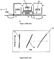
- FIG 1 there is shown a cross-sectional view of a non-volatile memory cell 10 of the prior art.
- the memory cell 10 comprises a single crystalline substrate 12, of a first conductivity type, such as P type.
- a first region 14 of a second conductivity type such as N type.
- a second region 16 Spaced apart from the first region 14 is a second region 16 also of the second conductivity type.
- a word line 20, made of polysilicon is positioned over a first portion of the channel region 18.
- the word line 20 is spaced apart from the channel region 18 by an silicon (di)oxide layer 22.
- a floating gate 24 which is also made of polysilicon, and is positioned over another portion of the channel region 18.
- the floating gate 24 is separated from the channel region 18 by another insulating layer 30, typically also of silicon (di)oxide.
- a coupling gate 26, also made of polysilicon is positioned over the floating gate 24 and is insulated therefrom by another insulating layer 32.
- an erase gate 28 also made of polysilicon. The erase gate 28 is positioned over the second region 16 and is insulated therefrom.
- the erase gate 28 is also immediately adjacent to but spaced apart from the coupling gate 26 and to another side of the coupling gate 26.
- charges stored on the floating gate 24 (or the absence of charges on the floating gate 24) control the flow of current between the first region 14 and the second region 16. Where the floating gate 24 has charges thereon, the floating gate 24 is programmed. Where the floating gate 24 does not have charges thereon, the floating gate 24 is erased.
- the memory cell 10 operates as follows. During the programming operation, when charges are stored on the floating gate 24, a first positive voltage is applied to the word line 20 causing the portion of the channel region 18 under the word line 20 to be conductive. A second positive voltage is applied to the coupling gate 26. A third positive voltage is applied to the second region 16. Current is applied to the first region 14. The electrons are attracted to the positive voltage at the second region 16. As they near the floating gate 24, they experience a sudden increase in the electric field caused by the voltage applied to the coupling gate 26, causing the charges to be injected onto the floating gate 24. Thus, programming occurs through the mechanism of hot electron injection. During the erase operation when charges are removed from the floating gate 24, a high positive voltage is applied to the erase gate 28.
- a negative voltage or ground voltage can be applied to the coupling gate 26 and/or the word line 20.
- Charges are transferrer from the floating gate 24 to the erase gate 28 by tunneling through the insulating layer between the floating gate 24 and the erase gate 28.
- the floating gate 24 may be formed with a sharp tip facing the erase gate 28, thereby facilitating the Fowler-Nordheim tunneling of electrons from the tip on the floating gate 24 and through the insulating layer between the floating gate 24 and the erase gate 28 onto the erase gate 28.
- a first positive voltage is applied to the word line 20 to turn on the portion of the channel region 18 beneath the word line 20.
- a second positive voltage is applied to the coupling gate 26.
- a voltage differential is applied to the first region 14 and the second region 16.
- the floating gate 24 were programmed, i.e. the floating gate 24 stores electrons, then the second positive voltage applied to the coupling gate 26 is not able to overcome the negative potential induced by electrons stored on the floating gate 24 and the portion of the channel region 18 beneath the floating gate 24 remains non-conductive. Thus, no current or a minimal amount of current would flow between the first region 14 and the second region 16. However, if the floating gate 24 were not programmed, i.e. the floating gate 24 is positively charged, then the second positive voltage applied to the coupling gate 26 is able to cause the portion of the channel region 18 beneath the floating gate 24 to be conductive. Thus, a current would flow between the first region 14 and the second region 16.
- memory cells 10 are typically formed in an array, having a plurality of rows and columns of memory cells 10, on a semiconductor wafer. After the devices are fabricated on a wafer, the devices on the wafer are subject to a test to determine the ability of each memory cell 10 to retain its programmed or erased state, in particular, the ability of the floating gate 24 in each memory cell 10 to retain its charge. During testing the memory cell 10 is first programmed, to place charges on the floating gate 24, or erased, to remove charges from the floating gate 24. The device is then subject to a high temperature bake. Finally, each memory cell 10 in the device is subject to a read operation in which the read current from the memory cell 10 under test is compared to the read reference current.
- FIG. 2 there is shown a graph of the read current of various memory cells with their data.
- the cells with the erased state typically would have a higher read current 40 compared to the read current 42 from memory cells with zero charge on the floating gates, which typically have a higher current than the read current 44 from the programmed memory cells. Due to dispersion of parameters of cell integrated in a memory array, the read current 42 of some cells can be higher than the read reference current, and the read current 42 of some cells can be lower than the read reference current.
- the read current from such a defective memory cell 10 having an erased state would decrease and tend to have the characteristics of current 42. This condition cannot be detected after a high temperature bake if the read current from the defective memory cell 10 under test remains above the read reference current. Similarly, the read current from a defective memory cell 10 having a programmed state, would increase and tend to have the characteristics of current 42. This condition cannot be detected after a high temperature bake if the read current from a defective memory cell 10 under test remains bellow the read reference current.
- testing of a memory device with memory cells 10 of the prior art have involved two steps.
- a first data pattern is stored in all memory devices followed by a first baking step, followed by a testing step to determine the read current of each memory cell 10 and compare them to the read reference current.
- a second data pattern which is a mutually inverse pattern of the first data pattern, is stored in all memory devices followed by a second baking step, followed by a testing step to determine the read current of each memory cell 10 and compare them to the read reference current. Because the time to store the data pattern in all memory devices and the time to bake the devices is considerable, this has increased the cost of testing the memory device.
- a defective cell 10 has a read current 42 above the read reference current.
- the read current from such a cell would decrease and tend to have the characteristics of current 42, so that its read current remains above the read reference current, and the defective cell 10 would not be detected.
- the second test when the defective cell 10 is in the programmed state, the read current from such a cell would increase and tend to have the characteristics of the read current 42.
- leakage is too slow during the bake process, the read current from the defective cell 10 would not have time to increase above the read reference current during the baking process.
- US-B-6772379 discloses an apparatus for verifying the data retention in non-volatile memories wherein an EEPROM leakage test is performed by use of thermal stress.
- one object of the present invention is to decrease the test time to determine data retention of a memory cell having a floating gate for the storage of charges thereon to determine if the memory cell has a leakage current from the floating gate.
- the memory cell which has a leak from the floating gate is characterized by the leakage current which is dependent upon the absolute value of the voltage of the floating gate.
- the method comprises the use of a first erase voltage and a first programming voltage, applied during normal operation, and a first read current detected during normal operation. In the method of the present invention, the method applies a voltage greater than the first erase voltage to over erase the floating gate.
- the memory cell including the floating gate is subject to a single high temperature bake. The memory cell is then tested for data retention of the floating gate based on the single high temperature bake.
- the method applies a voltage greater than the first programming voltage to over program the floating gate.
- the memory cell including the floating gate is subject to a single high temperature bake.
- the memory cell is then tested for data retention of the floating gate based on the single high temperature bake.
- the method of the present invention to improve the testing of data retention can be applied to all floating gate non-volatile memory cells and in particular those non-volatile memory cells 10 shown in Figure 1 .
- the method of the present invention has particular application to a floating gate non-volatile memory cell that has a leakage that is dependent upon the absolute value of the voltage programmed or erased on the floating gate.
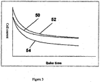
- FIG. 3 there is shown a graph 50 of a floating gate memory cell 10 which was erased with "normal” erase voltage, with its read current as a function of time.
- "normal” erase voltage it is meant the voltage that is used when the memory cell 10 is erased in operation.
- the graph 50 shows that as the memory cell 10 is baked over time, the read current decreases, asymptotically, and tends to have a value which corresponds to zero charge on the floating gate 24.
- the initial read current is large.
- the floating gate 24 loses positive charge, so the read current decreases overtime. It has been discovered that the leakage rate depends on the voltage on the floating gate 24.
- the graph 52 of the read current as a function of time would result.
- the speed of the decrease in the read current depends on the voltage on the floating gate 24, by over-erasing the memory cell 10 and baking the memory cell 10, the read current of a defective cell 10 would decrease faster than in the case of "normal" erase.
- a lower voltage or even zero or negative voltage is applied to the coupling gate 26 to sense the read current. The use of lower read voltage would result in lower read current and the graph 54 of the read current as a function of time would result.
- ⁇ Veg ( ⁇ Vcge- ⁇ Vcgr)*CRcg/(1-CReg); where ⁇ Veg is the difference between voltage that is applied to the erase gate 28 in the method of present invention during the erase operation and "normal" erase voltage, ⁇ Vcge is the difference between voltage which is applied to the coupling gate 26 in the method of present invention during the erase operation and voltage which is applied to the coupling gate 26 in the method of the prior art during the erase operation, ⁇ Vcgr is the difference between voltage which is applied to the coupling gate 26 in the method of present invention during the read operation and "normal" read voltage, C
- ⁇ Veg - ⁇ Vcgr*CRcg/(1-CReg).
- a memory cell 10 to be tested for data retention is first programmed with coupling gate programming voltage which is greater than the "normal” coupling gate programming voltage. After the memory cell 10 is over-programmed, a higher voltage than "normal” may be applied to the coupling gate 26 to sense the read current.
- the increase in the read current is faster when the voltage on the floating gate 24 is more negative Because of this phenomenon, by over-programming the memory cell 10 and baking the memory cell 10, the read current of memory cell that has a leakage from floating gate 24 may increase substantially such that it would be above the read reference current, and the memory cell 10 that has a leakage from floating gate is then detectable. In this manner it improves the detectability of a defective memory cell 10. It has been found that for optimal performance, the increase in programming voltage should be equal to the increase in read voltage.
- the memory cell 10 is subject to a single high temperature bake, and is then tested for the data retention of the memory cell 10 based upon the single high temperature bake. If the read current from the tested memory cell 10 is higher than the read reference current, then the memory cell 10 is deemed to be defective. Thus, with the method of the present invention, only a single high temperature bake process need to be applied and the data retention of the memory cell 10 may be tested.
- the over-erase or over-program voltage can be externally supplied to the test die containing the memory cells 10 of interest However, this may necessitate an extra pin to the die in the event the over-erase voltage or the over-program voltage is supplied on a dedicated pin. Alternatively, if the over-erase voltage or the over-program voltage is supplied on a pin to which other power/signal sources are also multiplexed, then this may necessitate additional circuitry within the die to distinguish between the over-erase voltage or the over-program voltage from the other power/signal.
- Another way to implement the method of the present invention is to generate the over-erase voltage or the over-program voltage internally on the die.
- Virtually all floating gate non-volatile memory cells have an on-board charge pump to generate the high voltage required for "normal" erase or programming functions.
- the on-board charge pump may be changed to generate an over-erase voltage or an over-program voltage.
- testing for data retention may be accomplished much faster than with the method of the prior art.
- the present invention reduces the testing time and improves screening efficiency.
- the absolute value of the potential on the floating gate during the baking process is higher, resulting in an acceleration of leakage, which results in a more efficient data retention screening.
Landscapes
- For Increasing The Reliability Of Semiconductor Memories (AREA)
- Read Only Memory (AREA)
- Semiconductor Memories (AREA)
- Non-Volatile Memory (AREA)
- Tests Of Electronic Circuits (AREA)
Claims (6)
- Procédé de mise à l'essai d'une conservation de données d'une cellule de mémoire non volatile (10) ayant une grille flottante (24) pour le stockage de charges sur celle-ci, ledit procédé mettant à l'essai la cellule de mémoire en cas de fuite de courant de la cellule de mémoire à partir de la grille flottante qui dépend de la valeur absolue de la tension de la grille flottante, dans lequel ladite cellule est actionnée par une première tension d'effacement, une première tension de programmation et une première tension de lecture, appliquées lors d'un fonctionnement normal, et un premier courant de lecture d'une cellule de mémoire effacée, détecté lors d'un fonctionnement normal, dans lequel ledit procédé est caractérisé par :l'application d'une tension supérieure à la première tension d'effacement pour sureffacer la grille flottante ;la soumission de la cellule de mémoire comprenant la grille flottante à une cuisson à haute température unique ; et par la suitela mise à l'essai de la conservation de données de la grille flottante en appliquant une tension de lecture inférieure à la première tension de lecture.
- Procédé selon la revendication 1, dans lequel ladite cellule de mémoire est caractérisée par :un substrat cristallin unique d'un premier type de conductivité et ayant une surface supérieure ;une première région d'un deuxième type de conductivité dans ledit substrat le long de la surface supérieure ;une deuxième région du deuxième type de conductivité, dans ledit substrat le long de la surface supérieure, espacée de la première région ;une région de canal entre la première région et la deuxième région ;une grille de ligne de mots positionnée sur une première partie de la région de canal, espacée de la région de canal par une première couche d'isolation ;une grille flottante positionnée sur une autre partie de la région de canal, adjacente à la grille de ligne de mots et séparée de celle-ci, dans lequel la grille flottante est séparée de la région de canal par une deuxième couche d'isolation ;une grille de couplage positionnée sur la grille flottante et isolée de celle-ci par une troisième couche d'isolation ; etune grille d'effacement, positionnée adjacente à la grille flottante et d'un côté opposé à la grille de ligne de mots ; ladite grille d'effacement étant positionnée sur la deuxième région et isolée de celle-ci.
- Procédé selon la revendication 2, dans lequel ladite étape de mise à l'essai détermine que la cellule de mémoire est défectueuse dans le cas où le courant de lecture de la cellule de mémoire après ladite étape de soumission est inférieur à un courant de référence de lecture.
- Procédé de mise à l'essai d'une conservation de données d'une cellule de mémoire non volatile (10) ayant une grille flottante (24) pour le stockage de charges sur celle-ci, ledit procédé mettant à l'essai la cellule de mémoire en cas de fuite de courant de la cellule de mémoire à partir de la grille flottante qui dépend de la valeur absolue de la tension de la grille flottante, dans lequel ladite cellule est actionnée par une première tension d'effacement, une première tension de programmation et une première tension de lecture, appliquées lors d'un fonctionnement normal, et un premier courant de lecture d'une cellule de mémoire programmée, détecté lors d'un fonctionnement normal, dans lequel ledit procédé est caractérisé par :l'application d'une tension supérieure à la première tension de programmation pour surprogrammer la grille flottante ;la soumission de la cellule de mémoire comprenant la grille flottante à une cuisson à haute température unique ; et par la suitela mise à l'essai de la conservation de données de la grille flottante en appliquant une tension de lecture supérieure à la première tension de lecture.
- Procédé selon la revendication 4, dans lequel ladite cellule de mémoire est caractérisée par :un substrat cristallin unique d'un premier type de conductivité et ayant une surface supérieure ;une première région d'un deuxième type de conductivité dans ledit substrat le long de la surface supérieure ;une deuxième région du deuxième type de conductivité, dans ledit substrat le long de la surface supérieure, espacée de la première région ;une région de canal entre la première région et la deuxième région ;une grille de ligne de mots positionnée sur une première partie de la région de canal, espacée de la région de canal par une première couche d'isolation ;une grille flottante positionnée sur une autre partie de la région de canal, adjacente à la grille de ligne de mots et séparée de celle-ci, dans lequel la grille flottante est séparée de la région de canal par une deuxième couche d'isolation ;une grille de couplage positionnée sur la grille flottante et isolée de celle-ci par une troisième couche d'isolation ; etune grille d'effacement, positionnée adjacente à la grille flottante et d'un côté opposé à la grille de ligne de mots ; ladite grille d'effacement étant positionnée sur la deuxième région et isolée de celle-ci.
- Procédé selon la revendication 5, dans lequel ladite étape de mise à l'essai détermine que la cellule de mémoire est défectueuse dans le cas où le courant de lecture de la cellule de mémoire après ladite étape de soumission est supérieur à un courant de référence de lecture.
Applications Claiming Priority (2)
| Application Number | Priority Date | Filing Date | Title |
|---|---|---|---|
| US13/293,056 US8576648B2 (en) | 2011-11-09 | 2011-11-09 | Method of testing data retention of a non-volatile memory cell having a floating gate |
| PCT/US2012/061386 WO2013070424A1 (fr) | 2011-11-09 | 2012-10-22 | Procédé d'essai de conservation de données d'une cellule de mémoire non volatile ayant une grille flottante |
Publications (3)
| Publication Number | Publication Date |
|---|---|
| EP2777065A1 EP2777065A1 (fr) | 2014-09-17 |
| EP2777065A4 EP2777065A4 (fr) | 2015-06-10 |
| EP2777065B1 true EP2777065B1 (fr) | 2016-12-07 |
Family
ID=48223563
Family Applications (1)
| Application Number | Title | Priority Date | Filing Date |
|---|---|---|---|
| EP12848380.7A Active EP2777065B1 (fr) | 2011-11-09 | 2012-10-22 | Procédé d'essai de conservation de données d'une cellule de mémoire non volatile ayant une grille flottante |
Country Status (7)
| Country | Link |
|---|---|
| US (1) | US8576648B2 (fr) |
| EP (1) | EP2777065B1 (fr) |
| JP (1) | JP5860545B2 (fr) |
| KR (1) | KR101458350B1 (fr) |
| CN (1) | CN103988281B (fr) |
| TW (1) | TWI515744B (fr) |
| WO (1) | WO2013070424A1 (fr) |
Cited By (1)
| Publication number | Priority date | Publication date | Assignee | Title |
|---|---|---|---|---|
| TWI721873B (zh) * | 2019-09-03 | 2021-03-11 | 美商超捷公司 | 在預定程式狀態中使用最終烘烤來改善類比非揮發性記憶體中之讀取電流穩定性的方法 |
Families Citing this family (14)
| Publication number | Priority date | Publication date | Assignee | Title |
|---|---|---|---|---|
| CN107768515B (zh) * | 2016-08-18 | 2020-05-08 | 华邦电子股份有限公司 | 存储器装置的形成方法 |
| US10714489B2 (en) | 2018-08-23 | 2020-07-14 | Silicon Storage Technology, Inc. | Method of programming a split-gate flash memory cell with erase gate |
| CN109545264B (zh) * | 2018-10-31 | 2020-10-16 | 大唐微电子技术有限公司 | 一种对含闪存flash芯片的晶圆级测试方法、装置 |
| US10878905B1 (en) * | 2019-07-02 | 2020-12-29 | Microchip Technology Inc. | Metal filament ReRAM cell with current limiting during program and erase |
| CN110942800B (zh) * | 2019-12-13 | 2021-04-09 | 长江存储科技有限责任公司 | 一种三维存储器数据保留能力测试结构及测试方法 |
| CN111145825B (zh) * | 2019-12-31 | 2021-09-24 | 长江存储科技有限责任公司 | 存储结构电荷保持性能的检测方法及检测装置 |
| US12020762B2 (en) * | 2021-09-27 | 2024-06-25 | Silicon Storage Technology, Inc. | Method of determining defective die containing non-volatile memory cells |
| KR20230052022A (ko) * | 2021-10-12 | 2023-04-19 | 삼성전자주식회사 | 메모리 제어 방법 및 상기 방법을 수행하는 전자 장치 |
| US12014793B2 (en) | 2022-04-13 | 2024-06-18 | Silicon Storage Technology, Inc. | Method of screening non-volatile memory cells |
| EP4508640B1 (fr) * | 2022-04-13 | 2026-02-25 | Silicon Storage Technology, Inc. | Procédé de filtrage de cellules de mémoire non volatile |
| CN115762614A (zh) * | 2022-11-24 | 2023-03-07 | 华虹半导体(无锡)有限公司 | 一种筛查晶圆缺陷的测试方法 |
| CN116500406A (zh) * | 2023-04-27 | 2023-07-28 | 上海华虹宏力半导体制造有限公司 | 一种晶圆测试参数的筛选方法 |
| KR102854883B1 (ko) * | 2024-12-23 | 2025-09-04 | 고려대학교 세종산학협력단 | 3차원 반도체 게이트 적층 구조에서 수직 측벽에 대한 전기적 특성을 평가하는 분석 방법 및 장치 |
| CN119851743B (zh) * | 2025-01-02 | 2025-11-28 | 上海华虹宏力半导体制造有限公司 | 闪存测试方法 |
Family Cites Families (17)
| Publication number | Priority date | Publication date | Assignee | Title |
|---|---|---|---|---|
| JPS5610942A (en) * | 1979-07-05 | 1981-02-03 | Nec Corp | Inspection of memory retaining capacity of semiconductor nonvolatile memory |
| US4809231A (en) * | 1987-11-12 | 1989-02-28 | Motorola, Inc. | Method and apparatus for post-packaging testing of one-time programmable memories |
| JPH052896A (ja) * | 1991-06-25 | 1993-01-08 | Fujitsu Ltd | 不揮発性半導体記憶装置およびその試験方法 |
| JP3236105B2 (ja) * | 1993-03-17 | 2001-12-10 | 富士通株式会社 | 不揮発性半導体記憶装置及びその動作試験方法 |
| JPH07153300A (ja) * | 1993-11-29 | 1995-06-16 | Hitachi Ltd | 不揮発性メモリおよびそのスクリーニング方法 |
| JPH0927198A (ja) * | 1995-07-10 | 1997-01-28 | Mitsubishi Electric Corp | 不揮発性半導体記憶装置の信頼性評価方法およびその不揮発性半導体記憶装置 |
| IT1313865B1 (it) * | 1999-11-11 | 2002-09-24 | St Microelectronics Srl | Apparato per la verifica della ritenzione di dati in memorie nonvolatili. |
| JP2002100192A (ja) | 2000-09-22 | 2002-04-05 | Toshiba Corp | 不揮発性半導体メモリ |
| US20040049724A1 (en) | 2002-07-22 | 2004-03-11 | Colin Bill | Built-in-self-test (BIST) of flash memory cells and implementation of BIST interface |
| JP3721159B2 (ja) * | 2002-11-28 | 2005-11-30 | 株式会社東芝 | 不揮発性半導体記憶装置 |
| US20050035429A1 (en) | 2003-08-15 | 2005-02-17 | Yeh Chih Chieh | Programmable eraseless memory |
| US7145186B2 (en) | 2004-08-24 | 2006-12-05 | Micron Technology, Inc. | Memory cell with trenched gated thyristor |
| JP2007149187A (ja) * | 2005-11-25 | 2007-06-14 | Renesas Technology Corp | 半導体装置 |
| US7948799B2 (en) | 2006-05-23 | 2011-05-24 | Macronix International Co., Ltd. | Structure and method of sub-gate NAND memory with bandgap engineered SONOS devices |
| US7839695B2 (en) | 2007-04-27 | 2010-11-23 | Macronix International Co., Ltd. | High temperature methods for enhancing retention characteristics of memory devices |
| US7864588B2 (en) | 2007-09-17 | 2011-01-04 | Spansion Israel Ltd. | Minimizing read disturb in an array flash cell |
| JP2010176750A (ja) * | 2009-01-29 | 2010-08-12 | Oki Semiconductor Co Ltd | 不揮発性半導体メモリ及びそのリーク不良検出方法 |
-
2011
- 2011-11-09 US US13/293,056 patent/US8576648B2/en active Active
-
2012
- 2012-10-22 EP EP12848380.7A patent/EP2777065B1/fr active Active
- 2012-10-22 CN CN201280055415.8A patent/CN103988281B/zh active Active
- 2012-10-22 WO PCT/US2012/061386 patent/WO2013070424A1/fr not_active Ceased
- 2012-10-22 KR KR1020147014676A patent/KR101458350B1/ko active Active
- 2012-10-22 JP JP2014541085A patent/JP5860545B2/ja active Active
- 2012-11-01 TW TW101140508A patent/TWI515744B/zh active
Cited By (1)
| Publication number | Priority date | Publication date | Assignee | Title |
|---|---|---|---|---|
| TWI721873B (zh) * | 2019-09-03 | 2021-03-11 | 美商超捷公司 | 在預定程式狀態中使用最終烘烤來改善類比非揮發性記憶體中之讀取電流穩定性的方法 |
Also Published As
| Publication number | Publication date |
|---|---|
| EP2777065A4 (fr) | 2015-06-10 |
| JP2015502000A (ja) | 2015-01-19 |
| JP5860545B2 (ja) | 2016-02-16 |
| US20130114337A1 (en) | 2013-05-09 |
| EP2777065A1 (fr) | 2014-09-17 |
| US8576648B2 (en) | 2013-11-05 |
| KR20140076640A (ko) | 2014-06-20 |
| WO2013070424A1 (fr) | 2013-05-16 |
| TWI515744B (zh) | 2016-01-01 |
| CN103988281A (zh) | 2014-08-13 |
| TW201333966A (zh) | 2013-08-16 |
| CN103988281B (zh) | 2016-06-22 |
| KR101458350B1 (ko) | 2014-11-12 |
Similar Documents
| Publication | Publication Date | Title |
|---|---|---|
| EP2777065B1 (fr) | Procédé d'essai de conservation de données d'une cellule de mémoire non volatile ayant une grille flottante | |
| WO1996011475A1 (fr) | Procede d'elimination du piegeage d'electrons induit par cyclage, dans l'oxyde a effet tunnel des memoires flash eeprom de seulement 5 volts | |
| US20070268749A1 (en) | Method for operating non-volatile memory device | |
| US7319615B1 (en) | Ramp gate erase for dual bit flash memory | |
| US5481494A (en) | Method for tightening VT distribution of 5 volt-only flash EEPROMS | |
| US8953378B2 (en) | Split gate programming | |
| US12014793B2 (en) | Method of screening non-volatile memory cells | |
| US7203095B2 (en) | Method for determining programming voltage of nonvolatile memory | |
| US20130194875A1 (en) | Structure and method for healing tunnel dielectric of non-volatile memory cells | |
| US9136009B1 (en) | Method to improve accuracy of a low voltage state in flash memory cells | |
| EP4348651B1 (fr) | Procédé d'amélioration de la stabilité de courant de lecture dans une mémoire non volatile analogique par réglage post-programme pour des cellules de mémoire présentant un bruit de télégraphe aléatoire | |
| KR102748492B1 (ko) | 비휘발성 메모리 셀들을 스크리닝하는 방법 | |
| US6800493B2 (en) | Pre-erase manufacturing method | |
| US7170796B1 (en) | Methods and systems for reducing the threshold voltage distribution following a memory cell erase | |
| KR20100056747A (ko) | 플래시 메모리 소자의 프로그램 방법 | |
| TW201638954A (zh) | 用於程式化分離閘非揮發性記憶體單元之系統及方法 | |
| US9449713B2 (en) | Method for preconditioning thin film storage array for data retention | |
| US20080049512A1 (en) | Nonvolatile memory device and method of programming the same | |
| CN112652352B (zh) | 闪存的数据保持力测试方法 | |
| US6781885B1 (en) | Method of programming a memory cell | |
| KR100557220B1 (ko) | 비 휘발성 메모리 셀을 구비한 반도체 장치의구동방법 |
Legal Events
| Date | Code | Title | Description |
|---|---|---|---|
| PUAI | Public reference made under article 153(3) epc to a published international application that has entered the european phase |
Free format text: ORIGINAL CODE: 0009012 |
|
| 17P | Request for examination filed |
Effective date: 20140610 |
|
| AK | Designated contracting states |
Kind code of ref document: A1 Designated state(s): AL AT BE BG CH CY CZ DE DK EE ES FI FR GB GR HR HU IE IS IT LI LT LU LV MC MK MT NL NO PL PT RO RS SE SI SK SM TR |
|
| DAX | Request for extension of the european patent (deleted) | ||
| REG | Reference to a national code |
Ref country code: DE Ref legal event code: R079 Ref document number: 602012026452 Country of ref document: DE Free format text: PREVIOUS MAIN CLASS: H01L0021020000 Ipc: G11C0029500000 |
|
| RA4 | Supplementary search report drawn up and despatched (corrected) |
Effective date: 20150513 |
|
| RIC1 | Information provided on ipc code assigned before grant |
Ipc: G11C 29/50 20060101AFI20150507BHEP Ipc: G11C 29/06 20060101ALI20150507BHEP |
|
| RIN1 | Information on inventor provided before grant (corrected) |
Inventor name: MARKOV, VIKTOR Inventor name: BANSAL, SATISH Inventor name: KOTOV, ALEXANDER Inventor name: YOO, JONG-WON |
|
| GRAP | Despatch of communication of intention to grant a patent |
Free format text: ORIGINAL CODE: EPIDOSNIGR1 |
|
| INTG | Intention to grant announced |
Effective date: 20160212 |
|
| RAP1 | Party data changed (applicant data changed or rights of an application transferred) |
Owner name: SILICON STORAGE TECHNOLOGY, INC. |
|
| GRAP | Despatch of communication of intention to grant a patent |
Free format text: ORIGINAL CODE: EPIDOSNIGR1 |
|
| INTG | Intention to grant announced |
Effective date: 20160603 |
|
| GRAS | Grant fee paid |
Free format text: ORIGINAL CODE: EPIDOSNIGR3 |
|
| GRAA | (expected) grant |
Free format text: ORIGINAL CODE: 0009210 |
|
| AK | Designated contracting states |
Kind code of ref document: B1 Designated state(s): AL AT BE BG CH CY CZ DE DK EE ES FI FR GB GR HR HU IE IS IT LI LT LU LV MC MK MT NL NO PL PT RO RS SE SI SK SM TR |
|
| REG | Reference to a national code |
Ref country code: GB Ref legal event code: FG4D |
|
| REG | Reference to a national code |
Ref country code: CH Ref legal event code: EP Ref country code: AT Ref legal event code: REF Ref document number: 852365 Country of ref document: AT Kind code of ref document: T Effective date: 20161215 |
|
| REG | Reference to a national code |
Ref country code: IE Ref legal event code: FG4D |
|
| REG | Reference to a national code |
Ref country code: DE Ref legal event code: R096 Ref document number: 602012026452 Country of ref document: DE |
|
| REG | Reference to a national code |
Ref country code: NL Ref legal event code: FP |
|
| PG25 | Lapsed in a contracting state [announced via postgrant information from national office to epo] |
Ref country code: LV Free format text: LAPSE BECAUSE OF FAILURE TO SUBMIT A TRANSLATION OF THE DESCRIPTION OR TO PAY THE FEE WITHIN THE PRESCRIBED TIME-LIMIT Effective date: 20161207 |
|
| REG | Reference to a national code |
Ref country code: LT Ref legal event code: MG4D |
|
| PG25 | Lapsed in a contracting state [announced via postgrant information from national office to epo] |
Ref country code: NO Free format text: LAPSE BECAUSE OF FAILURE TO SUBMIT A TRANSLATION OF THE DESCRIPTION OR TO PAY THE FEE WITHIN THE PRESCRIBED TIME-LIMIT Effective date: 20170307 Ref country code: LT Free format text: LAPSE BECAUSE OF FAILURE TO SUBMIT A TRANSLATION OF THE DESCRIPTION OR TO PAY THE FEE WITHIN THE PRESCRIBED TIME-LIMIT Effective date: 20161207 Ref country code: GR Free format text: LAPSE BECAUSE OF FAILURE TO SUBMIT A TRANSLATION OF THE DESCRIPTION OR TO PAY THE FEE WITHIN THE PRESCRIBED TIME-LIMIT Effective date: 20170308 Ref country code: SE Free format text: LAPSE BECAUSE OF FAILURE TO SUBMIT A TRANSLATION OF THE DESCRIPTION OR TO PAY THE FEE WITHIN THE PRESCRIBED TIME-LIMIT Effective date: 20161207 |
|
| PG25 | Lapsed in a contracting state [announced via postgrant information from national office to epo] |
Ref country code: HR Free format text: LAPSE BECAUSE OF FAILURE TO SUBMIT A TRANSLATION OF THE DESCRIPTION OR TO PAY THE FEE WITHIN THE PRESCRIBED TIME-LIMIT Effective date: 20161207 Ref country code: ES Free format text: LAPSE BECAUSE OF FAILURE TO SUBMIT A TRANSLATION OF THE DESCRIPTION OR TO PAY THE FEE WITHIN THE PRESCRIBED TIME-LIMIT Effective date: 20161207 Ref country code: RS Free format text: LAPSE BECAUSE OF FAILURE TO SUBMIT A TRANSLATION OF THE DESCRIPTION OR TO PAY THE FEE WITHIN THE PRESCRIBED TIME-LIMIT Effective date: 20161207 Ref country code: FI Free format text: LAPSE BECAUSE OF FAILURE TO SUBMIT A TRANSLATION OF THE DESCRIPTION OR TO PAY THE FEE WITHIN THE PRESCRIBED TIME-LIMIT Effective date: 20161207 |
|
| PG25 | Lapsed in a contracting state [announced via postgrant information from national office to epo] |
Ref country code: IS Free format text: LAPSE BECAUSE OF FAILURE TO SUBMIT A TRANSLATION OF THE DESCRIPTION OR TO PAY THE FEE WITHIN THE PRESCRIBED TIME-LIMIT Effective date: 20170407 Ref country code: RO Free format text: LAPSE BECAUSE OF FAILURE TO SUBMIT A TRANSLATION OF THE DESCRIPTION OR TO PAY THE FEE WITHIN THE PRESCRIBED TIME-LIMIT Effective date: 20161207 Ref country code: CZ Free format text: LAPSE BECAUSE OF FAILURE TO SUBMIT A TRANSLATION OF THE DESCRIPTION OR TO PAY THE FEE WITHIN THE PRESCRIBED TIME-LIMIT Effective date: 20161207 Ref country code: EE Free format text: LAPSE BECAUSE OF FAILURE TO SUBMIT A TRANSLATION OF THE DESCRIPTION OR TO PAY THE FEE WITHIN THE PRESCRIBED TIME-LIMIT Effective date: 20161207 Ref country code: SK Free format text: LAPSE BECAUSE OF FAILURE TO SUBMIT A TRANSLATION OF THE DESCRIPTION OR TO PAY THE FEE WITHIN THE PRESCRIBED TIME-LIMIT Effective date: 20161207 |
|
| PG25 | Lapsed in a contracting state [announced via postgrant information from national office to epo] |
Ref country code: BG Free format text: LAPSE BECAUSE OF FAILURE TO SUBMIT A TRANSLATION OF THE DESCRIPTION OR TO PAY THE FEE WITHIN THE PRESCRIBED TIME-LIMIT Effective date: 20170307 Ref country code: BE Free format text: LAPSE BECAUSE OF FAILURE TO SUBMIT A TRANSLATION OF THE DESCRIPTION OR TO PAY THE FEE WITHIN THE PRESCRIBED TIME-LIMIT Effective date: 20161207 Ref country code: PT Free format text: LAPSE BECAUSE OF FAILURE TO SUBMIT A TRANSLATION OF THE DESCRIPTION OR TO PAY THE FEE WITHIN THE PRESCRIBED TIME-LIMIT Effective date: 20170407 Ref country code: PL Free format text: LAPSE BECAUSE OF FAILURE TO SUBMIT A TRANSLATION OF THE DESCRIPTION OR TO PAY THE FEE WITHIN THE PRESCRIBED TIME-LIMIT Effective date: 20161207 Ref country code: SM Free format text: LAPSE BECAUSE OF FAILURE TO SUBMIT A TRANSLATION OF THE DESCRIPTION OR TO PAY THE FEE WITHIN THE PRESCRIBED TIME-LIMIT Effective date: 20161207 |
|
| REG | Reference to a national code |
Ref country code: DE Ref legal event code: R097 Ref document number: 602012026452 Country of ref document: DE |
|
| REG | Reference to a national code |
Ref country code: FR Ref legal event code: PLFP Year of fee payment: 6 |
|
| PLBE | No opposition filed within time limit |
Free format text: ORIGINAL CODE: 0009261 |
|
| STAA | Information on the status of an ep patent application or granted ep patent |
Free format text: STATUS: NO OPPOSITION FILED WITHIN TIME LIMIT |
|
| 26N | No opposition filed |
Effective date: 20170908 |
|
| PG25 | Lapsed in a contracting state [announced via postgrant information from national office to epo] |
Ref country code: SI Free format text: LAPSE BECAUSE OF FAILURE TO SUBMIT A TRANSLATION OF THE DESCRIPTION OR TO PAY THE FEE WITHIN THE PRESCRIBED TIME-LIMIT Effective date: 20161207 Ref country code: DK Free format text: LAPSE BECAUSE OF FAILURE TO SUBMIT A TRANSLATION OF THE DESCRIPTION OR TO PAY THE FEE WITHIN THE PRESCRIBED TIME-LIMIT Effective date: 20161207 |
|
| PG25 | Lapsed in a contracting state [announced via postgrant information from national office to epo] |
Ref country code: MC Free format text: LAPSE BECAUSE OF FAILURE TO SUBMIT A TRANSLATION OF THE DESCRIPTION OR TO PAY THE FEE WITHIN THE PRESCRIBED TIME-LIMIT Effective date: 20161207 |
|
| REG | Reference to a national code |
Ref country code: CH Ref legal event code: PL |
|
| REG | Reference to a national code |
Ref country code: IE Ref legal event code: MM4A |
|
| PG25 | Lapsed in a contracting state [announced via postgrant information from national office to epo] |
Ref country code: LI Free format text: LAPSE BECAUSE OF NON-PAYMENT OF DUE FEES Effective date: 20171031 Ref country code: LU Free format text: LAPSE BECAUSE OF NON-PAYMENT OF DUE FEES Effective date: 20171022 Ref country code: CH Free format text: LAPSE BECAUSE OF NON-PAYMENT OF DUE FEES Effective date: 20171031 |
|
| REG | Reference to a national code |
Ref country code: FR Ref legal event code: PLFP Year of fee payment: 7 |
|
| PG25 | Lapsed in a contracting state [announced via postgrant information from national office to epo] |
Ref country code: MT Free format text: LAPSE BECAUSE OF NON-PAYMENT OF DUE FEES Effective date: 20171022 |
|
| PG25 | Lapsed in a contracting state [announced via postgrant information from national office to epo] |
Ref country code: IE Free format text: LAPSE BECAUSE OF NON-PAYMENT OF DUE FEES Effective date: 20171022 |
|
| REG | Reference to a national code |
Ref country code: AT Ref legal event code: UEP Ref document number: 852365 Country of ref document: AT Kind code of ref document: T Effective date: 20161207 |
|
| PG25 | Lapsed in a contracting state [announced via postgrant information from national office to epo] |
Ref country code: HU Free format text: LAPSE BECAUSE OF FAILURE TO SUBMIT A TRANSLATION OF THE DESCRIPTION OR TO PAY THE FEE WITHIN THE PRESCRIBED TIME-LIMIT; INVALID AB INITIO Effective date: 20121022 |
|
| PG25 | Lapsed in a contracting state [announced via postgrant information from national office to epo] |
Ref country code: CY Free format text: LAPSE BECAUSE OF NON-PAYMENT OF DUE FEES Effective date: 20161207 |
|
| PG25 | Lapsed in a contracting state [announced via postgrant information from national office to epo] |
Ref country code: MK Free format text: LAPSE BECAUSE OF FAILURE TO SUBMIT A TRANSLATION OF THE DESCRIPTION OR TO PAY THE FEE WITHIN THE PRESCRIBED TIME-LIMIT Effective date: 20161207 |
|
| PG25 | Lapsed in a contracting state [announced via postgrant information from national office to epo] |
Ref country code: TR Free format text: LAPSE BECAUSE OF FAILURE TO SUBMIT A TRANSLATION OF THE DESCRIPTION OR TO PAY THE FEE WITHIN THE PRESCRIBED TIME-LIMIT Effective date: 20161207 |
|
| PG25 | Lapsed in a contracting state [announced via postgrant information from national office to epo] |
Ref country code: AL Free format text: LAPSE BECAUSE OF FAILURE TO SUBMIT A TRANSLATION OF THE DESCRIPTION OR TO PAY THE FEE WITHIN THE PRESCRIBED TIME-LIMIT Effective date: 20161207 |
|
| P01 | Opt-out of the competence of the unified patent court (upc) registered |
Effective date: 20230528 |
|
| PGFP | Annual fee paid to national office [announced via postgrant information from national office to epo] |
Ref country code: NL Payment date: 20250923 Year of fee payment: 14 Ref country code: IT Payment date: 20250923 Year of fee payment: 14 |
|
| PGFP | Annual fee paid to national office [announced via postgrant information from national office to epo] |
Ref country code: GB Payment date: 20250923 Year of fee payment: 14 |
|
| PGFP | Annual fee paid to national office [announced via postgrant information from national office to epo] |
Ref country code: FR Payment date: 20250924 Year of fee payment: 14 |
|
| PGFP | Annual fee paid to national office [announced via postgrant information from national office to epo] |
Ref country code: DE Payment date: 20250923 Year of fee payment: 14 |
|
| PGFP | Annual fee paid to national office [announced via postgrant information from national office to epo] |
Ref country code: AT Payment date: 20250926 Year of fee payment: 14 |