EP2769264B1 - Schreibvorgänge auf einem elektronischen abbildungssubstrat - Google Patents
Schreibvorgänge auf einem elektronischen abbildungssubstrat Download PDFInfo
- Publication number
- EP2769264B1 EP2769264B1 EP11874298.0A EP11874298A EP2769264B1 EP 2769264 B1 EP2769264 B1 EP 2769264B1 EP 11874298 A EP11874298 A EP 11874298A EP 2769264 B1 EP2769264 B1 EP 2769264B1
- Authority
- EP
- European Patent Office
- Prior art keywords
- electronic imaging
- writing device
- imaging substrate
- writing
- substrate
- Prior art date
- Legal status (The legal status is an assumption and is not a legal conclusion. Google has not performed a legal analysis and makes no representation as to the accuracy of the status listed.)
- Active
Links
Images


Classifications
-
- B—PERFORMING OPERATIONS; TRANSPORTING
- B41—PRINTING; LINING MACHINES; TYPEWRITERS; STAMPS
- B41J—TYPEWRITERS; SELECTIVE PRINTING MECHANISMS, i.e. MECHANISMS PRINTING OTHERWISE THAN FROM A FORME; CORRECTION OF TYPOGRAPHICAL ERRORS
- B41J3/00—Typewriters or selective printing or marking mechanisms characterised by the purpose for which they are constructed
- B41J3/407—Typewriters or selective printing or marking mechanisms characterised by the purpose for which they are constructed for marking on special material
- B41J3/4076—Typewriters or selective printing or marking mechanisms characterised by the purpose for which they are constructed for marking on special material printing on rewritable, bistable "electronic paper" by a focused electric or magnetic field
-
- G—PHYSICS
- G02—OPTICS
- G02F—OPTICAL DEVICES OR ARRANGEMENTS FOR THE CONTROL OF LIGHT BY MODIFICATION OF THE OPTICAL PROPERTIES OF THE MEDIA OF THE ELEMENTS INVOLVED THEREIN; NON-LINEAR OPTICS; FREQUENCY-CHANGING OF LIGHT; OPTICAL LOGIC ELEMENTS; OPTICAL ANALOGUE/DIGITAL CONVERTERS
- G02F1/00—Devices or arrangements for the control of the intensity, colour, phase, polarisation or direction of light arriving from an independent light source, e.g. switching, gating or modulating; Non-linear optics
- G02F1/01—Devices or arrangements for the control of the intensity, colour, phase, polarisation or direction of light arriving from an independent light source, e.g. switching, gating or modulating; Non-linear optics for the control of the intensity, phase, polarisation or colour
- G02F1/165—Devices or arrangements for the control of the intensity, colour, phase, polarisation or direction of light arriving from an independent light source, e.g. switching, gating or modulating; Non-linear optics for the control of the intensity, phase, polarisation or colour based on translational movement of particles in a fluid under the influence of an applied field
- G02F1/166—Devices or arrangements for the control of the intensity, colour, phase, polarisation or direction of light arriving from an independent light source, e.g. switching, gating or modulating; Non-linear optics for the control of the intensity, phase, polarisation or colour based on translational movement of particles in a fluid under the influence of an applied field characterised by the electro-optical or magneto-optical effect
- G02F1/167—Devices or arrangements for the control of the intensity, colour, phase, polarisation or direction of light arriving from an independent light source, e.g. switching, gating or modulating; Non-linear optics for the control of the intensity, phase, polarisation or colour based on translational movement of particles in a fluid under the influence of an applied field characterised by the electro-optical or magneto-optical effect by electrophoresis
-
- G—PHYSICS
- G09—EDUCATION; CRYPTOGRAPHY; DISPLAY; ADVERTISING; SEALS
- G09G—ARRANGEMENTS OR CIRCUITS FOR CONTROL OF INDICATING DEVICES USING STATIC MEANS TO PRESENT VARIABLE INFORMATION
- G09G3/00—Control arrangements or circuits, of interest only in connection with visual indicators other than cathode-ray tubes
- G09G3/20—Control arrangements or circuits, of interest only in connection with visual indicators other than cathode-ray tubes for presentation of an assembly of a number of characters, e.g. a page, by composing the assembly by combination of individual elements arranged in a matrix no fixed position being assigned to or needed to be assigned to the individual characters or partial characters
- G09G3/34—Control arrangements or circuits, of interest only in connection with visual indicators other than cathode-ray tubes for presentation of an assembly of a number of characters, e.g. a page, by composing the assembly by combination of individual elements arranged in a matrix no fixed position being assigned to or needed to be assigned to the individual characters or partial characters by control of light from an independent source
- G09G3/3433—Control arrangements or circuits, of interest only in connection with visual indicators other than cathode-ray tubes for presentation of an assembly of a number of characters, e.g. a page, by composing the assembly by combination of individual elements arranged in a matrix no fixed position being assigned to or needed to be assigned to the individual characters or partial characters by control of light from an independent source using light modulating elements actuated by an electric field and being other than liquid crystal devices and electrochromic devices
- G09G3/344—Control arrangements or circuits, of interest only in connection with visual indicators other than cathode-ray tubes for presentation of an assembly of a number of characters, e.g. a page, by composing the assembly by combination of individual elements arranged in a matrix no fixed position being assigned to or needed to be assigned to the individual characters or partial characters by control of light from an independent source using light modulating elements actuated by an electric field and being other than liquid crystal devices and electrochromic devices based on particles moving in a fluid or in a gas, e.g. electrophoretic devices
-
- G—PHYSICS
- G02—OPTICS
- G02F—OPTICAL DEVICES OR ARRANGEMENTS FOR THE CONTROL OF LIGHT BY MODIFICATION OF THE OPTICAL PROPERTIES OF THE MEDIA OF THE ELEMENTS INVOLVED THEREIN; NON-LINEAR OPTICS; FREQUENCY-CHANGING OF LIGHT; OPTICAL LOGIC ELEMENTS; OPTICAL ANALOGUE/DIGITAL CONVERTERS
- G02F1/00—Devices or arrangements for the control of the intensity, colour, phase, polarisation or direction of light arriving from an independent light source, e.g. switching, gating or modulating; Non-linear optics
- G02F1/01—Devices or arrangements for the control of the intensity, colour, phase, polarisation or direction of light arriving from an independent light source, e.g. switching, gating or modulating; Non-linear optics for the control of the intensity, phase, polarisation or colour
- G02F1/165—Devices or arrangements for the control of the intensity, colour, phase, polarisation or direction of light arriving from an independent light source, e.g. switching, gating or modulating; Non-linear optics for the control of the intensity, phase, polarisation or colour based on translational movement of particles in a fluid under the influence of an applied field
- G02F1/1675—Constructional details
- G02F1/16757—Microcapsules
-
- G—PHYSICS
- G09—EDUCATION; CRYPTOGRAPHY; DISPLAY; ADVERTISING; SEALS
- G09G—ARRANGEMENTS OR CIRCUITS FOR CONTROL OF INDICATING DEVICES USING STATIC MEANS TO PRESENT VARIABLE INFORMATION
- G09G2380/00—Specific applications
Definitions
- Electronic paper is a type of electronic display designed to reflect ambient light back to the viewer. This is opposed to traditional display technologies that emit rather than reflect light. Electronic paper is thus designed to mimic the appearance of ink on physical paper.
- One type of electronic paper display is an electrophoretic display.
- One type of electrophoretic display includes a two dimensional array of microcapsules. Each microcapsule includes a number of particles suspended in a liquid. In one example, the particles include both white particles and black particles. These two different colors of particles are oppositely charged. By manipulating an electric field across each microcapsule, that microcapsule can be switched to appear white or black.
- One way to manipulate the electric field is to form an array of switching circuitry underneath the array of microcapsules.
- This switching circuitry addresses each microcapsule individually to switch the state of that microcapsule to either display a white or black color to a human viewer.
- the costs of manufacturing such electronic paper displays are due primarily to the cost of the switching circuitry used to change the state of the display.
- US patent application US2006/017659 describes an electronic paper display system wherein a transfer apparatus wirelessly transfers information to a display apparatus comprising an electronic paper unit.
- US5,225,856 describes reducing blooming artefacts in an iconographic imaging device by summing the effects of previously deposited charge to determine the likely displacement of an ion due to the previously deposited charge. Ions are then deposited or not deposited based on this determination.
- one way to manipulate the electric field in order to cause an image to be displayed on the electronic paper is to form an array of switching circuitry underneath the array of microcapsules.
- This switching circuitry addresses each microcapsule individually to switch the state of that microcapsule to either display a white or black color to a human viewer.
- the costs of manufacturing such electronic paper displays are due primarily to the cost of the switching circuitry used to change the state of the display.
- an electronic imaging substrate as the electronic paper display.
- the electronic imaging substrate includes the microcapsule array without the circuitry underneath.
- An external writing device is then used to change the state of the electronic imaging substrate so that it displays the desired image.
- This external writing device may be, for example, an ion head.
- the ion head projects a beam of charged particles. When these charged particles reach the surface of a microcapsule, the oppositely charged particles within the microcapsule will be pulled toward the surface, thus changing the state of that microcapsule.
- an access card may include a region that is made of an electronic imaging substrate.
- the time and date stamp may be written onto the electronic imaging substrate region using an external writing device.
- Various other security features may be printed onto that region as well.
- a gift card may display the amount of money left on that card. When that gift card is used, the external writing device may rewrite the electronic imaging region of that card so that the new balance is displayed.
- One issue with using an external writing device to change the state of an electronic imaging substrate is an effect referred to as blooming.
- the electronic imaging substrate is moved in relation to the writing device.
- the writing device is modulated to produce the appropriate particle beam at certain regions on the electronic imaging substrate to form the desired image.
- a gap between the substrate and the writing device is maintained. This gap allows for the blooming effect to occur because the electric field created within the gap between the writing device and the imaging substrate is such that it pushes the particles that are projected from the writing device outward rather than straight.
- This blooming effect results in a larger set of microcapsules than desired being altered during the writing process. A particular dot or line may be larger than intended. The blooming effect thus reduces the precision with which an external writing device may rewrite the images on the electronic imaging substrate.
- the present specification discloses methods and systems for rewriting the state of an electronic imaging substrate with an external device while minimizing blooming effects.
- the writing device makes contact with or comes very close to the surface of the electronic imaging substrate during the writing process. By eliminating the gap between the writing head and the electronic imaging substrate, the blooming effect is sufficiently reduced.
- the writing device As the electronic imaging substrate passes in relation to the writing device while the writing device maintains a specified distance from the imaging substrate.
- the writing device comes to a region of the electronic imaging substrate where the state of the image is to be changed, then the movement between the writing device and substrate is stopped.
- the writing device is then lowered to make contact with the electronic imaging device to change the state of the image cells at that region.
- the writing device is then moved away from the imaging substrate so that the movement of the electronic imaging substrate in relation to the writing head can continue.
- the resolution at which the external writing device is able to print is greatly increased as a result of the reduced blooming effect.
- the increase in the amount of time it takes to rewrite the electronic imaging substrate is not problematic.
- the overall writing process may take only a few seconds rather than a few microseconds.
- Fig. 1A is a diagram showing an illustrative image cell (100).
- image cell 100
- FIG. 1A illustrates these principles as they apply to an electrophoretic display technology.
- each image cell corresponds to a microcapsule.
- the image cell (100) includes a number of black particles (102) and a number of white particles (104).
- the particles (102) are suspended within a liquid polymer (106) within the image cell (100).
- the black particles (102) are negatively charged while the white particles (104) are positively charged.
- an electric field applied across the image cell will move all of the negatively charged white particles (104) and all of the positively charged black particles to the other end.
- the polarity of the electric field can be reversed so that the image cell can take on either a white appearance or a black appearance.
- images can be formed within that array by selectively applying an electric field across certain image cells in order to form the desired image.
- Fig. 1B is a diagram showing an illustrative cross-sectional view of a portion of an electronic imaging substrate (110).
- the electronic imaging substrate includes an image cell layer (116).
- the image cell layer includes an array of image cells (100).
- a transparent conductor (112) is placed on one side of the image cell layer (116). This transparent conductor can then be grounded. As will be described in further detail below, the transparent conductor is used to hold charges in order to produce the desired electric fields used to change the state of the image cells.
- a transparent material (114) such as transparent mylar is then placed adjacent to the transparent conductor.
- This transparent material serves as the surface of the electronic imaging substrate that is viewed by a human viewer (116).
- the transparent material (114) also acts as insulation between the transparent conductor (112) and any other contacts such as human fingers which may affect the charges within the transparent conductor.
- electrophoretic display technology described herein is merely one form of electrophoretic display.
- Other types of electrophoretic displays may also be used in systems embodying principles described herein.
- some electrophoretic displays include microcapsules with a dark polymer liquid with white particles suspended therein. The white particles are forced towards the viewer when that capsule is intended to display a white color. Conversely, the white particles are forced away from the viewer when the microcapsule is intended to display a dark color.
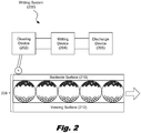
- Fig. 2 is a diagram showing an illustrative external electronic imaging substrate writing system (200).
- the electronic imaging substrate (208) moves in relation to the writing system (200).
- the writing system (200) includes a clearing device (202), a writing device (204), and a discharge device (206).
- the clearing device (202) is used to erase any images that are currently being displayed on the electronic imaging substrate (208).
- the clearing device (208) is configured to set each image cell so that it displays a white color to a human viewer.
- the clearing device (202) is an electrode that comes into close contact or is dragged along the surface of the electronic imaging substrate. The electrode may be positively charged and thus the negatively charged black particles within the image cells will be drawn towards the electrode while the positively charged white particles within the image cells will be repelled towards the viewer.
- the clearing device (202) causes the surface of the electronic imaging substrate (208) to display a white color.
- the substrate (208) will pass beneath the writing device (204).
- the writing device (204) is an ion head configured to project charged particles onto the backside surface of the electronic imaging substrate (208).
- the backside surface refers to the side opposing the side seen by a human viewer.
- the side seen by a human viewer will be referred to as the viewing surface (212).
- the backside surface (210) includes a protective layer to prevent stray electric charges from adversely affecting the image printed onto the electronic imaging substrate (208).
- the oils resulting from human contact may include charges that may distort the image printed onto the substrate (208).
- the protective layer can be designed so that the charged particles from the writing device (204) are able to get through in order to change the state of the image cells while preventing stray charges from affecting those image cells.
- the protective layer may include a porous dielectric material. This porous dielectric material may be designed so that only the writing device may be able to project charges through the backside surface (210) in a manner that will effectively rewrite the image on the electronic imaging substrate (208). Thus, it will be extremely difficult for someone to rewrite the electronic imaging substrate on their own as they will likely not have access to the proper writing equipment.
- a writing device (204) such as an ion head projects negatively charged ions onto the backside surface of the electronic imaging substrate (208). This will attract the positively charged white particles towards the backside surface and repel the negatively charged black particles towards the viewing surface.
- the writing device is configured to selectively project the negatively charged ions at certain regions in order to form the desired image as the electronic imaging substrate (208) passes.
- the writing system (200) includes a discharge device (206).
- the discharge device (206) is configured to remove any excess ions from the backside surface of the electronic imaging substrate.
- the discharge device may be a rubber conductor to collect both positively and negatively charged particles from the backside surface. If these excess charged particles were to remain on the backside surface, it is possible that they may be redistributed by regular human handling of the electronic imaging substrate. This redistribution of charged particles may cause distortion of the printed image. Thus, by removing these excess charged particles, image distortion becomes less likely.
- the electronic imaging substrate In order to print an image onto the electronic imaging substrate using such a writing system (200), the electronic imaging substrate remains a specified distance from the writing device (204) in order to provide for a smoother and quicker writing process. However, as mentioned above, this distance leads to an undesired blooming effect.
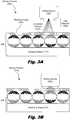
- Fig. 3A is a diagram showing an illustrative writing process (300) with a relatively wide gap between the writing device (302) and the electronic imaging substrate (208).
- the gap distance (306) between the writing device (302) and the backside surface of the electronic imaging substrate (208) leads to the blooming effect.
- a buildup of those charged particles forms on the backside surface.
- Fig. 3B is a diagram showing an illustrative writing process with a relatively small gap between the writing device and the electronic imaging substrate.
- the blooming effect can be reduced by moving the writing device (302) closer to the electronic imaging substrate (208). This is because a closer gap can allow for a stronger electric field between the writing device (302) and the substrate (208). The reasons for this will be discussed in greater detail below with the text accompanying Fig. 6 .
- This stronger electric field allows for a more focused projection of charged particles towards the electronic imaging substrate (208).
- This focused projection makes it more likely that only image cells intended to be rewritten are affected by the writing device (302). This, in turn, provides for a finer resolution to be printed onto the electronic imaging substrate (208).
- the writing device (302) may make contact with the electronic imaging substrate (208). Although this slows down or limits the ability of the electronic imaging substrate (208) to move smoothly in relation to the writing device (302), the printing resolution can be greatly enhanced. This is because by bringing the writing device within closer proximity to the electronic imaging substrate (208), the blooming effect is reduced.
- the protective layer (308) such as a porous dielectric layer, may act as a spacer between the writing device (302) and the electronic imaging substrate (208). The thickness of the spacer may be designed so that when the writing device (302) makes contact with the substrate (208), the distance between the substrate (208) and the writing device is the desired distance in order to reduce the blooming effect past a predefined threshold.
- Figs. 4A - 4B are diagrams showing the illustrative operation of writing to an electronic imaging substrate by sliding a writing device along the surface of the substrate.
- the writing device (408) may make direct contact with the electronic imaging substrate (402).
- the writing device (408) may make direct contact with the porous dielectric material.
- the electronic imaging substrate (402) moves in relation to the writing device (408).
- a mechanical system that includes a motor, may be used to move the writing device in relation to the electronic imaging substrate.
- the writing device (402), or spacers connected to the writing device (408) will slide along the surface of the electronic imaging substrate (402).
- the material of these spacers and electronic imaging substrate (402) may be such that frictional forces are minimized.
- Fig. 4A illustrates the writing device (408) passing over a first region (404) while Fig. 4B illustrates the writing device (408) passing over a second region (406). This process continues for all regions within the electronic imaging substrate that are to be changed. While passing between the first region (404) and the second region (406), the writing device (408) is essentially dragged across the surface of the electronic imaging substrate (402).
- Figs 5A - 5C are diagrams showing the illustrative operation of writing to an electronic imaging substrate (502) with the writing device (508) coming into close contact with the substrate (502).
- Fig. 5A is a diagram showing the electronic imaging substrate (502) as it moves in relation to the writing device (508) until the writing device (508) is directly above a particular region (504) that is to be written to by the writing device (508).
- the gap between the two is such that the substrate (502) can move with ease.
- the substrate may move while maintaining a distance of approximately 250 micrometers ( ⁇ m) from the writing device (508).
- the region to which the writing device will change the state of one or more image cells comes beneath the writing device, the movement will stop.
- the substrate (502) may then be moved closer to the writing device for the writing operation.
- Fig. 4B illustrates the writing device in close proximity to the electronic imaging substrate (502).
- the mechanisms which move the substrate (502) in relation to the writing device (508) may be configured to move the substrate close enough to the writing device so that the blooming effect is reduced to a predefined threshold level.
- the design specification may call for a particular resolution. In order to achieve this resolution, the blooming effect will have to be reduced below a certain level. This certain level can be determined based on various characteristics of the writing device (508), the electronic imaging substrate (502), and any protective layer which may be placed between the substrate (502) and the writing device (508). In some cases, the writing device (508) may make contact with the substrate (502).
- the writing device (508) can perform its function in order to change the state of the one or more image cells within the region (504). As described above, the writing device (508) may project charged ions onto the substrate (502) so that the particles within the image cells are oriented appropriately to form the desired image. Upon completing the writing process at the particular region (504), the substrate may be moved back away from the writing device (508). After moving away, the substrate (502) may continue its movement in relation to the writing device (508) so that the writing device (508) will be placed above a subsequent region (506) to which to print.
- Fig. 5C is a diagram illustrative the electronic imaging substrate (502) after it has moved to a subsequent region (506) that is to be written to by the writing device (508). The process thus continues for each region within the imaging substrate that is to be written to by the writing device (508). As mentioned above, the process of reducing the gap between the substrate (502) and the writing device (508) for each region will take more time. However, this extra time is not so much that it has an adverse affect for most applications. For example, if the electronic imaging substrate is a strip on a handheld card to be rewritten after a purchase, the card holder most likely does not care if the process takes a few seconds as opposed to a few microseconds.
- Fig. 6 is a graph (600) showing an illustrative relationship between gap distance and electrical field breakdown.
- the vertical axis represents the electric field breakdown (602). In one example, the electric field breakdown is measured in volts per micrometer (V/ ⁇ m).
- the horizontal axis represents the gap distance (604) between the writing device and the surface of the electronic imaging substrate.
- the graph (600) shows that as the gap increases, the electric field breakdown also increases. A higher electric field breakdown means that it will take more volts per micrometer to cause an electric field breakdown.
- An electric field breakdown occurs when the voltage potential across a dielectric material is high enough so that the electric field breaks down and the dielectric loses its insulating characteristics. Thus, current will flow through dielectric when the electric field breaks down. For example, if the dielectric is air and a voltage is applied between two points, there is a point when the voltage potential is such that an electric current will flow in the form of an arc through the air.
- the electric field breakdown in air may be affected by a variety of factors such as temperature, pressure, and humidity.
- Fig. 7 is a diagram showing an illustrative handheld card (700) having an electronic imaging substrate formed within.
- an electronic imaging substrate strip (702) may be embedded within a handheld sized card.
- the handheld sized card (700) may be approximately the size of a credit card.
- the card (700) may be made of a plastic card material (706) except for the region that includes the electronic imaging substrate strip (702).
- Such a handheld card maybe used for a variety of applications.
- the card may be used as a security access card.
- a writing device may write text or images (704) onto the electronic imaging substrate strip.
- the text may indicate the time and date of entry while the images may include various logos that change by the day and that security personnel will recognize.
- such a handheld card may be used as a gift card.
- the card may have an initial balance printed onto the electronic imaging substrate strip (702).
- the new balance may be rewritten by a writing device used by the retailer.
- various logos or advertisements may be rewritten onto the electronic imaging substrate strips of the cards as customers use the card (700).
- Fig. 8 is a flowchart showing an illustrative method for writing to an electronic imaging substrate.
- the method includes passing (block 802) an electronic imaging substrate by a writing device to change a state of an image cell within the electronic imaging substrate and stopping (block 804) a movement of the electronic imaging substrate in relation to the writing device to change the state of the image cell.
- the electronic imaging substrate is placed close enough to the writing device when being stopped so as to reduce a blooming effect to a predefined threshold level.
- the method further includes moving (block 806) the electronic imaging substrate in relation to the writing device so that a state of a subsequent image cell is in position to be changed by the writing device.
Claims (13)
- Elektronisches Bildgebungssubstratschreibsystem, Folgendes umfassend:eine Schreibvorrichtung (204; 302; 408; 508), umfassend einen Ionenkopf zum Erzeugen eines lonenstrahls zum Ändern eines Zustands einer Bildzelle (100) innerhalb eines elektronischen Bildgebungssubstrats (110; 208; 402; 502) in einem Schreibvorgang; undgekennzeichnet durch Umfassen eines mechanischen Systems, welches während des Gebrauchs des Substratschreibsystems:die Schreibvorrichtung (204; 302; 408; 508) mit Bezug auf das elektronische Bildgebungssubstrat (110; 208; 402; 502) bewegt, um die Schreibvorrichtung (204; 302; 408; 508) mit Bezug auf das Substrat mit einer ersten Spalte dazwischen zu passieren, bis die Schreibvorrichtung (204; 302; 408; 508) sich oberhalb eines Bereichs befindet, auf den mit der Schreibvorrichtung (204; 302; 408; 508) geschrieben werden soll; undden Spalt zwischen dem elektronischen Bildgebungssubstrat (110; 208; 402; 502) und der Schreibvorrichtung (204; 302; 408; 508) für den Schreibvorgang verringert, wenn sich die Schreibvorrichtung (204; 302; 408; 508) oberhalb des Bereichs befindet.
- System nach Anspruch 1, wobei die Schreibvorrichtung (204; 302; 408; 508) ferner eine Bewegung des elektronischen Bildgebungssubstrats (110; 208; 402; 502), das mit Bezug auf die Schreibvorrichtung (204; 302; 408; 508) passiert, anhält, wenn die Schreibvorrichtung (204; 302; 408; 508) einen Zustand der Bildzelle (100) verändert.
- System nach Anspruch 2, wobei die Schreibvorrichtung (204; 302; 408; 508) eine Oberfläche (210) des elektronischen Bildgebungssubstrats (110; 208; 402; 502) beim Ändern eines Zustands einer der Bildzellen (100) berührt.
- System nach Anspruch 1, wobei das elektronische Bildgebungssubstrat (110; 208; 402; 502) ein poröses Dielektrikum auf einer Seite des elektronischen Bildgebungssubstrats (110; 208; 402; 502) umfasst, zur Schreibvorrichtung (204; 302; 408; 508) hin angeordnet, wobei das poröse Dielektrikum als ein Abstandhalter zwischen der Schreibvorrichtung (204; 302; 408; 508) und dem elektronischen Bildgebungssubstrat (110; 208; 402; 502) wirkt.
- System nach Anspruch 1, wobei das elektronische Bildgebungssubstrat (110; 208; 402; 502) in einer Karte (700) von tragbarer Größe eingebettet ist.
- System nach Anspruch 5, wobei das elektronische Bildgebungssubstrat einen Streifen in der Karte (702) ausbildet.
- Verfahren zum Schreiben auf ein elektronisches Bildgebungssubstrat (110; 208; 402; 502), wobei das Verfahren Folgendes umfasst:Passieren eines elektronischen Bildgebungssubstrats (110; 208; 402; 502) mit Bezug auf eine Schreibvorrichtung (204; 302; 408; 508), umfassend einen Ionenkopf zum Erzeugen eines lonenstrahls zum Ändern eines Zustands von Bildzellen (100) innerhalb des elektronischen Bildgebungssubstrats (110; 208; 402; 502) in einem Schreibvorgang; unddadurch gekennzeichnet, dass, wenn sich die Schreibvorrichtung (204; 302; 408; 508) oberhalb eines Bereichs befindet, auf den die Schreibvorrichtung (204; 302; 408; 508) schreiben soll, das Verfahren das Bewegen des elektronischen Bildgebungssubstrats (110; 208; 402; 502) näher zu der Schreibvorrichtung (204; 302; 408; 508) für den Schreibvorgang umfasst.
- Verfahren nach Anspruch 7, ferner Folgendes umfassend: Anhalten einer Bewegung des elektronischen Bildgebungssubstrats (110; 208; 402; 502) mit Bezug auf die Schreibvorrichtung (204; 302; 408; 508), wenn die Schreibvorrichtung (204; 302; 408; 508) einen Zustand einer der Bildzellen (100) verändert.
- Verfahren nach Anspruch 8, wobei die Schreibvorrichtung (204; 302; 408; 508) eine Oberfläche des elektronischen Bildgebungssubstrats (110; 208; 402; 502) beim Ändern eines Zustands einer der Bildzellen (100) berührt.
- Verfahren nach Anspruch 7, wobei das elektronische Bildgebungssubstrat (110; 208; 402; 502) ein poröses Dielektrikum auf einer Seite des elektronischen Bildgebungssubstrats umfasst, zur Schreibvorrichtung (204; 302; 408; 508) hin angeordnet, wobei das poröse Dielektrikum als ein Abstandhalter zwischen der Schreibvorrichtung und dem elektronischen Bildgebungssubstrat (110; 208; 402; 502) wirkt.
- Verfahren nach Anspruch 7, wobei das elektronische Bildgebungssubstrat (110; 208; 402; 502) in einer Karte (700) von tragbarer Größe eingebettet ist.
- Verfahren nach Anspruch 11, wobei das elektronische Bildgebungssubstrat einen Streifen (702) in der Karte (700) ausbildet.
- Verfahren nach Anspruch 7 zum Bedrucken eines elektronischen Bildgebungssubstrats (110; 208; 402; 502), wobei das Verfahren Folgendes umfasst:Anhalten einer Bewegung des elektronischen Bildgebungssubstrats (110; 208; 402; 502) mit Bezug auf die Schreibvorrichtung (204; 302; 408; 508), um den Zustand der Bildzelle (100) zu verändern;Bewegen des elektronischen Bildgebungssubstrats (110; 208; 402; 502) weg von der Schreibvorrichtung (204; 302; 408; 508);Bewegen des elektronischen Bildgebungssubstrats (110; 208; 402; 502) mit Bezug auf die Schreibvorrichtung (204; 302; 408; 508), sodass eine darauffolgende Bildzelle (100) sich in Position befindet, um durch die Schreibvorrichtung (204; 302; 408; 508) geändert zu werden; und,wenn sich die Schreibvorrichtung (204; 302; 408; 508) oberhalb der darauffolgenden Zelle befindet; Bewegen des elektronischen Bildgebungssubstrats (204; 302; 408; 508) näher zu der Schreibvorrichtung (204; 302; 408; 508) für den Schreibvorgang.
Applications Claiming Priority (1)
| Application Number | Priority Date | Filing Date | Title |
|---|---|---|---|
| PCT/US2011/057131 WO2013058757A1 (en) | 2011-10-20 | 2011-10-20 | Writing to an electronic imaging substrate |
Publications (3)
| Publication Number | Publication Date |
|---|---|
| EP2769264A1 EP2769264A1 (de) | 2014-08-27 |
| EP2769264A4 EP2769264A4 (de) | 2016-01-06 |
| EP2769264B1 true EP2769264B1 (de) | 2017-08-16 |
Family
ID=48141209
Family Applications (1)
| Application Number | Title | Priority Date | Filing Date |
|---|---|---|---|
| EP11874298.0A Active EP2769264B1 (de) | 2011-10-20 | 2011-10-20 | Schreibvorgänge auf einem elektronischen abbildungssubstrat |
Country Status (4)
| Country | Link |
|---|---|
| US (1) | US10000074B2 (de) |
| EP (1) | EP2769264B1 (de) |
| JP (1) | JP5902819B2 (de) |
| WO (1) | WO2013058757A1 (de) |
Families Citing this family (21)
| Publication number | Priority date | Publication date | Assignee | Title |
|---|---|---|---|---|
| US20110298760A1 (en) | 2010-06-02 | 2011-12-08 | Omer Gila | Systems and methods for writing on and using electronic paper |
| JP5902819B2 (ja) | 2011-10-20 | 2016-04-13 | ヒューレット−パッカード デベロップメント カンパニー エル.ピー.Hewlett‐Packard Development Company, L.P. | 電子イメージング基体への書き込み |
| WO2015099672A1 (en) | 2013-12-23 | 2015-07-02 | Hewlett-Packard Development Company, L.P. | Writing information on substrate displays |
| WO2015116212A2 (en) | 2014-01-31 | 2015-08-06 | Hewlett-Packard Development Company, L.P. | Display device |
| WO2015116214A2 (en) | 2014-01-31 | 2015-08-06 | Hewlett-Packard Development Company, L.P. | E-paper display media |
| WO2015116213A1 (en) | 2014-01-31 | 2015-08-06 | Hewlett-Packard Development Company, L.P. | Media with recessed e-paper display |
| WO2015116211A1 (en) | 2014-01-31 | 2015-08-06 | Hewlett-Packard Development Company, L.P. | Display device |
| EP3100255B1 (de) | 2014-01-31 | 2019-03-06 | Hewlett-Packard Development Company, L.P. | Schreiber für e-paper-anzeige |
| EP3100110B1 (de) | 2014-01-31 | 2019-07-03 | Hewlett-Packard Development Company, L.P. | Mobile bildgebungsvorrichtung |
| WO2015116226A1 (en) | 2014-01-31 | 2015-08-06 | Hewlett-Packard Development Company, L.P. | E-paper imaging via addressable electrode array |
| US10649302B2 (en) | 2014-04-25 | 2020-05-12 | Hewlett-Packard Development Company, L.P. | Aligned particle coating |
| EP3134769B1 (de) | 2014-04-25 | 2020-08-19 | Hewlett-Packard Development Company, L.P. | Ausgerichtete partikelschicht |
| CN106687879B (zh) | 2014-07-29 | 2020-03-27 | 惠普发展公司,有限责任合伙企业 | 显示设备 |
| WO2016018257A1 (en) | 2014-07-29 | 2016-02-04 | Hewlett-Packard Development Company, L.P. | Display device |
| JP6368861B2 (ja) | 2014-07-30 | 2018-08-01 | ヒューレット−パッカード デベロップメント カンパニー エル.ピー.Hewlett‐Packard Development Company, L.P. | 空気流を有するイオン書き込みユニット |
| US10579161B2 (en) | 2014-07-31 | 2020-03-03 | Hewlett-Packard Development Company, L.P. | ION writing calibration |
| WO2016068924A1 (en) | 2014-10-30 | 2016-05-06 | Hewlett-Packard Development Company, L.P. | Transaction medium |
| CN108351568B (zh) | 2015-10-28 | 2022-01-25 | 惠普发展公司,有限责任合伙企业 | 无源电子纸成像 |
| US10460160B2 (en) * | 2015-10-29 | 2019-10-29 | Hewlett-Packard Development Company, L.P. | E-paper imager |
| EP3622440A4 (de) | 2017-07-24 | 2020-12-30 | Hewlett-Packard Development Company, L.P. | Bildgebung mit auftragsticket |
| CN108803188B (zh) * | 2018-08-30 | 2021-05-11 | 京东方科技集团股份有限公司 | 一种像素结构、其驱动方法、电子纸及显示装置 |
Citations (1)
| Publication number | Priority date | Publication date | Assignee | Title |
|---|---|---|---|---|
| US5225856A (en) * | 1991-12-23 | 1993-07-06 | Xerox Corporation | Method and apparatus for correction of blooming artifacts in ionographic devices |
Family Cites Families (65)
| Publication number | Priority date | Publication date | Assignee | Title |
|---|---|---|---|---|
| US4558334A (en) * | 1983-06-06 | 1985-12-10 | Fotland Richard A | Electrostatic imaging device |
| US4816653A (en) | 1986-05-16 | 1989-03-28 | American Telephone And Telegraph Company | Security file system for a portable data carrier |
| US4972212A (en) | 1989-06-22 | 1990-11-20 | Xerox Corporation | Method and apparatus for controlling ion trajectory perturbations in ionographic devices |
| JPH07179060A (ja) | 1993-12-23 | 1995-07-18 | Ricoh Co Ltd | カード処理方法 |
| ATE209366T1 (de) | 1996-03-15 | 2001-12-15 | Ecole Polytech | Elektrochrome oder photoelektrochrome vorrichtung |
| US5866284A (en) | 1997-05-28 | 1999-02-02 | Hewlett-Packard Company | Print method and apparatus for re-writable medium |
| JPH1110936A (ja) | 1997-06-27 | 1999-01-19 | Hitachi Ltd | イオンフロー記録装置 |
| US6222513B1 (en) | 1998-03-10 | 2001-04-24 | Xerox Corporation | Charge retention islands for electric paper and applications thereof |
| US7207477B1 (en) | 2004-03-08 | 2007-04-24 | Diebold, Incorporated | Wireless transfer of account data and signature from hand-held device to electronic check generator |
| AU3987299A (en) | 1998-05-12 | 1999-11-29 | E-Ink Corporation | Microencapsulated electrophoretic electrostatically-addressed media for drawing device applications |
| JP3532415B2 (ja) | 1998-07-06 | 2004-05-31 | シャープ株式会社 | 情報記録装置 |
| US6753830B2 (en) | 1998-09-11 | 2004-06-22 | Visible Tech-Knowledgy, Inc. | Smart electronic label employing electronic ink |
| JP3726646B2 (ja) | 1999-07-21 | 2005-12-14 | 富士ゼロックス株式会社 | 画像表示方法、画像表示装置、及び画像表示媒体 |
| JP2001056653A (ja) * | 1999-06-11 | 2001-02-27 | Ricoh Co Ltd | 電気泳動表示用表示液、表示粒子及び、それらを利用した表示媒体、表示装置、表示方法、表示カード、記録シート、ディスプレイ、可逆表示型看板 |
| JP4126851B2 (ja) * | 1999-07-21 | 2008-07-30 | 富士ゼロックス株式会社 | 画像表示媒体、画像形成方法、及び画像形成装置 |
| US6456272B1 (en) | 1999-11-12 | 2002-09-24 | Xerox Corporation | Field addressed displays using charge discharging in conjunction with charge retaining island structures |
| US6573880B1 (en) | 1999-11-16 | 2003-06-03 | Xerox Corporation | Applications for electronic reusable paper |
| US6515790B2 (en) | 2000-01-28 | 2003-02-04 | Minolta Co., Ltd. | Reversible image display medium and image display method |
| US20020021911A1 (en) * | 2000-06-09 | 2002-02-21 | Masahiko Matsuura | Image forming apparatus |
| JP2002174827A (ja) * | 2000-12-05 | 2002-06-21 | Minolta Co Ltd | 可逆性画像表示媒体 |
| JP2002350905A (ja) * | 2001-05-25 | 2002-12-04 | Minolta Co Ltd | 画像表示媒体及び画像表示方法 |
| US6795228B2 (en) | 2001-12-17 | 2004-09-21 | Xerox Corporation | Display material for electric paper and applications thereof |
| US7479942B2 (en) | 2003-06-25 | 2009-01-20 | Xerox Corporation | Stylus writing architectures for erasable paper |
| US6982734B2 (en) | 2003-10-06 | 2006-01-03 | Hewlett-Packard Development Company, L.P. | Printing on electrically writable media and electrically writable displays |
| US7355783B2 (en) | 2003-12-18 | 2008-04-08 | Xerox Corporation | Printer wiper for printing on bichromal or multi-colored electronic paper |
| US7265894B2 (en) | 2003-12-18 | 2007-09-04 | Xerox Corporation | Bi-directional printer wiper for printing on bichromal or multi-colored electronic paper |
| GB2422808C (en) | 2004-03-11 | 2008-05-23 | Fukuoka Technoken Kogyo Co Ltd | Print head and image forming apparatus including the same. |
| US7580845B2 (en) | 2004-04-13 | 2009-08-25 | United Parcel Services Of America, Inc. | Electronic shipping label with updateable visual display |
| US20060017659A1 (en) * | 2004-04-28 | 2006-01-26 | Matsushita Electric Industrial Co., Ltd. | Electronic paper display system |
| JP2006035478A (ja) * | 2004-07-23 | 2006-02-09 | Matsushita Electric Ind Co Ltd | 処理装置および処理システム |
| JP2005326543A (ja) * | 2004-05-13 | 2005-11-24 | Matsushita Electric Ind Co Ltd | シート媒体およびそれを用いた通信端末装置 |
| JP4096315B2 (ja) | 2004-08-04 | 2008-06-04 | セイコーエプソン株式会社 | 表示システム |
| US7321356B2 (en) | 2004-12-15 | 2008-01-22 | Palo Alto Research Center Incorporated | Time domain printing for electric paper |
| US8102362B2 (en) * | 2005-02-01 | 2012-01-24 | Industrial Technology Research Institute | Indexing writehead for bistable media |
| US8820637B1 (en) * | 2005-02-26 | 2014-09-02 | James A. Roskind | Time-varying security code for enabling authorizations and other uses of financial accounts |
| US7284708B2 (en) * | 2005-08-23 | 2007-10-23 | Xerox Corporation | Card with rewriteable display |
| US7855711B2 (en) | 2005-09-14 | 2010-12-21 | Palo Alto Research Center Incorporated | Conductive islands for printable electronic paper |
| JP4894285B2 (ja) | 2006-02-10 | 2012-03-14 | 富士ゼロックス株式会社 | 画像表示媒体、及びそれを備える画像表示装置 |
| JP2007212978A (ja) | 2006-02-13 | 2007-08-23 | Fuji Xerox Co Ltd | エレクトロクロミック表示素子 |
| WO2008065605A2 (en) | 2006-11-30 | 2008-06-05 | Koninklijke Philips Electronics N.V. | In-plane switching electrophoretic colour display |
| JP2008149498A (ja) * | 2006-12-14 | 2008-07-03 | Fukuoka Technoken Kogyo:Kk | 画像形成方法 |
| KR100860800B1 (ko) | 2007-01-05 | 2008-09-29 | 주식회사 제이디씨텍 | 카드로고가 점등되는 스마트 카드 |
| JP4407699B2 (ja) | 2007-02-02 | 2010-02-03 | セイコーエプソン株式会社 | 表示装置及び電子ペーパー |
| WO2008103451A1 (en) | 2007-02-22 | 2008-08-28 | Karen Nixon-Lane | Segmented microencapsulated display system |
| CN101681537A (zh) | 2007-04-06 | 2010-03-24 | 路易吉·莫迪卡 | 用于显示可充值信用卡余额的装置 |
| US7875307B2 (en) | 2007-05-25 | 2011-01-25 | Xerox Corporation | Method for forming an electronic paper display |
| KR20080109408A (ko) | 2007-06-13 | 2008-12-17 | 엘지디스플레이 주식회사 | 정보 표시카드 |
| US7975927B1 (en) | 2007-07-16 | 2011-07-12 | Cecile Whitney | Electronic transaction card |
| KR20110004907A (ko) * | 2008-06-10 | 2011-01-14 | 다이셀 가가꾸 고교 가부시끼가이샤 | 다공질층을 갖는 적층체 및 그것을 사용한 기능성 적층체 |
| JP2010046848A (ja) | 2008-08-20 | 2010-03-04 | Kobayashi Create Co Ltd | イオンフロー記録ヘッド |
| JP2010069732A (ja) | 2008-09-18 | 2010-04-02 | Kobayashi Create Co Ltd | イオンフロー記録ヘッド |
| JP5540851B2 (ja) | 2009-06-04 | 2014-07-02 | セイコーエプソン株式会社 | 表示装置および表示シート |
| US20110060640A1 (en) | 2009-09-04 | 2011-03-10 | American Express Travel Related Services Co., Inc. | System, method and apparatus for providing messages to a transaction instrument |
| US8261998B2 (en) | 2009-11-03 | 2012-09-11 | American Express Travel Related Services Company, Inc. | Customizable transaction card |
| US8514256B2 (en) | 2010-02-04 | 2013-08-20 | Seiko Epson Corporation | Device and method for recording image to electronic paper |
| US9104082B2 (en) | 2011-06-29 | 2015-08-11 | Hewlett-Packard Development Company, L.P. | Electronic paper with porous standoff layer |
| US8830160B2 (en) | 2010-06-02 | 2014-09-09 | Hewlett-Packard Development Company, L.P. | Presenting information on a card with a passive electronic paper display |
| US20110298760A1 (en) * | 2010-06-02 | 2011-12-08 | Omer Gila | Systems and methods for writing on and using electronic paper |
| US9305496B2 (en) | 2010-07-01 | 2016-04-05 | Semiconductor Energy Laboratory Co., Ltd. | Electric field driving display device |
| KR101260013B1 (ko) | 2011-04-29 | 2013-05-06 | 인텔렉추얼디스커버리 주식회사 | 전자 종이용 데이터 기록 장치 및 이를 이용한 데이터 기록 방법 |
| US8493319B2 (en) | 2011-06-15 | 2013-07-23 | Hewlett-Packard Development Company, L.P. | Electronic paper with semiconducting coating |
| JP5902819B2 (ja) | 2011-10-20 | 2016-04-13 | ヒューレット−パッカード デベロップメント カンパニー エル.ピー.Hewlett‐Packard Development Company, L.P. | 電子イメージング基体への書き込み |
| US8542429B1 (en) | 2012-03-09 | 2013-09-24 | Hewlett-Packard Development Company, L.P. | Techniques for protecting imaging access of electronic paper |
| US8941636B2 (en) | 2013-01-31 | 2015-01-27 | Hewlett-Packard Development Company, L.P. | E-paper printing system |
| US20140239068A1 (en) | 2013-02-22 | 2014-08-28 | John Chowhan Park | Credit card with alterable id/security features |
-
2011
- 2011-10-20 JP JP2014537039A patent/JP5902819B2/ja not_active Expired - Fee Related
- 2011-10-20 EP EP11874298.0A patent/EP2769264B1/de active Active
- 2011-10-20 US US14/349,919 patent/US10000074B2/en active Active
- 2011-10-20 WO PCT/US2011/057131 patent/WO2013058757A1/en active Application Filing
Patent Citations (1)
| Publication number | Priority date | Publication date | Assignee | Title |
|---|---|---|---|---|
| US5225856A (en) * | 1991-12-23 | 1993-07-06 | Xerox Corporation | Method and apparatus for correction of blooming artifacts in ionographic devices |
Also Published As
| Publication number | Publication date |
|---|---|
| JP5902819B2 (ja) | 2016-04-13 |
| WO2013058757A1 (en) | 2013-04-25 |
| US20140253426A1 (en) | 2014-09-11 |
| EP2769264A1 (de) | 2014-08-27 |
| EP2769264A4 (de) | 2016-01-06 |
| JP2014533374A (ja) | 2014-12-11 |
| US10000074B2 (en) | 2018-06-19 |
Similar Documents
| Publication | Publication Date | Title |
|---|---|---|
| EP2769264B1 (de) | Schreibvorgänge auf einem elektronischen abbildungssubstrat | |
| US8493319B2 (en) | Electronic paper with semiconducting coating | |
| US11390091B2 (en) | Writing electronic paper | |
| US9046733B2 (en) | E-paper printing system | |
| US11644732B2 (en) | Display device | |
| EP3100108B1 (de) | E-papier-anzeigemedien | |
| US9846493B2 (en) | Systems and methods for writing on and using electronic paper | |
| US7479942B2 (en) | Stylus writing architectures for erasable paper | |
| US10559268B2 (en) | Passive e-paper imaging and erasing | |
| TWI621901B (zh) | 顯示器裝置 | |
| US10288972B2 (en) | Display device | |
| CN108351566B (zh) | 显示设备 | |
| US7671834B2 (en) | Electric writable media | |
| JP3946378B2 (ja) | 書込装置 | |
| CA3103687A1 (en) | Piezo electrophoretic display |
Legal Events
| Date | Code | Title | Description |
|---|---|---|---|
| PUAI | Public reference made under article 153(3) epc to a published international application that has entered the european phase |
Free format text: ORIGINAL CODE: 0009012 |
|
| 17P | Request for examination filed |
Effective date: 20140320 |
|
| AK | Designated contracting states |
Kind code of ref document: A1 Designated state(s): AL AT BE BG CH CY CZ DE DK EE ES FI FR GB GR HR HU IE IS IT LI LT LU LV MC MK MT NL NO PL PT RO RS SE SI SK SM TR |
|
| DAX | Request for extension of the european patent (deleted) | ||
| RA4 | Supplementary search report drawn up and despatched (corrected) |
Effective date: 20151204 |
|
| RIC1 | Information provided on ipc code assigned before grant |
Ipc: B41J 3/407 20060101ALI20151130BHEP Ipc: G02F 1/167 20060101AFI20151130BHEP |
|
| 17Q | First examination report despatched |
Effective date: 20160630 |
|
| REG | Reference to a national code |
Ref country code: DE Ref legal event code: R079 Ref document number: 602011040737 Country of ref document: DE Free format text: PREVIOUS MAIN CLASS: G02F0001167000 Ipc: G09G0003340000 |
|
| GRAP | Despatch of communication of intention to grant a patent |
Free format text: ORIGINAL CODE: EPIDOSNIGR1 |
|
| RIC1 | Information provided on ipc code assigned before grant |
Ipc: B41J 3/407 20060101ALI20170130BHEP Ipc: G09G 3/34 20060101AFI20170130BHEP Ipc: G02F 1/167 20060101ALI20170130BHEP |
|
| INTG | Intention to grant announced |
Effective date: 20170215 |
|
| GRAS | Grant fee paid |
Free format text: ORIGINAL CODE: EPIDOSNIGR3 |
|
| GRAJ | Information related to disapproval of communication of intention to grant by the applicant or resumption of examination proceedings by the epo deleted |
Free format text: ORIGINAL CODE: EPIDOSDIGR1 |
|
| GRAL | Information related to payment of fee for publishing/printing deleted |
Free format text: ORIGINAL CODE: EPIDOSDIGR3 |
|
| GRAR | Information related to intention to grant a patent recorded |
Free format text: ORIGINAL CODE: EPIDOSNIGR71 |
|
| GRAA | (expected) grant |
Free format text: ORIGINAL CODE: 0009210 |
|
| INTC | Intention to grant announced (deleted) | ||
| AK | Designated contracting states |
Kind code of ref document: B1 Designated state(s): AL AT BE BG CH CY CZ DE DK EE ES FI FR GB GR HR HU IE IS IT LI LT LU LV MC MK MT NL NO PL PT RO RS SE SI SK SM TR |
|
| INTG | Intention to grant announced |
Effective date: 20170712 |
|
| REG | Reference to a national code |
Ref country code: GB Ref legal event code: FG4D |
|
| REG | Reference to a national code |
Ref country code: CH Ref legal event code: EP |
|
| REG | Reference to a national code |
Ref country code: IE Ref legal event code: FG4D |
|
| REG | Reference to a national code |
Ref country code: AT Ref legal event code: REF Ref document number: 919791 Country of ref document: AT Kind code of ref document: T Effective date: 20170915 |
|
| REG | Reference to a national code |
Ref country code: FR Ref legal event code: PLFP Year of fee payment: 7 |
|
| REG | Reference to a national code |
Ref country code: DE Ref legal event code: R096 Ref document number: 602011040737 Country of ref document: DE |
|
| REG | Reference to a national code |
Ref country code: NL Ref legal event code: MP Effective date: 20170816 |
|
| REG | Reference to a national code |
Ref country code: LT Ref legal event code: MG4D |
|
| REG | Reference to a national code |
Ref country code: AT Ref legal event code: MK05 Ref document number: 919791 Country of ref document: AT Kind code of ref document: T Effective date: 20170816 |
|
| PG25 | Lapsed in a contracting state [announced via postgrant information from national office to epo] |
Ref country code: LT Free format text: LAPSE BECAUSE OF FAILURE TO SUBMIT A TRANSLATION OF THE DESCRIPTION OR TO PAY THE FEE WITHIN THE PRESCRIBED TIME-LIMIT Effective date: 20170816 Ref country code: NL Free format text: LAPSE BECAUSE OF FAILURE TO SUBMIT A TRANSLATION OF THE DESCRIPTION OR TO PAY THE FEE WITHIN THE PRESCRIBED TIME-LIMIT Effective date: 20170816 Ref country code: NO Free format text: LAPSE BECAUSE OF FAILURE TO SUBMIT A TRANSLATION OF THE DESCRIPTION OR TO PAY THE FEE WITHIN THE PRESCRIBED TIME-LIMIT Effective date: 20171116 Ref country code: FI Free format text: LAPSE BECAUSE OF FAILURE TO SUBMIT A TRANSLATION OF THE DESCRIPTION OR TO PAY THE FEE WITHIN THE PRESCRIBED TIME-LIMIT Effective date: 20170816 Ref country code: SE Free format text: LAPSE BECAUSE OF FAILURE TO SUBMIT A TRANSLATION OF THE DESCRIPTION OR TO PAY THE FEE WITHIN THE PRESCRIBED TIME-LIMIT Effective date: 20170816 Ref country code: AT Free format text: LAPSE BECAUSE OF FAILURE TO SUBMIT A TRANSLATION OF THE DESCRIPTION OR TO PAY THE FEE WITHIN THE PRESCRIBED TIME-LIMIT Effective date: 20170816 |
|
| PG25 | Lapsed in a contracting state [announced via postgrant information from national office to epo] |
Ref country code: IS Free format text: LAPSE BECAUSE OF FAILURE TO SUBMIT A TRANSLATION OF THE DESCRIPTION OR TO PAY THE FEE WITHIN THE PRESCRIBED TIME-LIMIT Effective date: 20171216 Ref country code: PL Free format text: LAPSE BECAUSE OF FAILURE TO SUBMIT A TRANSLATION OF THE DESCRIPTION OR TO PAY THE FEE WITHIN THE PRESCRIBED TIME-LIMIT Effective date: 20170816 Ref country code: GR Free format text: LAPSE BECAUSE OF FAILURE TO SUBMIT A TRANSLATION OF THE DESCRIPTION OR TO PAY THE FEE WITHIN THE PRESCRIBED TIME-LIMIT Effective date: 20171117 Ref country code: ES Free format text: LAPSE BECAUSE OF FAILURE TO SUBMIT A TRANSLATION OF THE DESCRIPTION OR TO PAY THE FEE WITHIN THE PRESCRIBED TIME-LIMIT Effective date: 20170816 Ref country code: RS Free format text: LAPSE BECAUSE OF FAILURE TO SUBMIT A TRANSLATION OF THE DESCRIPTION OR TO PAY THE FEE WITHIN THE PRESCRIBED TIME-LIMIT Effective date: 20170816 Ref country code: BG Free format text: LAPSE BECAUSE OF FAILURE TO SUBMIT A TRANSLATION OF THE DESCRIPTION OR TO PAY THE FEE WITHIN THE PRESCRIBED TIME-LIMIT Effective date: 20171116 Ref country code: LV Free format text: LAPSE BECAUSE OF FAILURE TO SUBMIT A TRANSLATION OF THE DESCRIPTION OR TO PAY THE FEE WITHIN THE PRESCRIBED TIME-LIMIT Effective date: 20170816 |
|
| PG25 | Lapsed in a contracting state [announced via postgrant information from national office to epo] |
Ref country code: DK Free format text: LAPSE BECAUSE OF FAILURE TO SUBMIT A TRANSLATION OF THE DESCRIPTION OR TO PAY THE FEE WITHIN THE PRESCRIBED TIME-LIMIT Effective date: 20170816 Ref country code: RO Free format text: LAPSE BECAUSE OF FAILURE TO SUBMIT A TRANSLATION OF THE DESCRIPTION OR TO PAY THE FEE WITHIN THE PRESCRIBED TIME-LIMIT Effective date: 20170816 Ref country code: CZ Free format text: LAPSE BECAUSE OF FAILURE TO SUBMIT A TRANSLATION OF THE DESCRIPTION OR TO PAY THE FEE WITHIN THE PRESCRIBED TIME-LIMIT Effective date: 20170816 |
|
| REG | Reference to a national code |
Ref country code: DE Ref legal event code: R097 Ref document number: 602011040737 Country of ref document: DE |
|
| PG25 | Lapsed in a contracting state [announced via postgrant information from national office to epo] |
Ref country code: MC Free format text: LAPSE BECAUSE OF FAILURE TO SUBMIT A TRANSLATION OF THE DESCRIPTION OR TO PAY THE FEE WITHIN THE PRESCRIBED TIME-LIMIT Effective date: 20170816 Ref country code: EE Free format text: LAPSE BECAUSE OF FAILURE TO SUBMIT A TRANSLATION OF THE DESCRIPTION OR TO PAY THE FEE WITHIN THE PRESCRIBED TIME-LIMIT Effective date: 20170816 Ref country code: SK Free format text: LAPSE BECAUSE OF FAILURE TO SUBMIT A TRANSLATION OF THE DESCRIPTION OR TO PAY THE FEE WITHIN THE PRESCRIBED TIME-LIMIT Effective date: 20170816 Ref country code: SM Free format text: LAPSE BECAUSE OF FAILURE TO SUBMIT A TRANSLATION OF THE DESCRIPTION OR TO PAY THE FEE WITHIN THE PRESCRIBED TIME-LIMIT Effective date: 20170816 Ref country code: IT Free format text: LAPSE BECAUSE OF FAILURE TO SUBMIT A TRANSLATION OF THE DESCRIPTION OR TO PAY THE FEE WITHIN THE PRESCRIBED TIME-LIMIT Effective date: 20170816 |
|
| REG | Reference to a national code |
Ref country code: CH Ref legal event code: PL |
|
| PLBE | No opposition filed within time limit |
Free format text: ORIGINAL CODE: 0009261 |
|
| STAA | Information on the status of an ep patent application or granted ep patent |
Free format text: STATUS: NO OPPOSITION FILED WITHIN TIME LIMIT |
|
| 26N | No opposition filed |
Effective date: 20180517 |
|
| REG | Reference to a national code |
Ref country code: IE Ref legal event code: MM4A |
|
| PG25 | Lapsed in a contracting state [announced via postgrant information from national office to epo] |
Ref country code: LU Free format text: LAPSE BECAUSE OF NON-PAYMENT OF DUE FEES Effective date: 20171020 Ref country code: LI Free format text: LAPSE BECAUSE OF NON-PAYMENT OF DUE FEES Effective date: 20171031 Ref country code: CH Free format text: LAPSE BECAUSE OF NON-PAYMENT OF DUE FEES Effective date: 20171031 |
|
| REG | Reference to a national code |
Ref country code: BE Ref legal event code: MM Effective date: 20171031 |
|
| PG25 | Lapsed in a contracting state [announced via postgrant information from national office to epo] |
Ref country code: BE Free format text: LAPSE BECAUSE OF NON-PAYMENT OF DUE FEES Effective date: 20171031 Ref country code: SI Free format text: LAPSE BECAUSE OF FAILURE TO SUBMIT A TRANSLATION OF THE DESCRIPTION OR TO PAY THE FEE WITHIN THE PRESCRIBED TIME-LIMIT Effective date: 20170816 |
|
| REG | Reference to a national code |
Ref country code: FR Ref legal event code: PLFP Year of fee payment: 8 |
|
| PG25 | Lapsed in a contracting state [announced via postgrant information from national office to epo] |
Ref country code: MT Free format text: LAPSE BECAUSE OF NON-PAYMENT OF DUE FEES Effective date: 20171020 |
|
| PG25 | Lapsed in a contracting state [announced via postgrant information from national office to epo] |
Ref country code: IE Free format text: LAPSE BECAUSE OF NON-PAYMENT OF DUE FEES Effective date: 20171020 |
|
| PG25 | Lapsed in a contracting state [announced via postgrant information from national office to epo] |
Ref country code: HU Free format text: LAPSE BECAUSE OF FAILURE TO SUBMIT A TRANSLATION OF THE DESCRIPTION OR TO PAY THE FEE WITHIN THE PRESCRIBED TIME-LIMIT; INVALID AB INITIO Effective date: 20111020 |
|
| PG25 | Lapsed in a contracting state [announced via postgrant information from national office to epo] |
Ref country code: CY Free format text: LAPSE BECAUSE OF NON-PAYMENT OF DUE FEES Effective date: 20170816 |
|
| PG25 | Lapsed in a contracting state [announced via postgrant information from national office to epo] |
Ref country code: MK Free format text: LAPSE BECAUSE OF FAILURE TO SUBMIT A TRANSLATION OF THE DESCRIPTION OR TO PAY THE FEE WITHIN THE PRESCRIBED TIME-LIMIT Effective date: 20170816 |
|
| PG25 | Lapsed in a contracting state [announced via postgrant information from national office to epo] |
Ref country code: TR Free format text: LAPSE BECAUSE OF FAILURE TO SUBMIT A TRANSLATION OF THE DESCRIPTION OR TO PAY THE FEE WITHIN THE PRESCRIBED TIME-LIMIT Effective date: 20170816 |
|
| PG25 | Lapsed in a contracting state [announced via postgrant information from national office to epo] |
Ref country code: PT Free format text: LAPSE BECAUSE OF FAILURE TO SUBMIT A TRANSLATION OF THE DESCRIPTION OR TO PAY THE FEE WITHIN THE PRESCRIBED TIME-LIMIT Effective date: 20170816 |
|
| PG25 | Lapsed in a contracting state [announced via postgrant information from national office to epo] |
Ref country code: HR Free format text: LAPSE BECAUSE OF FAILURE TO SUBMIT A TRANSLATION OF THE DESCRIPTION OR TO PAY THE FEE WITHIN THE PRESCRIBED TIME-LIMIT Effective date: 20170816 |
|
| PG25 | Lapsed in a contracting state [announced via postgrant information from national office to epo] |
Ref country code: AL Free format text: LAPSE BECAUSE OF FAILURE TO SUBMIT A TRANSLATION OF THE DESCRIPTION OR TO PAY THE FEE WITHIN THE PRESCRIBED TIME-LIMIT Effective date: 20170816 |
|
| PGFP | Annual fee paid to national office [announced via postgrant information from national office to epo] |
Ref country code: GB Payment date: 20220922 Year of fee payment: 12 |
|
| PGFP | Annual fee paid to national office [announced via postgrant information from national office to epo] |
Ref country code: FR Payment date: 20220922 Year of fee payment: 12 |
|
| PGFP | Annual fee paid to national office [announced via postgrant information from national office to epo] |
Ref country code: DE Payment date: 20220616 Year of fee payment: 12 |