EP2751595B1 - Scintillator pack comprising an x-ray absorbing encapsulation and x-ray detector array comprising such scintillator pack - Google Patents
Scintillator pack comprising an x-ray absorbing encapsulation and x-ray detector array comprising such scintillator pack Download PDFInfo
- Publication number
- EP2751595B1 EP2751595B1 EP12818815.8A EP12818815A EP2751595B1 EP 2751595 B1 EP2751595 B1 EP 2751595B1 EP 12818815 A EP12818815 A EP 12818815A EP 2751595 B1 EP2751595 B1 EP 2751595B1
- Authority
- EP
- European Patent Office
- Prior art keywords
- scintillator
- ray
- ray absorbing
- detector array
- ray detector
- Prior art date
- Legal status (The legal status is an assumption and is not a legal conclusion. Google has not performed a legal analysis and makes no representation as to the accuracy of the status listed.)
- Active
Links
- 238000005538 encapsulation Methods 0.000 title 1
- 230000005855 radiation Effects 0.000 claims description 41
- 239000000463 material Substances 0.000 claims description 30
- 239000002245 particle Substances 0.000 claims description 25
- 239000011358 absorbing material Substances 0.000 claims description 19
- 229910000416 bismuth oxide Inorganic materials 0.000 claims description 19
- TYIXMATWDRGMPF-UHFFFAOYSA-N dibismuth;oxygen(2-) Chemical compound [O-2].[O-2].[O-2].[Bi+3].[Bi+3] TYIXMATWDRGMPF-UHFFFAOYSA-N 0.000 claims description 19
- 239000011159 matrix material Substances 0.000 claims description 13
- 239000000203 mixture Substances 0.000 claims description 6
- 239000003822 epoxy resin Substances 0.000 claims description 4
- 229920000647 polyepoxide Polymers 0.000 claims description 4
- 238000010521 absorption reaction Methods 0.000 description 13
- 239000000945 filler Substances 0.000 description 12
- 239000003973 paint Substances 0.000 description 6
- 229920005989 resin Polymers 0.000 description 6
- 239000011347 resin Substances 0.000 description 6
- 239000013078 crystal Substances 0.000 description 5
- 239000000758 substrate Substances 0.000 description 5
- 238000006243 chemical reaction Methods 0.000 description 4
- 238000002591 computed tomography Methods 0.000 description 4
- 239000000843 powder Substances 0.000 description 4
- 230000003321 amplification Effects 0.000 description 3
- 229910052797 bismuth Inorganic materials 0.000 description 3
- JCXGWMGPZLAOME-UHFFFAOYSA-N bismuth atom Chemical compound [Bi] JCXGWMGPZLAOME-UHFFFAOYSA-N 0.000 description 3
- 238000009826 distribution Methods 0.000 description 3
- 238000010292 electrical insulation Methods 0.000 description 3
- 238000003199 nucleic acid amplification method Methods 0.000 description 3
- 230000003287 optical effect Effects 0.000 description 3
- 230000003595 spectral effect Effects 0.000 description 3
- WFKWXMTUELFFGS-UHFFFAOYSA-N tungsten Chemical compound [W] WFKWXMTUELFFGS-UHFFFAOYSA-N 0.000 description 3
- 229910052721 tungsten Inorganic materials 0.000 description 3
- 239000010937 tungsten Substances 0.000 description 3
- 230000004888 barrier function Effects 0.000 description 2
- 230000005540 biological transmission Effects 0.000 description 2
- 238000001514 detection method Methods 0.000 description 2
- 229910003443 lutetium oxide Inorganic materials 0.000 description 2
- MPARYNQUYZOBJM-UHFFFAOYSA-N oxo(oxolutetiooxy)lutetium Chemical compound O=[Lu]O[Lu]=O MPARYNQUYZOBJM-UHFFFAOYSA-N 0.000 description 2
- 231100000614 poison Toxicity 0.000 description 2
- 230000007096 poisonous effect Effects 0.000 description 2
- 239000004593 Epoxy Substances 0.000 description 1
- GWEVSGVZZGPLCZ-UHFFFAOYSA-N Titan oxide Chemical compound O=[Ti]=O GWEVSGVZZGPLCZ-UHFFFAOYSA-N 0.000 description 1
- 239000000654 additive Substances 0.000 description 1
- 230000000996 additive effect Effects 0.000 description 1
- 238000003491 array Methods 0.000 description 1
- 230000009286 beneficial effect Effects 0.000 description 1
- 230000000903 blocking effect Effects 0.000 description 1
- 239000000919 ceramic Substances 0.000 description 1
- 239000002131 composite material Substances 0.000 description 1
- 230000001419 dependent effect Effects 0.000 description 1
- 238000002059 diagnostic imaging Methods 0.000 description 1
- FCTBKIHDJGHPPO-UHFFFAOYSA-N dioxouranium Chemical compound O=[U]=O FCTBKIHDJGHPPO-UHFFFAOYSA-N 0.000 description 1
- 239000002270 dispersing agent Substances 0.000 description 1
- 239000006185 dispersion Substances 0.000 description 1
- 230000000694 effects Effects 0.000 description 1
- 229920006332 epoxy adhesive Polymers 0.000 description 1
- 238000005429 filling process Methods 0.000 description 1
- 239000012530 fluid Substances 0.000 description 1
- 238000009472 formulation Methods 0.000 description 1
- CMIHHWBVHJVIGI-UHFFFAOYSA-N gadolinium(iii) oxide Chemical compound [O-2].[O-2].[O-2].[Gd+3].[Gd+3] CMIHHWBVHJVIGI-UHFFFAOYSA-N 0.000 description 1
- 239000011521 glass Substances 0.000 description 1
- 229910001385 heavy metal Inorganic materials 0.000 description 1
- 230000010354 integration Effects 0.000 description 1
- 229910000464 lead oxide Inorganic materials 0.000 description 1
- 239000007788 liquid Substances 0.000 description 1
- 238000004519 manufacturing process Methods 0.000 description 1
- 239000002923 metal particle Substances 0.000 description 1
- 238000002156 mixing Methods 0.000 description 1
- YEXPOXQUZXUXJW-UHFFFAOYSA-N oxolead Chemical compound [Pb]=O YEXPOXQUZXUXJW-UHFFFAOYSA-N 0.000 description 1
- BPUBBGLMJRNUCC-UHFFFAOYSA-N oxygen(2-);tantalum(5+) Chemical compound [O-2].[O-2].[O-2].[O-2].[O-2].[Ta+5].[Ta+5] BPUBBGLMJRNUCC-UHFFFAOYSA-N 0.000 description 1
- 230000000149 penetrating effect Effects 0.000 description 1
- 238000002310 reflectometry Methods 0.000 description 1
- 239000004065 semiconductor Substances 0.000 description 1
- 239000007787 solid Substances 0.000 description 1
- 230000006641 stabilisation Effects 0.000 description 1
- 238000011105 stabilization Methods 0.000 description 1
- 238000001429 visible spectrum Methods 0.000 description 1
Images
Classifications
-
- G—PHYSICS
- G01—MEASURING; TESTING
- G01T—MEASUREMENT OF NUCLEAR OR X-RADIATION
- G01T1/00—Measuring X-radiation, gamma radiation, corpuscular radiation, or cosmic radiation
- G01T1/16—Measuring radiation intensity
- G01T1/20—Measuring radiation intensity with scintillation detectors
-
- G—PHYSICS
- G01—MEASURING; TESTING
- G01T—MEASUREMENT OF NUCLEAR OR X-RADIATION
- G01T1/00—Measuring X-radiation, gamma radiation, corpuscular radiation, or cosmic radiation
- G01T1/16—Measuring radiation intensity
- G01T1/20—Measuring radiation intensity with scintillation detectors
- G01T1/208—Circuits specially adapted for scintillation detectors, e.g. for the photo-multiplier section
-
- G—PHYSICS
- G01—MEASURING; TESTING
- G01N—INVESTIGATING OR ANALYSING MATERIALS BY DETERMINING THEIR CHEMICAL OR PHYSICAL PROPERTIES
- G01N23/00—Investigating or analysing materials by the use of wave or particle radiation, e.g. X-rays or neutrons, not covered by groups G01N3/00 – G01N17/00, G01N21/00 or G01N22/00
- G01N23/02—Investigating or analysing materials by the use of wave or particle radiation, e.g. X-rays or neutrons, not covered by groups G01N3/00 – G01N17/00, G01N21/00 or G01N22/00 by transmitting the radiation through the material
- G01N23/04—Investigating or analysing materials by the use of wave or particle radiation, e.g. X-rays or neutrons, not covered by groups G01N3/00 – G01N17/00, G01N21/00 or G01N22/00 by transmitting the radiation through the material and forming images of the material
- G01N23/046—Investigating or analysing materials by the use of wave or particle radiation, e.g. X-rays or neutrons, not covered by groups G01N3/00 – G01N17/00, G01N21/00 or G01N22/00 by transmitting the radiation through the material and forming images of the material using tomography, e.g. computed tomography [CT]
-
- G—PHYSICS
- G01—MEASURING; TESTING
- G01T—MEASUREMENT OF NUCLEAR OR X-RADIATION
- G01T1/00—Measuring X-radiation, gamma radiation, corpuscular radiation, or cosmic radiation
- G01T1/16—Measuring radiation intensity
- G01T1/20—Measuring radiation intensity with scintillation detectors
- G01T1/2008—Measuring radiation intensity with scintillation detectors using a combination of different types of scintillation detectors, e.g. phoswich
-
- G—PHYSICS
- G01—MEASURING; TESTING
- G01T—MEASUREMENT OF NUCLEAR OR X-RADIATION
- G01T1/00—Measuring X-radiation, gamma radiation, corpuscular radiation, or cosmic radiation
- G01T1/16—Measuring radiation intensity
- G01T1/20—Measuring radiation intensity with scintillation detectors
- G01T1/2018—Scintillation-photodiode combinations
- G01T1/20183—Arrangements for preventing or correcting crosstalk, e.g. optical or electrical arrangements for correcting crosstalk
-
- G—PHYSICS
- G01—MEASURING; TESTING
- G01T—MEASUREMENT OF NUCLEAR OR X-RADIATION
- G01T1/00—Measuring X-radiation, gamma radiation, corpuscular radiation, or cosmic radiation
- G01T1/16—Measuring radiation intensity
- G01T1/20—Measuring radiation intensity with scintillation detectors
- G01T1/2018—Scintillation-photodiode combinations
- G01T1/20187—Position of the scintillator with respect to the photodiode, e.g. photodiode surrounding the crystal, the crystal surrounding the photodiode, shape or size of the scintillator
-
- G—PHYSICS
- G01—MEASURING; TESTING
- G01T—MEASUREMENT OF NUCLEAR OR X-RADIATION
- G01T1/00—Measuring X-radiation, gamma radiation, corpuscular radiation, or cosmic radiation
- G01T1/16—Measuring radiation intensity
- G01T1/20—Measuring radiation intensity with scintillation detectors
- G01T1/2018—Scintillation-photodiode combinations
- G01T1/20188—Auxiliary details, e.g. casings or cooling
- G01T1/2019—Shielding against direct hits
Definitions
- the present invention relates to a scintillator pack which may be used in an X-ray detector array for computer tomography (CT). Furthermore, the invention relates to an X-ray detector array comprising such scintillator pack.
- CT computer tomography
- X-ray detector arrays may be used for various applications for detecting X-rays transmitted through a body, for example in medical imaging.
- a typical type of X-ray detector array used in CT scanners comprises a scintillator pack in which a multiplicity of scintillators is arranged as an array of scintillator pixels.
- the scintillators may be in the form of crystals, or ceramic scintillators, or composite scintillators.
- X-ray radiation entering one of the scintillator pixels generates scintillation radiation, for example, light in the visible spectral range. This light is detected using an array of associated photo detectors, arranged adjacent to the scintillator pixels.
- a photo detector may be associated with each of the scintillator pixels.
- a reflecting layer which is generally a white powder incorporated in a resin, to direct that light into the photo detector. To reflect efficiently, this reflecting layer must be quite thick.
- the array of photo detectors may be connected to an electronic circuit which serves, for example, for amplification, digitisation and/or multiplexing of electrical signals from the detector array.
- Residual X-radiation may be transmitted not only through the scintillator pixels themselves, but especially through the reflective layer in the inter-scintillator regions between them. This irradiation may be harmful to underlying electronic circuits.
- the reflective layer disposed in the inter-scintillator regions between the scintillator pixels comprises an X-ray absorbing material.
- the X-ray absorbing layer acts to absorb X-rays thereby protecting underlying regions of the inter-scintillator regions.
- Document US 7,405,408 B2 relates to a shielding for an X-ray detector.
- the X-ray detector comprises detector elements arranged in two layers.
- the backward layer of each detector element contains a photodiode and a corresponding electronic processing circuit.
- the second layer is arranged in front of the backward layer.
- the second layer comprises a scintillation element and a shielding.
- the processing unit is located behind the shielding for being protected against X-ray radiation. Best shielding is achieved with heavy metals.
- Document US 2011/0198503 A1 relates to an X-ray detector device.
- the device comprises a energy conversion component and an array of cameras collecting light emitted from the energy conversion component.
- a blocking component made of leaded glass may be arranged between the energy conversion component and the array of cameras, in order to block unconverted high energy radiation.
- an X-ray detector array is proposed, as defined in claim 1.
- a gist of the present invention may be seen in the idea to provide a scintillator pack with a specific region which is adapted to be highly absorbing to irradiated X-rays.
- the X-rays typically impinge onto the scintillator pack at a top surface of the scintillator pixels. Part of the impinging X-rays is absorbed within the scintillator pixels.
- a substantial portion of the impinging X-rays may either be transmitted through the scintillator pixels or may go through the scintillator pack through gap regions between neighbouring scintillator pixels, such gap regions being typically provided for separating neighbouring scintillator pixels and including reflective material for reflecting optical radiation generated in each of the scintillator pixels towards an associated optical detector.
- X-ray absorbing layer an X-ray absorbing region, which is called herein "X-ray absorbing layer", underneath the scintillator pixels, i. e. at the bottom surface of the scintillator pixels.
- the X-ray absorbing layer comprises a material which is highly X-ray absorbing due to its material comprised therein having an atomic number, also referred to as "Z-Number", of more than 50.
- the X-ray absorbing layer As the X-ray absorbing layer is arranged underneath the scintillator pixels, there is sufficient space available to provide the X-ray absorbing layer with a sufficient thickness such that substantially no X-rays previously transmitted through the array of scintillator pixels is further transmitted through the X-ray absorbing layer but are substantially completely absorbed in the layer.
- the X-ray transmission of such layer may be e.g. approximately 3% at 50KeV and 10% at 100 KeV. Accordingly, an electronic circuit arranged underneath the X-ray absorbing layer is protected against damaging X-rays.
- electrical connections from the electronic circuit to the scintillator radiation detectors may be lead through the region of the layer without requiring additional efforts for electrically separating such electrical connection for preventing e.g. short circuits.
- the highly X-ray absorbing material comprised in the X-ray absorbing layer may comprise Bismuth oxide (Bi 2 O 3 ).
- Bismuth has an atomic number of 83 and is therefore highly X-ray absorbing.
- Bismuth oxide is non-poisonous, electrically insulating and may be provided at low cost.
- the X-ray absorbing layer may comprise between 20 and 70 vol-% (volume percent), preferably between 30 and 60 vol-%, and more preferably 50 +/- 5 vol-% of highly X-ray absorbing material such as Bismuth oxide. Such content of X-ray absorbing material has been shown to provide sufficient X-ray absorption. A remainder of the volume of the X-ray absorbing layer may provide for other purposes.
- material for forming the X-ray absorbing layer may be provided with a resin thereby, in an uncured viscous state, enabling a sufficiently low viscosity to enable its application as a layer.
- the X-ray absorbing layer may comprise particles of the highly X-ray absorbing material such as the Bismuth oxide, the particles being included in a matrix material.
- the particles may provide for the required X-ray absorption due to the heavy elements comprises therein.
- the matrix material may enclose the particles and provide for structural stability of the highly X-ray absorbing material.
- the matrix material may be a curable material which, in an initial state, is fluid and which may then cure to come into a stable solid state. Both the particles and the matrix material may be electrically insulating.
- a majority of the particles may have a size of between 1 and 50 micrometers, preferably between 3 and 20 micrometers.
- size distribution has been shown to have advantageous properties for example with respect to e.g. rheological characteristics of a non-cured particle/matrixmaterial mixture during filling of empty spaces for generating the X-ray absorbing layer while having adequate X-ray absorbing characteristics.
- Epoxy resin is electrically insulating, and may have a sufficiently low viscosity before curing, is easy to handle and may be provided at low cost.
- a material used for filling the volume of the X-ray absorbing layer may be prepared by mixing a powder of particles of the highly X-ray absorbing material into the matrix material which, at an initial stage, is liquid and may subsequently be cured.
- Bismuth oxide particles may be mixed into epoxy resin and the mixture then filled into the volume of the X-ray absorbing layer and subsequently cured.
- An additive such as a disperant may be added to the mixture to assist dispersion of the powder particles in the epoxy. Accordingly, such X-ray absorbing layer for a scintillator pack may be easily manufactured and may be provided at low cost.
- the X-ray absorbing layer covers at least 80%, more preferably at least 95%, of the bottom surface of each of scintillator pixels comprised in the scintillator pack. Accordingly, in an area of the scintillator pack where, for example, an underlying electronic circuit has to be protected against X-ray damaging, at least the major portion of the bottom surface of the scintillator pixels is covered by a sufficiently thick layer of the X-ray absorbing layer. Preferably, the entire area to be protected against X-ray damaging is covered by the X-ray absorbing layer either alone or in combination with other X-ray absorbing means such that the electronic circuit is completely protected against X-ray damaging.
- Separating spaces between neighbouring scintillator pixels may be at least partially filled with a material which is at most weakly X-ray absorbing.
- the material provided in spaces separating neighbouring scintillator pixels may have a substantially weaker X-ray absorption than the material used for the X-ray absorbing layer.
- the separating spaces between neighbouring scintillator pixels may be provided with a material such as titanium dioxide (TiO 2 ) showing higher reflection to light generated by the x-rays absorbed in the scintillator pixels, but providing only poor X-ray absorption.
- X-ray absorbing layer on the one hand
- reflective layer in the separating spaces
- the present invention may be specifically beneficial when the electronic circuit of the X-ray detector comprises an integrated circuitry provided in CMOS technology. While an electronic chip comprising CMOS circuitry maybe produced at low cost and at high integration, the CMOS structures maybe sensitive to X-ray damage. However, due to the X-ray absorbing layer comprised in the proposed scintillator pack, such CMOS circuitry is well-protected against X-ray irradiation.
- the electronic circuit may comprise a flip chip ASIC (application specific integrated circuit).
- An ASIC may be produced at low cost using, for example, CMOS technology and may then be connected to a substrate and/or to the array of scintillation radiation detectors using flip chip technology. Due to the fact that the highly X-ray absorbing layer may be provided with a curable resin as a matrix material, electrical connections between the ASIC and each of the scintillation radiation detectors may be easily led through the layer, as the electrical connection may be prepared first and the layer may be prepared by introducing the curable X-ray absorbing material subsequently into the spaces between such electrical connections.
- a scintillation radiation detection surface of each one of the scintillation radiation detectors is arranged along a side surface of an associated scintillator pixel.
- an associated photo- detector is provided for each pixel of the scintillator pack and a detecting surface thereof is arranged not at a bottom side but at a side surface of the associated scintillator pixel.
- X-ray radiation may enter the scintillator pixel at a top surface and may generate scintillation radiation which may then be detected by the radiation detection surface at the side of the scintillator pixel whereas non-absorbed X-rays transmitted through the scintillator pixel will be subsequently absorbed in the underlying X-ray absorbing layer, thereby preventing any X-ray damaging of underlying electronic circuitry.
- the X-ray detector array may further comprise an interposer interposed between the X-ray absorbing layer of the scintillator pack and the electronic circuit.
- the purpose of such interposer may be to provide a mechanically stable network of electrical interconnects between vertical optical detectors and front-end electronics, which are situated at the underside of the interposer.
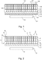
- An X-ray detector array such as shown in figure 1 has been provided e. g. for computer tomography.
- the X-ray detector array 101 comprises a scintillator pack 102.
- a scintillator pack 102 a plurality of scintillator pixels 103 is arranged in an array.
- Each scintillator pixel 103 comprises scintillator crystals 105, 107 which may convert penetrating X-rays into scintillation radiation, possibly in the visible spectral range.
- Each of the scintillators in each layer is associated with a photo-diode.
- a spectral x-ray image is constructed by processing and comparing the data output from these two photodiode array layers.
- a more extensive description of this scintillator arrangement is given in US7,968,853 B2 and US 2010/0220833 co-owned by the assignee of the present application.
- a scintillation radiation detector 109 is arranged adjacent to each of the scintillator pixels 103 at a side surface thereof.
- the scintillation radiation detector 109 may be provided as a vertical photodiode. Except for the side surface which is facing the scintillation radiation detector 109, all surfaces of the scintillator crystals are covered by a layer 111 of reflective paint which is highly reflective to scintillation radiation and which may reflect the scintillation radiation generated in the scintillator crystals towards an associated scintillation radiation detector surface.
- Each of the scintillator radiation detectors 109 is connected to a substrate 117 with an electrical joint 115 at a lower edge thereof. At a surface of the substrate 117 opposite to the surface directed to the scintillator pack 102, electronic circuits 118 are arranged. Furthermore, an optionally flexible input/output cable 121 is provided for electrically contacting the electronic circuit 118.
- the electronic circuit 118 may serve for amplification, digitization and/or multiplexing and is arranged below the substrate 117.
- the electronic circuit 118 may comprise an analog section dedicated, for example, to the amplification of fast changing currents in the pico-ampere range, it may be specifically this section which needs to be protected from direct X-ray radiation as such X-ray radiation may give rise to direct conversion and thereby to spurious signals.
- extended exposure may lead to damage, for example in the semiconductor material used for an integrated circuitry implementing the analog section and may thereby enhance leakage currents.
- a plate 120 made of tungsten or any other suitable material of high atomic number Z is placed between the substrate 117 and the electronic circuit 118.
- the electronic circuit 118 is mounted with its backside on the plate 120 and interconnections may be realized through wire bonding.
- Figure 2 shows an embodiment of an X-ray detector array 1 according to the present invention.
- a scintillator pack 2 comprises a plurality of scintillator pixels 3 each comprising scintillators 5, 7. Each of the scintillators 5, 7 is enclosed by a layer 11 of reflective paint in order to reflect scintillation radiation generated within the respective scintillator pixel 3 towards a side surface thereof. At this side surface, a vertical photo diode serves as a scintillation radiation detector 9. Each scintillation radiation detector 9 is connected via an electrical joint 15 to an interposer 17. At an opposite side of the interposer 17, ASICs are arranged for providing an electronic circuit 19. The ASICs are mounted in flip chip technology and are connected to an input/output cable 21.
- a top surface 27 of the scintillator pixels 3 is directed towards an X-ray source. X-rays may enter the scintillators 5, 7 and may be at least partly absorbed to generate scintillation radiation therein. Side surfaces 29 of the scintillator pixels 3 are covered with the layer 11 of reflective paint or by an associated scintillation radiation detector 9.
- a volume between the scintillator crystals 7 and the interposer 17 is filled with a highly X-ray absorbing material thereby forming an X-ray absorbing layer 13.
- This X-ray absorbing layer 13 comprises a high volume percentage of highly X-ray absorbing material having a high atomic number of more than 50. Due to this highly X-ray absorbing material, the layer 13 may serve as an X-ray protection barrier for the underlying electronic circuit 19. Substantially no X-rays transmitted through the scintillator pixels 3 may be further transmitted through the layer 13 due to its highly X-ray absorbing characteristics.
- the layer 13 may not only act as an X-ray barrier but may also serve for mechanical stabilization of the photodiodes forming the scintillation radiation detectors 9 on top of the interposer 17.
- a filler material used for the layer 13 may be, for example, Bismuth oxide (Bi 2 O 3 ).
- the high atomic number of Bismuth provides for good X-ray absorption properties of such filler material. It has been observed that an X-ray absorbing layer 13 comprising e.g. a high content of Bismuth oxide and having a thickness of 1 mm may show similar X-ray absorption properties as a Tungsten plate of 0.25 mm.
- Bismuth oxide is environmentally acceptable, non-poisonous and is a low cost material.
- the filler material is sufficiently electrically insulating such that e. g. spurious electrical shorts between the electrical joints 15 may be prevented.
- the photodiodes of the scintillation radiation detectors 9 may provide photo currents in the range of pico-ampere, such electrical insulation may be crucial. An electrical resistance of more than hundred Mega-Ohm (> 100 M ⁇ ) between neighbouring electrical joints may have to be achieved.
- Bismuth oxide as a filler material
- other filler materials including high Z number elements such as Lead oxide (Pb x O y ), Tantalum oxide (Ta 2 O 5 ), Uranium oxide (UO 2 ), Lutetium oxide (Lu 2 O 3 ), Gadolinium oxide (Gd 2 O 3 ) or other suitable oxides may be used.
- Tungsten metal particles coated with an isolating layer to maintain electrical insulation may be used in the X-ray absorbing layer 13.
- the filler material may, but does not necessarily have to, provide for high reflectivity to scintillation radiation.
- Bismuth oxide shows some absorption in the visible spectrum and has a yellowish appearance.
- such absorption does not matter as the filling material in the layer 13 does not have to serve for reflecting scintillation radiation as this effect is obtained by the layer 11 of reflective paint.
- the filler material for the layer 13 may include particles of highly X-ray absorbing material such as Bismuth oxide, such particles being integrated into a resin matrix.
- a filling degree is preferably as high as possible, but for practical reasons may be about 50% by volume or 90% by weight. At such formulation, a viscosity may still be low enough such that the particle resin mixture can be used for a filling process for filling spaces underneath the scintillator pixels 3 in order to generate the X-ray absorbing layer 13.
- a powder comprising Bismuth oxide particles of an average size of 10 micrometers maybe mixed with low-viscous epoxy adhesives.
- an effective dispersant is required to disperse the Bismuth oxide particles in the filler material.
- Maximum particle content may further be influenced by particle properties such as size, size distribution and shape.
- the properties of the filler material, particularly its viscosity and its content of Bismuth oxide particles may be adapted such that, on the one hand, the filler material may be easily introduced into the spaces underneath the scintillator pixels 3 in order to generate the X-ray absorbing layer 13 and, on the other hand, provide for sufficient X-ray absorption by such layer 13.
- X-ray absorbing particles i. e. Bismuth oxide particles
- such high content may result in high viscosity. Accordingly, the content of X-ray absorbing particles within the resin matrix of the filler material will have to be optimized.
Landscapes
- Health & Medical Sciences (AREA)
- Physics & Mathematics (AREA)
- Life Sciences & Earth Sciences (AREA)
- General Physics & Mathematics (AREA)
- High Energy & Nuclear Physics (AREA)
- Molecular Biology (AREA)
- Spectroscopy & Molecular Physics (AREA)
- Chemical & Material Sciences (AREA)
- Crystallography & Structural Chemistry (AREA)
- Radiology & Medical Imaging (AREA)
- Immunology (AREA)
- Theoretical Computer Science (AREA)
- Nuclear Medicine, Radiotherapy & Molecular Imaging (AREA)
- Analytical Chemistry (AREA)
- Biochemistry (AREA)
- General Health & Medical Sciences (AREA)
- Pulmonology (AREA)
- Pathology (AREA)
- Engineering & Computer Science (AREA)
- Measurement Of Radiation (AREA)
- Solid State Image Pick-Up Elements (AREA)
- Apparatus For Radiation Diagnosis (AREA)
- Conversion Of X-Rays Into Visible Images (AREA)
Applications Claiming Priority (2)
| Application Number | Priority Date | Filing Date | Title |
|---|---|---|---|
| US201161564407P | 2011-11-29 | 2011-11-29 | |
| PCT/IB2012/056665 WO2013080105A2 (en) | 2011-11-29 | 2012-11-23 | Scintillator pack comprising an x-ray absorbing encapsulation and x-ray detector array comprising such scintillator pack |
Publications (2)
| Publication Number | Publication Date |
|---|---|
| EP2751595A2 EP2751595A2 (en) | 2014-07-09 |
| EP2751595B1 true EP2751595B1 (en) | 2017-07-05 |
Family
ID=47603861
Family Applications (1)
| Application Number | Title | Priority Date | Filing Date |
|---|---|---|---|
| EP12818815.8A Active EP2751595B1 (en) | 2011-11-29 | 2012-11-23 | Scintillator pack comprising an x-ray absorbing encapsulation and x-ray detector array comprising such scintillator pack |
Country Status (8)
| Country | Link |
|---|---|
| US (1) | US9599728B2 (ru) |
| EP (1) | EP2751595B1 (ru) |
| JP (1) | JP6114300B2 (ru) |
| CN (1) | CN103959098B (ru) |
| BR (1) | BR112014012699A8 (ru) |
| IN (1) | IN2014CN03832A (ru) |
| RU (1) | RU2605520C2 (ru) |
| WO (1) | WO2013080105A2 (ru) |
Families Citing this family (9)
| Publication number | Priority date | Publication date | Assignee | Title |
|---|---|---|---|---|
| US9748300B2 (en) * | 2013-09-05 | 2017-08-29 | Koninklijke Philips N.V. | Radiation detector element |
| US9859316B2 (en) | 2014-06-06 | 2018-01-02 | Sharp Kabushiki Kaisha | Semiconductor device and method for manufacturing same |
| JP6739423B2 (ja) * | 2014-09-25 | 2020-08-12 | コーニンクレッカ フィリップス エヌ ヴェKoninklijke Philips N.V. | 光を発生させるセラミック材料 |
| JP6671839B2 (ja) * | 2014-10-07 | 2020-03-25 | キヤノン株式会社 | 放射線撮像装置及び撮像システム |
| EP3353576B1 (en) * | 2015-09-24 | 2020-07-01 | Prismatic Sensors AB | Modular x-ray detector |
| CN109690351B (zh) | 2016-09-23 | 2022-12-09 | 深圳帧观德芯科技有限公司 | 半导体x射线检测器的封装 |
| EP3399344B1 (en) * | 2017-05-03 | 2021-06-30 | ams International AG | Semiconductor device for indirect detection of electromagnetic radiation and method of production |
| CN109709594B (zh) * | 2018-12-18 | 2020-12-11 | 北京纳米维景科技有限公司 | 闪烁屏封装结构制造方法、闪烁屏封装结构及影像探测器 |
| CN111697109A (zh) * | 2020-07-09 | 2020-09-22 | 上海大学 | 一种柔性x射线探测器的制备方法及系统 |
Citations (3)
| Publication number | Priority date | Publication date | Assignee | Title |
|---|---|---|---|---|
| EP1298676A1 (en) * | 2000-06-20 | 2003-04-02 | Kanebo Limited | Radiation shielding material |
| US7405408B2 (en) * | 2003-12-09 | 2008-07-29 | Koninklijke Philips Electronics N.V. | Shielding for an x-ray detector |
| US20110198503A1 (en) * | 2010-01-22 | 2011-08-18 | DenCT Ltd | Methods and apparatus for multi-camera x-ray flat panel detector |
Family Cites Families (25)
| Publication number | Priority date | Publication date | Assignee | Title |
|---|---|---|---|---|
| JPH08122492A (ja) | 1994-10-19 | 1996-05-17 | Sumitomo Electric Ind Ltd | 放射線遮蔽材及びその製造方法 |
| DE69927241T2 (de) * | 1998-10-28 | 2006-06-29 | Philips Intellectual Property & Standards Gmbh | Verfahren zur herstellung eines geschichteten szintillationsdetektorelements |
| JP2001099941A (ja) | 1999-09-30 | 2001-04-13 | Hitachi Metals Ltd | 放射線遮蔽板、放射線検出器及び放射線遮蔽板の製造方法 |
| US6298113B1 (en) * | 2000-02-07 | 2001-10-02 | General Electric Company | Self aligning inter-scintillator reflector x-ray damage shield and method of manufacture |
| JP2003084066A (ja) | 2001-04-11 | 2003-03-19 | Nippon Kessho Kogaku Kk | 放射線検出器用部品、放射線検出器および放射線検出装置 |
| US6519313B2 (en) | 2001-05-30 | 2003-02-11 | General Electric Company | High-Z cast reflector compositions and method of manufacture |
| JP2003028986A (ja) | 2001-07-12 | 2003-01-29 | Mitsubishi Plastics Ind Ltd | 放射線遮蔽材料 |
| EP1543351A1 (en) * | 2002-09-18 | 2005-06-22 | Koninklijke Philips Electronics N.V. | X-ray detector with a plurality of detector units |
| WO2004027453A1 (en) * | 2002-09-18 | 2004-04-01 | Koninklijke Philips Electronics N.V. | Radiation detector |
| AU2003288652A1 (en) * | 2003-01-06 | 2004-07-29 | Koninklijke Philips Electronics N.V. | Radiation detector with shielded electronics for computed tomography |
| JP2004219318A (ja) * | 2003-01-16 | 2004-08-05 | Hamamatsu Photonics Kk | 放射線検出器 |
| CN101115344A (zh) | 2003-02-20 | 2008-01-30 | 因普有限公司 | 产生x射线的系统 |
| JP4500010B2 (ja) * | 2003-06-16 | 2010-07-14 | 株式会社日立メディコ | X線検出器及びこれを用いたx線ct装置 |
| RU2251124C1 (ru) * | 2003-10-14 | 2005-04-27 | ГОУ ВПО Уральский государственный технический университет-УПИ | СЦИНТИЛЛЯЦИОННЫЙ ДАТЧИК ЭЛЕКТРОННОГО И β-ИЗЛУЧЕНИЯ |
| US7166849B2 (en) * | 2004-08-09 | 2007-01-23 | General Electric Company | Scintillator array for use in a CT imaging system and method for making the scintillator array |
| EP1861733B1 (en) | 2005-03-16 | 2016-03-09 | Philips Intellectual Property & Standards GmbH | X-ray detector with in-pixel processing circuits |
| CN101166997A (zh) * | 2005-04-26 | 2008-04-23 | 皇家飞利浦电子股份有限公司 | 光谱ct的检测器阵列 |
| EP1876955B1 (en) | 2005-04-26 | 2016-11-23 | Koninklijke Philips N.V. | Double decker detector for spectral ct |
| CN101248371B (zh) | 2006-03-13 | 2012-02-22 | 日立金属株式会社 | 辐射探测器及其制造方法 |
| US7582879B2 (en) * | 2006-03-27 | 2009-09-01 | Analogic Corporation | Modular x-ray measurement system |
| KR20080106453A (ko) * | 2006-03-30 | 2008-12-05 | 코닌클리케 필립스 일렉트로닉스 엔.브이. | 방사선 디텍터 어레이 |
| US20080068815A1 (en) * | 2006-09-18 | 2008-03-20 | Oliver Richard Astley | Interface Assembly And Method for Integrating A Data Acquisition System on a Sensor Array |
| CN101903801B (zh) * | 2007-12-21 | 2014-01-29 | 皇家飞利浦电子股份有限公司 | 具有复合树脂中的闪烁体的辐射敏感探测器 |
| JP2010096616A (ja) | 2008-10-16 | 2010-04-30 | Fujifilm Corp | 放射線画像検出器 |
| US8373132B2 (en) * | 2009-02-06 | 2013-02-12 | Koninklijke Philips Electronics N. V. | Radiation detector with a stack of scintillator elements and photodiode arrays |
-
2012
- 2012-11-23 JP JP2014542978A patent/JP6114300B2/ja active Active
- 2012-11-23 IN IN3832CHN2014 patent/IN2014CN03832A/en unknown
- 2012-11-23 EP EP12818815.8A patent/EP2751595B1/en active Active
- 2012-11-23 RU RU2014126371/28A patent/RU2605520C2/ru active
- 2012-11-23 US US14/358,058 patent/US9599728B2/en active Active
- 2012-11-23 BR BR112014012699A patent/BR112014012699A8/pt not_active Application Discontinuation
- 2012-11-23 WO PCT/IB2012/056665 patent/WO2013080105A2/en active Application Filing
- 2012-11-23 CN CN201280058399.8A patent/CN103959098B/zh active Active
Patent Citations (3)
| Publication number | Priority date | Publication date | Assignee | Title |
|---|---|---|---|---|
| EP1298676A1 (en) * | 2000-06-20 | 2003-04-02 | Kanebo Limited | Radiation shielding material |
| US7405408B2 (en) * | 2003-12-09 | 2008-07-29 | Koninklijke Philips Electronics N.V. | Shielding for an x-ray detector |
| US20110198503A1 (en) * | 2010-01-22 | 2011-08-18 | DenCT Ltd | Methods and apparatus for multi-camera x-ray flat panel detector |
Also Published As
| Publication number | Publication date |
|---|---|
| JP6114300B2 (ja) | 2017-04-12 |
| IN2014CN03832A (ru) | 2015-07-03 |
| EP2751595A2 (en) | 2014-07-09 |
| CN103959098B (zh) | 2017-04-26 |
| WO2013080105A3 (en) | 2013-12-27 |
| US9599728B2 (en) | 2017-03-21 |
| US20140321609A1 (en) | 2014-10-30 |
| RU2605520C2 (ru) | 2016-12-20 |
| CN103959098A (zh) | 2014-07-30 |
| RU2014126371A (ru) | 2016-01-27 |
| BR112014012699A8 (pt) | 2017-06-20 |
| BR112014012699A2 (pt) | 2017-06-13 |
| JP2015503096A (ja) | 2015-01-29 |
| WO2013080105A2 (en) | 2013-06-06 |
Similar Documents
| Publication | Publication Date | Title |
|---|---|---|
| EP2751595B1 (en) | Scintillator pack comprising an x-ray absorbing encapsulation and x-ray detector array comprising such scintillator pack | |
| US9012857B2 (en) | Multi-layer horizontal computed tomography (CT) detector array with at least one thin photosensor array layer disposed between at least two scintillator array layers | |
| EP2671097B1 (en) | Single or multi-energy vertical radiation sensitive detectors | |
| KR102547798B1 (ko) | 방사선 검출기 및 이를 채용한 방사선 촬영 장치 | |
| JP5587788B2 (ja) | 複合樹脂におけるシンチレータを備えた放射線感受性検出器 | |
| US11275187B2 (en) | Detector array for a radiation system, and related system | |
| US11041966B2 (en) | Radiation detector scintillator with an integral through-hole interconnect | |
| US20130153775A1 (en) | Radiation detection apparatus | |
| JP2014510902A5 (ru) | ||
| KR20110013208A (ko) | 프로젝션 방사선 이미징 장치, 방사선 이미징 장치 제조 방법 및 방사선 이미징 패널 | |
| KR102154133B1 (ko) | 타일형 x-선 이미저 패널 및 그 제조 방법 | |
| US7211801B2 (en) | Radiation detector | |
| US9337233B1 (en) | Photodiode array for imaging applications | |
| JP4178402B2 (ja) | 放射線検出器 | |
| JP6548565B2 (ja) | シンチレータパネル、及び、放射線検出器 | |
| JP2004151007A (ja) | 放射線検出器 | |
| CN115530861A (zh) | 辐射检测器模块和成像系统 | |
| KR102604256B1 (ko) | 하이브리드 섬광체 기반 엑스선 디텍터 | |
| GB2311896A (en) | Detectors for high energy radiation |
Legal Events
| Date | Code | Title | Description |
|---|---|---|---|
| PUAI | Public reference made under article 153(3) epc to a published international application that has entered the european phase |
Free format text: ORIGINAL CODE: 0009012 |
|
| 17P | Request for examination filed |
Effective date: 20140331 |
|
| AK | Designated contracting states |
Kind code of ref document: A2 Designated state(s): AL AT BE BG CH CY CZ DE DK EE ES FI FR GB GR HR HU IE IS IT LI LT LU LV MC MK MT NL NO PL PT RO RS SE SI SK SM TR |
|
| DAX | Request for extension of the european patent (deleted) | ||
| 17Q | First examination report despatched |
Effective date: 20150330 |
|
| GRAP | Despatch of communication of intention to grant a patent |
Free format text: ORIGINAL CODE: EPIDOSNIGR1 |
|
| INTG | Intention to grant announced |
Effective date: 20170117 |
|
| GRAS | Grant fee paid |
Free format text: ORIGINAL CODE: EPIDOSNIGR3 |
|
| GRAA | (expected) grant |
Free format text: ORIGINAL CODE: 0009210 |
|
| AK | Designated contracting states |
Kind code of ref document: B1 Designated state(s): AL AT BE BG CH CY CZ DE DK EE ES FI FR GB GR HR HU IE IS IT LI LT LU LV MC MK MT NL NO PL PT RO RS SE SI SK SM TR |
|
| REG | Reference to a national code |
Ref country code: GB Ref legal event code: FG4D |
|
| REG | Reference to a national code |
Ref country code: CH Ref legal event code: EP |
|
| REG | Reference to a national code |
Ref country code: AT Ref legal event code: REF Ref document number: 906975 Country of ref document: AT Kind code of ref document: T Effective date: 20170715 |
|
| REG | Reference to a national code |
Ref country code: IE Ref legal event code: FG4D |
|
| REG | Reference to a national code |
Ref country code: DE Ref legal event code: R096 Ref document number: 602012034255 Country of ref document: DE |
|
| REG | Reference to a national code |
Ref country code: DE Ref legal event code: R084 Ref document number: 602012034255 Country of ref document: DE |
|
| REG | Reference to a national code |
Ref country code: DE Ref legal event code: R081 Ref document number: 602012034255 Country of ref document: DE Owner name: KONINKLIJKE PHILIPS N.V., NL Free format text: FORMER OWNER: KONINKLIJKE PHILIPS ELECTRONICS B.V., EINDHOVEN, NL Ref country code: DE Ref legal event code: R081 Ref document number: 602012034255 Country of ref document: DE Owner name: KONINKLIJKE PHILIPS ELECTRONICS N.V., NL Free format text: FORMER OWNER: KONINKLIJKE PHILIPS ELECTRONICS B.V., EINDHOVEN, NL |
|
| REG | Reference to a national code |
Ref country code: DE Ref legal event code: R082 Ref document number: 602012034255 Country of ref document: DE |
|
| REG | Reference to a national code |
Ref country code: NL Ref legal event code: MP Effective date: 20170705 |
|
| REG | Reference to a national code |
Ref country code: AT Ref legal event code: MK05 Ref document number: 906975 Country of ref document: AT Kind code of ref document: T Effective date: 20170705 |
|
| REG | Reference to a national code |
Ref country code: LT Ref legal event code: MG4D Ref country code: FR Ref legal event code: PLFP Year of fee payment: 6 |
|
| PG25 | Lapsed in a contracting state [announced via postgrant information from national office to epo] |
Ref country code: SE Free format text: LAPSE BECAUSE OF FAILURE TO SUBMIT A TRANSLATION OF THE DESCRIPTION OR TO PAY THE FEE WITHIN THE PRESCRIBED TIME-LIMIT Effective date: 20170705 Ref country code: AT Free format text: LAPSE BECAUSE OF FAILURE TO SUBMIT A TRANSLATION OF THE DESCRIPTION OR TO PAY THE FEE WITHIN THE PRESCRIBED TIME-LIMIT Effective date: 20170705 Ref country code: LT Free format text: LAPSE BECAUSE OF FAILURE TO SUBMIT A TRANSLATION OF THE DESCRIPTION OR TO PAY THE FEE WITHIN THE PRESCRIBED TIME-LIMIT Effective date: 20170705 Ref country code: NL Free format text: LAPSE BECAUSE OF FAILURE TO SUBMIT A TRANSLATION OF THE DESCRIPTION OR TO PAY THE FEE WITHIN THE PRESCRIBED TIME-LIMIT Effective date: 20170705 Ref country code: FI Free format text: LAPSE BECAUSE OF FAILURE TO SUBMIT A TRANSLATION OF THE DESCRIPTION OR TO PAY THE FEE WITHIN THE PRESCRIBED TIME-LIMIT Effective date: 20170705 Ref country code: HR Free format text: LAPSE BECAUSE OF FAILURE TO SUBMIT A TRANSLATION OF THE DESCRIPTION OR TO PAY THE FEE WITHIN THE PRESCRIBED TIME-LIMIT Effective date: 20170705 Ref country code: NO Free format text: LAPSE BECAUSE OF FAILURE TO SUBMIT A TRANSLATION OF THE DESCRIPTION OR TO PAY THE FEE WITHIN THE PRESCRIBED TIME-LIMIT Effective date: 20171005 |
|
| PG25 | Lapsed in a contracting state [announced via postgrant information from national office to epo] |
Ref country code: IS Free format text: LAPSE BECAUSE OF FAILURE TO SUBMIT A TRANSLATION OF THE DESCRIPTION OR TO PAY THE FEE WITHIN THE PRESCRIBED TIME-LIMIT Effective date: 20171105 Ref country code: LV Free format text: LAPSE BECAUSE OF FAILURE TO SUBMIT A TRANSLATION OF THE DESCRIPTION OR TO PAY THE FEE WITHIN THE PRESCRIBED TIME-LIMIT Effective date: 20170705 Ref country code: BG Free format text: LAPSE BECAUSE OF FAILURE TO SUBMIT A TRANSLATION OF THE DESCRIPTION OR TO PAY THE FEE WITHIN THE PRESCRIBED TIME-LIMIT Effective date: 20171005 Ref country code: PL Free format text: LAPSE BECAUSE OF FAILURE TO SUBMIT A TRANSLATION OF THE DESCRIPTION OR TO PAY THE FEE WITHIN THE PRESCRIBED TIME-LIMIT Effective date: 20170705 Ref country code: RS Free format text: LAPSE BECAUSE OF FAILURE TO SUBMIT A TRANSLATION OF THE DESCRIPTION OR TO PAY THE FEE WITHIN THE PRESCRIBED TIME-LIMIT Effective date: 20170705 Ref country code: ES Free format text: LAPSE BECAUSE OF FAILURE TO SUBMIT A TRANSLATION OF THE DESCRIPTION OR TO PAY THE FEE WITHIN THE PRESCRIBED TIME-LIMIT Effective date: 20170705 Ref country code: GR Free format text: LAPSE BECAUSE OF FAILURE TO SUBMIT A TRANSLATION OF THE DESCRIPTION OR TO PAY THE FEE WITHIN THE PRESCRIBED TIME-LIMIT Effective date: 20171006 |
|
| REG | Reference to a national code |
Ref country code: DE Ref legal event code: R097 Ref document number: 602012034255 Country of ref document: DE |
|
| PG25 | Lapsed in a contracting state [announced via postgrant information from national office to epo] |
Ref country code: DK Free format text: LAPSE BECAUSE OF FAILURE TO SUBMIT A TRANSLATION OF THE DESCRIPTION OR TO PAY THE FEE WITHIN THE PRESCRIBED TIME-LIMIT Effective date: 20170705 Ref country code: CZ Free format text: LAPSE BECAUSE OF FAILURE TO SUBMIT A TRANSLATION OF THE DESCRIPTION OR TO PAY THE FEE WITHIN THE PRESCRIBED TIME-LIMIT Effective date: 20170705 Ref country code: RO Free format text: LAPSE BECAUSE OF FAILURE TO SUBMIT A TRANSLATION OF THE DESCRIPTION OR TO PAY THE FEE WITHIN THE PRESCRIBED TIME-LIMIT Effective date: 20170705 |
|
| PLBE | No opposition filed within time limit |
Free format text: ORIGINAL CODE: 0009261 |
|
| STAA | Information on the status of an ep patent application or granted ep patent |
Free format text: STATUS: NO OPPOSITION FILED WITHIN TIME LIMIT |
|
| PG25 | Lapsed in a contracting state [announced via postgrant information from national office to epo] |
Ref country code: SM Free format text: LAPSE BECAUSE OF FAILURE TO SUBMIT A TRANSLATION OF THE DESCRIPTION OR TO PAY THE FEE WITHIN THE PRESCRIBED TIME-LIMIT Effective date: 20170705 Ref country code: SK Free format text: LAPSE BECAUSE OF FAILURE TO SUBMIT A TRANSLATION OF THE DESCRIPTION OR TO PAY THE FEE WITHIN THE PRESCRIBED TIME-LIMIT Effective date: 20170705 Ref country code: IT Free format text: LAPSE BECAUSE OF FAILURE TO SUBMIT A TRANSLATION OF THE DESCRIPTION OR TO PAY THE FEE WITHIN THE PRESCRIBED TIME-LIMIT Effective date: 20170705 Ref country code: EE Free format text: LAPSE BECAUSE OF FAILURE TO SUBMIT A TRANSLATION OF THE DESCRIPTION OR TO PAY THE FEE WITHIN THE PRESCRIBED TIME-LIMIT Effective date: 20170705 |
|
| 26N | No opposition filed |
Effective date: 20180406 |
|
| PG25 | Lapsed in a contracting state [announced via postgrant information from national office to epo] |
Ref country code: MC Free format text: LAPSE BECAUSE OF FAILURE TO SUBMIT A TRANSLATION OF THE DESCRIPTION OR TO PAY THE FEE WITHIN THE PRESCRIBED TIME-LIMIT Effective date: 20170705 |
|
| GBPC | Gb: european patent ceased through non-payment of renewal fee |
Effective date: 20171123 |
|
| PG25 | Lapsed in a contracting state [announced via postgrant information from national office to epo] |
Ref country code: CH Free format text: LAPSE BECAUSE OF NON-PAYMENT OF DUE FEES Effective date: 20171130 Ref country code: LI Free format text: LAPSE BECAUSE OF NON-PAYMENT OF DUE FEES Effective date: 20171130 |
|
| PG25 | Lapsed in a contracting state [announced via postgrant information from national office to epo] |
Ref country code: LU Free format text: LAPSE BECAUSE OF NON-PAYMENT OF DUE FEES Effective date: 20171123 Ref country code: SI Free format text: LAPSE BECAUSE OF FAILURE TO SUBMIT A TRANSLATION OF THE DESCRIPTION OR TO PAY THE FEE WITHIN THE PRESCRIBED TIME-LIMIT Effective date: 20170705 |
|
| REG | Reference to a national code |
Ref country code: BE Ref legal event code: MM Effective date: 20171130 |
|
| REG | Reference to a national code |
Ref country code: IE Ref legal event code: MM4A |
|
| PG25 | Lapsed in a contracting state [announced via postgrant information from national office to epo] |
Ref country code: MT Free format text: LAPSE BECAUSE OF NON-PAYMENT OF DUE FEES Effective date: 20171123 |
|
| PG25 | Lapsed in a contracting state [announced via postgrant information from national office to epo] |
Ref country code: IE Free format text: LAPSE BECAUSE OF NON-PAYMENT OF DUE FEES Effective date: 20171123 |
|
| PG25 | Lapsed in a contracting state [announced via postgrant information from national office to epo] |
Ref country code: GB Free format text: LAPSE BECAUSE OF NON-PAYMENT OF DUE FEES Effective date: 20171123 Ref country code: BE Free format text: LAPSE BECAUSE OF NON-PAYMENT OF DUE FEES Effective date: 20171130 |
|
| PG25 | Lapsed in a contracting state [announced via postgrant information from national office to epo] |
Ref country code: HU Free format text: LAPSE BECAUSE OF FAILURE TO SUBMIT A TRANSLATION OF THE DESCRIPTION OR TO PAY THE FEE WITHIN THE PRESCRIBED TIME-LIMIT; INVALID AB INITIO Effective date: 20121123 |
|
| PG25 | Lapsed in a contracting state [announced via postgrant information from national office to epo] |
Ref country code: CY Free format text: LAPSE BECAUSE OF NON-PAYMENT OF DUE FEES Effective date: 20170705 |
|
| PG25 | Lapsed in a contracting state [announced via postgrant information from national office to epo] |
Ref country code: MK Free format text: LAPSE BECAUSE OF FAILURE TO SUBMIT A TRANSLATION OF THE DESCRIPTION OR TO PAY THE FEE WITHIN THE PRESCRIBED TIME-LIMIT Effective date: 20170705 |
|
| PG25 | Lapsed in a contracting state [announced via postgrant information from national office to epo] |
Ref country code: TR Free format text: LAPSE BECAUSE OF FAILURE TO SUBMIT A TRANSLATION OF THE DESCRIPTION OR TO PAY THE FEE WITHIN THE PRESCRIBED TIME-LIMIT Effective date: 20170705 |
|
| PG25 | Lapsed in a contracting state [announced via postgrant information from national office to epo] |
Ref country code: PT Free format text: LAPSE BECAUSE OF FAILURE TO SUBMIT A TRANSLATION OF THE DESCRIPTION OR TO PAY THE FEE WITHIN THE PRESCRIBED TIME-LIMIT Effective date: 20170705 |
|
| PG25 | Lapsed in a contracting state [announced via postgrant information from national office to epo] |
Ref country code: AL Free format text: LAPSE BECAUSE OF FAILURE TO SUBMIT A TRANSLATION OF THE DESCRIPTION OR TO PAY THE FEE WITHIN THE PRESCRIBED TIME-LIMIT Effective date: 20170705 |
|
| REG | Reference to a national code |
Ref country code: DE Ref legal event code: R081 Ref document number: 602012034255 Country of ref document: DE Owner name: KONINKLIJKE PHILIPS N.V., NL Free format text: FORMER OWNER: KONINKLIJKE PHILIPS ELECTRONICS N.V., EINDHOVEN, NL |
|
| PGFP | Annual fee paid to national office [announced via postgrant information from national office to epo] |
Ref country code: FR Payment date: 20231123 Year of fee payment: 12 Ref country code: DE Payment date: 20231127 Year of fee payment: 12 |