EP2749374A1 - Solder piece, chip solder, and method for manufacturing solder piece - Google Patents
Solder piece, chip solder, and method for manufacturing solder piece Download PDFInfo
- Publication number
- EP2749374A1 EP2749374A1 EP11808554.7A EP11808554A EP2749374A1 EP 2749374 A1 EP2749374 A1 EP 2749374A1 EP 11808554 A EP11808554 A EP 11808554A EP 2749374 A1 EP2749374 A1 EP 2749374A1
- Authority
- EP
- European Patent Office
- Prior art keywords
- solder
- solder piece
- sucked
- shear droop
- opposite
- Prior art date
- Legal status (The legal status is an assumption and is not a legal conclusion. Google has not performed a legal analysis and makes no representation as to the accuracy of the status listed.)
- Granted
Links
Images



Classifications
-
- B—PERFORMING OPERATIONS; TRANSPORTING
- B23—MACHINE TOOLS; METAL-WORKING NOT OTHERWISE PROVIDED FOR
- B23K—SOLDERING OR UNSOLDERING; WELDING; CLADDING OR PLATING BY SOLDERING OR WELDING; CUTTING BY APPLYING HEAT LOCALLY, e.g. FLAME CUTTING; WORKING BY LASER BEAM
- B23K35/00—Rods, electrodes, materials, or media, for use in soldering, welding, or cutting
- B23K35/02—Rods, electrodes, materials, or media, for use in soldering, welding, or cutting characterised by mechanical features, e.g. shape
- B23K35/0222—Rods, electrodes, materials, or media, for use in soldering, welding, or cutting characterised by mechanical features, e.g. shape for use in soldering or brazing
-
- B—PERFORMING OPERATIONS; TRANSPORTING
- B23—MACHINE TOOLS; METAL-WORKING NOT OTHERWISE PROVIDED FOR
- B23K—SOLDERING OR UNSOLDERING; WELDING; CLADDING OR PLATING BY SOLDERING OR WELDING; CUTTING BY APPLYING HEAT LOCALLY, e.g. FLAME CUTTING; WORKING BY LASER BEAM
- B23K1/00—Soldering, e.g. brazing, or unsoldering
- B23K1/0008—Soldering, e.g. brazing, or unsoldering specially adapted for particular articles or work
- B23K1/0016—Soldering of electronic components
-
- B—PERFORMING OPERATIONS; TRANSPORTING
- B23—MACHINE TOOLS; METAL-WORKING NOT OTHERWISE PROVIDED FOR
- B23K—SOLDERING OR UNSOLDERING; WELDING; CLADDING OR PLATING BY SOLDERING OR WELDING; CUTTING BY APPLYING HEAT LOCALLY, e.g. FLAME CUTTING; WORKING BY LASER BEAM
- B23K1/00—Soldering, e.g. brazing, or unsoldering
- B23K1/008—Soldering within a furnace
-
- B—PERFORMING OPERATIONS; TRANSPORTING
- B23—MACHINE TOOLS; METAL-WORKING NOT OTHERWISE PROVIDED FOR
- B23K—SOLDERING OR UNSOLDERING; WELDING; CLADDING OR PLATING BY SOLDERING OR WELDING; CUTTING BY APPLYING HEAT LOCALLY, e.g. FLAME CUTTING; WORKING BY LASER BEAM
- B23K3/00—Tools, devices or special appurtenances for soldering, e.g. brazing, or unsoldering, not specially adapted for particular methods
- B23K3/06—Solder feeding devices; Solder melting pans
- B23K3/0607—Solder feeding devices
- B23K3/0623—Solder feeding devices for shaped solder piece feeding, e.g. preforms, bumps, balls, pellets, droplets
-
- B—PERFORMING OPERATIONS; TRANSPORTING
- B23—MACHINE TOOLS; METAL-WORKING NOT OTHERWISE PROVIDED FOR
- B23K—SOLDERING OR UNSOLDERING; WELDING; CLADDING OR PLATING BY SOLDERING OR WELDING; CUTTING BY APPLYING HEAT LOCALLY, e.g. FLAME CUTTING; WORKING BY LASER BEAM
- B23K35/00—Rods, electrodes, materials, or media, for use in soldering, welding, or cutting
- B23K35/02—Rods, electrodes, materials, or media, for use in soldering, welding, or cutting characterised by mechanical features, e.g. shape
-
- B—PERFORMING OPERATIONS; TRANSPORTING
- B23—MACHINE TOOLS; METAL-WORKING NOT OTHERWISE PROVIDED FOR
- B23K—SOLDERING OR UNSOLDERING; WELDING; CLADDING OR PLATING BY SOLDERING OR WELDING; CUTTING BY APPLYING HEAT LOCALLY, e.g. FLAME CUTTING; WORKING BY LASER BEAM
- B23K35/00—Rods, electrodes, materials, or media, for use in soldering, welding, or cutting
- B23K35/22—Rods, electrodes, materials, or media, for use in soldering, welding, or cutting characterised by the composition or nature of the material
- B23K35/24—Selection of soldering or welding materials proper
- B23K35/26—Selection of soldering or welding materials proper with the principal constituent melting at less than 400°C
-
- B—PERFORMING OPERATIONS; TRANSPORTING
- B23—MACHINE TOOLS; METAL-WORKING NOT OTHERWISE PROVIDED FOR
- B23K—SOLDERING OR UNSOLDERING; WELDING; CLADDING OR PLATING BY SOLDERING OR WELDING; CUTTING BY APPLYING HEAT LOCALLY, e.g. FLAME CUTTING; WORKING BY LASER BEAM
- B23K35/00—Rods, electrodes, materials, or media, for use in soldering, welding, or cutting
- B23K35/22—Rods, electrodes, materials, or media, for use in soldering, welding, or cutting characterised by the composition or nature of the material
- B23K35/24—Selection of soldering or welding materials proper
- B23K35/26—Selection of soldering or welding materials proper with the principal constituent melting at less than 400°C
- B23K35/262—Sn as the principal constituent
-
- B—PERFORMING OPERATIONS; TRANSPORTING
- B23—MACHINE TOOLS; METAL-WORKING NOT OTHERWISE PROVIDED FOR
- B23K—SOLDERING OR UNSOLDERING; WELDING; CLADDING OR PLATING BY SOLDERING OR WELDING; CUTTING BY APPLYING HEAT LOCALLY, e.g. FLAME CUTTING; WORKING BY LASER BEAM
- B23K35/00—Rods, electrodes, materials, or media, for use in soldering, welding, or cutting
- B23K35/22—Rods, electrodes, materials, or media, for use in soldering, welding, or cutting characterised by the composition or nature of the material
- B23K35/24—Selection of soldering or welding materials proper
- B23K35/28—Selection of soldering or welding materials proper with the principal constituent melting at less than 950°C
- B23K35/286—Al as the principal constituent
-
- B—PERFORMING OPERATIONS; TRANSPORTING
- B23—MACHINE TOOLS; METAL-WORKING NOT OTHERWISE PROVIDED FOR
- B23K—SOLDERING OR UNSOLDERING; WELDING; CLADDING OR PLATING BY SOLDERING OR WELDING; CUTTING BY APPLYING HEAT LOCALLY, e.g. FLAME CUTTING; WORKING BY LASER BEAM
- B23K35/00—Rods, electrodes, materials, or media, for use in soldering, welding, or cutting
- B23K35/22—Rods, electrodes, materials, or media, for use in soldering, welding, or cutting characterised by the composition or nature of the material
- B23K35/24—Selection of soldering or welding materials proper
- B23K35/30—Selection of soldering or welding materials proper with the principal constituent melting at less than 1550°C
- B23K35/302—Cu as the principal constituent
-
- B—PERFORMING OPERATIONS; TRANSPORTING
- B23—MACHINE TOOLS; METAL-WORKING NOT OTHERWISE PROVIDED FOR
- B23K—SOLDERING OR UNSOLDERING; WELDING; CLADDING OR PLATING BY SOLDERING OR WELDING; CUTTING BY APPLYING HEAT LOCALLY, e.g. FLAME CUTTING; WORKING BY LASER BEAM
- B23K35/00—Rods, electrodes, materials, or media, for use in soldering, welding, or cutting
- B23K35/22—Rods, electrodes, materials, or media, for use in soldering, welding, or cutting characterised by the composition or nature of the material
- B23K35/24—Selection of soldering or welding materials proper
- B23K35/32—Selection of soldering or welding materials proper with the principal constituent melting at more than 1550°C
- B23K35/325—Ti as the principal constituent
-
- B—PERFORMING OPERATIONS; TRANSPORTING
- B23—MACHINE TOOLS; METAL-WORKING NOT OTHERWISE PROVIDED FOR
- B23K—SOLDERING OR UNSOLDERING; WELDING; CLADDING OR PLATING BY SOLDERING OR WELDING; CUTTING BY APPLYING HEAT LOCALLY, e.g. FLAME CUTTING; WORKING BY LASER BEAM
- B23K35/00—Rods, electrodes, materials, or media, for use in soldering, welding, or cutting
- B23K35/40—Making wire or rods for soldering or welding
-
- B—PERFORMING OPERATIONS; TRANSPORTING
- B26—HAND CUTTING TOOLS; CUTTING; SEVERING
- B26F—PERFORATING; PUNCHING; CUTTING-OUT; STAMPING-OUT; SEVERING BY MEANS OTHER THAN CUTTING
- B26F1/00—Perforating; Punching; Cutting-out; Stamping-out; Apparatus therefor
- B26F1/02—Perforating by punching, e.g. with relatively-reciprocating punch and bed
-
- H—ELECTRICITY
- H05—ELECTRIC TECHNIQUES NOT OTHERWISE PROVIDED FOR
- H05K—PRINTED CIRCUITS; CASINGS OR CONSTRUCTIONAL DETAILS OF ELECTRIC APPARATUS; MANUFACTURE OF ASSEMBLAGES OF ELECTRICAL COMPONENTS
- H05K3/00—Apparatus or processes for manufacturing printed circuits
- H05K3/30—Assembling printed circuits with electric components, e.g. with resistors
- H05K3/32—Assembling printed circuits with electric components, e.g. with resistors electrically connecting electric components or wires to printed circuits
- H05K3/34—Assembling printed circuits with electric components, e.g. with resistors electrically connecting electric components or wires to printed circuits by soldering
-
- H—ELECTRICITY
- H05—ELECTRIC TECHNIQUES NOT OTHERWISE PROVIDED FOR
- H05K—PRINTED CIRCUITS; CASINGS OR CONSTRUCTIONAL DETAILS OF ELECTRIC APPARATUS; MANUFACTURE OF ASSEMBLAGES OF ELECTRICAL COMPONENTS
- H05K3/00—Apparatus or processes for manufacturing printed circuits
- H05K3/30—Assembling printed circuits with electric components, e.g. with resistors
- H05K3/32—Assembling printed circuits with electric components, e.g. with resistors electrically connecting electric components or wires to printed circuits
- H05K3/34—Assembling printed circuits with electric components, e.g. with resistors electrically connecting electric components or wires to printed circuits by soldering
- H05K3/3465—Application of solder
- H05K3/3478—Application of solder preforms; Transferring prefabricated solder patterns
-
- B—PERFORMING OPERATIONS; TRANSPORTING
- B23—MACHINE TOOLS; METAL-WORKING NOT OTHERWISE PROVIDED FOR
- B23K—SOLDERING OR UNSOLDERING; WELDING; CLADDING OR PLATING BY SOLDERING OR WELDING; CUTTING BY APPLYING HEAT LOCALLY, e.g. FLAME CUTTING; WORKING BY LASER BEAM
- B23K2101/00—Articles made by soldering, welding or cutting
- B23K2101/36—Electric or electronic devices
- B23K2101/42—Printed circuits
-
- H—ELECTRICITY
- H05—ELECTRIC TECHNIQUES NOT OTHERWISE PROVIDED FOR
- H05K—PRINTED CIRCUITS; CASINGS OR CONSTRUCTIONAL DETAILS OF ELECTRIC APPARATUS; MANUFACTURE OF ASSEMBLAGES OF ELECTRICAL COMPONENTS
- H05K2201/00—Indexing scheme relating to printed circuits covered by H05K1/00
- H05K2201/10—Details of components or other objects attached to or integrated in a printed circuit board
- H05K2201/10613—Details of electrical connections of non-printed components, e.g. special leads
- H05K2201/10621—Components characterised by their electrical contacts
- H05K2201/10636—Leadless chip, e.g. chip capacitor or resistor
-
- H—ELECTRICITY
- H05—ELECTRIC TECHNIQUES NOT OTHERWISE PROVIDED FOR
- H05K—PRINTED CIRCUITS; CASINGS OR CONSTRUCTIONAL DETAILS OF ELECTRIC APPARATUS; MANUFACTURE OF ASSEMBLAGES OF ELECTRICAL COMPONENTS
- H05K2201/00—Indexing scheme relating to printed circuits covered by H05K1/00
- H05K2201/10—Details of components or other objects attached to or integrated in a printed circuit board
- H05K2201/10613—Details of electrical connections of non-printed components, e.g. special leads
- H05K2201/10954—Other details of electrical connections
- H05K2201/10992—Using different connection materials, e.g. different solders, for the same connection
-
- H—ELECTRICITY
- H05—ELECTRIC TECHNIQUES NOT OTHERWISE PROVIDED FOR
- H05K—PRINTED CIRCUITS; CASINGS OR CONSTRUCTIONAL DETAILS OF ELECTRIC APPARATUS; MANUFACTURE OF ASSEMBLAGES OF ELECTRICAL COMPONENTS
- H05K2203/00—Indexing scheme relating to apparatus or processes for manufacturing printed circuits covered by H05K3/00
- H05K2203/04—Soldering or other types of metallurgic bonding
- H05K2203/0415—Small preforms other than balls, e.g. discs, cylinders or pillars
-
- H—ELECTRICITY
- H05—ELECTRIC TECHNIQUES NOT OTHERWISE PROVIDED FOR
- H05K—PRINTED CIRCUITS; CASINGS OR CONSTRUCTIONAL DETAILS OF ELECTRIC APPARATUS; MANUFACTURE OF ASSEMBLAGES OF ELECTRICAL COMPONENTS
- H05K2203/00—Indexing scheme relating to apparatus or processes for manufacturing printed circuits covered by H05K3/00
- H05K2203/08—Treatments involving gases
- H05K2203/082—Suction, e.g. for holding solder balls or components
-
- H—ELECTRICITY
- H05—ELECTRIC TECHNIQUES NOT OTHERWISE PROVIDED FOR
- H05K—PRINTED CIRCUITS; CASINGS OR CONSTRUCTIONAL DETAILS OF ELECTRIC APPARATUS; MANUFACTURE OF ASSEMBLAGES OF ELECTRICAL COMPONENTS
- H05K3/00—Apparatus or processes for manufacturing printed circuits
- H05K3/30—Assembling printed circuits with electric components, e.g. with resistors
- H05K3/32—Assembling printed circuits with electric components, e.g. with resistors electrically connecting electric components or wires to printed circuits
- H05K3/34—Assembling printed circuits with electric components, e.g. with resistors electrically connecting electric components or wires to printed circuits by soldering
- H05K3/3465—Application of solder
- H05K3/3485—Application of solder paste, slurry or powder
-
- Y—GENERAL TAGGING OF NEW TECHNOLOGICAL DEVELOPMENTS; GENERAL TAGGING OF CROSS-SECTIONAL TECHNOLOGIES SPANNING OVER SEVERAL SECTIONS OF THE IPC; TECHNICAL SUBJECTS COVERED BY FORMER USPC CROSS-REFERENCE ART COLLECTIONS [XRACs] AND DIGESTS
- Y02—TECHNOLOGIES OR APPLICATIONS FOR MITIGATION OR ADAPTATION AGAINST CLIMATE CHANGE
- Y02P—CLIMATE CHANGE MITIGATION TECHNOLOGIES IN THE PRODUCTION OR PROCESSING OF GOODS
- Y02P70/00—Climate change mitigation technologies in the production process for final industrial or consumer products
- Y02P70/50—Manufacturing or production processes characterised by the final manufactured product
-
- Y—GENERAL TAGGING OF NEW TECHNOLOGICAL DEVELOPMENTS; GENERAL TAGGING OF CROSS-SECTIONAL TECHNOLOGIES SPANNING OVER SEVERAL SECTIONS OF THE IPC; TECHNICAL SUBJECTS COVERED BY FORMER USPC CROSS-REFERENCE ART COLLECTIONS [XRACs] AND DIGESTS
- Y10—TECHNICAL SUBJECTS COVERED BY FORMER USPC
- Y10T—TECHNICAL SUBJECTS COVERED BY FORMER US CLASSIFICATION
- Y10T83/00—Cutting
- Y10T83/04—Processes
- Y10T83/0448—With subsequent handling [i.e., of product]
-
- Y—GENERAL TAGGING OF NEW TECHNOLOGICAL DEVELOPMENTS; GENERAL TAGGING OF CROSS-SECTIONAL TECHNOLOGIES SPANNING OVER SEVERAL SECTIONS OF THE IPC; TECHNICAL SUBJECTS COVERED BY FORMER USPC CROSS-REFERENCE ART COLLECTIONS [XRACs] AND DIGESTS
- Y10—TECHNICAL SUBJECTS COVERED BY FORMER USPC
- Y10T—TECHNICAL SUBJECTS COVERED BY FORMER US CLASSIFICATION
- Y10T83/00—Cutting
- Y10T83/04—Processes
- Y10T83/0481—Puncturing
Definitions
- the present invention relates to a solder piece that is used in a soldering process of electronic components mounted on a land on a substrate, a chip solder receiving the solder piece and a method of fabricating the solder piece.
- soldering technology in which by applying a solder paste to the land formed on the substrate, mounting the electronic components on the solder-paste-applied land of the substrate and melting the solder paste, the soldering is carried out has been conventionally used.
- an amount of solder may be in short supply by only the solder paste applied to the land.
- Patent Document 1 Japanese Patent Application Publication No. H06-275944
- the solder piece is configured so as to become a desired shape by performing a punching process on a sheet member.
- the solder piece is fabricated by the punching process with a surface thereof including a curved surface, which is so called as "shear droop portion", being formed on a surface which is opposite to a surface pushed by a punch.
- solder piece thus fabricated is received in an opened concave portion formed in a long supply tape and then, a cover tape is sealed on it, which is then supplied.
- the solder piece received in the opened concave portion is sucked and maintained by a vacuum suction and is taken out of the supply tape after the cover tape has been removed, so that it is mounted on the substrate.
- the invention solves such a problem, and has an obj ect to provide a solder piece that prevents its surface on which the shear droop portion generated by the punching process is formed from becoming the sucked surface, a chip solder receiving the solder piece and a method of fabricating the solder piece.
- the invention relates to a solder piece that is configured so as to be a rectangular parallelepiped shape by a punching process wherein of four surfaces of the rectangular parallelepiped excluding from surfaces thereof a surface on which the shear droop portion generated by the punching process is formed and a surface that is opposite to the surface on which the shear droop portion is formed, any one surface of at least two opposite surfaces thereof is an sucked surface.
- the invention also relates to a chip solder which contains a solder piece that is configured so as to be a rectangular parallelepiped shape by a punching process and a supply tape in which an opened concave portion that receives the solder piece is formed, wherein of four surfaces the rectangular parallelepiped excluding from surfaces thereof a surface on which the shear droop portion generated by the punching process is formed and a surface that is opposite to the surface on which the shear droop portion is formed, any one surface of at least two opposite surfaces thereof is a sucked surface, and wherein the opened concave portion is configured so as to have a shape such that, of four surfaces of the rectangular parallelepiped excluding from the surfaces thereof the surface on which the shear droop portion is formed and the surface that is opposite to the surface on which the shear droop portion is formed, at least a surface which can be the sucked surface or a surface which is opposite to the surface that can be the sucked surface is exposed.
- the invention relates to a method of fabricating a solder piece that is configured so as to be a rectangular parallelepiped shape by a punching process wherein of four surfaces of the rectangular parallelepiped excluding from surfaces thereof a surface on which the shear droop portion generated by the punching process is formed and a surface that is opposite to the surface on which the shear droop portion is formed, any one surface of at least two opposite surfaces thereof is a sucked surface, the method comprising a step of punching a material with the four surfaces including a surface which can be the sucked surface being shared surfaces.
- the solder piece is configured so as to have a rectangular parallelepiped shape having six surfaces by a punching process.
- the solder piece is configured so that, of four surfaces of the rectangular parallelepiped excluding a surface on which the shear droop portion generated by the punching process is formed and a surface that is opposite to the surface on which the shear droop portion is formed, any one surface thereof is a sucked surface.
- the solder piece In the chip solder in which the solder piece is received in the supply tape, the solder piece is not received in the opened concave portion with the surface on which the shear droop portion is formed being exposed but the solder piece is received therein with the surface which can be the sucked surface being exposed from the opened concave portion.
- the invention it is possible to prevent the surface on which the shear droop portion generated by the punching process is formed from becoming a sucked surface of the solder piece. This enables the solder piece to be securely sucked, thereby allowing an occurrence of the failure of suction to be avoided and allowing to be also avoided the failure to supply the solder piece accompanying the failure of suction.
- FIG. 1 is a perspective view of the solder piece according to this embodiment for showing an example thereof.
- FIG. 2 is a side view of the solder piece according to this embodiment for showing the example thereof.
- the solder piece 1A has a rectangular parallelepiped shape composed of six surfaces and is fabricated by a punching process in which a tape like sheet member is punched out.
- the solder piece 1A is provided with four surfaces or two surfaces which can be an sucked surface on the occasion of handling, in this embodiment, four surfaces of a first surface 11, a second surface 12, a third surface 13 and a fourth surface 14, a fifth surface 15 which is a surface on which a shear droop portion 15a generated by the punching process is formed and a sixth surface 16 that is opposite to the fifth surface 15.
- the solder piece 1A is punched out in a direction shown in an arrow A with the first surface 11, the second surface 12, the third surface 13 and the fourth surface 14 being shared surfaces. This enables the four surfaces thereof excluding the fifth surface 15 on which the shear droop portion 15a is formed and the sixth surface 16 that is opposite to the fifth surface 15 to be formed with desired size and precision.
- the solder piece 1A is configured so that of four surfaces of the first surface 11, the second surface 12, the third surface 13 and the fourth surface 14, any one surface of at least two opposite surfaces thereof is the sucked surface but the fifth surface 15 on which the shear droop portion 15a is formed is not any sucked surface.
- the solder piece 1A is formed with the fifth surface 15 and the sixth surface 16 having almost squares.
- a side 20a shared by the fifth surface 15 and the first surface 11, a side 20b shared by the fifth surface 15 and the second surface 12, a side 20c shared by the fifth surface 15 and the third surface 13 and a side 20d shared by the fifth surface 15 and the fourth surface 14 are configured so as to have the almost same length within a range which depends on a precision of tool.
- solder piece 1A is formed so that a side 21a shared by the sixth surface 16 and the first surface 11, a side 21b shared by the sixth surface 16 and the second surface 12, a side 21c shared by the sixth surface 15 and the third surface 13 and a side 21d shared by the sixth surface 16 and the fourth surface 14 have the almost same length.
- Each side of the fifth surface 15 has the almost same length as that of each side of the sixth surface 16.
- the solder piece 1A is formed so that the first surface 11, the second surface 12, the third surface 13 and the fourth surface 14 have rectangular shapes.
- a side 22a shared by the first surface 11 and the second surface 12, a side 22b shared by the second surface 12 and the third surface 13, a side 22c shared by the third surface 13 and the fourth surface 14 and a side 22d shared by the fourth surface 14 and the first surface 11 are configured so as to have the length similar to each other based on a punching-out direction by the punching process.
- the solder piece 1A is formed so that the respective sides shared by the first surface 11, the second surface 12, the third surface 13 and the fourth surface 14 are longer than respective sides of the fifth surface 15 and the sixth surface 16.
- the solder piece 1A since the fifth surface 15 and the sixth surface 16 are formed so as to be almost squares and the first surface 11, the second surface 12, the third surface 13 and the fourth surface 14 are formed so as to be rectangular, four surfaces of the first surface 11, the second surface 12, the third surface 13 and the fourth surface 14 have symmetry with respect to a plane around an axis passing through the fifth surface 15 and the sixth surface 16 as rotation axis.
- the solder piece 1A has a size of, as one example, 1.0 mm x 0.5 mm x 0.5 mm.
- the solder piece 1A is formed with any one surface of the first surface 11, the second surface 12, the third surface 13 and the fourth surface 14 being an sucked surface so that the first surface 11, the second surface 12, the third surface 13 and the fourth surface 14, which can be the sucked surface, are desired surfaces by which the solder piece 1A can be sucked using the vacuum suction.
- FIG. 3 is a perspective view of the chip solder according to this embodiment for showing an example thereof.
- the chip solder 10A according to this embodiment is provided with the solder piece 1A thus mentioned above and a supply tape 3 in which the solder piece is received.
- the supply tape 3 is made of any plastic materials, paper or the like and is formed so as to be long.
- Plural opened concave portions 30, each of which is capable of receiving the solder piece 1A, are formed along an extending direction thereof.
- the chip solder 10A has feeding holes 31 for allowing the supply tape 3 to be conveyed with them being formed along an extending direction thereof.
- the chip solder 10A is sealed by a cover tape, not shown, after the solder pieces 1A have been received in the opened concave portions 30.
- the opened concave portions 30 are hollows in each of which its longitudinal side 30a has a length some longer than that of each side shared by the first surface 11, the second surface 12, the third surface 13 and the fourth surface 14 in the solder piece 1A and its lateral side 30b has a length some longer than that of each side of the fifth surface 15 and the sixth surface 16.
- the opened concave portions 30 are hollows in each of which its depth side 30c has a depth some dipper than the length of each side of the fifth surface 15 and the sixth surface 16.
- the chip solder 10A is formed with one solder piece 1A being received in each of the opened concave portions 30 in the supply tape 3.
- the solder piece 1A is received therein with an optional posture such that any one surface of the first surface 11, the second surface 12, the third surface 13 and the fourth surface 14 is exposed from the opened concave portion 30 on the axis passing through the fifth surface 15 and the sixth surface 16 as the rotation axis.
- the solder piece 1A is prevented from being received in the supply tape 3 under the posture such that any one of the fifth surface 15 on which the shear droop portion 15 is formed and the sixth surface 16 that is opposite to the fifth surface 15 is exposed from the opened concave portions 30.
- the solder piece has a regular hexahedron shape in which each surface is a square, it can be received in the supply tape even in a posture such that a surface on which the shear droop portion is formed is exposed from the opened concave portions of the supply tape. Accordingly, the solder piece is configured so as to be a rectangular parallelepiped shape.
- FIGS. 4A and 4B are diagrams of the solder pieces according to this embodiment each showing an example of use condition thereof.
- the solder piece 1A is mounted together with an electronic component 53 on a land 52 of a substrate 51, to which a solder paste 50 is applied.
- the solder piece 1A supplied in a form of the chip solder 10A is sucked by the vacuum suction and mounted on the predetermined land.
- solder paste 50 and the solder piece 1A are then melted together, as shown in FIG. 4B , which allows the electronic component 53 to be soldered.
- soldering using the solder piece 1A enables an amount of solder to be increased as compared with the soldering using only the solder paste, which allows to be improved a strength of a soldered portion in which any mechanical strength is required.
- FIGS. 5A and 5B are operation diagrams of a method of fabricating the solder piece according to this embodiment for showing an example thereof. The following will then describe the method of fabricating the solder piece according to this embodiment with reference to the drawings.
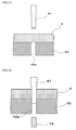
- the solder piece 1A according to this embodiment is configured so as to have a rectangular parallelepiped shape by a punching process in which as shown in FIG. 5A , a calendered solder tape 4 which is a tape like sheet member that is configured so as to have a predetermined thickness is supplied to a die 40 and as shown FIG. 5B , a punch 41 punches out the calendered solder tape 4.
- the calendered solder tape 4 has a thickness that is the same length as that of each side, for example, a length of the side 22a, shared by the first surface 11, the second surface 12, the third surface 13 and the fourth surface 14.
- the punch 41 punching out the calendered solder tape 4 has a section of almost square in this embodiment in which a length of each of the four sides is configured so as to have the almost same length as that of each of the sides in the fifth surface 15 and the sixth surface 16 of the solder piece 1A.
- the die 40 receiving the punch 41 is formed so as to have a passing-through hole 40a through which the solder piece 1A punched out by the punch 41 is passed.
- the passing-through hole 40a has an almost square section in this embodiment, four sides of which are respectively configured so as to have lengths some longer than that of each side of the fifth surface 15 and the sixth surface 16 of the solder piece 1A.
- a precision of the first surface 11, the second surface 12, the third surface 13 and the fourth surface 14, which are shared surfaces, is determined by a clearance between the punch 41 and the die 40 in the passing-through hole 40a. Accordingly, a size of each tool is set so that the first surface 11, the second surface 12, the third surface 13 and the fourth surface 14, which can be the sucked surface, become a desired level by which the solder piece 1A can be sucked using the vacuum suction.
- the chip solder 10A according to this embodiment is configured so as to receive the solder piece 1A in the opened concave portion 30 of the supply tape 3.
- the solder pieces 1A may be received therein with any one of the first surface 11, the second surface 12, the third surface 13 and the fourth surface 14 being exposed from the opened concave portion 30 even if their postures are unchanged and they do not stand in a row.
- solder piece 1A is prevented from being in the supply tape 3 with the fifth surface 15 on which the shear droop portion 15a is formed and the sixth surface that is opposite to the fifth surface 15 being exposed from the opened concave portion 30.
- the chip solder 10A enables any one of the first surface 11, the second surface 12, the third surface 13 and the fourth surface 14, which are configured so as to be a desired level by which the solder piece 1A can be sucked using the vacuum suction, to be a sucked surface, thereby enabling the solder piece 1A to be surely sucked. Further, the chip solder 10A prevents the fifth surface 15 of the solder piece 1A, on which the shear droop portion 15a that is unsuitable for the suction is formed, from being the sucked surface, thereby allowing an occurrence of the failure of suction to be avoided and allowing to be also avoided the failure to supply the solder piece 1A accompanying the failure of suction.
- FIG. 6 is a perspective view of a solder piece according to this embodiment for showing a variation example thereof.
- the solder piece 1B of the variation example is configured with the fifth surface 15 on which the shear droop portion 15a is formed and the sixth surface that is opposite to the fifth surface 15 being rectangles.
- any one of the first surface 11, sides of which are shared by long sides of the fifth surface 15 and the sixth surface 16, and the second surface 12 that is opposite to the first surface 11 becomes an sucked surface.
- the solder piece 1B of the variation example has a size of, as one example, 2.6 mm x 2.0 mm x 0.5 mm.
- This invention is applied to a method of supplementing the solder by mounting a solder piece on a land in addition to a solder paste.
Landscapes
- Engineering & Computer Science (AREA)
- Mechanical Engineering (AREA)
- Manufacturing & Machinery (AREA)
- Microelectronics & Electronic Packaging (AREA)
- Life Sciences & Earth Sciences (AREA)
- Forests & Forestry (AREA)
- Electric Connection Of Electric Components To Printed Circuits (AREA)
- Processing Of Stones Or Stones Resemblance Materials (AREA)
- Punching Or Piercing (AREA)
- Sheet Holders (AREA)
- Packages (AREA)
- Re-Forming, After-Treatment, Cutting And Transporting Of Glass Products (AREA)
- Breeding Of Plants And Reproduction By Means Of Culturing (AREA)
Abstract
Description
- The present invention relates to a solder piece that is used in a soldering process of electronic components mounted on a land on a substrate, a chip solder receiving the solder piece and a method of fabricating the solder piece.
- A soldering technology in which by applying a solder paste to the land formed on the substrate, mounting the electronic components on the solder-paste-applied land of the substrate and melting the solder paste, the soldering is carried out has been conventionally used.
- If a mechanical strength for fixation is required when mounting the electronic components using such a method, an amount of solder may be in short supply by only the solder paste applied to the land.
- Thus, a technology for supplementing the solder by mounting a chipped solder, which is so called as "solder piece", on the land in addition to the solder paste has been proposed (see, for example, Patent Document 1).
- Patent Document 1: Japanese Patent Application Publication No.
H06-275944 - The solder piece is configured so as to become a desired shape by performing a punching process on a sheet member. The solder piece is fabricated by the punching process with a surface thereof including a curved surface, which is so called as "shear droop portion", being formed on a surface which is opposite to a surface pushed by a punch.
- The solder piece thus fabricated is received in an opened concave portion formed in a long supply tape and then, a cover tape is sealed on it, which is then supplied. When mounting the solder piece on the substrate, the solder piece received in the opened concave portion is sucked and maintained by a vacuum suction and is taken out of the supply tape after the cover tape has been removed, so that it is mounted on the substrate.
- When, however, a surface on which the shear droop portion is formed becomes a sucked surface, it may be unable to maintain the solder piece by the suction so that a failure to supply the solder piece may occur.
- The invention solves such a problem, and has an obj ect to provide a solder piece that prevents its surface on which the shear droop portion generated by the punching process is formed from becoming the sucked surface, a chip solder receiving the solder piece and a method of fabricating the solder piece.
- In order to solve the above-mentioned problem, the invention relates to a solder piece that is configured so as to be a rectangular parallelepiped shape by a punching process wherein of four surfaces of the rectangular parallelepiped excluding from surfaces thereof a surface on which the shear droop portion generated by the punching process is formed and a surface that is opposite to the surface on which the shear droop portion is formed, any one surface of at least two opposite surfaces thereof is an sucked surface.
- The invention also relates to a chip solder which contains a solder piece that is configured so as to be a rectangular parallelepiped shape by a punching process and a supply tape in which an opened concave portion that receives the solder piece is formed, wherein of four surfaces the rectangular parallelepiped excluding from surfaces thereof a surface on which the shear droop portion generated by the punching process is formed and a surface that is opposite to the surface on which the shear droop portion is formed, any one surface of at least two opposite surfaces thereof is a sucked surface, and wherein the opened concave portion is configured so as to have a shape such that, of four surfaces of the rectangular parallelepiped excluding from the surfaces thereof the surface on which the shear droop portion is formed and the surface that is opposite to the surface on which the shear droop portion is formed, at least a surface which can be the sucked surface or a surface which is opposite to the surface that can be the sucked surface is exposed.
- Further, the invention relates to a method of fabricating a solder piece that is configured so as to be a rectangular parallelepiped shape by a punching process wherein of four surfaces of the rectangular parallelepiped excluding from surfaces thereof a surface on which the shear droop portion generated by the punching process is formed and a surface that is opposite to the surface on which the shear droop portion is formed, any one surface of at least two opposite surfaces thereof is a sucked surface, the method comprising a step of punching a material with the four surfaces including a surface which can be the sucked surface being shared surfaces.
- According to the invention, the solder piece is configured so as to have a rectangular parallelepiped shape having six surfaces by a punching process. The solder piece is configured so that, of four surfaces of the rectangular parallelepiped excluding a surface on which the shear droop portion generated by the punching process is formed and a surface that is opposite to the surface on which the shear droop portion is formed, any one surface thereof is a sucked surface.
- In the chip solder in which the solder piece is received in the supply tape, the solder piece is not received in the opened concave portion with the surface on which the shear droop portion is formed being exposed but the solder piece is received therein with the surface which can be the sucked surface being exposed from the opened concave portion.
- By the invention, it is possible to prevent the surface on which the shear droop portion generated by the punching process is formed from becoming a sucked surface of the solder piece. This enables the solder piece to be securely sucked, thereby allowing an occurrence of the failure of suction to be avoided and allowing to be also avoided the failure to supply the solder piece accompanying the failure of suction.
-
- [
FIG. 1 ] is a perspective view of a solder piece according to this embodiment for showing an example thereof. - [
FIG. 2 ] is a side view of the solder piece according to this embodiment for showing the example thereof. - [
FIG. 3 ] is a perspective view of a chip solder according to this embodiment for showing an example thereof. - [
FIG. 4A ] is a diagram of the solder piece according to this embodiment for showing an example of use condition thereof. - [
FIG. 4B ] is a diagram of the solder piece according to this embodiment for showing the example of use condition thereof. - [
FIG. 5A ] is an operation diagram of a method of fabricating a solder piece according to this embodiment for showing an example thereof. - [
FIG. 5B ] is an operation diagram of the method of fabricating the solder piece according to this embodiment for showing the example thereof. - [
FIG. 6 ] is a perspective view of a solder piece according to this embodiment for showing a variation example thereof. - The following will describe an embodiment of a solder piece, a chip solder and a method of fabricating the solder piece according to the present invention with reference to drawings.
-
FIG. 1 is a perspective view of the solder piece according to this embodiment for showing an example thereof.FIG. 2 is a side view of the solder piece according to this embodiment for showing the example thereof. - The
solder piece 1A according to this embodiment has a rectangular parallelepiped shape composed of six surfaces and is fabricated by a punching process in which a tape like sheet member is punched out. Thesolder piece 1A is provided with four surfaces or two surfaces which can be an sucked surface on the occasion of handling, in this embodiment, four surfaces of afirst surface 11, asecond surface 12, athird surface 13 and afourth surface 14, afifth surface 15 which is a surface on which ashear droop portion 15a generated by the punching process is formed and asixth surface 16 that is opposite to thefifth surface 15. - The
solder piece 1A is punched out in a direction shown in an arrow A with thefirst surface 11, thesecond surface 12, thethird surface 13 and thefourth surface 14 being shared surfaces. This enables the four surfaces thereof excluding thefifth surface 15 on which theshear droop portion 15a is formed and thesixth surface 16 that is opposite to thefifth surface 15 to be formed with desired size and precision. - Therefore, the
solder piece 1A is configured so that of four surfaces of thefirst surface 11, thesecond surface 12, thethird surface 13 and thefourth surface 14, any one surface of at least two opposite surfaces thereof is the sucked surface but thefifth surface 15 on which theshear droop portion 15a is formed is not any sucked surface. - In this embodiment, the
solder piece 1A is formed with thefifth surface 15 and thesixth surface 16 having almost squares. Aside 20a shared by thefifth surface 15 and thefirst surface 11, aside 20b shared by thefifth surface 15 and thesecond surface 12, aside 20c shared by thefifth surface 15 and thethird surface 13 and aside 20d shared by thefifth surface 15 and thefourth surface 14 are configured so as to have the almost same length within a range which depends on a precision of tool. - Further, the
solder piece 1A is formed so that aside 21a shared by thesixth surface 16 and thefirst surface 11, aside 21b shared by thesixth surface 16 and thesecond surface 12, aside 21c shared by thesixth surface 15 and thethird surface 13 and aside 21d shared by thesixth surface 16 and thefourth surface 14 have the almost same length. Each side of thefifth surface 15 has the almost same length as that of each side of thesixth surface 16. - The
solder piece 1A is formed so that thefirst surface 11, thesecond surface 12, thethird surface 13 and thefourth surface 14 have rectangular shapes. In thesolder piece 1A, aside 22a shared by thefirst surface 11 and thesecond surface 12, aside 22b shared by thesecond surface 12 and thethird surface 13, aside 22c shared by thethird surface 13 and thefourth surface 14 and aside 22d shared by thefourth surface 14 and thefirst surface 11 are configured so as to have the length similar to each other based on a punching-out direction by the punching process. Thesolder piece 1A is formed so that the respective sides shared by thefirst surface 11, thesecond surface 12, thethird surface 13 and thefourth surface 14 are longer than respective sides of thefifth surface 15 and thesixth surface 16. - Thus, in the
solder piece 1A, since thefifth surface 15 and thesixth surface 16 are formed so as to be almost squares and thefirst surface 11, thesecond surface 12, thethird surface 13 and thefourth surface 14 are formed so as to be rectangular, four surfaces of thefirst surface 11, thesecond surface 12, thethird surface 13 and thefourth surface 14 have symmetry with respect to a plane around an axis passing through thefifth surface 15 and thesixth surface 16 as rotation axis. Thesolder piece 1A has a size of, as one example, 1.0 mm x 0.5 mm x 0.5 mm. - Accordingly, the
solder piece 1A is formed with any one surface of thefirst surface 11, thesecond surface 12, thethird surface 13 and thefourth surface 14 being an sucked surface so that thefirst surface 11, thesecond surface 12, thethird surface 13 and thefourth surface 14, which can be the sucked surface, are desired surfaces by which thesolder piece 1A can be sucked using the vacuum suction. -
FIG. 3 is a perspective view of the chip solder according to this embodiment for showing an example thereof. Thechip solder 10A according to this embodiment is provided with thesolder piece 1A thus mentioned above and a supply tape 3 in which the solder piece is received. The supply tape 3 is made of any plastic materials, paper or the like and is formed so as to be long. Plural openedconcave portions 30, each of which is capable of receiving thesolder piece 1A, are formed along an extending direction thereof. Further, thechip solder 10A has feedingholes 31 for allowing the supply tape 3 to be conveyed with them being formed along an extending direction thereof. Thechip solder 10A is sealed by a cover tape, not shown, after thesolder pieces 1A have been received in the openedconcave portions 30. - The opened
concave portions 30 are hollows in each of which itslongitudinal side 30a has a length some longer than that of each side shared by thefirst surface 11, thesecond surface 12, thethird surface 13 and thefourth surface 14 in thesolder piece 1A and itslateral side 30b has a length some longer than that of each side of thefifth surface 15 and thesixth surface 16. The openedconcave portions 30 are hollows in each of which itsdepth side 30c has a depth some dipper than the length of each side of thefifth surface 15 and thesixth surface 16. - Thus, the
chip solder 10A is formed with onesolder piece 1A being received in each of the openedconcave portions 30 in the supply tape 3. Thesolder piece 1A is received therein with an optional posture such that any one surface of thefirst surface 11, thesecond surface 12, thethird surface 13 and thefourth surface 14 is exposed from the openedconcave portion 30 on the axis passing through thefifth surface 15 and thesixth surface 16 as the rotation axis. On the other hand, thesolder piece 1A is prevented from being received in the supply tape 3 under the posture such that any one of thefifth surface 15 on which theshear droop portion 15 is formed and thesixth surface 16 that is opposite to thefifth surface 15 is exposed from the openedconcave portions 30. - Here, if the solder piece has a regular hexahedron shape in which each surface is a square, it can be received in the supply tape even in a posture such that a surface on which the shear droop portion is formed is exposed from the opened concave portions of the supply tape. Accordingly, the solder piece is configured so as to be a rectangular parallelepiped shape.
-
FIGS. 4A and 4B are diagrams of the solder pieces according to this embodiment each showing an example of use condition thereof. As shown inFIG. 4A , thesolder piece 1A is mounted together with anelectronic component 53 on aland 52 of asubstrate 51, to which asolder paste 50 is applied. In a step of mounting thesolder piece 1A on thesubstrate 51, thesolder piece 1A supplied in a form of thechip solder 10A is sucked by the vacuum suction and mounted on the predetermined land. - By putting the
substrate 51 into a reflow furnace, not shown, and heating it, thesolder paste 50 and thesolder piece 1A are then melted together, as shown inFIG. 4B , which allows theelectronic component 53 to be soldered. - The soldering using the
solder piece 1A enables an amount of solder to be increased as compared with the soldering using only the solder paste, which allows to be improved a strength of a soldered portion in which any mechanical strength is required. -
FIGS. 5A and 5B are operation diagrams of a method of fabricating the solder piece according to this embodiment for showing an example thereof. The following will then describe the method of fabricating the solder piece according to this embodiment with reference to the drawings. Thesolder piece 1A according to this embodiment is configured so as to have a rectangular parallelepiped shape by a punching process in which as shown inFIG. 5A , acalendered solder tape 4 which is a tape like sheet member that is configured so as to have a predetermined thickness is supplied to adie 40 and as shownFIG. 5B , apunch 41 punches out thecalendered solder tape 4. - In the
solder piece 1A, a punching direction in the punching process is set so that thefirst surface 11, thesecond surface 12, thethird surface 13 and thefourth surface 14 are shared surfaces. Thus, thecalendered solder tape 4 has a thickness that is the same length as that of each side, for example, a length of theside 22a, shared by thefirst surface 11, thesecond surface 12, thethird surface 13 and thefourth surface 14. - The
punch 41 punching out thecalendered solder tape 4 has a section of almost square in this embodiment in which a length of each of the four sides is configured so as to have the almost same length as that of each of the sides in thefifth surface 15 and thesixth surface 16 of thesolder piece 1A. - The die 40 receiving the
punch 41 is formed so as to have a passing-throughhole 40a through which thesolder piece 1A punched out by thepunch 41 is passed. The passing-throughhole 40a has an almost square section in this embodiment, four sides of which are respectively configured so as to have lengths some longer than that of each side of thefifth surface 15 and thesixth surface 16 of thesolder piece 1A. - In the
solder piece 1A fabricated by the punching process, a precision of thefirst surface 11, thesecond surface 12, thethird surface 13 and thefourth surface 14, which are shared surfaces, is determined by a clearance between thepunch 41 and the die 40 in the passing-throughhole 40a. Accordingly, a size of each tool is set so that thefirst surface 11, thesecond surface 12, thethird surface 13 and thefourth surface 14, which can be the sucked surface, become a desired level by which thesolder piece 1A can be sucked using the vacuum suction. - The following will then describe an example of the method of fabricating a chip solder according to this embodiment with reference to the drawings. The
chip solder 10A according to this embodiment is configured so as to receive thesolder piece 1A in the openedconcave portion 30 of the supply tape 3. - Based on the shape of each of the
solder piece 1A and the shape of the openedconcave portion 30 of the supply tape 3, thesolder pieces 1A may be received therein with any one of thefirst surface 11, thesecond surface 12, thethird surface 13 and thefourth surface 14 being exposed from the openedconcave portion 30 even if their postures are unchanged and they do not stand in a row. - On the other hand, the
solder piece 1A is prevented from being in the supply tape 3 with thefifth surface 15 on which theshear droop portion 15a is formed and the sixth surface that is opposite to thefifth surface 15 being exposed from the openedconcave portion 30. - Accordingly, the
chip solder 10A enables any one of thefirst surface 11, thesecond surface 12, thethird surface 13 and thefourth surface 14, which are configured so as to be a desired level by which thesolder piece 1A can be sucked using the vacuum suction, to be a sucked surface, thereby enabling thesolder piece 1A to be surely sucked. Further, thechip solder 10A prevents thefifth surface 15 of thesolder piece 1A, on which theshear droop portion 15a that is unsuitable for the suction is formed, from being the sucked surface, thereby allowing an occurrence of the failure of suction to be avoided and allowing to be also avoided the failure to supply thesolder piece 1A accompanying the failure of suction. -
FIG. 6 is a perspective view of a solder piece according to this embodiment for showing a variation example thereof. The solder piece 1B of the variation example is configured with thefifth surface 15 on which theshear droop portion 15a is formed and the sixth surface that is opposite to thefifth surface 15 being rectangles. In the shape of the solder piece 1B of the variation example, for example, any one of thefirst surface 11, sides of which are shared by long sides of thefifth surface 15 and thesixth surface 16, and thesecond surface 12 that is opposite to thefirst surface 11 becomes an sucked surface. The solder piece 1B of the variation example has a size of, as one example, 2.6 mm x 2.0 mm x 0.5 mm. - This invention is applied to a method of supplementing the solder by mounting a solder piece on a land in addition to a solder paste. Description of Codes
- 1A, 1B...Solder Piece; 11...First surface; 12...Second Surface; 13...Third Surface; 14...Fourth Surface; 15...Fifth Surface; 16...Sixth Surface; 10A...Chip Solder; 3...Supply Tape; 30... Opened Concave Portion.
Claims (5)
- A solder piece that is configured so as to be a rectangular parallelepiped shape by a punching process, characterized in that,
of four surfaces of the rectangular parallelepiped excluding from surfaces thereof a surface on which the shear droop portion generated by the punching process is formed and a surface that is opposite to the surface on which the shear droop portion is formed, any one surface of at least two opposite surfaces thereof is an sucked surface. - The solder piece according to Claim 1, characterized in that a surface which can be the sucked surface is configured so as to have an area larger than any of the surface on which the shear droop portion is formed and the surface that is opposite to the surface on which the shear droop portion is formed.
- The solder piece according to Claim 1 or 2, characterized in that the four surfaces including the surface which can be the sucked surface are configured so as to have a length of longitudinal side there longer than that of each side of any of the surface on which the shear droop portion is formed and the surface that is opposite to the surface on which the shear droop portion is formed.
- A chip solder which contains:a solder piece that is configured so as to be a rectangular parallelepiped shape by a punching process; anda supply tape in which an opened concave portion that receives the solder piece is formed, characterized in that,of four surfaces of the rectangular parallelepiped excluding from surfaces thereof a surface thereof on which the shear droop portion generated by the punching process is formed and a surface thereof that is opposite to the surface thereof on which the shear droop portion is formed, any one surface of at least two opposite surfaces thereof is a sucked surface, andthe opened concave portion is configured so as to have a shape such that, of four surfaces of the rectangular parallelepiped excluding from the surfaces thereof the surface on which the shear droop portion is formed and the surface that is opposite to the surface thereof on which the shear droop portion is formed, at least a surface which can be the sucked surface or a surface which is opposite to the surface that can be the sucked surface is exposed.
- A method of fabricating a solder piece that is configured so as to be a rectangular parallelepiped shape by a punching process, characterized in that, of four surfaces of the rectangular parallelepiped excluding from surfaces thereof excluding a surface on which the shear droop portion generated by the punching process is formed and a surface that is opposite to the surface thereof on which the shear droop portion is formed, any one surface of at least two opposite surfaces thereof is a sucked surface, and the method comprises a step of punching a material with the four surfaces including a surface which can be the sucked surface being shared surfaces.
Priority Applications (2)
| Application Number | Priority Date | Filing Date | Title |
|---|---|---|---|
| HUE11808554A HUE035183T2 (en) | 2011-09-30 | 2011-09-30 | Solder piece, chip solder, and method for manufacturing a chip solder |
| PL11808554T PL2749374T3 (en) | 2011-09-30 | 2011-09-30 | Solder piece, chip solder, and method for manufacturing a chip solder |
Applications Claiming Priority (1)
| Application Number | Priority Date | Filing Date | Title |
|---|---|---|---|
| PCT/JP2011/072622 WO2013046450A1 (en) | 2011-09-30 | 2011-09-30 | Solder piece, chip solder, and method for manufacturing solder piece |
Publications (3)
| Publication Number | Publication Date |
|---|---|
| EP2749374A1 true EP2749374A1 (en) | 2014-07-02 |
| EP2749374A4 EP2749374A4 (en) | 2015-07-01 |
| EP2749374B1 EP2749374B1 (en) | 2017-08-09 |
Family
ID=46498768
Family Applications (1)
| Application Number | Title | Priority Date | Filing Date |
|---|---|---|---|
| EP11808554.7A Active EP2749374B1 (en) | 2011-09-30 | 2011-09-30 | Solder piece, chip solder, and method for manufacturing a chip solder |
Country Status (12)
| Country | Link |
|---|---|
| US (3) | US8991679B2 (en) |
| EP (1) | EP2749374B1 (en) |
| JP (1) | JP4952869B1 (en) |
| KR (1) | KR101164396B1 (en) |
| CN (1) | CN102612867B (en) |
| CY (1) | CY1119735T1 (en) |
| ES (1) | ES2640319T3 (en) |
| HU (1) | HUE035183T2 (en) |
| PL (1) | PL2749374T3 (en) |
| PT (1) | PT2749374T (en) |
| TW (1) | TWI388391B (en) |
| WO (1) | WO2013046450A1 (en) |
Families Citing this family (4)
| Publication number | Priority date | Publication date | Assignee | Title |
|---|---|---|---|---|
| EP2749374B1 (en) * | 2011-09-30 | 2017-08-09 | Senju Metal Industry Co., Ltd | Solder piece, chip solder, and method for manufacturing a chip solder |
| JP6327873B2 (en) * | 2014-02-03 | 2018-05-23 | ウツミ電気株式会社 | Solder piece, chip solder, and method of manufacturing solder piece |
| US20170203380A1 (en) * | 2016-01-20 | 2017-07-20 | Indium Corporation | Capillary block |
| US20240157431A1 (en) * | 2022-08-11 | 2024-05-16 | Joinset Co., Ltd. | Method for making non-spherical solder ball |
Family Cites Families (11)
| Publication number | Priority date | Publication date | Assignee | Title |
|---|---|---|---|---|
| JPS61172697A (en) * | 1985-01-28 | 1986-08-04 | Victor Co Of Japan Ltd | Solder assemblage |
| US4712721A (en) * | 1986-03-17 | 1987-12-15 | Raychem Corp. | Solder delivery systems |
| JPS6411095A (en) * | 1987-10-30 | 1989-01-13 | Anritsu Corp | Production of granular solder |
| JPH06275944A (en) | 1993-03-22 | 1994-09-30 | Sharp Corp | Soldering method |
| JPH06283536A (en) * | 1993-03-30 | 1994-10-07 | Nec Corp | Solder bump mounting board |
| JPH09219580A (en) * | 1996-02-09 | 1997-08-19 | Fuji Xerox Co Ltd | Solder feeder device and method |
| US6426564B1 (en) * | 1999-02-24 | 2002-07-30 | Micron Technology, Inc. | Recessed tape and method for forming a BGA assembly |
| US6929170B2 (en) * | 2003-09-30 | 2005-08-16 | Ted Ju | Solder deposition method |
| US7533793B2 (en) * | 2004-02-20 | 2009-05-19 | Fry's Metals, Inc. | Solder preforms for use in electronic assembly |
| JP2005294035A (en) | 2004-03-31 | 2005-10-20 | Matsushita Electric Works Ltd | Connector |
| EP2749374B1 (en) * | 2011-09-30 | 2017-08-09 | Senju Metal Industry Co., Ltd | Solder piece, chip solder, and method for manufacturing a chip solder |
-
2011
- 2011-09-30 EP EP11808554.7A patent/EP2749374B1/en active Active
- 2011-09-30 WO PCT/JP2011/072622 patent/WO2013046450A1/en not_active Ceased
- 2011-09-30 PT PT118085547T patent/PT2749374T/en unknown
- 2011-09-30 PL PL11808554T patent/PL2749374T3/en unknown
- 2011-09-30 ES ES11808554.7T patent/ES2640319T3/en active Active
- 2011-09-30 KR KR1020127007306A patent/KR101164396B1/en active Active
- 2011-09-30 HU HUE11808554A patent/HUE035183T2/en unknown
- 2011-09-30 CN CN2011800043961A patent/CN102612867B/en active Active
- 2011-09-30 US US13/501,746 patent/US8991679B2/en active Active
- 2011-09-30 JP JP2012501488A patent/JP4952869B1/en active Active
-
2012
- 2012-04-16 TW TW101113419A patent/TWI388391B/en active
-
2015
- 2015-01-15 US US14/598,007 patent/US9327364B2/en active Active
-
2016
- 2016-03-21 US US15/075,602 patent/US20160199946A1/en not_active Abandoned
-
2017
- 2017-11-07 CY CY20171101165T patent/CY1119735T1/en unknown
Also Published As
| Publication number | Publication date |
|---|---|
| US20130082087A1 (en) | 2013-04-04 |
| PL2749374T3 (en) | 2018-01-31 |
| JPWO2013046450A1 (en) | 2015-03-26 |
| WO2013046450A1 (en) | 2013-04-04 |
| CY1119735T1 (en) | 2018-06-27 |
| CN102612867B (en) | 2013-11-27 |
| HUE035183T2 (en) | 2018-05-02 |
| US20150122874A1 (en) | 2015-05-07 |
| EP2749374B1 (en) | 2017-08-09 |
| US8991679B2 (en) | 2015-03-31 |
| PT2749374T (en) | 2017-10-03 |
| ES2640319T3 (en) | 2017-11-02 |
| TWI388391B (en) | 2013-03-11 |
| KR101164396B1 (en) | 2012-07-09 |
| JP4952869B1 (en) | 2012-06-13 |
| US9327364B2 (en) | 2016-05-03 |
| CN102612867A (en) | 2012-07-25 |
| US20160199946A1 (en) | 2016-07-14 |
| EP2749374A4 (en) | 2015-07-01 |
| TW201235147A (en) | 2012-09-01 |
Similar Documents
| Publication | Publication Date | Title |
|---|---|---|
| US9327364B2 (en) | Solder piece, chip solder and method of fabricating solder piece | |
| JP2011187196A (en) | Press-fit terminal | |
| US20140118973A1 (en) | Pin header assembly and method of forming the same | |
| JP5790633B2 (en) | Carrier tape, packaging tape and electronic components | |
| US20070173134A1 (en) | Fixing member and fixing structure | |
| EP3822997A1 (en) | Busbar laminate, electronic component mounting module including same, and method of manufacturing busbar laminate | |
| US7378728B2 (en) | Electronic component mounting package and package assembled substrate | |
| JP3190099U (en) | Solder pieces and chip solder | |
| JP6327873B2 (en) | Solder piece, chip solder, and method of manufacturing solder piece | |
| JP4835258B2 (en) | Electronic component packaging | |
| JP6838961B2 (en) | Wiring board and its manufacturing method | |
| JP3465901B1 (en) | Mounting board | |
| CN102626832B (en) | Method for making an opening in a substrate | |
| JP2019061883A (en) | Method of manufacturing connector | |
| EP2781144B1 (en) | Fabrication of three-dimensional printed circuit board structures | |
| CN100415610C (en) | Method of making paper carrier strip | |
| JP6441266B2 (en) | Manufacturing method of member with composite terminal and member with composite terminal | |
| JP2011054528A (en) | Terminal fitting | |
| JP2015012214A (en) | Transfer jig and manufacturing method of electronic component using the same | |
| EP3554201A1 (en) | Method and device for processing a radial electronic component | |
| CN210298416U (en) | Array-arranged electronic element and surface mounting system thereof | |
| JP4279262B2 (en) | Manufacturing method of substrate with terminal | |
| JP6904734B2 (en) | Electrical connector and its manufacturing method | |
| JP2018113405A (en) | Printed wiring board and electronic circuit board | |
| JP5997627B2 (en) | Temporary fixing method of conductive member and solder sheet |
Legal Events
| Date | Code | Title | Description |
|---|---|---|---|
| PUAI | Public reference made under article 153(3) epc to a published international application that has entered the european phase |
Free format text: ORIGINAL CODE: 0009012 |
|
| 17P | Request for examination filed |
Effective date: 20120127 |
|
| AK | Designated contracting states |
Kind code of ref document: A1 Designated state(s): AL AT BE BG CH CY CZ DE DK EE ES FI FR GB GR HR HU IE IS IT LI LT LU LV MC MK MT NL NO PL PT RO RS SE SI SK SM TR |
|
| DAX | Request for extension of the european patent (deleted) | ||
| RA4 | Supplementary search report drawn up and despatched (corrected) |
Effective date: 20150601 |
|
| RIC1 | Information provided on ipc code assigned before grant |
Ipc: B23K 35/40 20060101ALI20150526BHEP Ipc: H05K 3/34 20060101ALI20150526BHEP Ipc: B23K 35/14 20060101AFI20150526BHEP |
|
| 17Q | First examination report despatched |
Effective date: 20160624 |
|
| REG | Reference to a national code |
Ref country code: DE Ref legal event code: R079 Ref document number: 602011040482 Country of ref document: DE Free format text: PREVIOUS MAIN CLASS: B23K0035140000 Ipc: B23K0001000000 |
|
| GRAP | Despatch of communication of intention to grant a patent |
Free format text: ORIGINAL CODE: EPIDOSNIGR1 |
|
| STAA | Information on the status of an ep patent application or granted ep patent |
Free format text: STATUS: GRANT OF PATENT IS INTENDED |
|
| RIC1 | Information provided on ipc code assigned before grant |
Ipc: B23K 35/30 20060101ALI20170127BHEP Ipc: B23K 1/008 20060101ALI20170127BHEP Ipc: B23K 35/32 20060101ALI20170127BHEP Ipc: B23K 35/40 20060101ALI20170127BHEP Ipc: B26F 1/02 20060101ALI20170127BHEP Ipc: B23K 1/00 20060101AFI20170127BHEP Ipc: B23K 3/06 20060101ALI20170127BHEP Ipc: B23K 101/42 20060101ALI20170127BHEP Ipc: B23K 35/28 20060101ALI20170127BHEP Ipc: B23K 35/02 20060101ALI20170127BHEP Ipc: B23K 35/26 20060101ALI20170127BHEP Ipc: H05K 3/34 20060101ALI20170127BHEP |
|
| INTG | Intention to grant announced |
Effective date: 20170227 |
|
| RIN1 | Information on inventor provided before grant (corrected) |
Inventor name: WATANABE KOJI Inventor name: ITO MASAYA Inventor name: KANNO MASAHIKO Inventor name: TAKAHASHI HIDEAKI Inventor name: ABE MASAHIKO |
|
| GRAS | Grant fee paid |
Free format text: ORIGINAL CODE: EPIDOSNIGR3 |
|
| GRAA | (expected) grant |
Free format text: ORIGINAL CODE: 0009210 |
|
| STAA | Information on the status of an ep patent application or granted ep patent |
Free format text: STATUS: THE PATENT HAS BEEN GRANTED |
|
| AK | Designated contracting states |
Kind code of ref document: B1 Designated state(s): AL AT BE BG CH CY CZ DE DK EE ES FI FR GB GR HR HU IE IS IT LI LT LU LV MC MK MT NL NO PL PT RO RS SE SI SK SM TR |
|
| REG | Reference to a national code |
Ref country code: GB Ref legal event code: FG4D |
|
| REG | Reference to a national code |
Ref country code: AT Ref legal event code: REF Ref document number: 916282 Country of ref document: AT Kind code of ref document: T Effective date: 20170815 Ref country code: CH Ref legal event code: EP |
|
| REG | Reference to a national code |
Ref country code: FR Ref legal event code: PLFP Year of fee payment: 7 |
|
| REG | Reference to a national code |
Ref country code: IE Ref legal event code: FG4D |
|
| REG | Reference to a national code |
Ref country code: DE Ref legal event code: R096 Ref document number: 602011040482 Country of ref document: DE |
|
| REG | Reference to a national code |
Ref country code: PT Ref legal event code: SC4A Ref document number: 2749374 Country of ref document: PT Date of ref document: 20171003 Kind code of ref document: T Free format text: AVAILABILITY OF NATIONAL TRANSLATION Effective date: 20170925 |
|
| REG | Reference to a national code |
Ref country code: ES Ref legal event code: FG2A Ref document number: 2640319 Country of ref document: ES Kind code of ref document: T3 Effective date: 20171102 |
|
| REG | Reference to a national code |
Ref country code: NL Ref legal event code: FP |
|
| REG | Reference to a national code |
Ref country code: SE Ref legal event code: TRGR |
|
| REG | Reference to a national code |
Ref country code: LT Ref legal event code: MG4D |
|
| REG | Reference to a national code |
Ref country code: AT Ref legal event code: MK05 Ref document number: 916282 Country of ref document: AT Kind code of ref document: T Effective date: 20170809 |
|
| PG25 | Lapsed in a contracting state [announced via postgrant information from national office to epo] |
Ref country code: LT Free format text: LAPSE BECAUSE OF FAILURE TO SUBMIT A TRANSLATION OF THE DESCRIPTION OR TO PAY THE FEE WITHIN THE PRESCRIBED TIME-LIMIT Effective date: 20170809 Ref country code: FI Free format text: LAPSE BECAUSE OF FAILURE TO SUBMIT A TRANSLATION OF THE DESCRIPTION OR TO PAY THE FEE WITHIN THE PRESCRIBED TIME-LIMIT Effective date: 20170809 Ref country code: HR Free format text: LAPSE BECAUSE OF FAILURE TO SUBMIT A TRANSLATION OF THE DESCRIPTION OR TO PAY THE FEE WITHIN THE PRESCRIBED TIME-LIMIT Effective date: 20170809 Ref country code: NO Free format text: LAPSE BECAUSE OF FAILURE TO SUBMIT A TRANSLATION OF THE DESCRIPTION OR TO PAY THE FEE WITHIN THE PRESCRIBED TIME-LIMIT Effective date: 20171109 Ref country code: AT Free format text: LAPSE BECAUSE OF FAILURE TO SUBMIT A TRANSLATION OF THE DESCRIPTION OR TO PAY THE FEE WITHIN THE PRESCRIBED TIME-LIMIT Effective date: 20170809 |
|
| PG25 | Lapsed in a contracting state [announced via postgrant information from national office to epo] |
Ref country code: LV Free format text: LAPSE BECAUSE OF FAILURE TO SUBMIT A TRANSLATION OF THE DESCRIPTION OR TO PAY THE FEE WITHIN THE PRESCRIBED TIME-LIMIT Effective date: 20170809 Ref country code: IS Free format text: LAPSE BECAUSE OF FAILURE TO SUBMIT A TRANSLATION OF THE DESCRIPTION OR TO PAY THE FEE WITHIN THE PRESCRIBED TIME-LIMIT Effective date: 20171209 Ref country code: BG Free format text: LAPSE BECAUSE OF FAILURE TO SUBMIT A TRANSLATION OF THE DESCRIPTION OR TO PAY THE FEE WITHIN THE PRESCRIBED TIME-LIMIT Effective date: 20171109 Ref country code: GR Free format text: LAPSE BECAUSE OF FAILURE TO SUBMIT A TRANSLATION OF THE DESCRIPTION OR TO PAY THE FEE WITHIN THE PRESCRIBED TIME-LIMIT Effective date: 20171110 Ref country code: RS Free format text: LAPSE BECAUSE OF FAILURE TO SUBMIT A TRANSLATION OF THE DESCRIPTION OR TO PAY THE FEE WITHIN THE PRESCRIBED TIME-LIMIT Effective date: 20170809 |
|
| PG25 | Lapsed in a contracting state [announced via postgrant information from national office to epo] |
Ref country code: DK Free format text: LAPSE BECAUSE OF FAILURE TO SUBMIT A TRANSLATION OF THE DESCRIPTION OR TO PAY THE FEE WITHIN THE PRESCRIBED TIME-LIMIT Effective date: 20170809 Ref country code: RO Free format text: LAPSE BECAUSE OF FAILURE TO SUBMIT A TRANSLATION OF THE DESCRIPTION OR TO PAY THE FEE WITHIN THE PRESCRIBED TIME-LIMIT Effective date: 20170809 |
|
| REG | Reference to a national code |
Ref country code: CH Ref legal event code: PL |
|
| REG | Reference to a national code |
Ref country code: HU Ref legal event code: AG4A Ref document number: E035183 Country of ref document: HU |
|
| REG | Reference to a national code |
Ref country code: DE Ref legal event code: R097 Ref document number: 602011040482 Country of ref document: DE |
|
| PG25 | Lapsed in a contracting state [announced via postgrant information from national office to epo] |
Ref country code: SK Free format text: LAPSE BECAUSE OF FAILURE TO SUBMIT A TRANSLATION OF THE DESCRIPTION OR TO PAY THE FEE WITHIN THE PRESCRIBED TIME-LIMIT Effective date: 20170809 Ref country code: EE Free format text: LAPSE BECAUSE OF FAILURE TO SUBMIT A TRANSLATION OF THE DESCRIPTION OR TO PAY THE FEE WITHIN THE PRESCRIBED TIME-LIMIT Effective date: 20170809 Ref country code: SM Free format text: LAPSE BECAUSE OF FAILURE TO SUBMIT A TRANSLATION OF THE DESCRIPTION OR TO PAY THE FEE WITHIN THE PRESCRIBED TIME-LIMIT Effective date: 20170809 Ref country code: MC Free format text: LAPSE BECAUSE OF FAILURE TO SUBMIT A TRANSLATION OF THE DESCRIPTION OR TO PAY THE FEE WITHIN THE PRESCRIBED TIME-LIMIT Effective date: 20170809 |
|
| PLBE | No opposition filed within time limit |
Free format text: ORIGINAL CODE: 0009261 |
|
| STAA | Information on the status of an ep patent application or granted ep patent |
Free format text: STATUS: NO OPPOSITION FILED WITHIN TIME LIMIT |
|
| REG | Reference to a national code |
Ref country code: IE Ref legal event code: MM4A |
|
| PG25 | Lapsed in a contracting state [announced via postgrant information from national office to epo] |
Ref country code: LU Free format text: LAPSE BECAUSE OF NON-PAYMENT OF DUE FEES Effective date: 20170930 |
|
| 26N | No opposition filed |
Effective date: 20180511 |
|
| PG25 | Lapsed in a contracting state [announced via postgrant information from national office to epo] |
Ref country code: IE Free format text: LAPSE BECAUSE OF NON-PAYMENT OF DUE FEES Effective date: 20170930 Ref country code: LI Free format text: LAPSE BECAUSE OF NON-PAYMENT OF DUE FEES Effective date: 20170930 Ref country code: CH Free format text: LAPSE BECAUSE OF NON-PAYMENT OF DUE FEES Effective date: 20170930 |
|
| REG | Reference to a national code |
Ref country code: FR Ref legal event code: PLFP Year of fee payment: 8 |
|
| PG25 | Lapsed in a contracting state [announced via postgrant information from national office to epo] |
Ref country code: SI Free format text: LAPSE BECAUSE OF FAILURE TO SUBMIT A TRANSLATION OF THE DESCRIPTION OR TO PAY THE FEE WITHIN THE PRESCRIBED TIME-LIMIT Effective date: 20170809 |
|
| PG25 | Lapsed in a contracting state [announced via postgrant information from national office to epo] |
Ref country code: MT Free format text: LAPSE BECAUSE OF NON-PAYMENT OF DUE FEES Effective date: 20170930 |
|
| PG25 | Lapsed in a contracting state [announced via postgrant information from national office to epo] |
Ref country code: MK Free format text: LAPSE BECAUSE OF FAILURE TO SUBMIT A TRANSLATION OF THE DESCRIPTION OR TO PAY THE FEE WITHIN THE PRESCRIBED TIME-LIMIT Effective date: 20170809 |
|
| PG25 | Lapsed in a contracting state [announced via postgrant information from national office to epo] |
Ref country code: TR Free format text: LAPSE BECAUSE OF FAILURE TO SUBMIT A TRANSLATION OF THE DESCRIPTION OR TO PAY THE FEE WITHIN THE PRESCRIBED TIME-LIMIT Effective date: 20170809 |
|
| PG25 | Lapsed in a contracting state [announced via postgrant information from national office to epo] |
Ref country code: AL Free format text: LAPSE BECAUSE OF FAILURE TO SUBMIT A TRANSLATION OF THE DESCRIPTION OR TO PAY THE FEE WITHIN THE PRESCRIBED TIME-LIMIT Effective date: 20170809 |
|
| P01 | Opt-out of the competence of the unified patent court (upc) registered |
Effective date: 20230609 |
|
| PGFP | Annual fee paid to national office [announced via postgrant information from national office to epo] |
Ref country code: NL Payment date: 20250814 Year of fee payment: 15 |
|
| PGFP | Annual fee paid to national office [announced via postgrant information from national office to epo] |
Ref country code: PT Payment date: 20250926 Year of fee payment: 15 |
|
| PGFP | Annual fee paid to national office [announced via postgrant information from national office to epo] |
Ref country code: DE Payment date: 20250805 Year of fee payment: 15 |
|
| PGFP | Annual fee paid to national office [announced via postgrant information from national office to epo] |
Ref country code: PL Payment date: 20250728 Year of fee payment: 15 Ref country code: IT Payment date: 20250825 Year of fee payment: 15 |
|
| PGFP | Annual fee paid to national office [announced via postgrant information from national office to epo] |
Ref country code: HU Payment date: 20250828 Year of fee payment: 15 Ref country code: BE Payment date: 20250818 Year of fee payment: 15 Ref country code: GB Payment date: 20250807 Year of fee payment: 15 |
|
| PGFP | Annual fee paid to national office [announced via postgrant information from national office to epo] |
Ref country code: FR Payment date: 20250808 Year of fee payment: 15 |
|
| PGFP | Annual fee paid to national office [announced via postgrant information from national office to epo] |
Ref country code: SE Payment date: 20250812 Year of fee payment: 15 |
|
| PGFP | Annual fee paid to national office [announced via postgrant information from national office to epo] |
Ref country code: CZ Payment date: 20250923 Year of fee payment: 15 |
|
| PGFP | Annual fee paid to national office [announced via postgrant information from national office to epo] |
Ref country code: CY Payment date: 20250911 Year of fee payment: 15 |
|
| PGFP | Annual fee paid to national office [announced via postgrant information from national office to epo] |
Ref country code: ES Payment date: 20251013 Year of fee payment: 15 |