EP2717452B1 - Dispositif de conversion de puissance - Google Patents
Dispositif de conversion de puissance Download PDFInfo
- Publication number
- EP2717452B1 EP2717452B1 EP12792428.0A EP12792428A EP2717452B1 EP 2717452 B1 EP2717452 B1 EP 2717452B1 EP 12792428 A EP12792428 A EP 12792428A EP 2717452 B1 EP2717452 B1 EP 2717452B1
- Authority
- EP
- European Patent Office
- Prior art keywords
- switching elements
- condensers
- bidirectional switching
- bus bars
- power
- Prior art date
- Legal status (The legal status is an assumption and is not a legal conclusion. Google has not performed a legal analysis and makes no representation as to the accuracy of the status listed.)
- Active
Links
- 238000006243 chemical reaction Methods 0.000 title description 14
- 230000002457 bidirectional effect Effects 0.000 description 121
- 229910001219 R-phase Inorganic materials 0.000 description 14
- 230000018199 S phase Effects 0.000 description 11
- 238000000034 method Methods 0.000 description 7
- 238000010276 construction Methods 0.000 description 3
- 238000009499 grossing Methods 0.000 description 3
- 230000004048 modification Effects 0.000 description 3
- 238000012986 modification Methods 0.000 description 3
- 238000010586 diagram Methods 0.000 description 2
- RYGMFSIKBFXOCR-UHFFFAOYSA-N Copper Chemical compound [Cu] RYGMFSIKBFXOCR-UHFFFAOYSA-N 0.000 description 1
- 229910052802 copper Inorganic materials 0.000 description 1
- 239000010949 copper Substances 0.000 description 1
- 230000009977 dual effect Effects 0.000 description 1
- 230000000694 effects Effects 0.000 description 1
- 239000011810 insulating material Substances 0.000 description 1
- 239000011159 matrix material Substances 0.000 description 1
- 238000010992 reflux Methods 0.000 description 1
- 239000004065 semiconductor Substances 0.000 description 1
- 239000000758 substrate Substances 0.000 description 1
- 230000001629 suppression Effects 0.000 description 1
- 238000011144 upstream manufacturing Methods 0.000 description 1
Images


Classifications
-
- H—ELECTRICITY
- H02—GENERATION; CONVERSION OR DISTRIBUTION OF ELECTRIC POWER
- H02M—APPARATUS FOR CONVERSION BETWEEN AC AND AC, BETWEEN AC AND DC, OR BETWEEN DC AND DC, AND FOR USE WITH MAINS OR SIMILAR POWER SUPPLY SYSTEMS; CONVERSION OF DC OR AC INPUT POWER INTO SURGE OUTPUT POWER; CONTROL OR REGULATION THEREOF
- H02M5/00—Conversion of ac power input into ac power output, e.g. for change of voltage, for change of frequency, for change of number of phases
- H02M5/02—Conversion of ac power input into ac power output, e.g. for change of voltage, for change of frequency, for change of number of phases without intermediate conversion into dc
- H02M5/04—Conversion of ac power input into ac power output, e.g. for change of voltage, for change of frequency, for change of number of phases without intermediate conversion into dc by static converters
- H02M5/22—Conversion of ac power input into ac power output, e.g. for change of voltage, for change of frequency, for change of number of phases without intermediate conversion into dc by static converters using discharge tubes with control electrode or semiconductor devices with control electrode
- H02M5/275—Conversion of ac power input into ac power output, e.g. for change of voltage, for change of frequency, for change of number of phases without intermediate conversion into dc by static converters using discharge tubes with control electrode or semiconductor devices with control electrode using devices of a triode or transistor type requiring continuous application of a control signal
- H02M5/293—Conversion of ac power input into ac power output, e.g. for change of voltage, for change of frequency, for change of number of phases without intermediate conversion into dc by static converters using discharge tubes with control electrode or semiconductor devices with control electrode using devices of a triode or transistor type requiring continuous application of a control signal using semiconductor devices only
-
- H—ELECTRICITY
- H02—GENERATION; CONVERSION OR DISTRIBUTION OF ELECTRIC POWER
- H02M—APPARATUS FOR CONVERSION BETWEEN AC AND AC, BETWEEN AC AND DC, OR BETWEEN DC AND DC, AND FOR USE WITH MAINS OR SIMILAR POWER SUPPLY SYSTEMS; CONVERSION OF DC OR AC INPUT POWER INTO SURGE OUTPUT POWER; CONTROL OR REGULATION THEREOF
- H02M7/00—Conversion of ac power input into dc power output; Conversion of dc power input into ac power output
- H02M7/003—Constructional details, e.g. physical layout, assembly, wiring or busbar connections
-
- H—ELECTRICITY
- H05—ELECTRIC TECHNIQUES NOT OTHERWISE PROVIDED FOR
- H05K—PRINTED CIRCUITS; CASINGS OR CONSTRUCTIONAL DETAILS OF ELECTRIC APPARATUS; MANUFACTURE OF ASSEMBLAGES OF ELECTRICAL COMPONENTS
- H05K7/00—Constructional details common to different types of electric apparatus
- H05K7/14—Mounting supporting structure in casing or on frame or rack
- H05K7/1422—Printed circuit boards receptacles, e.g. stacked structures, electronic circuit modules or box like frames
- H05K7/1427—Housings
- H05K7/1432—Housings specially adapted for power drive units or power converters
- H05K7/14329—Housings specially adapted for power drive units or power converters specially adapted for the configuration of power bus bars
-
- H—ELECTRICITY
- H02—GENERATION; CONVERSION OR DISTRIBUTION OF ELECTRIC POWER
- H02M—APPARATUS FOR CONVERSION BETWEEN AC AND AC, BETWEEN AC AND DC, OR BETWEEN DC AND DC, AND FOR USE WITH MAINS OR SIMILAR POWER SUPPLY SYSTEMS; CONVERSION OF DC OR AC INPUT POWER INTO SURGE OUTPUT POWER; CONTROL OR REGULATION THEREOF
- H02M1/00—Details of apparatus for conversion
- H02M1/42—Circuits or arrangements for compensating for or adjusting power factor in converters or inverters
- H02M1/4208—Arrangements for improving power factor of AC input
- H02M1/4258—Arrangements for improving power factor of AC input using a single converter stage both for correction of AC input power factor and generation of a regulated and galvanically isolated DC output voltage
-
- Y—GENERAL TAGGING OF NEW TECHNOLOGICAL DEVELOPMENTS; GENERAL TAGGING OF CROSS-SECTIONAL TECHNOLOGIES SPANNING OVER SEVERAL SECTIONS OF THE IPC; TECHNICAL SUBJECTS COVERED BY FORMER USPC CROSS-REFERENCE ART COLLECTIONS [XRACs] AND DIGESTS
- Y02—TECHNOLOGIES OR APPLICATIONS FOR MITIGATION OR ADAPTATION AGAINST CLIMATE CHANGE
- Y02B—CLIMATE CHANGE MITIGATION TECHNOLOGIES RELATED TO BUILDINGS, e.g. HOUSING, HOUSE APPLIANCES OR RELATED END-USER APPLICATIONS
- Y02B70/00—Technologies for an efficient end-user side electric power management and consumption
- Y02B70/10—Technologies improving the efficiency by using switched-mode power supplies [SMPS], i.e. efficient power electronics conversion e.g. power factor correction or reduction of losses in power supplies or efficient standby modes
Definitions
- the present invention relates to a power conversion device or a power converter that directly converts AC power of commercial frequency to an arbitrary PC power.
- Patent Document 1 As a power converter that has the small number of components to enable downsizing of the device and directly and effectively converts AC power to AC power, a matrix-converter has been known (Patent Document 1). Further, a power converter according to the preamble portion of claim 1 is known from patent document 2. A further converter is known from patent document 3.
- filter condensers constituting a filter circuit are arranged on a substrate forming a line in a longitudinal direction and installed in a unit case.
- the wiring for connecting IGBTs (viz., Insulated Gate Bipolar Transistor), which are switching means, to the filter condensers has a long length undesirably.
- Patent Document
- An object of the present invention is to provide a power converter that can shorten the wiring distance between the filter condensers and the switching means.
- some of the filter condensers are angled relative to a direction in which terminals of switching elements are arranged.
- the distance between some of the filter condensers and the switching elements and the distance between the other filter condensers and the switching elements can be substantially equalized, and thus, the wiring distance between the filter condensers and the switching elements can be shortened.
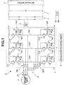
- the power conversion system 1 of this example is a system in which a three-phase AC power supplied from a three-phase AC power supply 2 is directly converted to a single-phase AC power by a power converter 3 of the embodiment of the present invention, and after the voltage of the converted AC power is stepped up or down by a transformer 4 to a suitable value, the transformed AC power is converted by a rectifier 5 to a DC power to charge a secondary battery 6.
- denoted by numeral 7 is a smoothing circuit.
- output lines (indicated by R-phase, S-phase and T-phase) to which the three-phase AC power is supplied from three-phase AC power supply 2 have at each phase a filter circuit 8 that dampens a higher harmonic wave for suppressing noise.
- Filter circuit 8 of this example comprises three filter reactors 81 respectively connected to the R, S and T phases and six filter condensers 82L and 82R each being connected between the R, S and T phases.
- the layout of filter condensers 82L and 82R (which are indicated as filter condensers 821 to 836 in Figs. 3 to 6 ) will be described hereinafter.
- the three-phase AC power is supplied to power converter 3 through filter circuit 8 and converted into the single-phase AC power.
- Power converter 3 of this example is equipped with six bidirectional switching elements 31 that are arranged in a matrix shape corresponding to the R, S and T-phases.
- bidirectional switching elements 31 that are arranged in a matrix shape corresponding to the R, S and T-phases.
- Each of bidirectional switching elements 31 of this example is constructed of an IGBT module in which IGBT (viz., Insulated Gate Bipolar Transistor), which is a semi-conductor switching element, and reflux diodes are combined and connected through an inverse-parallel connection. It is to be noted that each of bidirectional switching elements 31 is not limited to the illustrated one. That is, the switching element may have the other construction. For example, the switching element may have a construction in which two elements of reverse-blocking type IGBT are connected through an inverse-parallel connection.
- IGBT Insulated Gate Bipolar Transistor
- Each of bidirectional switching elements 31 is equipped with a snubber circuit 32 for protecting bidirectional switching element 31 from a surge voltage inevitably produced when bidirectional switching element 31 is subjected to ON/OFF operation, snubber circuit 32 including a combination of one snubber condenser and three diodes which are arranged at input and output sides of bidirectional switching element 31.
- snubber circuit 32 including a combination of one snubber condenser and three diodes which are arranged at input and output sides of bidirectional switching element 31.
- Power conversion system 1 of this example is equipped with a matrix-converter control circuit 9 for effecting ON/OFF control of bidirectional switching elements 31 of power converter.
- a value of voltage supplied from the three-phase AC power supply 2 a value of DC current that is being outputted and a target level of order current are inputted, and thereafter, based on them, respective gate signals of the bidirectional switching elements 31 are controlled to adjust the single-phase AC power directed to the transformer 4. With this, a target direct-current power is obtained.
- Transformer 4 functions to step up or down the voltage of the single-phase AC power, which has been converted by power converter 3, to a desired value.
- Rectifier 5 is equipped with four rectifying diodes to convert the adjusted single-phase AC power to a direct-current power.
- Smoothing circuit 7 is equipped with a coil and a condenser for smoothing the pulsating current contained in the rectified direct current so that the pulsating current is smoothed to show a shape much similar to a direct current.
- the three-phase AC power from three-phase AC power supply 2 is directly converted by power converter 3 to the single-phase AC power, and after the converted single-phase AC power is adjusted in voltage, the adjusted single-phase AC power is converted to the direct-current power. With this, secondary battery 6 is charged.
- the above-mentioned power conversion system 1 is one of exemplified systems to which power converter 3 of the present invention is practically applied and the present invention is not limited to application to only the above-mentioned power conversion system 1. That is, when at least one of an electric power that is to be converted and an electric power that has been converted is a polyphase AC power, the present invention is applicable to other power conversion systems.
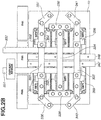
- Fig. 2 includes Figs. 2A to 2D .
- Fig. 2A is a plan view in an assembling process showing six bidirectional switching elements 31 (each being called as IGBT module) mounted on an upper surface of a heat sink 10.
- Fig. 2B is a plan view in the assembling process showing, in addition to the bidirectional switching elements, bus bars that are provided to connect terminals of bidirectional switching elements 31.
- Fig. 2C is a plan view in the assembling process of three diodes that are parts of snubber circuit 32 and filter condensers 82 of filter circuit 8, showing the left side three filter condensers mounted.
- Fig. 2D is a side view of the above-mentioned device. Since parts that constitute power converter 3 of the present invention are mutually overlapped when viewed in a plane, the following explanation on essential portions will be made with the aid of the other drawings.
- each bidirectional switching element 31 of this example is provided at an upper surface of a module package with input and output terminals and an intermediate terminal that is one of two intermediate terminals respectively provided by paired two IGBTs.
- the left side three bidirectional switching elements 311, 313 and 315 have each the input terminal at the left end, the output terminal at the right end and the intermediate terminal at the middle.
- the right side three bidirectional switching elements 312, 314 and 316 have each the input terminal at the right end, the output terminal at the left end and the intermediate terminal at the middle.
- a gate terminal of each bidirectional switching element 31 is mounted to a portion other than the module package, illustration of the gate terminal is omitted.
- the six bidirectional switching elements 311 to 316 are fixed to the upper surface of heat sink 10 through connecting means such as bolts or the like. As is seen from such drawings, the six bidirectional switching elements 311 to 316 are so arranged that paired bidirectional switching elements 311 and 312, paired bidirectional switching elements 313 and 314 and paired bidirectional switching elements 315 and 316 are placed on the left and right sides respectively with respect to a center line CL.
- the two bidirectional switching elements 311 and 312, two bidirectional switching elements 313 and 314 and two bidirectional switching elements 315 and 316 which are each paired with respect to a direction in which the three terminals (viz., input terminal, intermediate terminal and output terminal) of each bidirectional switching element 31 extend, are respectively placed on the left and right sides with respect to the center line CL.
- this arrangement will be reworded as "being arranged abreast with respect to the center line CL or output lines P and N each connecting the output terminals". It is to be noted that the arrangement is different from that shown in Fig. 5 which will be described hereinafter.
- paired bidirectional switching elements mean a pair of bidirectional switching elements that are connected to the same phase R, S or T of input line.
- paired bidirectional switching elements 311 and 312 By arranging paired bidirectional switching elements 311 and 312, paired bidirectional switching elements 313 and 314 and paired bidirectional switching elements 315 and 316 on the left and right sides respectively with respect to the center line CL as is described hereinabove, it is possible to provide a layout in which output lines P and N (bus bars 331 and 332) are drawn in one direction with the shortest distance. If the length of wiring arrangement through which a high frequency AC power is outputted is long, the arrangement is easily influenced by L-component. However, in the wiring arrangement according to the invention, influence by L-component can be suppressed. This suppression is an advantageous effect as compared with the arrange of the other example of Fig. 5 . That is, output lines P and N show nearly straight lines until reaching transformer 4.
- the terminals provided at right ends of bidirectional switching elements 311, 313 and 315 placed at the left side with respect to the center line CL are all output terminals, and the terminals provided at left ends of them are all input terminals. While, the terminals provided at left ends of bidirectional switching elements 312, 314 and 316 placed at the right side with respect to the center line CL are all output terminals, and the terminals provided at right ends of them are all input terminals.
- input lines R, S and T from three-phase AC power supply 2 to power converter 3 are branched at a position between a unit of filter reactors 81 and a unit of filter condensers 82L and 82R.
- a modification may be employed in which the branching is made at an upstream position of filter reactors 81 and the input lines R, S and T thus branched are respectively provided with filter reactors 81.
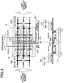
- bus bar 331 that constitutes output line P of power converter 3
- bus bar 332 that constitutes output line N of power converter 3.
- Leading ends of these bus bars 331 and 332 are connected to transformer 4.
- These bus bars 331 and 332 and after-mentioned bus bars are constructed of an electrically conductive body having good conductivity, such as copper or the like.
- the input terminals of paired bidirectional switching elements 311 and 312 placed at the left and right sides with respect to the center line CL are connected through a bus bar 333, the input terminals of bidirectional switching elements 313 and 314 are connected through a bus bar 334 and the input terminals of bidirectional switching elements 315 and 316 are connected through a bus bar 335.
- wirings corresponding to such bus bars are indicated by the same reference numerals.
- these bus bars 333 to 335 are not essential. Thus, these bus bars may be omitted.
- bus bars 333 to 335 When viewed in a plan view, these bus bars 333 to 335 are arranged to cross bus bars 331 and 332 that constitute output lines P and N. However, as is seen from the side view of Fig. 3 , bus bars 333 to 335 that connect the opposed input terminals are arranged at a position higher than bus bars 331 and 332 of output lines P and N, and thus a so-called overhead crossing is provided between them thereby to cause no mutual interference therebetween.
- filter condensers 82L and 82R each being interposed between the phases can be shared with each other. That is, between R-phase and S-phase shown in the left side of Fig. 1 , there is arranged a filter condenser 821, and between R-phase and S-phase shown in the right side of the drawing, there is arranged a filter condenser 824, and the input terminals of bidirectional switching elements 311 and 312 to which R-phase is inputted are connected through bus bar 333.
- each filter condenser can be made small in capacity resulting in that each filter condenser can be made small in size. Also in S-phase and T-phase, similar advantage is obtained from the cooperation of two filter condensers.
- filter circuit 8 has six filter condensers 821 to 826, and as is seen from Fig. 3 , the input lines placed at the left and right sides with respect to the center line CL are provided with three filter condensers respectively.
- the left side filter condenser 821 is disposed between R-phase corresponding to input terminal of bidirectional switching element 311 and S-phase.
- the left side filter condenser 822 is disposed between S-phase corresponding to the input terminal of bidirectional switching element 313 and T-phase
- the left side filter condenser 823 is disposed between T-phase corresponding to the input terminal of bidirectional switching element 315 and R-phase.
- the right side filter condenser 824 is disposed between R-phase corresponding to the input terminal of bidirectional switching element 312 and S-phase
- the right side filter condenser 825 is disposed between S-phase corresponding to the input terminal of bidirectional switching element 314 and T-phase
- the right side filter condenser 826 is disposed between T-phase corresponding to the input terminal of bidirectional switching element 316 and R-phase.
- the six filter condensers 821 to 826 in such a manner that three condensers and the other three condensers are respectively placed at the left and right sides with respect to the center line CL, the wiring distance of connecting wiring between each of filter condensers 821 to 826 and corresponding one of bidirectional switching elements 311 to 316 can be shortened.
- the six filter condensers 821 to 826 of which three filter condensers and the other three filter condensers are arranged at the left and right sides respectively are arranged outside an area where the six bidirectional switching elements 311 to 316 are placed with respect to the center line CL. Specifically, as is shown by Fig. 2D , the filter condensers are fixed to upper portions of the bus bars.
- the distance in the left-right direction between the left side bidirectional switching elements 31L and the right side bidirectional switching elements 31R can be made shortest, and thus, a distance in the left-right direction of heat sink 10 can be set to the shortest resulting in that heat sink 10 can be made small in size as compared with a heat sink shown in Fig. 4A that shows the other example.
- bus bar 331 is the output line P that connects the output terminals of bidirectional switching elements 311, 313 and 315 and leads to transformer 4
- bus bar 332 is the output line N that connects the output terminals of bidirectional switching elements 312, 314 and 316 and leads to transformer 4.
- Bus bar 333 is a bus bar for connecting the input terminals of bidirectional switching elements 311 and 312, and bus bar 333 has extension portions extending outward in the left and right directions from the respective input terminals and the extension portions are respectively connected to bus bars 336 and 337 for connecting to filter condensers 823 and 826 (the state of connection of these bus bars to filter condensers 823 and 826 is understood from Figs. 2C and 3 ).
- Bus bars 336 and 337 respectively connected to opposed ends of bus bar 333 are angled relative to a line that connects the input terminals of bidirectional switching elements 311, 313 and 315, that is a line that extends in the upward-and-downward direction in Fig. 2C .
- Bus bar 334 is a bus bar for connecting the input terminals of bidirectional switching elements 313 and 314, and bus bar 334 has extension portions extending outward in the left and right directions from the respective input terminals and the extension portions are respectively connected to bus bars 338 and 339 for connecting to filter condensers 821, 822, 824 and 825 (the state of connection of these bus bars to filter condensers 821, 822, 824 and 825 is understood from Figs. 2C and 3 ).
- Bus bars 338 and 339 respectively connected to opposed ends of bus bar 334 extend along a line that connects the input terminals of bidirectional switching elements 311, 313 and 315, that is a line that extends in the upward-and-downward direction at the upper-left portion of Fig. 2 .
- Bus bar 335 is a bus bar for connecting the input terminals of bidirectional switching elements 315 and 316, and bus bar 335 has extension portions extending outward in the left and right directions from the respective input terminals and the extension portions are respectively connected to bus bars 340 and 341 for connecting to filter condensers 823 and 826 (the state of connection of these bus bars to filter condensers 823 and 826 is understood from Figs. 2C and 3 ).
- Bus bars 340 and 341 respectively connected to opposed ends of bus bar 335 are angled relative to a line that connects the input terminals of bidirectional switching elements 311, 313 and 315, that is a line that extends in the upward-and-downward direction in Fig. 2C .
- bus bars 333, 334 and 335 are connected to the input terminals of bidirectional switching elements 311 to 316 through several bus bars 345 and 346 and positioned higher than bus bars 331 and 332 that constitute output lines P and N.
- bus bars 333 to 335 and bus bars 331 and 332 are arranged to constitute an overhead crossing therefor leaving a predetermined space therebetween, causing no mutual interference therebetween.
- filter condensers 821, 822 and 823 are positioned outside with respect to the center line CL and arranged in such a manner that centers of filter condensers 821, 822 and 823 are respectively placed at apexes of a triangle (isosceles triangle or equilateral triangle is preferable) of which one apex is directed outward.
- a triangle isosceles triangle or equilateral triangle is preferable
- the wiring length between the condensers can be made shortest and thus, power converter 3 can be made small in size and synchronization between the condensers can be assured.
- bus bars 336 and 340 or bus bars 337 and 341, which are connected to filter condenser 823 or 826 respectively, are angled to each other to shorten the distance therebetween.
- the distances from filter condenser 823 or 826 to respective bus bars 333 and 335 can be much shortened, and thus, equalization of wiring lengths between the condensers is assured.
- filter condensers 821, 822, 824 and 825 can be actually mounted without considering the sizes thereof, and thus, the degree of freedom in designing of the condensers can be increased.
- Filter condenser 821 disposed between R-phase and S-phase is mounted on an upper surface of bus bar 342 and filter condenser 822 disposed between S-phase and T-phase is mounted on an upper surface of bus bar 343.
- These two bus bars 342 and 343 are connected while being angled relative to a line that connects the input terminals of bidirectional switching elements 311, 313 and 315, that is, a line that extends in the upward-and-downward direction in Fig. 2C .
- bus bars 342 and 343 are connected to bus bars 333, 342 and 335 while straddling a line that connects the input terminals of bidirectional switching elements 311, 313 and 315, that is a line that extends in the upward-and-downward direction in Fig. 2C .
- filter condensers 824 and 825 mounted at the right side of the center line CL are symmetrically arranged relative to filter condensers 821 and 822 with respect to the center line CL.
- bus bars 342 and 343 By arranging bus bars 342 and 343 in such a manner that these bus bars are angled relative to the line that connects the input terminals of bidirectional switching elements 311, 313 and 315, synchronization among filter condensers 821, 822 and 823 is assured because the wiring distance between the filter condensers can be finely equalized with the wiring distance of filter condenser 823 disposed between R-phase and T-phase.
- bus bars 342 and 343 in such a manner that these bus bars straggle the line that connects the input terminals of bidirectional switching elements 311, 313 and 315, the connecting distance between filter condensers 821 and 822 and bus bars 333, 334 and 335 can be shortened, and thus, power converter 3 can be made small in size. Furthermore, by arranging filter condensers 821 to 826 on upper surfaces of the bus bars, that is, by arranging filter condensers 821 to 826 at an opposite side of bidirectional switching elements 311 to 316 with respect to the bus bars, the degree of freedom in designing layout of filter condensers 821 to 826 is increased.
- Filter condenser 823 disposed between R-phase and T-phase is mounted on an upper surface of bus bar 344 disposed between bus bars 336 and 340, and bus bar 344 is arranged to extend in parallel with a line that connects the input terminals of bidirectional switching elements 311, 313 and 315.
- snubber circuit 321 for example, of bidirectional switching element 311 has one terminal connected to the input terminal of bidirectional switching terminal 311, another terminal connected to the intermediate terminal of bidirectional switching element 311 and still another terminal connected to the output terminal of bidirectional switching element 311.
- the three diodes are fixed and connected to brackets 351 to 356 which are each constructed of an electrically conductive body connected to an intermediate terminal between each bidirectional switching element 31L and corresponding bidirectional switching element 31R.
- bracket 355 is shown.
- a relatively large-sized electrolytic condenser is used as the snubber condenser, and the relatively large-sized electrolytic condenser is used as a common snubber condenser 327 (see Fig. 3 ) for the six snubber circuits 321 to 326.
- the bus bars 347 and 348 are provided for connecting snubber condenser 327 and the three diodes, there are provided bus bars 347 and 348 that are placed between bus bars 331 and 332 and extend in the same direction as these bus bars 331 and 332, the bus bars 331 and 332 constituting the output lines P and N.
- bus bars 347 and 348 connected to snubber condenser 327 are fixed to a position that is higher than bus bars 331 and 332 that constitute the output lines P and N but lower than bus bars 333, 334 and 335. It is to be noted that these two bus bars 347 and 348 are supported on heat sink 10 or a base (not shown) other than the heat sink. For preventing a short-circuit with bus bars 333, 334 and 335, outer surfaces of bus bars 347 and 348 may be coated with an insulating material.
- bus bars 347 and 348 with respect to bus bars 331 and 332 that constitute output lines P and N and snubber condenser 327 is as follows. That is, by arranging bus bars 347 and 348 between bus bars 331 and 332, both the wiring distance to output lines P and N and the wiring distance to snubber condenser 327 can be shortened. Furthermore, by arranging bus bars 347 and 348 higher than bus bars 331 and 332, it is possible to shorten the distance from the diodes of each of snubber circuits 321 to 326.
- the present invention has modifications and embodiments other than the above-mentioned embodiment. In the following, modifications of the invention will be described. The present invention is not limited to the above-mentioned embodiment and the following embodiments. In the following, parts identical to those described in the above-mentioned embodiment are indicated by the same reference numerals and explanation on the same parts will be suitably omitted.
- the three left side filter condensers 82L and the three right side filter condensers 82R are arranged outside an area of bidirectional switching elements 311, 313 and 315 and an area of bidirectional switching elements 312, 314 and 316 respectively with respect to the center line CL.
- the three left side filter condensers and the three right side condensers may be arranged between an area of the left side bidirectional switching elements 311, 313 and 315 and an area of the right side bidirectional switching elements 312, 314 and 316 with respect to the center line CL.
- bidirectional switching elements 311 to 316 are so arranged that bidirectional switching elements 311, 313 and 315 and bidirectional switching elements 312, 314 and 316 are arranged at the left and right sides respectively with respect to the center line CL.
- bidirectional switching elements 311, 313 and 315 and bidirectional switching elements 312, 314 and 316 may be arranged along the center line CL.
- the six bidirectional switching elements 311 to 316 are so arranged that bidirectional switching elements 311, 313 and 315 and bidirectional switching elements 312, 314 and 316 are arranged at the left and right sides respectively with respect to the center line CL and the input and output terminals of the left side bidirectional switching elements and the input and output terminals of the right side bidirectional switching elements are arranged in line symmetry with respect to the center line CL.
- bidirectional switching elements 311, 313 and 315 and bidirectional switching elements 312, 314 and 316 are arranged at the left and right sides respectively with respect to the center line CL and the input and output terminals of the left side bidirectional switching elements and the input and output terminals of the right side bidirectional switching elements are arranged in line symmetry with respect to the center line CL.
- bidirectional switching elements 311, 313 and 315 and bidirectional switching elements 312, 314 and 316 are arranged at the left and right sides with respect to the center line CL and the input and output terminals of the left side bidirectional switching elements and the input and output terminals of the right side bidirectional switching elements are arranged in the same manner.
- input lines R, S and T of the dual system are connected to the input terminals of the left and right side bidirectional switching elements while extending in the same direction (in the direction from left to right in the illustrated example).
- filter condensers 821 to 826 are arranged between the phases while keeping one-to-one relation to the six bidirectional switching elements 311 to 316.
- Fig. 7 an arrangement may be employed in which filter condensers 821 to 826 are arranged between the phases in such a manner that several (two in the illustrated example) of the filter condensers 821 to 826 are connected to each of the six bidirectional switching elements 311 to 316.
- the filter condensers may be arranged at the center of power converter 3 as is shown in Fig. 8 or outside power converter 3 as is shown in Fig. 9 .
- Fig. 8 when the filter condensers are arranged at the center of power converter 3, empty spaces are usable, so that the size of power converter 3 can be made as small as possible.
- the above-mentioned bidirectional switching elements 311, 313 and 315 correspond to first switching elements in Claims
- the above-mentioned bidirectional switching elements 312, 314 and 316 correspond to second switching elements in Claims
- the above-mentioned power converter 3 corresponds to a converter circuit in Claims
- the above-mentioned filter condensers 821 to 826 and 831 to 836 correspond to condensers in Claims
- the above-mentioned bus bars 331 and 332 correspond to output lines in Claims.
Landscapes
- Engineering & Computer Science (AREA)
- Power Engineering (AREA)
- Microelectronics & Electronic Packaging (AREA)
- Ac-Ac Conversion (AREA)
- Power Conversion In General (AREA)
- Inverter Devices (AREA)
- Dc-Dc Converters (AREA)
Claims (7)
- Convertisseur de puissance (1) adapté pour convertir directement une puissance en courant alternatif polyphasée en une puissance en courant alternatif, le convertisseur de puissance (1) comprenant :un circuit convertisseur (3) comportant une pluralité de premiers éléments de commutation (311, 313, 315) qui sont adaptés pour être reliés à chaque phase de la puissance en courant alternatif polyphasée pour permettre la commutation afin d'activer le transport de courant de manière bidirectionnelle et une pluralité de deuxièmes éléments de commutation (312, 314, 316) qui sont adaptés pour être reliés à chaque phase de la puissance en courant alternatif polyphasée pour permettre la commutation afin d'activer le transport de courant de manière bidirectionnelle ; etune pluralité de condensateurs (821, ..., 826, 831, ..., 836) reliés au circuit convertisseur,dans lequel au moins l'un des condensateurs (821, ..., 826, 831, ..., 836) est disposé entre des phases de la puissance en courant alternatif polyphasée appliquée aux premiers éléments de commutation (311, 313, 315) et entre des phases de la puissance en courant alternatif polyphasée appliquée aux deuxièmes éléments de commutation (312, 314, 316) etcaractérisé en ce qu'un agencement spatial est fourni par :un agencement dans lequel des bornes de la pluralité de premiers éléments de commutation (311, 313, 315) sont agencées en ligne et les bornes de la pluralité de deuxièmes éléments de commutation (312, 314, 316) sont agencées en ligne ; etun agencement dans lequel certains condensateurs (821, 822, 824, 825, 831, 832, 834, 835) de la pluralité de condensateurs (821, ..., 826, 831, ..., 836) sont montés sur des barres omnibus inclinées (342, 343), qui sont agencées pour être inclinées par rapport aux lignes que forment les bornes.
- Convertisseur de puissance (1) tel que revendiqué dans la revendication 1, dans lequel des bornes de connexion prévues au niveau des deux extrémités de chacun des certains condensateurs (821, 822, 824, 825, 831, 832, 834, 835) sont agencées pour mettre entre elles la ligne qui relie la pluralité de bornes agencées en ligne.
- Convertisseur de puissance (1) tel que revendiqué dans la revendication 1, dans lequel les autres condensateurs (821, 822, 824, 825, 831, 832, 834, 835) de la pluralité de condensateurs (821, ..., 826, 831, ..., 836) sont agencés en parallèle avec la direction d'agencement des bornes.
- Convertisseur de puissance (1) tel que revendiqué dans la revendication 3, dans lequel des câblages pour relier les autres condensateurs (821, 822, 824, 825, 831, 832, 834, 835) aux phases sont agencés pour être inclinés par rapport à la direction d'agencement des bornes.
- Convertisseur de puissance (1) tel que revendiqué dans la revendication 1, comprenant en outre :une première barre omnibus (331, 332) qui s'étend dans une direction perpendiculaire à la direction d'agencement des bornes, la première barre omnibus (331, 332) étant reliée à au moins l'un des premiers éléments de commutation (311, 313, 315) et des deuxièmes éléments de commutation (312, 314, 316) qui correspondent à l'une des phases (P, N) ;une deuxième barre omnibus (333, 334, 335) qui s'étend dans la direction d'agencement des bornes à partir d'une extrémité de la première barre omnibus (331, 332) et est reliée à une borne de l'un parmi les certains condensateurs (821, ..., 826, 831, ..., 836).
- Convertisseur de puissance (1) tel que revendiqué dans la revendication 1, comprenant en outre une pluralité de barres omnibus droites qui correspondent respectivement aux phases et sont agencées pour s'étendre en parallèle les unes avec les autres, dans lequel les certains condensateurs (821, 822, 824, 825, 831, 832, 834, 835) sont montés sur des barres omnibus inclinées, qui sont agencées pour être inclinées par rapport aux barres omnibus droites.
- Convertisseur de puissance (1) tel que revendiqué dans la revendication 6, dans lequel chacune des barres omnibus droites relie des bornes d'entrée respectives des premiers éléments de commutation (311, 313, 315) et deuxièmes éléments de commutation (311, 313, 315) qui correspondent à la même phase.
Applications Claiming Priority (2)
| Application Number | Priority Date | Filing Date | Title |
|---|---|---|---|
| JP2011122842A JP5377574B2 (ja) | 2011-05-31 | 2011-05-31 | 電力変換装置 |
| PCT/JP2012/061658 WO2012165103A1 (fr) | 2011-05-31 | 2012-05-07 | Dispositif de conversion de puissance |
Publications (3)
| Publication Number | Publication Date |
|---|---|
| EP2717452A1 EP2717452A1 (fr) | 2014-04-09 |
| EP2717452A4 EP2717452A4 (fr) | 2015-11-25 |
| EP2717452B1 true EP2717452B1 (fr) | 2021-03-10 |
Family
ID=47258967
Family Applications (1)
| Application Number | Title | Priority Date | Filing Date |
|---|---|---|---|
| EP12792428.0A Active EP2717452B1 (fr) | 2011-05-31 | 2012-05-07 | Dispositif de conversion de puissance |
Country Status (9)
| Country | Link |
|---|---|
| US (1) | US9490721B2 (fr) |
| EP (1) | EP2717452B1 (fr) |
| JP (1) | JP5377574B2 (fr) |
| CN (1) | CN103650317B (fr) |
| BR (1) | BR112013030560B1 (fr) |
| MX (1) | MX2013013987A (fr) |
| MY (1) | MY158683A (fr) |
| RU (1) | RU2557561C1 (fr) |
| WO (1) | WO2012165103A1 (fr) |
Families Citing this family (7)
| Publication number | Priority date | Publication date | Assignee | Title |
|---|---|---|---|---|
| JP5377575B2 (ja) * | 2011-05-31 | 2013-12-25 | 日産自動車株式会社 | 電力変換装置 |
| JP5437312B2 (ja) | 2011-05-31 | 2014-03-12 | 日産自動車株式会社 | 電力変換装置 |
| EP2765699B1 (fr) * | 2011-10-07 | 2017-03-29 | Nissan Motor Co., Ltd | Convertisseur de puissance |
| JP5420122B2 (ja) * | 2011-10-07 | 2014-02-19 | 日産自動車株式会社 | 電力変換装置 |
| JP6477893B2 (ja) * | 2015-08-28 | 2019-03-06 | 株式会社村田製作所 | Dc−dcコンバータ |
| RU176542U1 (ru) * | 2017-02-07 | 2018-01-23 | Открытое акционерное общество "Электровыпрямитель" | Устройство для формирования импульсов управления диодно-тиристорным мостом |
| JP6488421B1 (ja) * | 2018-09-12 | 2019-03-20 | 高周波熱錬株式会社 | スナバ回路及びパワー半導体モジュール並びに誘導加熱用電源装置 |
Citations (1)
| Publication number | Priority date | Publication date | Assignee | Title |
|---|---|---|---|---|
| US20080315819A1 (en) * | 2004-09-29 | 2008-12-25 | Kabushiki Kaisha Yaskawa Denki | Parallel Multiplex Matrix Converter |
Family Cites Families (47)
| Publication number | Priority date | Publication date | Assignee | Title |
|---|---|---|---|---|
| WO1980001742A1 (fr) * | 1979-02-08 | 1980-08-21 | Tatsuta Densen Kk | Detecteur de desequilibre entre phases pour un circuit de charge en courant alternatif |
| US4468725A (en) * | 1982-06-18 | 1984-08-28 | Texas Instruments Incorporated | Direct AC converter for converting a balanced AC polyphase input to an output voltage |
| US4833584A (en) * | 1987-10-16 | 1989-05-23 | Wisconsin Alumni Research Foundation | Quasi-resonant current mode static power conversion method and apparatus |
| JP2704519B2 (ja) * | 1988-03-09 | 1998-01-26 | オリジン電気株式会社 | 直流電源装置 |
| JPH0628292B2 (ja) | 1988-11-11 | 1994-04-13 | 富士電機株式会社 | 逆阻止形トランジスタモジュール |
| US5010471A (en) * | 1989-06-26 | 1991-04-23 | Robert F. Frijouf | Three-phase AC-to-AC series resonant power converter with reduced number of switches |
| JP2719012B2 (ja) * | 1989-10-31 | 1998-02-25 | 三菱電機株式会社 | インバータ装置 |
| GB2242580B (en) | 1990-03-30 | 1994-06-15 | Mitsubishi Electric Corp | Inverter unit with improved bus-plate configuration |
| US5287260A (en) * | 1991-10-21 | 1994-02-15 | Kabushiki Kaisha Toshiba | GTO rectifier and inverter |
| JP2896454B2 (ja) * | 1992-11-25 | 1999-05-31 | 株式会社日立製作所 | インバータ装置 |
| JP3195105B2 (ja) * | 1993-02-26 | 2001-08-06 | 株式会社東芝 | 多相入力用直流電源回路 |
| JPH06261556A (ja) | 1993-03-04 | 1994-09-16 | Toshiba Corp | 半導体スイッチ装置 |
| US5517063A (en) | 1994-06-10 | 1996-05-14 | Westinghouse Electric Corp. | Three phase power bridge assembly |
| SE9500761D0 (sv) | 1995-03-02 | 1995-03-02 | Abb Research Ltd | Skyddskrets för seriekopplade krafthalvledare |
| US6266258B1 (en) | 1995-09-29 | 2001-07-24 | Rockwell Technologies, Llc | Power substrate element topology |
| FI110370B (fi) | 1998-07-31 | 2002-12-31 | Lexel Finland Ab Oy | Järjestely elektronisen tehonsäätimen radiohäiriöiden eliminoimiseksi |
| JP2001045772A (ja) | 1999-08-03 | 2001-02-16 | Yaskawa Electric Corp | 3レベルインバータまたはpwmサイクロコンバータ |
| DE10014641C2 (de) | 2000-03-24 | 2002-03-07 | Siemens Ag | Schaltungsanordnung mit einem bidirektionalen Leistungsschalter in Common Kollektor Mode und mit einer aktiven Überspannungsschutzvorrichtung |
| DE10037970A1 (de) | 2000-08-03 | 2002-03-07 | Siemens Ag | Niederinduktive Verschienung für einen Matrixumrichter |
| JP3793407B2 (ja) | 2000-09-19 | 2006-07-05 | 株式会社日立製作所 | 電力変換装置 |
| JP4501145B2 (ja) * | 2001-02-23 | 2010-07-14 | Tdkラムダ株式会社 | 三相ノイズフィルタ |
| JP4337443B2 (ja) * | 2003-08-12 | 2009-09-30 | 株式会社日立製作所 | マトリクスコンバータシステム |
| JP4293000B2 (ja) | 2004-01-29 | 2009-07-08 | 株式会社日立製作所 | 電力変換装置 |
| JP4296960B2 (ja) * | 2004-02-20 | 2009-07-15 | 株式会社日立製作所 | 電力変換装置 |
| JP4581777B2 (ja) | 2005-03-24 | 2010-11-17 | トヨタ自動車株式会社 | パワーモジュール |
| JP4765017B2 (ja) * | 2005-05-25 | 2011-09-07 | 富士電機株式会社 | Ac−ac電力変換装置 |
| JP2009507462A (ja) * | 2005-09-09 | 2009-02-19 | シーメンス アクチエンゲゼルシヤフト | 電気エネルギー伝送のための装置 |
| US7869193B2 (en) | 2006-02-17 | 2011-01-11 | Kabushiki Kaisha Yaskawa Denki | Power conversion apparatus |
| JP4793096B2 (ja) * | 2006-05-24 | 2011-10-12 | 株式会社明電舎 | 高圧交流直接電力変換装置 |
| CN104300771B (zh) * | 2006-06-06 | 2018-10-30 | 威廉·亚历山大 | 通用功率变换器 |
| US8008805B2 (en) | 2006-12-07 | 2011-08-30 | Nissan Motor Co., Ltd. | Power conversion apparatus and motor drive system |
| JP4720756B2 (ja) | 2007-02-22 | 2011-07-13 | トヨタ自動車株式会社 | 半導体電力変換装置およびその製造方法 |
| US7573732B2 (en) | 2007-05-25 | 2009-08-11 | General Electric Company | Protective circuit and method for multi-level converter |
| US20090052134A1 (en) | 2007-08-22 | 2009-02-26 | Casteel Jordan B | Liquid-cooled grounded heatsink for diode rectifier system |
| EP2099119B1 (fr) | 2008-03-04 | 2014-11-19 | Kabushiki Kaisha Toyota Jidoshokki | Appareil convertisseur de puissance |
| JP4640423B2 (ja) | 2008-03-04 | 2011-03-02 | 株式会社豊田自動織機 | 電力変換装置 |
| CN101540580B (zh) * | 2008-03-18 | 2012-03-14 | 新能动力(北京)电气科技有限公司 | 一种电能回馈装置 |
| WO2009144987A1 (fr) * | 2008-05-30 | 2009-12-03 | 株式会社安川電機 | Dispositif de commande pour convertisseur matriciel et son procédé de génération de tension de sortie |
| JP5586872B2 (ja) * | 2009-05-07 | 2014-09-10 | 電気興業株式会社 | 三相単相直接電力変換器回路 |
| EP2296156A1 (fr) | 2009-08-13 | 2011-03-16 | ABB Research Ltd | Capacité composite et son utilisation |
| US8411474B2 (en) | 2010-04-30 | 2013-04-02 | General Electric Company | System and method for protection of a multilevel converter |
| JP5590448B2 (ja) | 2010-07-20 | 2014-09-17 | 株式会社安川電機 | マトリクスコンバータ |
| JP2012054449A (ja) | 2010-09-02 | 2012-03-15 | Aisin Aw Co Ltd | 電気的接続装置 |
| EP2512023A3 (fr) | 2011-04-14 | 2017-06-28 | General Electric Technology GmbH | Agencement de convertisseur de puissance et procédé pour exploiter un agencement de convertisseur de puissance |
| JP5420122B2 (ja) | 2011-10-07 | 2014-02-19 | 日産自動車株式会社 | 電力変換装置 |
| EP2765699B1 (fr) | 2011-10-07 | 2017-03-29 | Nissan Motor Co., Ltd | Convertisseur de puissance |
| RU2014122084A (ru) * | 2011-12-19 | 2016-02-10 | ЗедБиБи ЭНЕРДЖИ КОРОПОРЕЙШН | Система и способ управления многофазной машиной переменного тока при низкой скорости вращения |
-
2011
- 2011-05-31 JP JP2011122842A patent/JP5377574B2/ja active Active
-
2012
- 2012-05-07 MY MYPI2013004131A patent/MY158683A/en unknown
- 2012-05-07 MX MX2013013987A patent/MX2013013987A/es active IP Right Grant
- 2012-05-07 RU RU2013158883/07A patent/RU2557561C1/ru active
- 2012-05-07 WO PCT/JP2012/061658 patent/WO2012165103A1/fr active Application Filing
- 2012-05-07 US US14/122,268 patent/US9490721B2/en active Active
- 2012-05-07 CN CN201280025374.8A patent/CN103650317B/zh active Active
- 2012-05-07 EP EP12792428.0A patent/EP2717452B1/fr active Active
- 2012-05-07 BR BR112013030560-6A patent/BR112013030560B1/pt active IP Right Grant
Patent Citations (1)
| Publication number | Priority date | Publication date | Assignee | Title |
|---|---|---|---|---|
| US20080315819A1 (en) * | 2004-09-29 | 2008-12-25 | Kabushiki Kaisha Yaskawa Denki | Parallel Multiplex Matrix Converter |
Also Published As
| Publication number | Publication date |
|---|---|
| JP5377574B2 (ja) | 2013-12-25 |
| RU2013158883A (ru) | 2015-07-10 |
| CN103650317B (zh) | 2016-06-22 |
| MX2013013987A (es) | 2014-05-27 |
| CN103650317A (zh) | 2014-03-19 |
| WO2012165103A1 (fr) | 2012-12-06 |
| US20140085950A1 (en) | 2014-03-27 |
| BR112013030560A2 (pt) | 2016-09-27 |
| US9490721B2 (en) | 2016-11-08 |
| EP2717452A4 (fr) | 2015-11-25 |
| BR112013030560B1 (pt) | 2020-11-03 |
| EP2717452A1 (fr) | 2014-04-09 |
| MY158683A (en) | 2016-10-31 |
| RU2557561C1 (ru) | 2015-07-27 |
| JP2012253856A (ja) | 2012-12-20 |
Similar Documents
| Publication | Publication Date | Title |
|---|---|---|
| EP2717453B1 (fr) | Dispositif de conversion de puissance | |
| EP2717454B1 (fr) | Dispositif de conversion de puissance | |
| EP2717452B1 (fr) | Dispositif de conversion de puissance | |
| EP2717456B1 (fr) | Dispositif de conversion de puissance | |
| EP2717457B1 (fr) | Dispositif de conversion de puissance | |
| EP2717455B1 (fr) | Dispositif de conversion de puissance | |
| JP5476510B2 (ja) | 電力変換装置 | |
| WO2013051476A1 (fr) | Convertisseur de puissance |
Legal Events
| Date | Code | Title | Description |
|---|---|---|---|
| PUAI | Public reference made under article 153(3) epc to a published international application that has entered the european phase |
Free format text: ORIGINAL CODE: 0009012 |
|
| 17P | Request for examination filed |
Effective date: 20131126 |
|
| AK | Designated contracting states |
Kind code of ref document: A1 Designated state(s): AL AT BE BG CH CY CZ DE DK EE ES FI FR GB GR HR HU IE IS IT LI LT LU LV MC MK MT NL NO PL PT RO RS SE SI SK SM TR |
|
| DAX | Request for extension of the european patent (deleted) | ||
| RA4 | Supplementary search report drawn up and despatched (corrected) |
Effective date: 20151027 |
|
| RIC1 | Information provided on ipc code assigned before grant |
Ipc: H02M 5/293 20060101AFI20151021BHEP Ipc: H05K 7/14 20060101ALI20151021BHEP Ipc: H02M 7/00 20060101ALI20151021BHEP Ipc: H02M 1/12 20060101ALI20151021BHEP |
|
| STAA | Information on the status of an ep patent application or granted ep patent |
Free format text: STATUS: EXAMINATION IS IN PROGRESS |
|
| 17Q | First examination report despatched |
Effective date: 20170301 |
|
| GRAP | Despatch of communication of intention to grant a patent |
Free format text: ORIGINAL CODE: EPIDOSNIGR1 |
|
| STAA | Information on the status of an ep patent application or granted ep patent |
Free format text: STATUS: GRANT OF PATENT IS INTENDED |
|
| INTG | Intention to grant announced |
Effective date: 20201223 |
|
| GRAS | Grant fee paid |
Free format text: ORIGINAL CODE: EPIDOSNIGR3 |
|
| GRAA | (expected) grant |
Free format text: ORIGINAL CODE: 0009210 |
|
| STAA | Information on the status of an ep patent application or granted ep patent |
Free format text: STATUS: THE PATENT HAS BEEN GRANTED |
|
| AK | Designated contracting states |
Kind code of ref document: B1 Designated state(s): AL AT BE BG CH CY CZ DE DK EE ES FI FR GB GR HR HU IE IS IT LI LT LU LV MC MK MT NL NO PL PT RO RS SE SI SK SM TR |
|
| REG | Reference to a national code |
Ref country code: GB Ref legal event code: FG4D |
|
| REG | Reference to a national code |
Ref country code: AT Ref legal event code: REF Ref document number: 1370931 Country of ref document: AT Kind code of ref document: T Effective date: 20210315 Ref country code: CH Ref legal event code: EP |
|
| REG | Reference to a national code |
Ref country code: IE Ref legal event code: FG4D |
|
| REG | Reference to a national code |
Ref country code: DE Ref legal event code: R096 Ref document number: 602012074736 Country of ref document: DE |
|
| REG | Reference to a national code |
Ref country code: LT Ref legal event code: MG9D |
|
| PG25 | Lapsed in a contracting state [announced via postgrant information from national office to epo] |
Ref country code: LT Free format text: LAPSE BECAUSE OF FAILURE TO SUBMIT A TRANSLATION OF THE DESCRIPTION OR TO PAY THE FEE WITHIN THE PRESCRIBED TIME-LIMIT Effective date: 20210310 Ref country code: FI Free format text: LAPSE BECAUSE OF FAILURE TO SUBMIT A TRANSLATION OF THE DESCRIPTION OR TO PAY THE FEE WITHIN THE PRESCRIBED TIME-LIMIT Effective date: 20210310 Ref country code: HR Free format text: LAPSE BECAUSE OF FAILURE TO SUBMIT A TRANSLATION OF THE DESCRIPTION OR TO PAY THE FEE WITHIN THE PRESCRIBED TIME-LIMIT Effective date: 20210310 Ref country code: GR Free format text: LAPSE BECAUSE OF FAILURE TO SUBMIT A TRANSLATION OF THE DESCRIPTION OR TO PAY THE FEE WITHIN THE PRESCRIBED TIME-LIMIT Effective date: 20210611 Ref country code: NO Free format text: LAPSE BECAUSE OF FAILURE TO SUBMIT A TRANSLATION OF THE DESCRIPTION OR TO PAY THE FEE WITHIN THE PRESCRIBED TIME-LIMIT Effective date: 20210610 Ref country code: BG Free format text: LAPSE BECAUSE OF FAILURE TO SUBMIT A TRANSLATION OF THE DESCRIPTION OR TO PAY THE FEE WITHIN THE PRESCRIBED TIME-LIMIT Effective date: 20210610 |
|
| REG | Reference to a national code |
Ref country code: AT Ref legal event code: MK05 Ref document number: 1370931 Country of ref document: AT Kind code of ref document: T Effective date: 20210310 |
|
| REG | Reference to a national code |
Ref country code: NL Ref legal event code: MP Effective date: 20210310 |
|
| PG25 | Lapsed in a contracting state [announced via postgrant information from national office to epo] |
Ref country code: SE Free format text: LAPSE BECAUSE OF FAILURE TO SUBMIT A TRANSLATION OF THE DESCRIPTION OR TO PAY THE FEE WITHIN THE PRESCRIBED TIME-LIMIT Effective date: 20210310 Ref country code: LV Free format text: LAPSE BECAUSE OF FAILURE TO SUBMIT A TRANSLATION OF THE DESCRIPTION OR TO PAY THE FEE WITHIN THE PRESCRIBED TIME-LIMIT Effective date: 20210310 Ref country code: RS Free format text: LAPSE BECAUSE OF FAILURE TO SUBMIT A TRANSLATION OF THE DESCRIPTION OR TO PAY THE FEE WITHIN THE PRESCRIBED TIME-LIMIT Effective date: 20210310 |
|
| PG25 | Lapsed in a contracting state [announced via postgrant information from national office to epo] |
Ref country code: NL Free format text: LAPSE BECAUSE OF FAILURE TO SUBMIT A TRANSLATION OF THE DESCRIPTION OR TO PAY THE FEE WITHIN THE PRESCRIBED TIME-LIMIT Effective date: 20210310 |
|
| PG25 | Lapsed in a contracting state [announced via postgrant information from national office to epo] |
Ref country code: EE Free format text: LAPSE BECAUSE OF FAILURE TO SUBMIT A TRANSLATION OF THE DESCRIPTION OR TO PAY THE FEE WITHIN THE PRESCRIBED TIME-LIMIT Effective date: 20210310 Ref country code: CZ Free format text: LAPSE BECAUSE OF FAILURE TO SUBMIT A TRANSLATION OF THE DESCRIPTION OR TO PAY THE FEE WITHIN THE PRESCRIBED TIME-LIMIT Effective date: 20210310 Ref country code: SM Free format text: LAPSE BECAUSE OF FAILURE TO SUBMIT A TRANSLATION OF THE DESCRIPTION OR TO PAY THE FEE WITHIN THE PRESCRIBED TIME-LIMIT Effective date: 20210310 Ref country code: AT Free format text: LAPSE BECAUSE OF FAILURE TO SUBMIT A TRANSLATION OF THE DESCRIPTION OR TO PAY THE FEE WITHIN THE PRESCRIBED TIME-LIMIT Effective date: 20210310 |
|
| PG25 | Lapsed in a contracting state [announced via postgrant information from national office to epo] |
Ref country code: IS Free format text: LAPSE BECAUSE OF FAILURE TO SUBMIT A TRANSLATION OF THE DESCRIPTION OR TO PAY THE FEE WITHIN THE PRESCRIBED TIME-LIMIT Effective date: 20210710 Ref country code: RO Free format text: LAPSE BECAUSE OF FAILURE TO SUBMIT A TRANSLATION OF THE DESCRIPTION OR TO PAY THE FEE WITHIN THE PRESCRIBED TIME-LIMIT Effective date: 20210310 Ref country code: ES Free format text: LAPSE BECAUSE OF FAILURE TO SUBMIT A TRANSLATION OF THE DESCRIPTION OR TO PAY THE FEE WITHIN THE PRESCRIBED TIME-LIMIT Effective date: 20210310 Ref country code: PT Free format text: LAPSE BECAUSE OF FAILURE TO SUBMIT A TRANSLATION OF THE DESCRIPTION OR TO PAY THE FEE WITHIN THE PRESCRIBED TIME-LIMIT Effective date: 20210712 Ref country code: PL Free format text: LAPSE BECAUSE OF FAILURE TO SUBMIT A TRANSLATION OF THE DESCRIPTION OR TO PAY THE FEE WITHIN THE PRESCRIBED TIME-LIMIT Effective date: 20210310 Ref country code: SK Free format text: LAPSE BECAUSE OF FAILURE TO SUBMIT A TRANSLATION OF THE DESCRIPTION OR TO PAY THE FEE WITHIN THE PRESCRIBED TIME-LIMIT Effective date: 20210310 |
|
| REG | Reference to a national code |
Ref country code: DE Ref legal event code: R097 Ref document number: 602012074736 Country of ref document: DE |
|
| REG | Reference to a national code |
Ref country code: CH Ref legal event code: PL |
|
| PLBE | No opposition filed within time limit |
Free format text: ORIGINAL CODE: 0009261 |
|
| STAA | Information on the status of an ep patent application or granted ep patent |
Free format text: STATUS: NO OPPOSITION FILED WITHIN TIME LIMIT |
|
| PG25 | Lapsed in a contracting state [announced via postgrant information from national office to epo] |
Ref country code: DK Free format text: LAPSE BECAUSE OF FAILURE TO SUBMIT A TRANSLATION OF THE DESCRIPTION OR TO PAY THE FEE WITHIN THE PRESCRIBED TIME-LIMIT Effective date: 20210310 Ref country code: AL Free format text: LAPSE BECAUSE OF FAILURE TO SUBMIT A TRANSLATION OF THE DESCRIPTION OR TO PAY THE FEE WITHIN THE PRESCRIBED TIME-LIMIT Effective date: 20210310 Ref country code: CH Free format text: LAPSE BECAUSE OF NON-PAYMENT OF DUE FEES Effective date: 20210531 Ref country code: LI Free format text: LAPSE BECAUSE OF NON-PAYMENT OF DUE FEES Effective date: 20210531 Ref country code: LU Free format text: LAPSE BECAUSE OF NON-PAYMENT OF DUE FEES Effective date: 20210507 Ref country code: MC Free format text: LAPSE BECAUSE OF FAILURE TO SUBMIT A TRANSLATION OF THE DESCRIPTION OR TO PAY THE FEE WITHIN THE PRESCRIBED TIME-LIMIT Effective date: 20210310 |
|
| REG | Reference to a national code |
Ref country code: BE Ref legal event code: MM Effective date: 20210531 |
|
| 26N | No opposition filed |
Effective date: 20211213 |
|
| PG25 | Lapsed in a contracting state [announced via postgrant information from national office to epo] |
Ref country code: SI Free format text: LAPSE BECAUSE OF FAILURE TO SUBMIT A TRANSLATION OF THE DESCRIPTION OR TO PAY THE FEE WITHIN THE PRESCRIBED TIME-LIMIT Effective date: 20210310 |
|
| PG25 | Lapsed in a contracting state [announced via postgrant information from national office to epo] |
Ref country code: IT Free format text: LAPSE BECAUSE OF FAILURE TO SUBMIT A TRANSLATION OF THE DESCRIPTION OR TO PAY THE FEE WITHIN THE PRESCRIBED TIME-LIMIT Effective date: 20210310 Ref country code: IE Free format text: LAPSE BECAUSE OF NON-PAYMENT OF DUE FEES Effective date: 20210507 |
|
| PG25 | Lapsed in a contracting state [announced via postgrant information from national office to epo] |
Ref country code: IS Free format text: LAPSE BECAUSE OF FAILURE TO SUBMIT A TRANSLATION OF THE DESCRIPTION OR TO PAY THE FEE WITHIN THE PRESCRIBED TIME-LIMIT Effective date: 20210710 |
|
| PG25 | Lapsed in a contracting state [announced via postgrant information from national office to epo] |
Ref country code: BE Free format text: LAPSE BECAUSE OF NON-PAYMENT OF DUE FEES Effective date: 20210531 |
|
| PG25 | Lapsed in a contracting state [announced via postgrant information from national office to epo] |
Ref country code: HU Free format text: LAPSE BECAUSE OF FAILURE TO SUBMIT A TRANSLATION OF THE DESCRIPTION OR TO PAY THE FEE WITHIN THE PRESCRIBED TIME-LIMIT; INVALID AB INITIO Effective date: 20120507 Ref country code: CY Free format text: LAPSE BECAUSE OF FAILURE TO SUBMIT A TRANSLATION OF THE DESCRIPTION OR TO PAY THE FEE WITHIN THE PRESCRIBED TIME-LIMIT Effective date: 20210310 |
|
| PG25 | Lapsed in a contracting state [announced via postgrant information from national office to epo] |
Ref country code: MK Free format text: LAPSE BECAUSE OF FAILURE TO SUBMIT A TRANSLATION OF THE DESCRIPTION OR TO PAY THE FEE WITHIN THE PRESCRIBED TIME-LIMIT Effective date: 20210310 |
|
| PG25 | Lapsed in a contracting state [announced via postgrant information from national office to epo] |
Ref country code: TR Free format text: LAPSE BECAUSE OF FAILURE TO SUBMIT A TRANSLATION OF THE DESCRIPTION OR TO PAY THE FEE WITHIN THE PRESCRIBED TIME-LIMIT Effective date: 20210310 |
|
| PGFP | Annual fee paid to national office [announced via postgrant information from national office to epo] |
Ref country code: GB Payment date: 20240419 Year of fee payment: 13 |
|
| PGFP | Annual fee paid to national office [announced via postgrant information from national office to epo] |
Ref country code: DE Payment date: 20240418 Year of fee payment: 13 |
|
| PGFP | Annual fee paid to national office [announced via postgrant information from national office to epo] |
Ref country code: FR Payment date: 20240418 Year of fee payment: 13 |