WO2013051476A1 - Convertisseur de puissance - Google Patents
Convertisseur de puissance Download PDFInfo
- Publication number
- WO2013051476A1 WO2013051476A1 PCT/JP2012/075097 JP2012075097W WO2013051476A1 WO 2013051476 A1 WO2013051476 A1 WO 2013051476A1 JP 2012075097 W JP2012075097 W JP 2012075097W WO 2013051476 A1 WO2013051476 A1 WO 2013051476A1
- Authority
- WO
- WIPO (PCT)
- Prior art keywords
- power
- bidirectional switching
- switching elements
- switching means
- output
- Prior art date
Links
Images


Classifications
-
- H—ELECTRICITY
- H02—GENERATION; CONVERSION OR DISTRIBUTION OF ELECTRIC POWER
- H02M—APPARATUS FOR CONVERSION BETWEEN AC AND AC, BETWEEN AC AND DC, OR BETWEEN DC AND DC, AND FOR USE WITH MAINS OR SIMILAR POWER SUPPLY SYSTEMS; CONVERSION OF DC OR AC INPUT POWER INTO SURGE OUTPUT POWER; CONTROL OR REGULATION THEREOF
- H02M5/00—Conversion of ac power input into ac power output, e.g. for change of voltage, for change of frequency, for change of number of phases
- H02M5/02—Conversion of ac power input into ac power output, e.g. for change of voltage, for change of frequency, for change of number of phases without intermediate conversion into dc
- H02M5/04—Conversion of ac power input into ac power output, e.g. for change of voltage, for change of frequency, for change of number of phases without intermediate conversion into dc by static converters
- H02M5/22—Conversion of ac power input into ac power output, e.g. for change of voltage, for change of frequency, for change of number of phases without intermediate conversion into dc by static converters using discharge tubes with control electrode or semiconductor devices with control electrode
- H02M5/275—Conversion of ac power input into ac power output, e.g. for change of voltage, for change of frequency, for change of number of phases without intermediate conversion into dc by static converters using discharge tubes with control electrode or semiconductor devices with control electrode using devices of a triode or transistor type requiring continuous application of a control signal
- H02M5/293—Conversion of ac power input into ac power output, e.g. for change of voltage, for change of frequency, for change of number of phases without intermediate conversion into dc by static converters using discharge tubes with control electrode or semiconductor devices with control electrode using devices of a triode or transistor type requiring continuous application of a control signal using semiconductor devices only
-
- H—ELECTRICITY
- H02—GENERATION; CONVERSION OR DISTRIBUTION OF ELECTRIC POWER
- H02M—APPARATUS FOR CONVERSION BETWEEN AC AND AC, BETWEEN AC AND DC, OR BETWEEN DC AND DC, AND FOR USE WITH MAINS OR SIMILAR POWER SUPPLY SYSTEMS; CONVERSION OF DC OR AC INPUT POWER INTO SURGE OUTPUT POWER; CONTROL OR REGULATION THEREOF
- H02M5/00—Conversion of ac power input into ac power output, e.g. for change of voltage, for change of frequency, for change of number of phases
- H02M5/02—Conversion of ac power input into ac power output, e.g. for change of voltage, for change of frequency, for change of number of phases without intermediate conversion into dc
- H02M5/04—Conversion of ac power input into ac power output, e.g. for change of voltage, for change of frequency, for change of number of phases without intermediate conversion into dc by static converters
- H02M5/22—Conversion of ac power input into ac power output, e.g. for change of voltage, for change of frequency, for change of number of phases without intermediate conversion into dc by static converters using discharge tubes with control electrode or semiconductor devices with control electrode
- H02M5/275—Conversion of ac power input into ac power output, e.g. for change of voltage, for change of frequency, for change of number of phases without intermediate conversion into dc by static converters using discharge tubes with control electrode or semiconductor devices with control electrode using devices of a triode or transistor type requiring continuous application of a control signal
- H02M5/297—Conversion of ac power input into ac power output, e.g. for change of voltage, for change of frequency, for change of number of phases without intermediate conversion into dc by static converters using discharge tubes with control electrode or semiconductor devices with control electrode using devices of a triode or transistor type requiring continuous application of a control signal for conversion of frequency
-
- H—ELECTRICITY
- H05—ELECTRIC TECHNIQUES NOT OTHERWISE PROVIDED FOR
- H05K—PRINTED CIRCUITS; CASINGS OR CONSTRUCTIONAL DETAILS OF ELECTRIC APPARATUS; MANUFACTURE OF ASSEMBLAGES OF ELECTRICAL COMPONENTS
- H05K7/00—Constructional details common to different types of electric apparatus
- H05K7/14—Mounting supporting structure in casing or on frame or rack
- H05K7/1422—Printed circuit boards receptacles, e.g. stacked structures, electronic circuit modules or box like frames
- H05K7/1427—Housings
- H05K7/1432—Housings specially adapted for power drive units or power converters
- H05K7/14329—Housings specially adapted for power drive units or power converters specially adapted for the configuration of power bus bars
-
- H—ELECTRICITY
- H02—GENERATION; CONVERSION OR DISTRIBUTION OF ELECTRIC POWER
- H02M—APPARATUS FOR CONVERSION BETWEEN AC AND AC, BETWEEN AC AND DC, OR BETWEEN DC AND DC, AND FOR USE WITH MAINS OR SIMILAR POWER SUPPLY SYSTEMS; CONVERSION OF DC OR AC INPUT POWER INTO SURGE OUTPUT POWER; CONTROL OR REGULATION THEREOF
- H02M7/00—Conversion of ac power input into dc power output; Conversion of dc power input into ac power output
- H02M7/003—Constructional details, e.g. physical layout, assembly, wiring or busbar connections
Definitions
- the present invention relates to a power converter for directly converting commercial frequency AC power into arbitrary AC power.
- a matrix converter is known as a power converter that converts the AC power directly into the AC power with high efficiency because the number of parts constituting the device is small and the device can be miniaturized (Patent Document 1).
- the conventional matrix converter has a problem in that it is difficult to dispose the filter capacitors at equal distances because a plurality of IGBTs are arranged in series and input lines to each IGBT are connected to each other.
- the problem to be solved by the present invention is to provide a power converter capable of laying out filter capacitors at an equal distance.
- the present invention solves the above-mentioned problem by arranging the input terminals of a plurality of pairs of switching means side by side, drawing the input line from one switching means, and extending to the other switching means.
- the capacitors connected between the respective phases can be arranged at an equal distance.
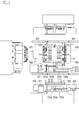
- the power conversion system 1 of this example directly converts the three-phase AC power supplied from the three-phase AC power source 2 into single-phase AC power by the power conversion device 3 according to the embodiment of the present invention, and converts this to the transformer 4
- the voltage is stepped up or down to an appropriate voltage and then converted into DC power by the rectifier 5 to charge the secondary battery 6.
- Reference numeral 7 denotes a smoothing circuit.
- each phase of the output lines (indicated by R phase, S phase, and T phase) supplied with three-phase AC power from the three-phase AC power source 2 attenuates harmonics as a noise countermeasure.
- a filter circuit 8 is provided.
- the filter circuit 8 of this example includes three filter reactors 81 connected to the phases R, S, and T, and six filter capacitors 82L and 82R connected between the phases R, S, and T.
- the layout of the filter capacitors 82L and 82R (shown as filter capacitors 821 to 836 in FIGS. 2 and 4) will be described later.
- the power conversion device 3 of this example includes six bidirectional switching elements 31 (311 to 316) arranged in a matrix corresponding to the R phase, S phase, and T phase.
- a single bidirectional switching element will be collectively described using reference numeral 31, while a specific element of the six bidirectional switching elements as shown in FIG. 1 will be described using 311 to 316. explain.
- Each of the bidirectional switching elements 31 of this example is composed of an IGBT module in which an IGBT, which is a semiconductor switching element, is combined with a free-wheeling diode and connected in reverse parallel. Note that the configuration of one bidirectional switching element 31 is not limited to that shown in the figure, but may be a configuration in which, for example, two reverse blocking IGBT elements are connected in antiparallel.
- Each of the bidirectional switching elements 31 includes an input side and an output of the bidirectional switching element 31 in order to protect the bidirectional switching element 31 from a surge voltage generated by the ON / OFF operation of the bidirectional switching element 31.
- a snubber circuit 32 (321 to 326) in which one snubber capacitor 327 (refer to the circuit diagram at the lower right in the figure) and three diodes are combined is provided on the side.
- reference numeral 32 is used to collectively refer to one snubber circuit
- reference numerals 321 to 326 are used to indicate a specific snubber circuit among the six snubber circuits as shown in FIG.
- the power conversion system 1 of the present example includes a matrix converter control circuit 9 for ON / OFF control of each of the bidirectional switching elements 31 of the power conversion device 3.
- the matrix converter control circuit 9 inputs the voltage value supplied from the three-phase AC power source 2, the DC current value currently being output, and the target current command value, and based on these, the respective gate signals of the bidirectional switching element 31 are supplied. By controlling and adjusting the single-phase AC power output to the transformer 4, DC power that matches the target is obtained.
- the transformer 4 boosts or lowers the voltage of the single-phase AC power converted by the power converter 3 to a predetermined value.
- the rectifier 5 includes four rectifier diodes 51 to 54, and converts the regulated single-phase AC power into DC power.
- the smoothing circuit 7 includes a coil 71 and a capacitor 72, and smoothes the pulsating flow included in the rectified direct current to a state closer to direct current.
- the three-phase AC power supplied from the three-phase AC power source 2 is directly converted into single-phase AC power by the power converter 3 and adjusted to an appropriate voltage. After being pressed, it is converted to DC power. Thereby, the secondary battery 6 is charged.
- the above-described power conversion system 1 is an example to which the power conversion device 3 according to the present invention is applied, and the present invention is not limited to application to the power conversion system 1. That is, as long as at least one of the conversion source power and the conversion destination power is polyphase AC power, it can be applied to other power conversion systems.
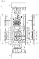
- FIG. 3 shows an assembly in which six bidirectional switching elements 31 (one of which is also referred to as an IGBT module) are mounted on the upper surface of the heat sink 10 and a bus bar for connecting the terminals of the bidirectional switching elements 31 is mounted thereon.
- FIG. 2 is a plan view showing a state in the middle.
- FIG. 2 is a plan view showing an assembled state in which three diodes constituting the snubber circuit 32 and six filter capacitors 82 of the filter circuit 8 are mounted thereon, right and left side views, and front view.
- the bidirectional switching element 31 of this example has an input terminal of the bidirectional switching element 31, an output terminal, and a midpoint terminal of two IGBTs that make a pair on the upper surface of the module package. Is provided.
- the leftmost terminals of the three bidirectional switching elements 311, 313 and 315 among the six bidirectional switching elements 311 to 316 shown in FIGS. 3 and 5 are hidden by the input terminals (in FIG. 3, they are hidden by the bus bars 333, 334 and 335.
- the rightmost terminal is the output terminal, and the middle terminal is the midpoint terminal.
- 3 and 5 are input terminals (in FIG. 3, bus bars 333, 334, and 335.
- the leftmost terminal is the output terminal, and the middle terminal is the midpoint terminal.
- the gate terminal of the bidirectional switching element 31 is provided in the other part of the module package.
- the six bidirectional switching elements 311 to 316 are fixed to the upper surface of the heat sink 10 by fixing means such as bolts.
- These six bidirectional switching elements 311 to 316 are composed of a pair of bidirectional switching elements 311 and 312, bidirectional switching elements 313 and 314, and bidirectional switching elements 315 and 316, respectively.
- two bidirectional switching elements 311 and 312 that are paired along the extending direction of three terminals (input terminal, intermediate point terminal, output terminal) of one bidirectional switching element 31, bidirectional switching element Reference numerals 313 and 314 and bidirectional switching elements 315 and 316 are arranged on the left and right of the center line CL, respectively.
- the paired bidirectional switching elements are a pair of bidirectional switching elements connected to the same phase R, S, T of the input line.
- the bidirectional switching elements 311 and 312, the bidirectional switching elements 313 and 314, and the bidirectional switching elements 315 and 316 that are paired are arranged side by side on the left and right sides of the center line CL, so that the output lines P and N (Bus bars 331a, 332a) can be drawn out in the shortest distance in one direction. If the wiring length to which the high-frequency AC power is output is long, it is easily affected by the L component. Therefore, according to the arrangement of this example, the influence of the L component can be suppressed. That is, output lines P and N including output lines that are at least near a straight line up to the transformer 4.
- the rightmost terminals of the bidirectional switching elements 311, 313, and 315 on the left side of the center line CL are all output terminals, and the leftmost terminals are all input terminals.
- the leftmost terminals of the bidirectional switching elements 312, 314, and 316 on the right side of the center line CL are all output terminals, and the rightmost terminals are all input terminals.
- the input lines R, S, and T of the three-phase AC power supply 2 are connected to the center line CL by the bus bars 333, 334, and 335 at the left end input terminals of the bidirectional switching elements 311, 313, and 315 on the left side of the center line CL.
- the input lines R configured such that these bus bars 333, 334, and 335 further extend to input terminals at the right ends of the bidirectional switching elements 312, 314, and 316 on the right side of the center line CL.
- S, T are connected.
- the R phase is connected to the input terminals of the bidirectional switching elements 311 and 312
- the S phase is connected to the input terminals of the bidirectional switching elements 313 and 314,
- the T phase is connected to the input terminals of the bidirectional switching elements 315 and 316.
- the bus bars 333, 334, and 335 as the input lines R, S, and T are drawn from one of the left and right sides and extended to the other side of the left and right, so that the distance in the left and right direction of the heat sink 10 can be shortened.
- the filter capacitors 82L and 82R to be arranged can be evenly arranged, which simplifies the layout and contributes to space saving.
- the bus bar 333 constituting the input line R connects between the input terminals of the paired bidirectional switching elements 311 and 312 arranged on the left and right of the center line CL, and the bus bar 334 constituting the input line S is both
- the bus bars 335 that connect the input terminals of the directional switching elements 313 and 314 and form the input line T connect the input terminals of the bidirectional switching elements 315 and 316.
- wirings corresponding to the bus bars 333, 334, and 335 are denoted by the same reference numerals. Note that the connection structure using the bus bars 333 to 335 is not essential for the function of the power conversion device 3.
- the filter capacitors 82L and 82R provided between the phases can be shared with each other. That is, a filter capacitor 821 is provided between the R phase and S phase on the left side of the figure, and a filter capacitor 824 is provided between the R phase and S phase on the right side, but the R phase is input.
- the input terminals of the bidirectional switching elements 311 and 312 are connected by a bus bar 333.
- the two filter capacitors 821 and 824 cooperate to filter the R-phase noise of the three-phase AC power supply 2, one filter capacitor can be reduced in size, resulting in a smaller filter capacitor. It will be possible. The same can be said for the S phase and the T phase.
- bus bars 333 to 335 intersect the bus bars 331 and 332 constituting the output lines P and N in a plan view, but as shown in the front views of FIGS.
- 332 By setting 332 at a position higher than the bus bars 333 to 335 connecting the input terminals, they are configured so that they do not interfere with each other by a three-dimensional intersection.
- the input lines R, S, T from the three-phase AC power source 2 to the power converter 3 are configured to branch between the filter reactor 81 and the filter capacitors 82L, 82R.
- the filter reactor 81 may be provided in each of the branched input lines R, S, and T.
- one bus bar 331a constituting the output line P of the power converter 3 is connected to the output terminal at the right end of the bidirectional switching elements 311, 313, 315 on the left side of the center line CL, while the center line
- One bus bar 332a constituting the output line N of the power converter 3 is connected to the left end output terminals of the bidirectional switching elements 312, 314, 316 on the right side of the CL.
- the front ends of these bus bars 331a and 332a are connected to the transformer 4.
- the following bus bars including these bus bars 331a and 332a are made of a conductive material such as copper.
- a pair of bus bars 331a and 332a constituting the output lines P and N of the power conversion device 3 are relatively wide with respect to bus bars 331b and 332b described later, as shown in the plan view and the front view of FIG.
- the heat sink 10 is arranged upright and side by side with respect to the main surface. Although the width dimension of these bus bars 331a and 332a is determined by the rated current, a large current can be caused to flow by the skin effect of the high-frequency current by forming it in a wide shape.
- the distance between the left bidirectional switching elements 311, 313 and 315 and the right bidirectional switching elements 312, 314 and 316 can be shortened, and power conversion The apparatus 3 can be reduced in the left-right direction.
- each of the bus bars 331b and 332b includes a plurality of ( In this example, two bus bars are arranged so as to be stacked at a predetermined interval.
- the connection terminals for the transformer 4 can be arranged in the same posture at the right end as shown in the plan view of FIG.
- the filter circuit 8 includes six filter capacitors 821 to 826, and three filter circuits 8 are arranged on each of the left and right input lines of the center line CL as shown in FIGS.
- the left filter capacitor 821 is provided between the R phase and the S phase corresponding to the input terminal of the bidirectional switching element 311.
- the left filter capacitor 822 is provided between the S phase and the T phase corresponding to the input terminal of the bidirectional switching element 313, and the left filter capacitor 823 corresponds to the input terminal of the bidirectional switching element 315.
- the T phase and the R phase Provided between the T phase and the R phase.
- the right filter capacitor 824 is provided between the R phase and the S phase corresponding to the input terminal of the bidirectional switching element 312, and the right filter capacitor 825 corresponds to the input terminal of the bidirectional switching element 314.
- the right filter capacitor 826 is provided between the S phase and the T phase, and the right filter capacitor 826 is provided between the T phase and the R phase corresponding to the input terminal of the bidirectional switching element 316.
- filter capacitors 821 to 826 correspond to the six bidirectional switching elements 311 to 316 arranged three on each side of the center line CL. By disposing them, it is possible to shorten the routing distance of the connection wirings of the filter capacitors 821 to 826 and the bidirectional switching elements 311 to 316.
- three filter capacitors 821 to 826 are arranged on the outer side with respect to the center line CL from the region where the six bidirectional switching elements 311 to 316 are provided. Specifically, as shown in FIGS. 2, 4, and 5, it is fixed to the upper part of bus bars 333, 334, and 335.
- the filter capacitors 821 to 826 By disposing the filter capacitors 821 to 826 outside the bidirectional switching elements 311 to 316, the distance between the left and right bidirectional switching elements 31L and 31R can be minimized, so that the distance of the heat sink 10 in the lateral direction is minimized.
- the distance can be set, and as a result, the heat sink 10 can be downsized as compared with the case where six filter capacitors are arranged in the center.
- the bus bar 331a connects the output terminals of the bidirectional switching elements 311, 313, and 315, and the output line reaches the transformer 4 through the bus bar 331b.
- the bus bar 332a is an output line N that connects the output terminals of the bidirectional switching elements 312, 314, and 316 and reaches the transformer 4 via the bus bar 332b.
- the bus bar 333 is a bus bar to which the input line R phase is connected and which connects the input terminals of the bidirectional switching elements 311 and 312.
- the bus bar 333 extends to the outside of the left and right sides of both input terminals and includes filter capacitors 821, 823 and 824. , 826 are directly connected.
- the bus bar 334 is a bus bar to which the input line S phase is connected and which connects the input terminals of the bidirectional switching elements 313 and 314.
- the bus bar 334 extends outward from the left and right sides of the input terminals. 822, 824, and 825 are directly connected.
- the bus bar 335 is a bus bar to which the input line T-phase is connected and which connects the input terminals of the bidirectional switching elements 315 and 316.
- the bus bar 335 extends to the left and right outside both the input terminals, and is connected to the filter capacitors 822, 823, and 825 here. , 826 are directly connected. Since the filter capacitors 821 to 826 are directly connected to the bus bars 333 to 335 in this way, the connection structure is simplified.
- three filter capacitors 82L and 82R arranged on each of the left and right sides are arranged on the outer side with respect to the center line CL, and one vertex is directed to the outward direction (
- the filter capacitors 821, 822, and 823 are arranged so that the centers thereof are positioned at the respective vertices of an isosceles triangle or an equilateral triangle.
- the filter capacitors 821 to 826 are arranged on the upper surface of the bus bar, in other words, on the opposite side of the bus bar from the bidirectional switching elements 311 to 316, so that the layout of the filter capacitors 821 to 826 is achieved.
- the degree of design freedom increases.
- the snubber circuit 321 of the bidirectional switching element 311 has one terminal connected to the input terminal of the bidirectional switching element 311 and the other terminal connected to the midpoint terminal of the bidirectional switching element 311. Are connected to the output terminal of the bidirectional switching element 311. Therefore, as shown in FIG. 2, the three diodes are respectively fixed and connected to brackets 351 to 356 made of conductors connected to the intermediate point terminals of the bidirectional switching elements 31L and 31R.
- a relatively large electrolytic capacitor is used as the snubber capacitor 327, and the snubber capacitor 327 common to the six snubber circuits 321 to 326 is used (see FIG. 2).
- the snubber capacitor 327 and the three diodes are connected by wiring.
- filter capacitors 821 to 826 are arranged three to the left and right of the center line CL with respect to the six bidirectional switching elements 311 to 316 arranged three to the left and right of the center line CL, respectively. Since they are arranged correspondingly, it is possible to shorten the distance between the connection wirings of the filter capacitors 821 to 826 and the bidirectional switching elements 311 to 316.
- the bidirectional switching elements 311 and 312, the bidirectional switching elements 313 and 314, and the bidirectional switching elements 315 and 316 are arranged side by side on the left and right sides of the center line CL.
- the layout is such that the lines P and N (bus bars 331a and 332a) can be drawn short in one direction. Therefore, if the wiring length from which the high-frequency AC power is output is long, it is easily affected by the L component, but according to the arrangement of this example, the influence of the L component can be suppressed.
- the pair of bus bars 331a and 332a configuring the output lines P and N are relatively wide with respect to the bus bars 331b and 332b, and are arranged upright with respect to the main surface of the heat sink 10.
- a large current can flow due to the skin effect of the high-frequency current.
- the distance between the left bidirectional switching elements 311, 313 and 315 and the right bidirectional switching elements 312, 314 and 316 can be shortened, and power conversion The apparatus 3 can be reduced in the left-right direction.
- the pair of bus bars 331b and 332b constituting the output lines P and N are formed relatively narrow with respect to the bus bars 331a and 332a, but a plurality of bus bars are predetermined for one bus bar. They are stacked at intervals, and are arranged in a horizontal direction with respect to the main surface of the heat sink 10. Since the bus bars 331b and 332b are formed to be relatively narrow with respect to the bus bars 331a and 332a, the exclusive use of the space is minimal, and the bus bars 331b and 332b can be arranged side by side in the horizontal direction. It can be arranged in a posture. In addition, since a plurality of bus bars are stacked at a predetermined interval in one bus bar, a high-frequency current equivalent to that of the bus bars 331a and 332a can flow due to the skin effect.
- the three filter capacitors 821 to 826 on each of the left and right are disposed outside the center line CL from the region where the six bidirectional switching elements 311 to 316 are provided.
- the distance between the left and right bidirectional switching elements 31L and 31R can be minimized. Therefore, the distance in the left-right direction of the heat sink 10 can be set to the shortest distance, and as a result, the heat sink 10 can be reduced in size.
- the bus bars 333, 334, and 335 constituting the input line are drawn from one of the left and right sides, and extend to the other side of the left and right, thereby forming a pair of bidirectional switching elements arranged on the left and right of the center line CL Input terminals of 311 and 312, bidirectional switching elements 313 and 314, and bidirectional switching elements 325 and 316 are connected to each other.
- the distance in the left-right direction of the heat sink 10 can be shortened, and filter capacitors 82L and 82R, which will be described later, can be evenly arranged, thereby simplifying the layout and contributing to space saving.
- the filter capacitors 82L and 82R provided between the phases can be shared with each other, one filter capacitor can be reduced in capacity, and as a result, the filter capacitor can be reduced in size.
- the filter capacitors 821 to 826 are disposed on the upper surfaces of the bus bars 333, 334, and 335, in other words, on the opposite side of the bus bars from the bidirectional switching elements 311 to 316. Therefore, the degree of freedom in designing the layout of the filter capacitors 821 to 826 is increased.
- the wiring length between the capacitors can be set to the shortest distance, and the power conversion device 3 can be downsized. It is also possible to tune between capacitors.
- the three filter capacitors 82L and 82R on the left and right are arranged outside the bidirectional switching elements 311, 313, 315 and 312, 314, 316 with respect to the center line CL. It can also be arranged between the bidirectional switching elements 311, 313, 315 and 312, 314, 316 arranged on the left and right with respect to CL.
- the six bidirectional switching elements 311 to 316 are disposed on the left side with respect to the center line CL, and the bidirectional switching elements 312, 314, 314 are disposed on the right side.
- the bidirectional switching elements 311, 313 and 315 and the bidirectional switching elements 312, 314 and 316 may be disposed along the center line CL.
- the six bidirectional switching elements 311 to 316 are disposed on the left side with respect to the center line CL, and the bidirectional switching elements 312, 314, 314 are disposed on the right side.
- the input and output terminals of each bidirectional switching element are arranged symmetrically with respect to the center line CL, but the bidirectional switching elements 311, 313 and 315 are arranged on the left side with respect to the center line CL.
- the bidirectional switching elements 312, 314, and 316 may be arranged on the right side, and the input terminals and output terminals of the bidirectional switching elements may be arranged in the same manner.
- the filter capacitors 821 to 826 are provided between the phases so as to correspond to each of the six bidirectional switching elements 311 to 316, but the six bidirectional switching elements 311 to 316 are provided.
- Filter capacitors 821 to 826 may be provided between the phases so as to correspond to each of 316.
- the filter capacitor may be arranged at the center of the power conversion device 3 or outside the power conversion device 3. If it arrange
- the bidirectional switching elements 311, 313, 315 correspond to the first switching means according to the present invention
- the bidirectional switching elements 312, 314, 316 correspond to the second switching means according to the present invention
- the power conversion device 3 corresponds to the conversion circuit according to the present invention
- the bus bars 331a and 332a correspond to the first output line according to the present invention
- the bus bars 331b and 332b correspond to the second output line according to the present invention.
Landscapes
- Engineering & Computer Science (AREA)
- Power Engineering (AREA)
- Microelectronics & Electronic Packaging (AREA)
- Ac-Ac Conversion (AREA)
- Inverter Devices (AREA)
Abstract
Priority Applications (4)
| Application Number | Priority Date | Filing Date | Title |
|---|---|---|---|
| CN201280049145.XA CN103858329B (zh) | 2011-10-07 | 2012-09-28 | 电力变换装置 |
| US14/349,686 US9369055B2 (en) | 2011-10-07 | 2012-09-28 | Power converter |
| EP12838013.6A EP2765700B1 (fr) | 2011-10-07 | 2012-09-28 | Convertisseur de puissance |
| JP2013537349A JP5420122B2 (ja) | 2011-10-07 | 2012-09-28 | 電力変換装置 |
Applications Claiming Priority (2)
| Application Number | Priority Date | Filing Date | Title |
|---|---|---|---|
| JP2011-223289 | 2011-10-07 | ||
| JP2011223289 | 2011-10-07 |
Publications (1)
| Publication Number | Publication Date |
|---|---|
| WO2013051476A1 true WO2013051476A1 (fr) | 2013-04-11 |
Family
ID=48043636
Family Applications (1)
| Application Number | Title | Priority Date | Filing Date |
|---|---|---|---|
| PCT/JP2012/075097 WO2013051476A1 (fr) | 2011-10-07 | 2012-09-28 | Convertisseur de puissance |
Country Status (5)
| Country | Link |
|---|---|
| US (1) | US9369055B2 (fr) |
| EP (1) | EP2765700B1 (fr) |
| JP (1) | JP5420122B2 (fr) |
| CN (1) | CN103858329B (fr) |
| WO (1) | WO2013051476A1 (fr) |
Cited By (1)
| Publication number | Priority date | Publication date | Assignee | Title |
|---|---|---|---|---|
| JP2019004582A (ja) * | 2017-06-14 | 2019-01-10 | 三菱電機株式会社 | 開閉モジュール用のコンデンサ基板ユニット、開閉モジュール、およびモータ駆動装置 |
Families Citing this family (7)
| Publication number | Priority date | Publication date | Assignee | Title |
|---|---|---|---|---|
| JP5377575B2 (ja) * | 2011-05-31 | 2013-12-25 | 日産自動車株式会社 | 電力変換装置 |
| JP5377574B2 (ja) | 2011-05-31 | 2013-12-25 | 日産自動車株式会社 | 電力変換装置 |
| JP5437312B2 (ja) | 2011-05-31 | 2014-03-12 | 日産自動車株式会社 | 電力変換装置 |
| EP2765699B1 (fr) * | 2011-10-07 | 2017-03-29 | Nissan Motor Co., Ltd | Convertisseur de puissance |
| EP3180849B1 (fr) * | 2014-08-13 | 2021-11-10 | INESC TEC - Instituto de Engenharia de Sistemas e Computadores, Tecnologia e Ciência | Convertisseur ca/cc avec convertisseur matriciel trois à une phase, convertisseur ca/cc de pont complet et transformateur de haute frequence |
| US11251618B2 (en) * | 2015-01-21 | 2022-02-15 | Enphase Energy, Inc. | Apparatus and method for reactive power control |
| WO2017038294A1 (fr) * | 2015-08-28 | 2017-03-09 | 株式会社村田製作所 | Convertisseur continu/continu |
Citations (6)
| Publication number | Priority date | Publication date | Assignee | Title |
|---|---|---|---|---|
| JPH02130955A (ja) * | 1988-11-11 | 1990-05-18 | Fuji Electric Co Ltd | 逆阻止形トランジスタモジュール |
| JP2001045772A (ja) * | 1999-08-03 | 2001-02-16 | Yaskawa Electric Corp | 3レベルインバータまたはpwmサイクロコンバータ |
| JP2004236374A (ja) * | 2003-01-28 | 2004-08-19 | Fuji Electric Holdings Co Ltd | 交流−交流直接変換形電力変換装置の構成方法 |
| JP2005065357A (ja) * | 2003-08-12 | 2005-03-10 | Hitachi Ltd | マトリクスコンバータシステム |
| JP2006333590A (ja) | 2005-05-25 | 2006-12-07 | Fuji Electric Fa Components & Systems Co Ltd | Ac−ac電力変換装置 |
| JP2011120358A (ja) * | 2009-12-02 | 2011-06-16 | Denso Corp | 電力変換装置 |
Family Cites Families (15)
| Publication number | Priority date | Publication date | Assignee | Title |
|---|---|---|---|---|
| JPH06261556A (ja) * | 1993-03-04 | 1994-09-16 | Toshiba Corp | 半導体スイッチ装置 |
| JP4385672B2 (ja) * | 2003-08-12 | 2009-12-16 | 株式会社日立製作所 | マトリクスコンバータを使用した電力変換装置 |
| DE112007000366T5 (de) * | 2006-02-17 | 2009-01-02 | Kabushiki Kaisha Yaskawa Denki, Kitakyushu | Leistungsumwandlungsvorrichtung mit Sammelschiene |
| JP4720756B2 (ja) * | 2007-02-22 | 2011-07-13 | トヨタ自動車株式会社 | 半導体電力変換装置およびその製造方法 |
| US20090052134A1 (en) * | 2007-08-22 | 2009-02-26 | Casteel Jordan B | Liquid-cooled grounded heatsink for diode rectifier system |
| EP2099119B1 (fr) * | 2008-03-04 | 2014-11-19 | Kabushiki Kaisha Toyota Jidoshokki | Appareil convertisseur de puissance |
| JP2012054449A (ja) * | 2010-09-02 | 2012-03-15 | Aisin Aw Co Ltd | 電気的接続装置 |
| EP2512023A3 (fr) * | 2011-04-14 | 2017-06-28 | General Electric Technology GmbH | Agencement de convertisseur de puissance et procédé pour exploiter un agencement de convertisseur de puissance |
| JP5377575B2 (ja) * | 2011-05-31 | 2013-12-25 | 日産自動車株式会社 | 電力変換装置 |
| JP5377574B2 (ja) * | 2011-05-31 | 2013-12-25 | 日産自動車株式会社 | 電力変換装置 |
| JP5437312B2 (ja) * | 2011-05-31 | 2014-03-12 | 日産自動車株式会社 | 電力変換装置 |
| JP5437313B2 (ja) * | 2011-05-31 | 2014-03-12 | 日産自動車株式会社 | 電力変換装置 |
| JP5377573B2 (ja) * | 2011-05-31 | 2013-12-25 | 日産自動車株式会社 | 電力変換装置 |
| JP5437314B2 (ja) * | 2011-05-31 | 2014-03-12 | 日産自動車株式会社 | 電力変換装置 |
| EP2765699B1 (fr) * | 2011-10-07 | 2017-03-29 | Nissan Motor Co., Ltd | Convertisseur de puissance |
-
2012
- 2012-09-28 US US14/349,686 patent/US9369055B2/en active Active
- 2012-09-28 CN CN201280049145.XA patent/CN103858329B/zh not_active Expired - Fee Related
- 2012-09-28 EP EP12838013.6A patent/EP2765700B1/fr not_active Not-in-force
- 2012-09-28 JP JP2013537349A patent/JP5420122B2/ja not_active Expired - Fee Related
- 2012-09-28 WO PCT/JP2012/075097 patent/WO2013051476A1/fr active Application Filing
Patent Citations (6)
| Publication number | Priority date | Publication date | Assignee | Title |
|---|---|---|---|---|
| JPH02130955A (ja) * | 1988-11-11 | 1990-05-18 | Fuji Electric Co Ltd | 逆阻止形トランジスタモジュール |
| JP2001045772A (ja) * | 1999-08-03 | 2001-02-16 | Yaskawa Electric Corp | 3レベルインバータまたはpwmサイクロコンバータ |
| JP2004236374A (ja) * | 2003-01-28 | 2004-08-19 | Fuji Electric Holdings Co Ltd | 交流−交流直接変換形電力変換装置の構成方法 |
| JP2005065357A (ja) * | 2003-08-12 | 2005-03-10 | Hitachi Ltd | マトリクスコンバータシステム |
| JP2006333590A (ja) | 2005-05-25 | 2006-12-07 | Fuji Electric Fa Components & Systems Co Ltd | Ac−ac電力変換装置 |
| JP2011120358A (ja) * | 2009-12-02 | 2011-06-16 | Denso Corp | 電力変換装置 |
Non-Patent Citations (1)
| Title |
|---|
| See also references of EP2765700A4 |
Cited By (2)
| Publication number | Priority date | Publication date | Assignee | Title |
|---|---|---|---|---|
| JP2019004582A (ja) * | 2017-06-14 | 2019-01-10 | 三菱電機株式会社 | 開閉モジュール用のコンデンサ基板ユニット、開閉モジュール、およびモータ駆動装置 |
| US10305389B2 (en) | 2017-06-14 | 2019-05-28 | Mitsubishi Electric Corporation | Capacitor substrate unit for opening/closing module |
Also Published As
| Publication number | Publication date |
|---|---|
| CN103858329A (zh) | 2014-06-11 |
| EP2765700B1 (fr) | 2017-04-26 |
| US9369055B2 (en) | 2016-06-14 |
| US20140247635A1 (en) | 2014-09-04 |
| JP5420122B2 (ja) | 2014-02-19 |
| EP2765700A1 (fr) | 2014-08-13 |
| CN103858329B (zh) | 2017-03-29 |
| JPWO2013051476A1 (ja) | 2015-03-30 |
| EP2765700A4 (fr) | 2016-04-13 |
Similar Documents
| Publication | Publication Date | Title |
|---|---|---|
| JP5476510B2 (ja) | 電力変換装置 | |
| JP5420122B2 (ja) | 電力変換装置 | |
| JP5377575B2 (ja) | 電力変換装置 | |
| JP5437314B2 (ja) | 電力変換装置 | |
| JP5437312B2 (ja) | 電力変換装置 | |
| JP5437313B2 (ja) | 電力変換装置 | |
| JP5377573B2 (ja) | 電力変換装置 | |
| JP5377574B2 (ja) | 電力変換装置 |
Legal Events
| Date | Code | Title | Description |
|---|---|---|---|
| 121 | Ep: the epo has been informed by wipo that ep was designated in this application |
Ref document number: 12838013 Country of ref document: EP Kind code of ref document: A1 |
|
| ENP | Entry into the national phase |
Ref document number: 2013537349 Country of ref document: JP Kind code of ref document: A |
|
| WWE | Wipo information: entry into national phase |
Ref document number: 14349686 Country of ref document: US |
|
| NENP | Non-entry into the national phase |
Ref country code: DE |
|
| REEP | Request for entry into the european phase |
Ref document number: 2012838013 Country of ref document: EP |
|
| WWE | Wipo information: entry into national phase |
Ref document number: 2012838013 Country of ref document: EP |