EP2709154A2 - Halbleiterbauelement und Verfahren zu seiner Herstellung - Google Patents
Halbleiterbauelement und Verfahren zu seiner Herstellung Download PDFInfo
- Publication number
- EP2709154A2 EP2709154A2 EP13184152.0A EP13184152A EP2709154A2 EP 2709154 A2 EP2709154 A2 EP 2709154A2 EP 13184152 A EP13184152 A EP 13184152A EP 2709154 A2 EP2709154 A2 EP 2709154A2
- Authority
- EP
- European Patent Office
- Prior art keywords
- wide band
- doped
- gap semiconductor
- thyristor
- unit
- Prior art date
- Legal status (The legal status is an assumption and is not a legal conclusion. Google has not performed a legal analysis and makes no representation as to the accuracy of the status listed.)
- Granted
Links
Images



Classifications
-
- H—ELECTRICITY
- H10—SEMICONDUCTOR DEVICES; ELECTRIC SOLID-STATE DEVICES NOT OTHERWISE PROVIDED FOR
- H10D—INORGANIC ELECTRIC SEMICONDUCTOR DEVICES
- H10D84/00—Integrated devices formed in or on semiconductor substrates that comprise only semiconducting layers, e.g. on Si wafers or on GaAs-on-Si wafers
- H10D84/201—Integrated devices formed in or on semiconductor substrates that comprise only semiconducting layers, e.g. on Si wafers or on GaAs-on-Si wafers characterised by the integration of only components covered by H10D1/00 or H10D8/00, e.g. RLC circuits
- H10D84/204—Integrated devices formed in or on semiconductor substrates that comprise only semiconducting layers, e.g. on Si wafers or on GaAs-on-Si wafers characterised by the integration of only components covered by H10D1/00 or H10D8/00, e.g. RLC circuits of combinations of diodes or capacitors or resistors
-
- H—ELECTRICITY
- H10—SEMICONDUCTOR DEVICES; ELECTRIC SOLID-STATE DEVICES NOT OTHERWISE PROVIDED FOR
- H10D—INORGANIC ELECTRIC SEMICONDUCTOR DEVICES
- H10D18/00—Thyristors
- H10D18/01—Manufacture or treatment
-
- H—ELECTRICITY
- H10—SEMICONDUCTOR DEVICES; ELECTRIC SOLID-STATE DEVICES NOT OTHERWISE PROVIDED FOR
- H10D—INORGANIC ELECTRIC SEMICONDUCTOR DEVICES
- H10D84/00—Integrated devices formed in or on semiconductor substrates that comprise only semiconducting layers, e.g. on Si wafers or on GaAs-on-Si wafers
- H10D84/101—Integrated devices comprising main components and built-in components, e.g. IGBT having built-in freewheel diode
- H10D84/131—Thyristors having built-in components
- H10D84/135—Thyristors having built-in components the built-in components being diodes
-
- H—ELECTRICITY
- H10—SEMICONDUCTOR DEVICES; ELECTRIC SOLID-STATE DEVICES NOT OTHERWISE PROVIDED FOR
- H10D—INORGANIC ELECTRIC SEMICONDUCTOR DEVICES
- H10D84/00—Integrated devices formed in or on semiconductor substrates that comprise only semiconducting layers, e.g. on Si wafers or on GaAs-on-Si wafers
- H10D84/60—Integrated devices formed in or on semiconductor substrates that comprise only semiconducting layers, e.g. on Si wafers or on GaAs-on-Si wafers characterised by the integration of at least one component covered by groups H10D10/00 or H10D18/00, e.g. integration of BJTs
- H10D84/676—Combinations of only thyristors
-
- H—ELECTRICITY
- H10—SEMICONDUCTOR DEVICES; ELECTRIC SOLID-STATE DEVICES NOT OTHERWISE PROVIDED FOR
- H10F—INORGANIC SEMICONDUCTOR DEVICES SENSITIVE TO INFRARED RADIATION, LIGHT, ELECTROMAGNETIC RADIATION OF SHORTER WAVELENGTH OR CORPUSCULAR RADIATION
- H10F39/00—Integrated devices, or assemblies of multiple devices, comprising at least one element covered by group H10F30/00, e.g. radiation detectors comprising photodiode arrays
- H10F39/10—Integrated devices
- H10F39/103—Integrated devices the at least one element covered by H10F30/00 having potential barriers, e.g. integrated devices comprising photodiodes or phototransistors
-
- H—ELECTRICITY
- H10—SEMICONDUCTOR DEVICES; ELECTRIC SOLID-STATE DEVICES NOT OTHERWISE PROVIDED FOR
- H10F—INORGANIC SEMICONDUCTOR DEVICES SENSITIVE TO INFRARED RADIATION, LIGHT, ELECTROMAGNETIC RADIATION OF SHORTER WAVELENGTH OR CORPUSCULAR RADIATION
- H10F39/00—Integrated devices, or assemblies of multiple devices, comprising at least one element covered by group H10F30/00, e.g. radiation detectors comprising photodiode arrays
- H10F39/80—Constructional details of image sensors
- H10F39/803—Pixels having integrated switching, control, storage or amplification elements
Definitions
- This invention relates generally to semiconductor devices and methods for making the same. More particularly, this invention relates to optically triggered semiconductor devices employing thyristor devices and methods for making the same.
- Thyristor devices such as silicon controlled rectifiers (SCRs) have been widely used as switching devices in a variety of applications, such as motor controls, home appliances, power converters, and light dimmers due to their fast response time, regenerative action and low resistance thereof once triggered.
- SCRs silicon controlled rectifiers
- the thyristor devices are used as power semiconductor switches that permit large electrical currents to be switched at high voltages.
- the thyristor devices are triggered to be electrically conductive by applying a trigger current to their gate terminals, while the anode and cathode terminals thereof are forward biased.
- the gate trigger current may be removed without turning off the thyristor devices.
- the thyristor devices become low-impedance current paths and remain in the conductive state until an electric current flowing between the anode and cathode terminals is reduced below a minimum value called the holding current.
- the anode and cathode terminals may be reverse biased to turn off the thyristor devices.
- thyristor devices There have been various ways to trigger the thyristor devices through the gate terminals thereof.
- an incident light is applied to a thyristor device to generate a trigger current through by means of the photoelectric effect to trigger the thyristor device.
- Using incident light to trigger thyristor devices for high voltage applications is advantageous because the incident light can be isolated from the anode and cathode terminals of the thyristor devices.
- a semiconductor device in accordance with one aspect of the invention.
- the semiconductor device includes an avalanche photodiode unit and a thyristor unit.
- the avalanche photodiode unit is configured to receive incident light to generate a trigger current and comprises a wide band-gap semiconductor.
- the thyristor unit is configured to be activated by the trigger current to an electrically conductive state.
- the semiconductor device includes a wide band-gap semiconductor body.
- the wide band-gap semiconductor body includes an avalanche photodiode unit and a thyristor unit.
- the avalanche photodiode unit is configured to receive incident light to generate a trigger current.
- the thyristor unit is configured to receive and be activated by the trigger current to an electrically conductive state.
- the avalanche photodiode unit and the thyristor unit are integrally formed on the wide band-gap semiconductor body.
- the semiconductor unit further includes an anode and a cathode conductively coupled to the wide band-gap semiconductor body, so that an electrical connection is provided between the anode and the cathode when the thyristor unit is in the electrically conductive state.
- a method for making a semiconductor device is also provided, in accordance with yet another aspect of the invention.
- the method includes providing a wide band-gap semiconductor body comprising four doped wide band-gap semiconductor layers each oppositely doped from an adjacent one of the doped wide band-gap semiconductor layers, defining an avalanche photodiode unit and a thyristor unit on the wide band-gap semiconductor body, and conductively coupling an anode and a cathode to respective ones of first and fourth doped wide band-gap semiconductor layers.
- the suffix "(s)" is usually intended to include both the singular and the plural of the term that it modifies, thereby including one or more of that term (e.g., "the element” may include one or more elements, unless otherwise specified).
- a particular configuration means that a particular element (e.g., feature, structure, and/or characteristic) described in connection with the configuration is included in at least one configuration described herein, and may or may not be present in other configurations.
- the described inventive features may be combined in any suitable manner in the various embodiments and configurations.
- approximating language may be applied to modify any quantitative representation that could permissibly vary without resulting in a change in the basic function to which it is related. Accordingly, a value modified by a term or terms, such as "about”, is not limited to the precise value specified. In some instances, the approximating language may correspond to the precision of an instrument for measuring the value.
- disposed on and “adjacent” refer to layers disposed directly in contact with each other or indirectly by having intervening layers there between.
- FIG. 1 is a schematic diagram of a switching system 10 employing a semiconductor device 11, in accordance with aspects of the present invention.
- the switching system 10 comprises a semiconductor device 11 onfigured to switch electrical power from an electrical power source 13 to a load 14, such as a power grid or other suitable devices.
- the electrical power source 13 may apply a high voltage to the semiconductor device 11.
- a single semiconductor device 11 is illustrated, more than one semiconductor device 11 may also be employed depending on the particular application.
- the semiconductor device 11 is an optically triggered semiconductor device.
- Incident light 12 from a light source may be applied to the semiconductor device 11 to generate a trigger current by means of the photoelectric effect to trigger or activate the semiconductor device 11.
- Non-limiting examples of the light source include light emitting diodes, ultraviolet light sources, or other suitable light sources.
- the semiconductor device 11 Before it is triggered, the semiconductor device 11 is in a non-conductive state. In this state, an electric current from the power source 13 cannot flow through the semiconductor device 11 to the load 14. Once triggered, the semiconductor device 11 is switched to an electrically conductive state, and the electric current from the power source 13 flows through the semiconductor device 11 to provide an electrical connection between the power source 13 and the load 14.
- the trigger current may be removed without turning off the electrical connection between the power source 13 and the load 14.
- the semiconductor device 11 When the electric current from the power source 13 is usually reduced below a minimum value called the holding current, the semiconductor device 11 returns to the non-conductive state to close the electrical connection between the power source 13 and the load 14.
- the switching system 10 may comprise other elements (not shown), such as a control unit for controlling the light source and/or the power source, passive components (e.g. inductors, capacitors), and other semiconductor devices.
- FIG. 2 is a schematic cross sectional diagram of the semiconductor device 11, in accordance with aspects of the present invention.
- the semiconductor device 11 comprises a semiconductor body 16.
- the semiconductor body 16 comprises a wide band-gap semiconductor and includes a number of doped wide band-gap semiconductor layers, such as first, second, third, and fourth doped layers 17-20.
- the second and the third doped wide band-gap semiconductor layers 18, 19 are disposed between the first and the fourth doped wide band-gap semiconductor layers 17, 20.
- the second doped wide band-gap semiconductor layer 18 is disposed between the first and the third doped wide band-gap semiconductor layers 17, 19, and the third doped wide band-gap semiconductor layer 19 is disposed between the second and the fourth doped wide band-gap semiconductor layers 18, 20.
- the wide band-gap semiconductor body 16 comprises silicon carbide.
- the wide band-gap semiconductor body 16 may comprise any other suitable wide bandgap material, such as gallium nitride (GaN), gallium phosphide (GaP), or aluminum gallium arsenide (AlGaAs).
- GaN gallium nitride
- GaP gallium phosphide
- AlGaAs aluminum gallium arsenide
- the first and the third doped layers 17, 19 may be p-doped layers, such as layers doped with a p-type dopant
- the second and the fourth doped layers 18, 20 may be n-type doped layers, such as layers doped with an n-type dopant, such that the wide band-gap semiconductor body 16 has a n-p-n-p structure along a direction from the fourth doped layer 20 to the first doped layer 17.
- n-type and p-type refer to the majority of charge carriers, which are present in a respective layer.
- the majority carriers are electrons
- the majority carriers are holes (the absence of electrons).
- the p-type dopant may comprise boron and/or aluminum.
- the n-type dopant may comprise nitrogen.
- the first and the fourth doped layers 17, 20 may be more heavily doped than the second and the third layers 18, 19.
- the first and the third layers 17, 19 may be n-doped layers
- the second and the fourth layers 18, 20 may be p-doped layers, such that the wide band-gap semiconductor body 16 has a p-n-p-n structure along the direction from the fourth doped layer 20 to the first doped layer 17.
- the first doped layer 17 of the wide band-gap semiconductor body 16 is discontinuous, and a separation slot 21 extends along and divides the first doped layer 17 into first and second portions 23, 24.
- the separation slot 21 extends downward into the second doped layer 18 along the first doped layer 17.
- the separation slot 21 may not extend into the second doped layer 18.
- the wide band-gap semiconductor body 16 is spatially formed with a first unit 25 and a second unit 26 unitary with the first unit 25 according to the position of the separation slot 21.
- the first doped layer 17 of the second section 26 also defines a light adsorption region 27 to absorb the incident light 12 from a light source (not labeled).
- the first unit 25 may act as a thyristor unit
- the second unit 26 may act as an avalanche photodiode unit.
- the avalanche photodiode unit 26 and the thyristor 25 are integrally formed on the wide band-gap semiconductor body.
- the semiconductor device 11 further comprises a first and a second electrically conductive layer 28, 29, which are typically formed of metal, such as aluminum-titanium-nickel multilayer (for the anode) and nickel (cathode).
- the first conductive layer 28 is disposed adjacent to a bottom surface 15 of the fourth layer 20.
- adjacent it is meant that the first conductive layer 28 may be disposed directly adjacent to the bottom surface 15 of the fourth layer 20 or there may be intervening layers. What is important is that the first conductive layer 28 be in ohmic contact with the fourth layer 20.
- the second conductive layer 29 is disposed adjacent (either directly adjacent or via intervening layer(s)) to upper surfaces (not labeled) of the first and the second portions 23, 24 of the first doped layer 17 respectively, such that the second conductive layer 29 is in ohmic contact with the first and the second portions 23, 24 of the first doped layer 17.
- the second conductive layer 29 may be disposed on different portions of the first doped layer 17.
- the first and the second conductive layers 28, 29 are configured to act as electrode terminals to electrically connect to the power source 13 and the load 14 (shown in FIG. 1 ).
- the first and the second conductive layers 28, 29 act as a cathode and an anode, respectively.
- a dielectric layer 30 is disposed on the first portion 23 of the first doped layer 17 to protect the first portion 23.
- the dielectric layer 30 may also be disposed within the separation slot 21 to protect the exposed second doped layer 18 and to electrically insulate the first and the second portions 23, 24 of the first doped layer 17.
- the first conductive layer 28 may also be covered by the dielectric layer 30.
- the dielectric layer 30 comprises silicon dioxide.
- the dielectric layer 30 may optionally comprise silicon nitride.
- An antireflection layer (not labeled) may be optionally disposed on the light absorption region 27 to facilitate absorption of the incident light 12 and protect the second portion 24 of the first doped layer 17.
- a wide band-gap semiconductor body 16 formed with multiple doped wide band-gap semiconductor layers 17-20 is provided.
- the thyristor unit 25 and the avalanche photodiode unit 26 are defined on the wide band-gap semiconductor body 16.
- the separation slot 21 is defined along the first doped layer 17 to define the avalanche photodiode unit 26 and the thyristor unit 25.
- the anode(s) 29 and cathode 28 are provided to be conductively coupled to the upper surface(s) of the first layer 17 and the bottom surface of the fourth doped layer 20.
- the sequence of defining the thyristor unit 25 and the avalanche photodiode unit 26, and providing the anode 29 and the cathode 28 may vary.
- the dielectric layer 30 may be also provided.
- the thyristor unit 25 is configured to switch the electrical connection between the power source 13 and the load 14.
- the anode 29 is electrically connected with the power source 13.
- the cathode 28 is electrically connected with the load 104.
- the anode 29 may be electrically connected with the load 104 while the cathode 28 may be electrically connected with the power source 13.
- the thyristor unit 25 may be turned on or activated by the trigger current to allow the electric current from the power source 13 to flow to the load 14 while the cathode 28 and the anode 29 thereof are forward biased. In other applications, the thyristor unit 25 may also be switched to the non-conductive state when the electric current from the power source 13 is reduced below the minimum value. Alternatively, the cathode 28 and the anode 29 may be reverse biased to turn off the thyristor unit 25.
- each of the four doped wide band-gap semiconductor layers 17-20 is oppositely doped from the adjacent layer(s), and a number of semiconductor junctions J1, J2, and J3 are formed at interfaces (not labeled) between the first and the second doped layers 17-18, between the second and the third doped layers 18-19, and between the third and the fourth doped layers 19-20 respectively in the thyristor unit 25.
- the trigger current may be injected into the second and/or the third doped layers (or a gate terminal) 18-19 to activate the thyristor unit 25.
- the avalanche photodiode unit 26 is configured to generate the trigger current by means of the photoelectric effect to activate the thyristor unit 25 when the incident light 12 is applied to the light absorption region 27 thereof while the avalanche photodiode unit 26 is reverse biased. Similar to the thyristor unit 25, a number of semiconductor junctions J1', J2', and J3' are also formed at the interfaces between the first and the second doped layers 17-18, between the second and the third doped layers 18-19, and between the third and the fourth doped layers 19-20 respectively in the avalanche photodiode unit 26. In the illustrated example, the semiconductor junctions J1', J2', and J3' are the same as the respective semiconductor junctions J1, J2, and J3.
- the injection of carriers may produce a large number of new carriers, resulting in an increase of the electric current.
- the amplification is accomplished during the avalanche breakdown, so that a large electric current may be obtained with an injection of a small number of carriers.
- the avalanche photodiode unit 26 uses photoinduced carriers produced by the optical absorption for the carrier injection that triggers this phenomenon.
- the incident light 12 is applied to the light absorption region 27 of the first doped layer 17 to induce the carriers (or a photoinduced electric current) while the semiconductor junction J1' is reverse biased.
- the incident light 12 may be ultraviolet (UV) light having a wavelength of between about 200 and about 450 nanometers.
- the incident light 12 has a wavelength of about 285 nanometers, and the semiconductor body 16 comprises silicon carbide with a photodiode sensitivity of about 0.14 amps per watt (A/W).
- Different wavelengths and/or energies of the incident light 12 may include different amounts of the carriers in the wide band-gap semiconductor body 16.
- the photoinduced carriers may be accelerated by the electrical field applied to the avalanche photodiode unit 26 to flow to the second and/or the third doped layers 18-19 to produce a large number of new carriers, resulting in a large electric current.
- Such a large electric current from the avalanche photodiode unit 26 acts as the trigger current to flow to the gate terminal (the second and/or the third layers 18-19) of the thyristor unit 25 to activate the thyristor unit 25.
- a resistor R1 shown in FIG. 2 may represent an electrical resistance for the trigger current flowing from the second and/or the third layers 18, 19 of the avalanche photodiode unit 26 to the second and/or the third layers 18, 19 of the thyristor unit 25. Once the thyristor unit 25 is triggered, the electric current from the avalanche photodiode unit 26 may be removed, for example by removing the incident light 12.
- the thyristor unit 25 may operate in high voltage and/or high current applications.
- a high electric current is provided to the anode 29 from the power source 13.
- a relatively high trigger current may be needed to be applied to the gate terminal, such as the second and/or the third layers 18, 19 of the thyristor unit 25.
- such a trigger current may be greater than the photoinduced electric current that would be generated by a conventional optically triggered thyristor.
- the thyristor unit 25 may be readily activated.
- a photoinduced electric current generated by a conventional optically triggered thyristor may be about 0.016 amps for triggering such a conventional optically triggered thyristor.
- the avalanche photodiode unit 26 may amplify this electric current to about 160 amps, which is about 10,000 times the photoinduced current, to switch the thyristor unit 25 to the electrically conductive state. This beneficially increases the applications of the thyristor unit 25.
- FIG. 3 is a schematic top view of the semiconductor device 11 shown in FIG. 2 , in accordance with aspects of the present invention.
- the dielectric layer 30 shown in FIG. 2 is not illustrated.
- the separation slot 21 is defined between and separates the first and the second portions 23, 24 of the first doped layer 17 from one another.
- the semiconductor device 11 thus comprises the thyristor unit 25 and the avalanche photodiode unit 26.
- the anode 29 comprises first and second parts 31, 32 to be electrically connected with the first doped layer 17 of the thyristor unit 25 and the avalanche photodiode unit 26, respectively.
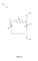
- FIG. 4 is a schematic circuit diagram of the semiconductor device 11 shown in FIG. 2 .
- a circuit 33 comprises the optical avalanche photodiode unit 26 and the thyristor unit 25 coupled to the avalanche photodiode unit 26 by the resistor R1.
- the cathode 28 and the anode 29 are coupled with the thyristor unit 25 through the first and the fourth doped layers 17, 20 (shown in FIG. 2 ) respectively.
- the thyristor unit 25 controls the flow of the electric current from the anode 29 to the cathode 28.
- the incident light 12 is applied to the avalanche photodiode unit 26 to produce a photoinduced current I PHOTO .
- the photoinduced current IPHOTO is amplified to produce an electrical current (not shown), which flows out of the avalanche photodiode unit and functions as a gate current IG (the trigger current) for triggering the thyristor unit 25.
- IG the trigger current
- the thyristor unit 25 and the avalanche photodiode unit 26 are illustrated as being unitary. In other applications, the thyristor unit 25 may be separated from the avalanche photodiode unit 26, and the electric current generated by the avalanche photodiode unit 26 may be directed to the gate terminal of the thyristor unit 25, for example, through an electrical wire.
- the effective circuit 34 for the semiconductor device 11 may comprise more than one thyristor.
- the thyristor unit (not labeled) may comprise a first and a second thyristor 35, 36, which are coupled to the avalanche photodiode unit 26.
- the first (or a switching) thyristor 35 is configured to switch the electric current from the power source 13 to the load 14 (shown in FIG. 1 ).
- the second (or amplifying) thyristor 36 is configured to amplify the electric current from the avalanche photodiode unit 26 and is disposed between the first thyristor 35 and the avalanche photodiode unit 26.
- the first and the second thyristors 35, 36 and the avalanche photodiode unit 26 may be disposed integrally or separately.
- Each of the first and the second thyristor 35, 36 may have a similar configuration as the above-described thyristor unit 25, and include a number of doped wide band-gap semiconductor layers. Typically, the two outer layers of each thyristor 35, 36 are heavily doped layers, while the two inner layers are more lightly doped. Each layer is oppositely doped from the adjacent layer(s). One or both of the inner two layers may act as the gate terminal and be configured to receive the trigger current. Other descriptions of the first and second thyristors 35, 36 can be found, for example, in a U.S Patent Application Ser. No.
- the incident light 12 is applied to the avalanche photodiode unit 26 to produce a photoinduced current I PHOTO .
- the photoinduced current I PHOTO is amplified to produce a first gate current (or a trigger current) I G , flowing to the gate of the second thyristor 36 through the resistor R 1 to activate the second thyristor 36.
- a second gate current (or a second trigger current) I G ' which may be larger than the first gate current I G due to amplification by the second thyristor 36, flows from the second thyristor 36 to the gate of the first thyristor 35 through the resistor R 2 to turn on the first thyristor 35.
- the electric current from the anode 29 can flow through the first thyristor 35 to the cathode 28. This beneficially ensures that the first thyristor 35 can be activated when the first thyristor 35 is used in the high voltage and/or high current applications.
- the optically triggered semiconductor device employs the avalanche photodiode unit to trigger the thyristor unit.
- the trigger current generated is greater, which beneficially extends the applications of the thyristor unit.
- the thyristor unit can also be used in high voltage and/or high current applications. Due to the higher trigger current, the thyristor unit may also be readily triggered.
- the avalanche photodiode unit may be disposed unitarily or separated from the thyristor unit. This beneficially increases the flexibility of the semiconductor device.
- the avalanche photodiode unit and the thyristor unit may be unitary and comprise the common wide band-gap semiconductor body, so that the manufacturing process of such a unitary semiconductor device may be relatively simple, as compared to the manufacturing process of a semiconductor device that which comprises two semiconductor units.
Landscapes
- Thyristors (AREA)
- Light Receiving Elements (AREA)
Applications Claiming Priority (1)
| Application Number | Priority Date | Filing Date | Title |
|---|---|---|---|
| US13/613,848 US9633998B2 (en) | 2012-09-13 | 2012-09-13 | Semiconductor device and method for making the same |
Publications (3)
| Publication Number | Publication Date |
|---|---|
| EP2709154A2 true EP2709154A2 (de) | 2014-03-19 |
| EP2709154A3 EP2709154A3 (de) | 2017-10-18 |
| EP2709154B1 EP2709154B1 (de) | 2020-01-08 |
Family
ID=49123800
Family Applications (1)
| Application Number | Title | Priority Date | Filing Date |
|---|---|---|---|
| EP13184152.0A Active EP2709154B1 (de) | 2012-09-13 | 2013-09-12 | Halbleiterbauelement und Verfahren zu seiner Herstellung |
Country Status (3)
| Country | Link |
|---|---|
| US (1) | US9633998B2 (de) |
| EP (1) | EP2709154B1 (de) |
| JP (1) | JP6306843B2 (de) |
Families Citing this family (3)
| Publication number | Priority date | Publication date | Assignee | Title |
|---|---|---|---|---|
| JP7347005B2 (ja) * | 2019-08-28 | 2023-09-20 | 住友電気工業株式会社 | 受光素子 |
| JP7453615B2 (ja) * | 2020-01-30 | 2024-03-21 | 株式会社Flosfia | 半導体装置および半導体システム |
| CN118198175A (zh) * | 2024-04-03 | 2024-06-14 | 深圳平湖实验室 | 一种光触发晶闸管、晶闸管、其制作方法及电子器件 |
Family Cites Families (34)
| Publication number | Priority date | Publication date | Assignee | Title |
|---|---|---|---|---|
| US3381147A (en) * | 1964-06-02 | 1968-04-30 | Abraham George | Measuring device employing negative resistance |
| JPH0779159B2 (ja) | 1984-03-22 | 1995-08-23 | 潤一 西澤 | 光トリガ・光クエンチ可能なサイリスタ装置 |
| US4572947A (en) * | 1984-05-29 | 1986-02-25 | Westinghouse Electric Corp. | Triggering method for light triggered thyristors |
| JPS62291172A (ja) * | 1986-06-11 | 1987-12-17 | Sharp Corp | 大電力用フオトサイリスタ |
| JPS6384066A (ja) | 1986-09-26 | 1988-04-14 | Semiconductor Res Found | 集積化光トリガ・光クエンチ静電誘導サイリスタ及びその製造方法 |
| JPS63260078A (ja) * | 1987-04-17 | 1988-10-27 | Hitachi Ltd | 過電圧自己保護型サイリスタ |
| US5243205A (en) * | 1989-10-16 | 1993-09-07 | Kabushiki Kaisha Toshiba | Semiconductor device with overvoltage protective function |
| JPH0715005A (ja) * | 1993-06-15 | 1995-01-17 | Hitachi Ltd | 半導体装置及びその製造方法 |
| JP3299374B2 (ja) * | 1994-02-24 | 2002-07-08 | 三菱電機株式会社 | サイリスタ及びその製造方法 |
| FR2727571A1 (fr) * | 1994-11-25 | 1996-05-31 | Sgs Thomson Microelectronics | Thyristor a sensibilite en retournement controlee |
| US5663580A (en) * | 1996-03-15 | 1997-09-02 | Abb Research Ltd. | Optically triggered semiconductor device |
| JP3352349B2 (ja) | 1997-02-24 | 2002-12-03 | シャープ株式会社 | 双方向サイリスタ素子 |
| US6218682B1 (en) | 1997-09-19 | 2001-04-17 | Optiswitch Technology Corporation | Optically controlled thyristor |
| DE50015361D1 (de) * | 1999-02-22 | 2008-10-30 | Infineon Technologies Ag | Verfahren zum einstellen der durchbruchspannung eines thyristors |
| US6525305B2 (en) * | 2000-09-11 | 2003-02-25 | Perkinelmer Canada, Inc. | Large current watchdog circuit for a photodetector |
| US6770911B2 (en) * | 2001-09-12 | 2004-08-03 | Cree, Inc. | Large area silicon carbide devices |
| JP5159023B2 (ja) * | 2002-12-27 | 2013-03-06 | モーメンティブ・パフォーマンス・マテリアルズ・インク | 窒化ガリウム結晶、ホモエピタキシャル窒化ガリウムを基材とするデバイス、及びその製造方法 |
| US7057214B2 (en) * | 2003-07-01 | 2006-06-06 | Optiswitch Technology Corporation | Light-activated semiconductor switches |
| JP4370203B2 (ja) * | 2004-05-25 | 2009-11-25 | 三菱電機株式会社 | 半導体素子 |
| KR101273965B1 (ko) * | 2005-04-22 | 2013-06-12 | 코닌클리케 필립스 일렉트로닉스 엔.브이. | 검출기 픽셀, 방사선 검출기, tof-pet 영상화 시스템, 신틸레이터와 함께 수행되는 방법, 및 의료 영상을 생성하는 방법 |
| US20060261346A1 (en) | 2005-05-18 | 2006-11-23 | Sei-Hyung Ryu | High voltage silicon carbide devices having bi-directional blocking capabilities and methods of fabricating the same |
| US7612340B2 (en) | 2005-08-03 | 2009-11-03 | Drs Sensors & Targeting Systems, Inc. | Method of operating an avalanche photodiode for reducing gain normalized dark current |
| US7582917B2 (en) | 2006-03-10 | 2009-09-01 | Bae Systems Information And Electronic Systems Integration Inc. | Monolithically integrated light-activated thyristor and method |
| CA2623061A1 (en) * | 2007-03-02 | 2008-09-02 | Sean C. Carroll | Zero crossing circuit |
| US20100117188A1 (en) * | 2007-03-05 | 2010-05-13 | General Electric Company | Method for producing trench isolation in silicon carbide and gallium nitride and articles made thereby |
| US8318562B2 (en) * | 2007-04-02 | 2012-11-27 | University Of South Carolina | Method to increase breakdown voltage of semiconductor devices |
| US7989841B1 (en) * | 2007-07-31 | 2011-08-02 | Hewlett-Packard Development Company, L.P. | Fast injection optical switch |
| US20100276699A1 (en) * | 2009-05-04 | 2010-11-04 | University Of South Carolina | Silicon Carbide and Related Wide Bandgap Semiconductor Based Optically-Controlled Power Switching Devices |
| US8796728B2 (en) * | 2010-10-25 | 2014-08-05 | The Board Of Trustees Of The University Of Illinois | Photonically-activated single-bias fast-switching integrated thyristor |
| US8890081B2 (en) * | 2011-04-14 | 2014-11-18 | Los Alamos National Security, Llc. | High-sensitivity, high-speed continuous imaging system |
| WO2014025587A2 (en) * | 2012-08-04 | 2014-02-13 | Applied Physical Electronics, Lc | Apparatus and method for optically initiating collapse of a reverse biased p-type-n-type junction |
| US9069060B1 (en) * | 2013-03-13 | 2015-06-30 | Google Inc. | Circuit architecture for optical receiver with increased dynamic range |
| US9209320B1 (en) * | 2014-08-07 | 2015-12-08 | Omnivision Technologies, Inc. | Method of fabricating a single photon avalanche diode imaging sensor |
| US9685576B2 (en) * | 2014-10-03 | 2017-06-20 | Omnivision Technologies, Inc. | Back side illuminated image sensor with guard ring region reflecting structure |
-
2012
- 2012-09-13 US US13/613,848 patent/US9633998B2/en active Active
-
2013
- 2013-09-10 JP JP2013186876A patent/JP6306843B2/ja active Active
- 2013-09-12 EP EP13184152.0A patent/EP2709154B1/de active Active
Also Published As
| Publication number | Publication date |
|---|---|
| EP2709154A3 (de) | 2017-10-18 |
| JP2014057064A (ja) | 2014-03-27 |
| EP2709154B1 (de) | 2020-01-08 |
| JP6306843B2 (ja) | 2018-04-04 |
| US20140070231A1 (en) | 2014-03-13 |
| US9633998B2 (en) | 2017-04-25 |
Similar Documents
| Publication | Publication Date | Title |
|---|---|---|
| JP5859319B2 (ja) | 半導体素子および逆導通igbt。 | |
| US20160204097A1 (en) | Semiconductor Device Having Overload Current Carrying Capability | |
| CN108630665B (zh) | 功率半导体器件 | |
| KR20070027670A (ko) | 반도체 장치 | |
| NL8001719A (nl) | Tweepolige, op te hoge stroom reagerende beschermingsinrichting. | |
| US20140021508A1 (en) | Thyristor-Based, Dual-Polarity Blocking Photo-Conductive Semiconductor Switch (PCSS) For Short Pulse Switching And Methods | |
| CN111742411B (zh) | 双向晶闸管器件 | |
| EP2709154B1 (de) | Halbleiterbauelement und Verfahren zu seiner Herstellung | |
| US8691634B2 (en) | Optically triggered semiconductor device and method for making the same | |
| JP2005285921A (ja) | アバランシェフォトダイオード | |
| US9748230B2 (en) | Semiconductor apparatus having a trench Schottky barrier Schottky diode | |
| CN110610935B (zh) | 电力电子装置 | |
| US4509089A (en) | Two-pole overcurrent protection device | |
| JP5747581B2 (ja) | 半導体装置 | |
| CN1258381A (zh) | 半导体器件及其应用 | |
| JP3600802B2 (ja) | 限流装置 | |
| CN107112323B (zh) | 集成半导体电路 | |
| CN107845678B (zh) | 功率半导体器件的二极管结构 | |
| US20140145647A1 (en) | Optical Tilted Charge Devices And Techniques | |
| US4951110A (en) | Power semiconductor structural element with four layers | |
| US20120228635A1 (en) | Semiconductor rectifier device | |
| CN116491058B (zh) | 包括可切换旁路器件的模块 | |
| US4536783A (en) | High di/dt, light-triggered thyristor with etched moat current limiting resistors | |
| US6472686B1 (en) | Silicon carbide (SIC) gate turn-off (GTO) thyristor apparatus and method for high power control | |
| US20160284872A1 (en) | Schottky diode |
Legal Events
| Date | Code | Title | Description |
|---|---|---|---|
| PUAI | Public reference made under article 153(3) epc to a published international application that has entered the european phase |
Free format text: ORIGINAL CODE: 0009012 |
|
| AK | Designated contracting states |
Kind code of ref document: A2 Designated state(s): AL AT BE BG CH CY CZ DE DK EE ES FI FR GB GR HR HU IE IS IT LI LT LU LV MC MK MT NL NO PL PT RO RS SE SI SK SM TR |
|
| AX | Request for extension of the european patent |
Extension state: BA ME |
|
| PUAL | Search report despatched |
Free format text: ORIGINAL CODE: 0009013 |
|
| AK | Designated contracting states |
Kind code of ref document: A3 Designated state(s): AL AT BE BG CH CY CZ DE DK EE ES FI FR GB GR HR HU IE IS IT LI LT LU LV MC MK MT NL NO PL PT RO RS SE SI SK SM TR |
|
| AX | Request for extension of the european patent |
Extension state: BA ME |
|
| RIC1 | Information provided on ipc code assigned before grant |
Ipc: H01L 27/08 20060101ALI20170914BHEP Ipc: H01L 29/66 20060101ALI20170914BHEP Ipc: H01L 27/06 20060101AFI20170914BHEP Ipc: H01L 31/111 20060101ALI20170914BHEP |
|
| STAA | Information on the status of an ep patent application or granted ep patent |
Free format text: STATUS: REQUEST FOR EXAMINATION WAS MADE |
|
| 17P | Request for examination filed |
Effective date: 20180418 |
|
| RBV | Designated contracting states (corrected) |
Designated state(s): AL AT BE BG CH CY CZ DE DK EE ES FI FR GB GR HR HU IE IS IT LI LT LU LV MC MK MT NL NO PL PT RO RS SE SI SK SM TR |
|
| RIC1 | Information provided on ipc code assigned before grant |
Ipc: H01L 29/74 20060101ALI20190614BHEP Ipc: H01L 31/111 20060101ALI20190614BHEP Ipc: H01L 29/66 20060101ALI20190614BHEP Ipc: H01L 27/08 20060101ALI20190614BHEP Ipc: H01L 27/06 20060101AFI20190614BHEP Ipc: H01L 27/146 20060101ALI20190614BHEP Ipc: H01L 27/144 20060101ALI20190614BHEP |
|
| GRAP | Despatch of communication of intention to grant a patent |
Free format text: ORIGINAL CODE: EPIDOSNIGR1 |
|
| STAA | Information on the status of an ep patent application or granted ep patent |
Free format text: STATUS: GRANT OF PATENT IS INTENDED |
|
| INTG | Intention to grant announced |
Effective date: 20190805 |
|
| GRAS | Grant fee paid |
Free format text: ORIGINAL CODE: EPIDOSNIGR3 |
|
| GRAA | (expected) grant |
Free format text: ORIGINAL CODE: 0009210 |
|
| STAA | Information on the status of an ep patent application or granted ep patent |
Free format text: STATUS: THE PATENT HAS BEEN GRANTED |
|
| AK | Designated contracting states |
Kind code of ref document: B1 Designated state(s): AL AT BE BG CH CY CZ DE DK EE ES FI FR GB GR HR HU IE IS IT LI LT LU LV MC MK MT NL NO PL PT RO RS SE SI SK SM TR |
|
| REG | Reference to a national code |
Ref country code: GB Ref legal event code: FG4D |
|
| REG | Reference to a national code |
Ref country code: CH Ref legal event code: EP |
|
| REG | Reference to a national code |
Ref country code: DE Ref legal event code: R096 Ref document number: 602013064797 Country of ref document: DE |
|
| REG | Reference to a national code |
Ref country code: IE Ref legal event code: FG4D |
|
| REG | Reference to a national code |
Ref country code: AT Ref legal event code: REF Ref document number: 1223754 Country of ref document: AT Kind code of ref document: T Effective date: 20200215 |
|
| REG | Reference to a national code |
Ref country code: NL Ref legal event code: MP Effective date: 20200108 |
|
| REG | Reference to a national code |
Ref country code: LT Ref legal event code: MG4D |
|
| PG25 | Lapsed in a contracting state [announced via postgrant information from national office to epo] |
Ref country code: NO Free format text: LAPSE BECAUSE OF FAILURE TO SUBMIT A TRANSLATION OF THE DESCRIPTION OR TO PAY THE FEE WITHIN THE PRESCRIBED TIME-LIMIT Effective date: 20200408 Ref country code: RS Free format text: LAPSE BECAUSE OF FAILURE TO SUBMIT A TRANSLATION OF THE DESCRIPTION OR TO PAY THE FEE WITHIN THE PRESCRIBED TIME-LIMIT Effective date: 20200108 Ref country code: FI Free format text: LAPSE BECAUSE OF FAILURE TO SUBMIT A TRANSLATION OF THE DESCRIPTION OR TO PAY THE FEE WITHIN THE PRESCRIBED TIME-LIMIT Effective date: 20200108 Ref country code: PT Free format text: LAPSE BECAUSE OF FAILURE TO SUBMIT A TRANSLATION OF THE DESCRIPTION OR TO PAY THE FEE WITHIN THE PRESCRIBED TIME-LIMIT Effective date: 20200531 Ref country code: NL Free format text: LAPSE BECAUSE OF FAILURE TO SUBMIT A TRANSLATION OF THE DESCRIPTION OR TO PAY THE FEE WITHIN THE PRESCRIBED TIME-LIMIT Effective date: 20200108 Ref country code: LT Free format text: LAPSE BECAUSE OF FAILURE TO SUBMIT A TRANSLATION OF THE DESCRIPTION OR TO PAY THE FEE WITHIN THE PRESCRIBED TIME-LIMIT Effective date: 20200108 |
|
| PG25 | Lapsed in a contracting state [announced via postgrant information from national office to epo] |
Ref country code: GR Free format text: LAPSE BECAUSE OF FAILURE TO SUBMIT A TRANSLATION OF THE DESCRIPTION OR TO PAY THE FEE WITHIN THE PRESCRIBED TIME-LIMIT Effective date: 20200409 Ref country code: IS Free format text: LAPSE BECAUSE OF FAILURE TO SUBMIT A TRANSLATION OF THE DESCRIPTION OR TO PAY THE FEE WITHIN THE PRESCRIBED TIME-LIMIT Effective date: 20200508 Ref country code: BG Free format text: LAPSE BECAUSE OF FAILURE TO SUBMIT A TRANSLATION OF THE DESCRIPTION OR TO PAY THE FEE WITHIN THE PRESCRIBED TIME-LIMIT Effective date: 20200408 Ref country code: SE Free format text: LAPSE BECAUSE OF FAILURE TO SUBMIT A TRANSLATION OF THE DESCRIPTION OR TO PAY THE FEE WITHIN THE PRESCRIBED TIME-LIMIT Effective date: 20200108 Ref country code: LV Free format text: LAPSE BECAUSE OF FAILURE TO SUBMIT A TRANSLATION OF THE DESCRIPTION OR TO PAY THE FEE WITHIN THE PRESCRIBED TIME-LIMIT Effective date: 20200108 Ref country code: HR Free format text: LAPSE BECAUSE OF FAILURE TO SUBMIT A TRANSLATION OF THE DESCRIPTION OR TO PAY THE FEE WITHIN THE PRESCRIBED TIME-LIMIT Effective date: 20200108 |
|
| REG | Reference to a national code |
Ref country code: DE Ref legal event code: R097 Ref document number: 602013064797 Country of ref document: DE |
|
| PG25 | Lapsed in a contracting state [announced via postgrant information from national office to epo] |
Ref country code: ES Free format text: LAPSE BECAUSE OF FAILURE TO SUBMIT A TRANSLATION OF THE DESCRIPTION OR TO PAY THE FEE WITHIN THE PRESCRIBED TIME-LIMIT Effective date: 20200108 Ref country code: DK Free format text: LAPSE BECAUSE OF FAILURE TO SUBMIT A TRANSLATION OF THE DESCRIPTION OR TO PAY THE FEE WITHIN THE PRESCRIBED TIME-LIMIT Effective date: 20200108 Ref country code: SK Free format text: LAPSE BECAUSE OF FAILURE TO SUBMIT A TRANSLATION OF THE DESCRIPTION OR TO PAY THE FEE WITHIN THE PRESCRIBED TIME-LIMIT Effective date: 20200108 Ref country code: EE Free format text: LAPSE BECAUSE OF FAILURE TO SUBMIT A TRANSLATION OF THE DESCRIPTION OR TO PAY THE FEE WITHIN THE PRESCRIBED TIME-LIMIT Effective date: 20200108 Ref country code: SM Free format text: LAPSE BECAUSE OF FAILURE TO SUBMIT A TRANSLATION OF THE DESCRIPTION OR TO PAY THE FEE WITHIN THE PRESCRIBED TIME-LIMIT Effective date: 20200108 Ref country code: CZ Free format text: LAPSE BECAUSE OF FAILURE TO SUBMIT A TRANSLATION OF THE DESCRIPTION OR TO PAY THE FEE WITHIN THE PRESCRIBED TIME-LIMIT Effective date: 20200108 Ref country code: RO Free format text: LAPSE BECAUSE OF FAILURE TO SUBMIT A TRANSLATION OF THE DESCRIPTION OR TO PAY THE FEE WITHIN THE PRESCRIBED TIME-LIMIT Effective date: 20200108 |
|
| PLBE | No opposition filed within time limit |
Free format text: ORIGINAL CODE: 0009261 |
|
| STAA | Information on the status of an ep patent application or granted ep patent |
Free format text: STATUS: NO OPPOSITION FILED WITHIN TIME LIMIT |
|
| REG | Reference to a national code |
Ref country code: AT Ref legal event code: MK05 Ref document number: 1223754 Country of ref document: AT Kind code of ref document: T Effective date: 20200108 |
|
| 26N | No opposition filed |
Effective date: 20201009 |
|
| PG25 | Lapsed in a contracting state [announced via postgrant information from national office to epo] |
Ref country code: IT Free format text: LAPSE BECAUSE OF FAILURE TO SUBMIT A TRANSLATION OF THE DESCRIPTION OR TO PAY THE FEE WITHIN THE PRESCRIBED TIME-LIMIT Effective date: 20200108 Ref country code: AT Free format text: LAPSE BECAUSE OF FAILURE TO SUBMIT A TRANSLATION OF THE DESCRIPTION OR TO PAY THE FEE WITHIN THE PRESCRIBED TIME-LIMIT Effective date: 20200108 |
|
| PG25 | Lapsed in a contracting state [announced via postgrant information from national office to epo] |
Ref country code: PL Free format text: LAPSE BECAUSE OF FAILURE TO SUBMIT A TRANSLATION OF THE DESCRIPTION OR TO PAY THE FEE WITHIN THE PRESCRIBED TIME-LIMIT Effective date: 20200108 Ref country code: SI Free format text: LAPSE BECAUSE OF FAILURE TO SUBMIT A TRANSLATION OF THE DESCRIPTION OR TO PAY THE FEE WITHIN THE PRESCRIBED TIME-LIMIT Effective date: 20200108 |
|
| PG25 | Lapsed in a contracting state [announced via postgrant information from national office to epo] |
Ref country code: MC Free format text: LAPSE BECAUSE OF FAILURE TO SUBMIT A TRANSLATION OF THE DESCRIPTION OR TO PAY THE FEE WITHIN THE PRESCRIBED TIME-LIMIT Effective date: 20200108 |
|
| REG | Reference to a national code |
Ref country code: CH Ref legal event code: PL |
|
| GBPC | Gb: european patent ceased through non-payment of renewal fee |
Effective date: 20200912 |
|
| REG | Reference to a national code |
Ref country code: BE Ref legal event code: MM Effective date: 20200930 |
|
| PG25 | Lapsed in a contracting state [announced via postgrant information from national office to epo] |
Ref country code: LU Free format text: LAPSE BECAUSE OF NON-PAYMENT OF DUE FEES Effective date: 20200912 |
|
| PG25 | Lapsed in a contracting state [announced via postgrant information from national office to epo] |
Ref country code: FR Free format text: LAPSE BECAUSE OF NON-PAYMENT OF DUE FEES Effective date: 20200930 |
|
| PG25 | Lapsed in a contracting state [announced via postgrant information from national office to epo] |
Ref country code: IE Free format text: LAPSE BECAUSE OF NON-PAYMENT OF DUE FEES Effective date: 20200912 Ref country code: GB Free format text: LAPSE BECAUSE OF NON-PAYMENT OF DUE FEES Effective date: 20200912 Ref country code: LI Free format text: LAPSE BECAUSE OF NON-PAYMENT OF DUE FEES Effective date: 20200930 Ref country code: CH Free format text: LAPSE BECAUSE OF NON-PAYMENT OF DUE FEES Effective date: 20200930 Ref country code: BE Free format text: LAPSE BECAUSE OF NON-PAYMENT OF DUE FEES Effective date: 20200930 |
|
| PG25 | Lapsed in a contracting state [announced via postgrant information from national office to epo] |
Ref country code: TR Free format text: LAPSE BECAUSE OF FAILURE TO SUBMIT A TRANSLATION OF THE DESCRIPTION OR TO PAY THE FEE WITHIN THE PRESCRIBED TIME-LIMIT Effective date: 20200108 Ref country code: MT Free format text: LAPSE BECAUSE OF FAILURE TO SUBMIT A TRANSLATION OF THE DESCRIPTION OR TO PAY THE FEE WITHIN THE PRESCRIBED TIME-LIMIT Effective date: 20200108 Ref country code: CY Free format text: LAPSE BECAUSE OF FAILURE TO SUBMIT A TRANSLATION OF THE DESCRIPTION OR TO PAY THE FEE WITHIN THE PRESCRIBED TIME-LIMIT Effective date: 20200108 |
|
| PG25 | Lapsed in a contracting state [announced via postgrant information from national office to epo] |
Ref country code: MK Free format text: LAPSE BECAUSE OF FAILURE TO SUBMIT A TRANSLATION OF THE DESCRIPTION OR TO PAY THE FEE WITHIN THE PRESCRIBED TIME-LIMIT Effective date: 20200108 Ref country code: AL Free format text: LAPSE BECAUSE OF FAILURE TO SUBMIT A TRANSLATION OF THE DESCRIPTION OR TO PAY THE FEE WITHIN THE PRESCRIBED TIME-LIMIT Effective date: 20200108 |
|
| P01 | Opt-out of the competence of the unified patent court (upc) registered |
Effective date: 20230414 |
|
| REG | Reference to a national code |
Ref country code: DE Ref legal event code: R079 Ref document number: 602013064797 Country of ref document: DE Free format text: PREVIOUS MAIN CLASS: H01L0027060000 Ipc: H10D0084000000 |
|
| PGFP | Annual fee paid to national office [announced via postgrant information from national office to epo] |
Ref country code: DE Payment date: 20250820 Year of fee payment: 13 |