EP2708925B1 - Light source device - Google Patents
Light source device Download PDFInfo
- Publication number
- EP2708925B1 EP2708925B1 EP13194373.0A EP13194373A EP2708925B1 EP 2708925 B1 EP2708925 B1 EP 2708925B1 EP 13194373 A EP13194373 A EP 13194373A EP 2708925 B1 EP2708925 B1 EP 2708925B1
- Authority
- EP
- European Patent Office
- Prior art keywords
- light
- light source
- guide plate
- fluorescent material
- light guide
- Prior art date
- Legal status (The legal status is an assumption and is not a legal conclusion. Google has not performed a legal analysis and makes no representation as to the accuracy of the status listed.)
- Active
Links
Images


Classifications
-
- G—PHYSICS
- G02—OPTICS
- G02B—OPTICAL ELEMENTS, SYSTEMS OR APPARATUS
- G02B6/00—Light guides; Structural details of arrangements comprising light guides and other optical elements, e.g. couplings
- G02B6/0001—Light guides; Structural details of arrangements comprising light guides and other optical elements, e.g. couplings specially adapted for lighting devices or systems
- G02B6/0011—Light guides; Structural details of arrangements comprising light guides and other optical elements, e.g. couplings specially adapted for lighting devices or systems the light guides being planar or of plate-like form
- G02B6/0013—Means for improving the coupling-in of light from the light source into the light guide
- G02B6/0023—Means for improving the coupling-in of light from the light source into the light guide provided by one optical element, or plurality thereof, placed between the light guide and the light source, or around the light source
-
- G—PHYSICS
- G02—OPTICS
- G02B—OPTICAL ELEMENTS, SYSTEMS OR APPARATUS
- G02B6/00—Light guides; Structural details of arrangements comprising light guides and other optical elements, e.g. couplings
- G02B6/0001—Light guides; Structural details of arrangements comprising light guides and other optical elements, e.g. couplings specially adapted for lighting devices or systems
- G02B6/0011—Light guides; Structural details of arrangements comprising light guides and other optical elements, e.g. couplings specially adapted for lighting devices or systems the light guides being planar or of plate-like form
- G02B6/0075—Arrangements of multiple light guides
- G02B6/0076—Stacked arrangements of multiple light guides of the same or different cross-sectional area
-
- G—PHYSICS
- G02—OPTICS
- G02B—OPTICAL ELEMENTS, SYSTEMS OR APPARATUS
- G02B6/00—Light guides; Structural details of arrangements comprising light guides and other optical elements, e.g. couplings
- G02B6/0001—Light guides; Structural details of arrangements comprising light guides and other optical elements, e.g. couplings specially adapted for lighting devices or systems
- G02B6/0011—Light guides; Structural details of arrangements comprising light guides and other optical elements, e.g. couplings specially adapted for lighting devices or systems the light guides being planar or of plate-like form
- G02B6/0033—Means for improving the coupling-out of light from the light guide
- G02B6/0035—Means for improving the coupling-out of light from the light guide provided on the surface of the light guide or in the bulk of it
-
- G—PHYSICS
- G02—OPTICS
- G02B—OPTICAL ELEMENTS, SYSTEMS OR APPARATUS
- G02B6/00—Light guides; Structural details of arrangements comprising light guides and other optical elements, e.g. couplings
- G02B6/0001—Light guides; Structural details of arrangements comprising light guides and other optical elements, e.g. couplings specially adapted for lighting devices or systems
- G02B6/0011—Light guides; Structural details of arrangements comprising light guides and other optical elements, e.g. couplings specially adapted for lighting devices or systems the light guides being planar or of plate-like form
- G02B6/0066—Light guides; Structural details of arrangements comprising light guides and other optical elements, e.g. couplings specially adapted for lighting devices or systems the light guides being planar or of plate-like form characterised by the light source being coupled to the light guide
- G02B6/0073—Light emitting diode [LED]
Definitions
- This embodiment relates to a light source device.
- an electric bulb or a fluorescent lamp is commonly used as an indoor or outdoor lighting lamp.
- the electric bulb or the fluorescent lamp has a short life span, so that it should be frequently changed.
- a conventional fluorescent lamp is degraded due to elapse of time for its use. As a result, it is often that its illuminance is gradually decreased.
- the LED is easy to control and has a rapid response speed, high electro-optic conversion efficiency, a long life span, low power consumption and high luminance.
- the LED is also used to create emotional lighting.
- LED lighting is next generation lighting. Since the LED lighting uses a semiconductor device and light with a longer wavelength than that of an ultraviolet ray, it is not harmful to human body.
- WO 2008/060469 relates to LEDs that are connected in series between a first node and a second node, wherein a series current flows between the nodes when an operating voltage is applied across the nodes.
- document WO 2008/152561 relates to light sources that are arranged in a first array and in a second array provided in groups configured to have different beam shaping characteristics.
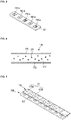
- Fig. 1 is a perspective view showing a light source device according to an embodiment of the present invention.
- Fig. 2 is a view showing a light source unit of the light source device according to the embodiment of the present invention.
- Fig. 3 is a view showing an arrangement structure of light emitting devices of the light source unit according to the embodiment of the present invention.
- Fig. 4 is a view showing a structure of a phosphor luminescent film according to the embodiment of the present invention.
- a light source device 100 includes a light guide plate 110, a reflector 130, a light source unit 150, a photo luminescent film 170, and a diffusing film 190.
- the light guide plate 110 converts a point light source into a surface light source.
- a pattern 111 is formed on one side of the light guide plate 110 such that light incident on the inside of the light guide plate 110 is emitted to the outside.
- the pattern 111 functions to diffuse or scatter the light and to emit to the outside.
- Such a light guide plate 110 may be made of a transparent resin and may be printed by a silk screen printing method and the like.
- the diffuser film 190 is disposed on the light guide plate 110.
- the diffuser film 190 functions to allow the light incident into the inside of the light guide plate 110 to be uniformly emitted to the outside.
- the reflector 130 is disposed under the light guide plate 110.
- the reflector 130 prevents the light incident into the inside of the light guide plate 110 from being emitted to the rear of the light guide plate.
- the light source unit 150 is disposed on the side of the light guide plate 110.
- a light emitting device is used as the light source unit.
- the light source unit 150 is optically coupled to the light guide plate 110, so that light generated from the light source unit 150 is incident into the inside of the light guide plate 110.
- the light source unit 150 includes a printed circuit board 151 and a plurality of light emitting devices 152 disposed on the printed circuit board 151.
- the plurality of the light emitting devices 152 are arranged in a line in the longitudinal direction of the printed circuit board.
- the plurality of the light emitting devices 152 may consist of a blue light emitting device, it is desirable that a white light emitting device with a high colour rendering index (CRI) should be used as the plurality of the light emitting devices 152 if possible.
- the white light emitting device is formed by molding plastic including a yellow fluorescent material on a blue light emitting chip, and creates white light.
- the plastic may include a silicon resin or an epoxy resin.
- the white light emitting device may further include a green fluorescent material or a red fluorescent material so as to increase the colour rendering index (CRI). That is, plastic including a yellow fluorescent material is mainly molded on the blue light emitting chip, and the green fluorescent material and the red fluorescent material may be included in the plastic in the order listed.
- the fluorescent material may include at least one of a garnet based material, a silicate based material, a nitride based material and an oxynitride based material.
- the garnet based material may include YAG (Y 3 Al 5 O 12 :Ce 3+ ) material or TAG (Tb 3 Al 5 O 12 :Ce 3+ ) material.
- the silicate based material may include (Sr, Ba, Mg, Ca) 2 SiO 4 :Eu 2+ material.
- the nitride based material may include CaAlSiN 3 :Eu 2+ material.
- the oxynitride based material may include Si 6-x Al x OxN 8-x :Eu 2+ material.
- the yellow, green and red fluorescent materials included in the plastic when the ratio of the yellow fluorescent material is the highest and the ratio of the red fluorescent material is the lowest, the yellow, green and red fluorescent materials may include a garnet based material, a silicate based material and a nitride based material respectively.
- the yellow, green and red fluorescent materials may include a silicate based material, a silicate based material and a nitride based material respectively.
- the yellow, green and red fluorescent materials may include a garnet based material, an oxynitride based material and a nitride based material respectively.
- the yellow, green and red fluorescent materials may include an oxynitride based material, an oxynitride based material and a nitride based material respectively.
- the plurality of the light emitting devices 152 are comprised of a warm white LED 152-a and a cool white LED 152-b.
- the warm white LED 152-a and the cool white LED 152-b are alternately arranged on the printed circuit board 151. Accordingly, when light is emitted in the form of a surface light source, uniformly mixed light can be emitted from an entire light emitting surface.
- the warm white LED and the cool white LED may be arranged locally or randomly with the order of the LEDs on the printed circuit board.
- the warm white LED 152-a emits a correlated colour temperature within a range between 2,000 K and 3,000 K, and has warm colours.
- the cool white LED 152-b emits a correlated colour temperature within a range between 5,500 K and 6,500 K, and has cool colours.
- the warm white LED 152-a and the cool white LED 152-b per se can emit white light without a combination of a red, green and blue light emitting devices. That is, the warm white LED 152-a and the cool white LED 152-b are formed by molding plastic on the blue light emitting chip.
- the plastic includes a fluorescent material allowing the warm and cool white LEDs 152-a and 152-b to emit light with their corresponding correlated colour temperatures. As a result, correlated colour temperatures for white light can be emitted.
- the warm white LED 152-a and the cool white LED 152-b emit the correlated colour temperatures respectively and emit mixed white light
- the colour rendering index (CRI) representing a degree of being close to natural sunlight becomes higher. Therefore, an actual colour of an object can be prevented from being distorted and the fatigue of the eyes of users is reduced.
- the photo luminescent film 170 is disposed between the light guide plate 110 and the light source unit 150, and includes various fluorescent materials within the photo luminescent film 170.
- the photo luminescent film 170 changes a part of a wavelength of light emitted from the light source unit 150, and changes the colour of the light.
- the photo luminescent film 170 includes a transparent resin 171 and a fluorescent material 172 included within the transparent resin 171.
- the fluorescent material may include at least one of a garnet based material, a silicate based material, a nitride based material and an oxynitride based material.
- the garnet based material may include YAG (Y 3 Al 5 O 12 :Ce 3+ ) material or TAG (Tb 3 Al 5 O 12 :Ce 3+ ) material.
- the silicate based material may include (Sr, Ba, Mg, Ca) 2 SiO 4 :Eu 2+ material.
- the nitride based material may include CaAlSiN 3 :Eu 2+ material.
- the oxynitride based material may include Si 6-x Al x OxN 8-x :Eu 2+ material.
- a transparent protective film 173 is stacked on the transparent resin.
- a silicon resin is mainly used as the transparent resin. Any material having transparency can be used as the transparent resin.
- a curing agent or an additive agent may be included within the transparent resin.
- the curing agent cures the transparent resin.
- the additive agent disperses uniformly the fluorescent material within the transparent resin.
- a diffusing agent may be included within the transparent resin. The diffusing agent improves the refractive index of a light source, thus increasing the excitation ratio of the fluorescent material.
- the transparent protective film 173 disposed on the transparent resin obtains humidity resistance and thermal resistance of the fluorescent material.
- the transparent protective film 173 is made of colourless and transparent plastic having high optical transmittance.
- the transparent protective film 173 may be made of polyethylene terephthalate (PET), polyethylene naphthalate), acrylic resin, polycarbonate and polystyrene and the like.
- Fig. 5 is a view showing an arrangement structure of a fluorescent material included in the phosphor luminescent film according to the embodiment of the present invention and showing a structure in which the phosphor luminescent film and the light source unit are arranged.
- the transparent resin 171 of the photo luminescent film 170 includes a first area and a second area.
- the first area includes a first fluorescent material 172a.
- the second area includes a second fluorescent material 172b different from the first fluorescent material 172a.
- the first fluorescent material 172a and the second fluorescent material 172b are partitioned from each other in the photo luminescent film 170.
- a fluorescent material included in one of the first area and the second area is different from a fluorescent material included in the other area.
- the first area and the second area partitioned in the photo luminescent film 170 are alternately arranged in the longitudinal direction of the photo luminescent film 170.
- the first fluorescent material 172a and the second fluorescent material 172b may be arranged locally or randomly in the longitudinal direction of the photo luminescent film 170.
- the colours of the light is uniformly mixed. As a result, various colours of the light can be created on the entire light emitting surface.
- the colour of light may be created depending on the colour of the light emitted from a light emitting device per se. However, it is preferable that the colour of light is created depending on the fluorescent material included in the photo luminescent film.
- the plurality of the light emitting devices 152 of the light source unit 150 are, as shown, disposed corresponding respectively to the first fluorescent material 172a and the second fluorescent material 172b which are disposed within the photo luminescent film 170. Therefore, alignment characteristic between the plurality of the light emitting devices and the fluorescent materials is satisfactory, thus emitting light having a desired colour temperature.
- the alignment characteristic between the plurality of the light emitting devices and the fluorescent materials does not affect the characteristic of the desired colour.
- the plurality of the light emitting devices are, for example, comprised of the warm white LED and the cool white LED, and when the warm white LED and the cool white LED are alternately arranged, the alignment characteristic between the fluorescent material and the cool and warm white LEDs may deteriorate.
- the alignment characteristic deteriorates, light of an adjacent cool or warm white LED may pass through the fluorescent material.
- Each of the first fluorescent material 172a and the second fluorescent material 172b absorbs light having a specific wavelength and being emitted from the light source unit and converts the light into light having another wavelength. Accordingly, with respect to light emitted outward, it is possible to control the first fluorescent material 172a and the second fluorescent material 172b in accordance with a desired colour of light.
- the fluorescent material included in the photo luminescent film can change the colour of emitted light, thereby creating light having various colours
- the light source device substantially reduces the number of the photo luminescent film and the number of the light guide plate, and reduces manufacturing cost.
- the light source device also prevents the volume of the light source device from being increased by the number of the light guide plate. As a result, a lighting device to which the light source device is applied becomes thinner.
- This embodiment of the present invention includes the shortest optical path. Therefore, a luminous efficiency of this embodiment is improved.
- Fig. 6 is a perspective view showing another light source device according to an embodiment of the present invention.
- Fig. 7 is a view showing a pattern arrangement of a light guide plate according to the embodiment of the present invention.
- Fig. 8 is a view showing a light source unit of the light source device according to the embodiment of the present invention.
- a light source device 100 includes a first light guide plate 110, a second light guide plate 120, a reflector 130, a first light source unit 150, a second light source unit 160, a first photo luminescent film 170 and a second photo luminescent film 180.
- the first light guide plate 110 and the second light guide plate 120 convert a point light source into a surface light source.
- a first pattern 111 and a second pattern 121 are formed on one sides of the light guide plate 110 and the second light guide plate 120 respectively such that light internally incident is emitted to the outside.
- the first light guide plate 110 is stacked on the second light guide plate 120.
- the first pattern 111 and the second pattern 121 which are formed in the first light guide plate 110 and the second light guide plate 120 respectively, function to diffuse or scatter the light and to emit to the outside.
- the first pattern 111 and the second pattern 121 may be disposed such that they are superposed on each other or overlapped with each other.
- first pattern 111 and the second pattern 121 are formed not to be overlapped with each other on one sides of the first light guide plate 110 and the second light guide plate 120 respectively.
- the first pattern 111 and the second pattern 121 are formed in such a manner mentioned above, so that the characteristic of diffusion or scatter of incident light can be improved. As a result, the optical path is reduced and luminous efficiency is enhanced.
- the first light guide plate 110 and the second light guide plate 120 may be made of a transparent resin, and may be printed by a silk screen printing method.
- a diffusing film 190 is disposed on the first light guide plate 110.
- the diffuser film 190 functions to allow the light incident into the insides of the light guide plate 110 and the second light guide plate 120 to be uniformly emitted to the outside.
- the reflector 130 is disposed under the second light guide plate 120.
- the reflector 130 prevents the light incident into the inside of the first light guide plate 110 or the second light guide plate 120 from being emitted to the rears of the light guide plates.
- the first light source unit 150 is disposed on the side of the first light guide plate 110.
- the second light source unit 160 is disposed on the side of the second light guide plate 120. Any device capable of emitting light can be used as the first light guide plate 110 and the second light guide plate 120. In the embodiment of the present invention, a light emitting diode which is one of light emitting devices is used as the light source unit.
- the first light source unit 150 and the second light source unit 160 are optically coupled to the first light guide plate 110 and the second light guide plate 120 respectively, so that light generated from the first light source unit 150 is incident on the first light guide plate 110 and light generated from the second light source unit 160 is incident on the second light guide plate 120.
- the first light source unit 150 and the second light source unit 160 respectively include, as shown in Fig. 8 , printed circuit boards 151 and 161, and a plurality of light emitting devices 152 and 162.
- the plurality of light emitting devices 152 and 162 are disposed on the printed circuit boards 151 and 161 respectively.
- the plurality of the light emitting devices 152 and 162 are arranged in a line in the longitudinal direction of the printed circuit board.
- a light emitting device capable of creating white light has various types according to colour temperatures.
- the plurality of the light emitting device 152 included in the first light source unit 150 are constituted by warm white LEDs and are arranged on the printed circuit board 151.
- the plurality of the light emitting device 162 included in the second light source unit 160 are constituted by cool white LEDs and are arranged on the printed circuit board 161.
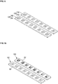
- Fig, 9b is a view showing an embodiment of the present invention, that is, arrangement structures of warm white LEDs and cool white LEDs which are included in a first light source unit and a second light source unit respectively.
- the warm white LEDs may be arranged in a line on the print circuit board 151 of the first light source unit 150.
- the cool white LEDs may be arranged in a line on the print circuit board 161 of the second light source unit 160.
- the warm white LEDs and the cool white LEDs are alternately arranged in a line on the printed circuit board 151 of the first light source unit 150 in a line in the longitudinal direction of the printed circuit board 151.
- the warm white LEDs and the cool white LEDs are also alternately arranged in a line on the printed circuit board 161 of the second light source unit 160 in a line in the longitudinal direction of the printed circuit board 161.
- the warm white LEDs and the cool white LEDs of the first light source unit 150 and the second light source unit 160 are arranged in a grid pattern.
- the warm white LEDs and the cool white LEDs may be randomly arranged all over both the first light source unit 150 and the entire second light source unit 160.
- the first photo luminescent film 170 is disposed between the first light guide plate 110 and the first light source unit 150.
- the second photo luminescent film 180 is disposed between the second light guide plate 120 and the second light source unit 160.
- the first photo luminescent film 170 and the second photo luminescent film 180 include various fluorescent materials thereinside.
- the first photo luminescent film 170 changes a part of a wavelength of light emitted from the first light source unit 150, and changes the colour of the light.
- the second photo luminescent film 180 changes a part of wavelength of light emitted from the second light source unit 160, and changes the colour of the light.
- Fig. 10 is a view showing a structure of a phosphor luminescent film according to the embodiment of the present invention.
- the photo luminescent films 170 and 180 include a transparent resin 171 and a fluorescent material 172 included within the transparent resin 171.
- a transparent protective film 173 is stacked on the transparent resin.
- a silicon resin is mainly used as the transparent resin. Any material having transparency can be used as the transparent resin.
- Fig. 11 is a view showing an arrangement structure of a fluorescent material included in the phosphor luminescent film according to the embodiment of the present invention and showing a structure in which the phosphor luminescent film and the light source unit are arranged.
- the first photo luminescent film 170 includes a first fluorescent material 172a and a second fluorescent material 172b different from the first fluorescent material 172a.
- the first fluorescent material 172a and the second fluorescent material 172b are partitioned from each other in the first photo luminescent film 170, and are alternately arranged in the longitudinal direction of the photo luminescent film 170.
- the second photo luminescent film 180 includes a first fluorescent material 182a and a second fluorescent material 182b different from the first fluorescent material 182a.
- the first fluorescent material 182a and the second fluorescent material 182b are partitioned from each other in the second photo luminescent film 180, and are alternately arranged in the longitudinal direction of the second photo luminescent film 180.
- the first fluorescent materials 172a and 182a and the second fluorescent materials 182a and 182b which are included in both the first photo luminescent film 170 and the second photo luminescent film 180 are arranged in a grid pattern.
- the first fluorescent materials 172a and 182a and the second fluorescent materials 182a and 182b which are included in both the first photo luminescent film 170 and the second photo luminescent film 180 may be locally or randomly arranged in the longitudinal direction of the first photo luminescent film 170 and the second photo luminescent film 180.
- the colours of the light is more uniformly mixed.
- various colours of the light can be created on the entire light emitting surface.
- the colour of light may be created depending on the colour of the light emitted from a light emitting device per se. However, it is preferable that the colour of light is created depending on the fluorescent material included in the photo luminescent film.
- the plurality of the light emitting devices 152 of the light source unit 150 are, as shown, disposed corresponding respectively to the first fluorescent material 172a and second fluorescent material 172b which are disposed within the photo luminescent films 170.
- the plurality of the light emitting devices 162 of the light source unit 160 are, as shown, disposed corresponding respectively to the first fluorescent material 182a and second fluorescent material 182b which are disposed within the photo luminescent films 180. Therefore, alignment characteristic between the plurality of the light emitting devices and the fluorescent materials is satisfactory, thus emitting light having a desired 2. colour temperature.
- the first fluorescent materials 172a and 182a and the second fluorescent materials 172b and 182b absorb respectively light having a specific wavelength and being emitted from the light source units 150 and 160 and convert the light into light having another wavelength. Accordingly, with respect to light emitted outward, it is possible to control the first fluorescent materials 172a and 182a and the second fluorescent materials 172b and 182b in accordance with a desired colour of light.
- the fluorescent material included in the photo luminescent film can change the colour of emitted light, thereby creating light having various colours.
Landscapes
- Physics & Mathematics (AREA)
- General Physics & Mathematics (AREA)
- Optics & Photonics (AREA)
- Planar Illumination Modules (AREA)
- Optical Elements Other Than Lenses (AREA)
- Led Device Packages (AREA)
Applications Claiming Priority (3)
| Application Number | Priority Date | Filing Date | Title |
|---|---|---|---|
| KR1020100033040A KR101720305B1 (ko) | 2010-04-10 | 2010-04-10 | 광원 장치 |
| KR1020100033039A KR101652818B1 (ko) | 2010-04-10 | 2010-04-10 | 광원 장치 |
| EP11153485.5A EP2378322B1 (en) | 2010-04-10 | 2011-02-07 | Light source device |
Related Parent Applications (1)
| Application Number | Title | Priority Date | Filing Date |
|---|---|---|---|
| EP11153485.5A Division EP2378322B1 (en) | 2010-04-10 | 2011-02-07 | Light source device |
Publications (2)
| Publication Number | Publication Date |
|---|---|
| EP2708925A1 EP2708925A1 (en) | 2014-03-19 |
| EP2708925B1 true EP2708925B1 (en) | 2022-03-30 |
Family
ID=44168117
Family Applications (2)
| Application Number | Title | Priority Date | Filing Date |
|---|---|---|---|
| EP11153485.5A Not-in-force EP2378322B1 (en) | 2010-04-10 | 2011-02-07 | Light source device |
| EP13194373.0A Active EP2708925B1 (en) | 2010-04-10 | 2011-02-07 | Light source device |
Family Applications Before (1)
| Application Number | Title | Priority Date | Filing Date |
|---|---|---|---|
| EP11153485.5A Not-in-force EP2378322B1 (en) | 2010-04-10 | 2011-02-07 | Light source device |
Country Status (4)
| Country | Link |
|---|---|
| US (1) | US9541695B2 (enExample) |
| EP (2) | EP2378322B1 (enExample) |
| JP (1) | JP5736218B2 (enExample) |
| CN (1) | CN102252274B (enExample) |
Families Citing this family (18)
| Publication number | Priority date | Publication date | Assignee | Title |
|---|---|---|---|---|
| TW201243239A (en) * | 2011-03-17 | 2012-11-01 | Rambus Inc | Lighting assembly with adjustable light output |
| KR101881333B1 (ko) * | 2011-08-31 | 2018-07-25 | 엘지이노텍 주식회사 | 조명 모듈 |
| DE102012105445A1 (de) * | 2012-06-22 | 2013-12-24 | Osram Opto Semiconductors Gmbh | Flächenlichtquelle |
| FR3000783B1 (fr) * | 2013-01-08 | 2015-03-06 | Commissariat Energie Atomique | Structure photo-active, procede de fabrication d'une telle structure et systeme d'eclairage |
| EP2765175A3 (en) * | 2013-02-07 | 2014-09-03 | Everlight Electronics Co., Ltd | Phosphor compositions for highly reliable white light-emitting diode devices |
| JP6265055B2 (ja) | 2014-01-14 | 2018-01-24 | ソニー株式会社 | 発光装置、表示装置および照明装置 |
| KR20150093283A (ko) | 2014-02-06 | 2015-08-18 | 삼성디스플레이 주식회사 | 프레임 및 이를 포함하는 광원모듈 |
| DE202014103047U1 (de) * | 2014-03-27 | 2014-08-20 | Tridonic Jennersdorf Gmbh | Beleuchtungsvorrichtung zur Erzeugung von weißem Licht |
| DE102015114910A1 (de) * | 2014-09-19 | 2016-03-24 | Ford Global Technologies, Llc | Photolumineszierende Fahrzeugstufenleuchte |
| CN107429885A (zh) * | 2015-03-10 | 2017-12-01 | 夏普株式会社 | 照明装置、显示装置以及电视接收装置 |
| US9974138B2 (en) | 2015-04-21 | 2018-05-15 | GE Lighting Solutions, LLC | Multi-channel lamp system and method with mixed spectrum |
| CN104879706A (zh) * | 2015-06-01 | 2015-09-02 | 上海向隆电子科技有限公司 | 导光板灯具 |
| KR102430999B1 (ko) | 2015-06-24 | 2022-08-10 | 쑤저우 레킨 세미컨덕터 컴퍼니 리미티드 | 광원 모듈 |
| CN105700235A (zh) * | 2016-04-13 | 2016-06-22 | 京东方科技集团股份有限公司 | 一种背光模组及显示装置 |
| JP6963183B2 (ja) * | 2018-06-22 | 2021-11-05 | 日亜化学工業株式会社 | 発光モジュールの製造方法 |
| DE202020100855U1 (de) * | 2020-02-18 | 2021-05-25 | Zumtobel Lighting Gmbh | Flächenleuchte mit direkter und indirekter Lichtabgabe |
| JP7731026B2 (ja) * | 2021-07-08 | 2025-08-29 | 株式会社Magnolia White | 照明装置 |
| TWI841043B (zh) * | 2022-11-10 | 2024-05-01 | 元太科技工業股份有限公司 | 光源裝置及反射式顯示器 |
Citations (2)
| Publication number | Priority date | Publication date | Assignee | Title |
|---|---|---|---|---|
| US20070215890A1 (en) * | 2006-03-17 | 2007-09-20 | Philips Lumileds Lighting Company, Llc | White LED for backlight with phosphor plates |
| WO2008152561A1 (en) * | 2007-06-14 | 2008-12-18 | Koninklijke Philips Electronics N.V. | Led-based luminaire with adjustable beam shape |
Family Cites Families (44)
| Publication number | Priority date | Publication date | Assignee | Title |
|---|---|---|---|---|
| US5506929A (en) * | 1994-10-19 | 1996-04-09 | Clio Technologies, Inc. | Light expanding system for producing a linear or planar light beam from a point-like light source |
| JP3937644B2 (ja) * | 1999-03-25 | 2007-06-27 | セイコーエプソン株式会社 | 光源及び照明装置並びにその照明装置を用いた液晶装置 |
| JP2004031023A (ja) | 2002-06-24 | 2004-01-29 | Kyocera Corp | バックライト、液晶表示装置および表示機器 |
| US7178941B2 (en) * | 2003-05-05 | 2007-02-20 | Color Kinetics Incorporated | Lighting methods and systems |
| CN1981157B (zh) * | 2004-05-05 | 2011-03-16 | 伦斯勒工业学院 | 使用固态发射器和降频转换材料的高效光源 |
| US7213958B2 (en) * | 2004-06-30 | 2007-05-08 | 3M Innovative Properties Company | Phosphor based illumination system having light guide and an interference reflector |
| US7256057B2 (en) * | 2004-09-11 | 2007-08-14 | 3M Innovative Properties Company | Methods for producing phosphor based light sources |
| TWI254821B (en) | 2004-10-01 | 2006-05-11 | Delta Electronics Inc | Backlight module |
| US8125137B2 (en) * | 2005-01-10 | 2012-02-28 | Cree, Inc. | Multi-chip light emitting device lamps for providing high-CRI warm white light and light fixtures including the same |
| US20060268537A1 (en) * | 2005-05-31 | 2006-11-30 | Makoto Kurihara | Phosphor film, lighting device using the same, and display device |
| JP4579065B2 (ja) | 2005-06-23 | 2010-11-10 | セイコーインスツル株式会社 | 照明装置、及びこれを備える表示装置 |
| JP4469307B2 (ja) * | 2005-05-31 | 2010-05-26 | セイコーインスツル株式会社 | 表示装置 |
| US7891852B2 (en) * | 2005-10-17 | 2011-02-22 | Koninklijke Philips Electronics Nv | Illumination system using phosphor remote from light source |
| WO2007074787A1 (ja) * | 2005-12-27 | 2007-07-05 | Matsushita Electric Industrial Co., Ltd. | 面状照明装置とそれを用いた液晶表示装置 |
| JP2007265716A (ja) | 2006-03-28 | 2007-10-11 | Matsushita Electric Ind Co Ltd | 面状光源及び液晶表示装置 |
| US7365991B2 (en) * | 2006-04-14 | 2008-04-29 | Renaissance Lighting | Dual LED board layout for lighting systems |
| US20070263409A1 (en) * | 2006-05-09 | 2007-11-15 | Mok Thye L | Light guide plate with reflective light mixing |
| KR101318034B1 (ko) * | 2006-08-22 | 2013-10-14 | 엘지디스플레이 주식회사 | 광학 유닛, 이를 갖는 백라이트 어셈블리 및 이를 갖는표시장치 |
| JP2008116849A (ja) * | 2006-11-07 | 2008-05-22 | Sony Corp | 表示装置 |
| DE602007007804D1 (de) * | 2006-11-10 | 2010-08-26 | Philips Solid State Lighting | Verfahren und vorrichtung zur steuerung von hintereinandergeschalteten led |
| US8172415B2 (en) * | 2007-05-24 | 2012-05-08 | Koninklijke Philips Electronics N.V. | Color-tunable illumination system |
| WO2009011922A1 (en) * | 2007-07-18 | 2009-01-22 | Qd Vision, Inc. | Quantum dot-based light sheets useful for solid-state lighting |
| KR100915465B1 (ko) | 2007-09-28 | 2009-09-04 | (주) 이지닉스 | 광원 장치 |
| US7984999B2 (en) * | 2007-10-17 | 2011-07-26 | Xicato, Inc. | Illumination device with light emitting diodes and moveable light adjustment member |
| US7915627B2 (en) * | 2007-10-17 | 2011-03-29 | Intematix Corporation | Light emitting device with phosphor wavelength conversion |
| US7845826B2 (en) * | 2008-01-15 | 2010-12-07 | Skc Haas Display Films Co., Ltd. | Multilayered integrated backlight illumination assembly |
| JP2009211819A (ja) | 2008-02-29 | 2009-09-17 | Effect Meiji:Kk | ディスプレイ用照明装置 |
| US8016443B2 (en) * | 2008-05-02 | 2011-09-13 | Light Prescriptions Innovators, Llc | Remote-phosphor LED downlight |
| CN102017204A (zh) * | 2008-05-07 | 2011-04-13 | 皇家飞利浦电子股份有限公司 | 具有包含发光材料的自支撑网格的led照明器件和制作自支撑网格的方法 |
| US9074751B2 (en) * | 2008-06-20 | 2015-07-07 | Seoul Semiconductor Co., Ltd. | Lighting apparatus |
| WO2009157352A1 (ja) * | 2008-06-23 | 2009-12-30 | ソニー株式会社 | 面光源装置および表示装置 |
| WO2010002226A2 (ko) * | 2008-07-03 | 2010-01-07 | 삼성엘이디 주식회사 | Led 패키지 및 그 led 패키지를 포함하는 백라이트 유닛 |
| US8427605B2 (en) * | 2008-09-23 | 2013-04-23 | Koninklijke Philips Electronics N.V. | Illumination device with electrical variable scattering element |
| US8277085B2 (en) * | 2008-10-06 | 2012-10-02 | Light Prescriptions Innovators, Llc | Compact LED downlight with cuspated flux-redistribution lens |
| US20110242433A1 (en) * | 2008-10-27 | 2011-10-06 | Sharp Kabushiki Kaisha | Lighting device, display device and television receiver |
| US7762704B2 (en) * | 2008-11-19 | 2010-07-27 | Bryter Technologies LLC | Optimized distribution of light extraction from an edge lit light source |
| CN101749654A (zh) * | 2008-12-18 | 2010-06-23 | 富士迈半导体精密工业(上海)有限公司 | 照明装置 |
| US20100157406A1 (en) * | 2008-12-19 | 2010-06-24 | Qualcomm Mems Technologies, Inc. | System and method for matching light source emission to display element reflectivity |
| JP2012517106A (ja) * | 2009-02-04 | 2012-07-26 | リンデール インコーポレイテッド | 蛍光体複合物を被覆した拡散デバイスおよび方法 |
| JP4399678B1 (ja) | 2009-02-12 | 2010-01-20 | 鈴木 優一 | 照明装置および表示装置 |
| US7967652B2 (en) * | 2009-02-19 | 2011-06-28 | Cree, Inc. | Methods for combining light emitting devices in a package and packages including combined light emitting devices |
| JP5143770B2 (ja) * | 2009-03-02 | 2013-02-13 | 株式会社ジャパンディスプレイイースト | 液晶表示装置 |
| US7985000B2 (en) * | 2009-04-08 | 2011-07-26 | Ledengin, Inc. | Lighting apparatus having multiple light-emitting diodes with individual light-conversion layers |
| US8764224B2 (en) * | 2010-08-12 | 2014-07-01 | Cree, Inc. | Luminaire with distributed LED sources |
-
2011
- 2011-02-07 EP EP11153485.5A patent/EP2378322B1/en not_active Not-in-force
- 2011-02-07 EP EP13194373.0A patent/EP2708925B1/en active Active
- 2011-03-04 US US13/040,444 patent/US9541695B2/en not_active Expired - Fee Related
- 2011-03-29 CN CN201110082385.7A patent/CN102252274B/zh not_active Expired - Fee Related
- 2011-04-01 JP JP2011081409A patent/JP5736218B2/ja not_active Expired - Fee Related
Patent Citations (2)
| Publication number | Priority date | Publication date | Assignee | Title |
|---|---|---|---|---|
| US20070215890A1 (en) * | 2006-03-17 | 2007-09-20 | Philips Lumileds Lighting Company, Llc | White LED for backlight with phosphor plates |
| WO2008152561A1 (en) * | 2007-06-14 | 2008-12-18 | Koninklijke Philips Electronics N.V. | Led-based luminaire with adjustable beam shape |
Also Published As
| Publication number | Publication date |
|---|---|
| EP2378322A1 (en) | 2011-10-19 |
| EP2708925A1 (en) | 2014-03-19 |
| JP2011222506A (ja) | 2011-11-04 |
| CN102252274B (zh) | 2014-09-24 |
| US20110205727A1 (en) | 2011-08-25 |
| CN102252274A (zh) | 2011-11-23 |
| US9541695B2 (en) | 2017-01-10 |
| EP2378322B1 (en) | 2014-01-08 |
| JP5736218B2 (ja) | 2015-06-17 |
Similar Documents
| Publication | Publication Date | Title |
|---|---|---|
| EP2708925B1 (en) | Light source device | |
| JP6083931B2 (ja) | 照明モジュール | |
| US20120140436A1 (en) | Solid-state lamps with light guide and photoluminescence material | |
| JP2012531047A (ja) | Led型ランプおよび光放出サイネージ | |
| JP5200067B2 (ja) | 発光装置 | |
| JP2011159970A (ja) | 発光素子パッケージ | |
| JP2011040313A (ja) | 中空導光ユニット、面光源および液晶ディスプレイ | |
| US20140191273A1 (en) | Light-emitting arrangement | |
| JP2022525050A (ja) | 照明モジュール及びこれを備えた照明装置 | |
| CN103765080B (zh) | 照明模块 | |
| KR101652818B1 (ko) | 광원 장치 | |
| KR101720305B1 (ko) | 광원 장치 | |
| KR20200126290A (ko) | 조명 모듈 및 이를 구비한 조명 장치 | |
| KR101827712B1 (ko) | 조명 모듈 | |
| KR102400249B1 (ko) | 발광 모듈 및 이를 포함하는 디스플레이 장치 | |
| KR101827709B1 (ko) | 조명 모듈 | |
| KR101894080B1 (ko) | 조명 모듈 | |
| KR102897298B1 (ko) | 조명장치 | |
| KR102856401B1 (ko) | 조명 장치 | |
| KR101765902B1 (ko) | 발광장치 | |
| KR20080057656A (ko) | 평판형 조명 장치 | |
| KR101839868B1 (ko) | 조명 모듈 | |
| KR20120131998A (ko) | 조명 모듈 | |
| KR20120131999A (ko) | 조명 모듈 | |
| KR20130024309A (ko) | 조명 모듈 |
Legal Events
| Date | Code | Title | Description |
|---|---|---|---|
| PUAI | Public reference made under article 153(3) epc to a published international application that has entered the european phase |
Free format text: ORIGINAL CODE: 0009012 |
|
| AC | Divisional application: reference to earlier application |
Ref document number: 2378322 Country of ref document: EP Kind code of ref document: P |
|
| AK | Designated contracting states |
Kind code of ref document: A1 Designated state(s): AL AT BE BG CH CY CZ DE DK EE ES FI FR GB GR HR HU IE IS IT LI LT LU LV MC MK MT NL NO PL PT RO RS SE SI SK SM TR |
|
| 17P | Request for examination filed |
Effective date: 20140331 |
|
| RAP1 | Party data changed (applicant data changed or rights of an application transferred) |
Owner name: LG INNOTEK CO., LTD. |
|
| RBV | Designated contracting states (corrected) |
Designated state(s): AL AT BE BG CH CY CZ DE DK EE ES FI FR GB GR HR HU IE IS IT LI LT LU LV MC MK MT NL NO PL PT RO RS SE SI SK SM TR |
|
| RAP1 | Party data changed (applicant data changed or rights of an application transferred) |
Owner name: LG INNOTEK CO., LTD. |
|
| STAA | Information on the status of an ep patent application or granted ep patent |
Free format text: STATUS: EXAMINATION IS IN PROGRESS |
|
| 17Q | First examination report despatched |
Effective date: 20181114 |
|
| RAP1 | Party data changed (applicant data changed or rights of an application transferred) |
Owner name: SUZHOU LEKIN SEMICONDUCTOR CO., LTD. |
|
| GRAP | Despatch of communication of intention to grant a patent |
Free format text: ORIGINAL CODE: EPIDOSNIGR1 |
|
| STAA | Information on the status of an ep patent application or granted ep patent |
Free format text: STATUS: GRANT OF PATENT IS INTENDED |
|
| INTG | Intention to grant announced |
Effective date: 20211022 |
|
| GRAS | Grant fee paid |
Free format text: ORIGINAL CODE: EPIDOSNIGR3 |
|
| GRAA | (expected) grant |
Free format text: ORIGINAL CODE: 0009210 |
|
| STAA | Information on the status of an ep patent application or granted ep patent |
Free format text: STATUS: THE PATENT HAS BEEN GRANTED |
|
| AC | Divisional application: reference to earlier application |
Ref document number: 2378322 Country of ref document: EP Kind code of ref document: P |
|
| AK | Designated contracting states |
Kind code of ref document: B1 Designated state(s): AL AT BE BG CH CY CZ DE DK EE ES FI FR GB GR HR HU IE IS IT LI LT LU LV MC MK MT NL NO PL PT RO RS SE SI SK SM TR |
|
| REG | Reference to a national code |
Ref country code: GB Ref legal event code: FG4D |
|
| REG | Reference to a national code |
Ref country code: CH Ref legal event code: EP |
|
| REG | Reference to a national code |
Ref country code: AT Ref legal event code: REF Ref document number: 1479734 Country of ref document: AT Kind code of ref document: T Effective date: 20220415 |
|
| REG | Reference to a national code |
Ref country code: DE Ref legal event code: R096 Ref document number: 602011072690 Country of ref document: DE |
|
| REG | Reference to a national code |
Ref country code: IE Ref legal event code: FG4D |
|
| REG | Reference to a national code |
Ref country code: LT Ref legal event code: MG9D |
|
| PG25 | Lapsed in a contracting state [announced via postgrant information from national office to epo] |
Ref country code: SE Free format text: LAPSE BECAUSE OF FAILURE TO SUBMIT A TRANSLATION OF THE DESCRIPTION OR TO PAY THE FEE WITHIN THE PRESCRIBED TIME-LIMIT Effective date: 20220330 Ref country code: RS Free format text: LAPSE BECAUSE OF FAILURE TO SUBMIT A TRANSLATION OF THE DESCRIPTION OR TO PAY THE FEE WITHIN THE PRESCRIBED TIME-LIMIT Effective date: 20220330 Ref country code: NO Free format text: LAPSE BECAUSE OF FAILURE TO SUBMIT A TRANSLATION OF THE DESCRIPTION OR TO PAY THE FEE WITHIN THE PRESCRIBED TIME-LIMIT Effective date: 20220630 Ref country code: LT Free format text: LAPSE BECAUSE OF FAILURE TO SUBMIT A TRANSLATION OF THE DESCRIPTION OR TO PAY THE FEE WITHIN THE PRESCRIBED TIME-LIMIT Effective date: 20220330 Ref country code: HR Free format text: LAPSE BECAUSE OF FAILURE TO SUBMIT A TRANSLATION OF THE DESCRIPTION OR TO PAY THE FEE WITHIN THE PRESCRIBED TIME-LIMIT Effective date: 20220330 Ref country code: BG Free format text: LAPSE BECAUSE OF FAILURE TO SUBMIT A TRANSLATION OF THE DESCRIPTION OR TO PAY THE FEE WITHIN THE PRESCRIBED TIME-LIMIT Effective date: 20220630 |
|
| REG | Reference to a national code |
Ref country code: NL Ref legal event code: MP Effective date: 20220330 |
|
| REG | Reference to a national code |
Ref country code: AT Ref legal event code: MK05 Ref document number: 1479734 Country of ref document: AT Kind code of ref document: T Effective date: 20220330 |
|
| PG25 | Lapsed in a contracting state [announced via postgrant information from national office to epo] |
Ref country code: LV Free format text: LAPSE BECAUSE OF FAILURE TO SUBMIT A TRANSLATION OF THE DESCRIPTION OR TO PAY THE FEE WITHIN THE PRESCRIBED TIME-LIMIT Effective date: 20220330 Ref country code: GR Free format text: LAPSE BECAUSE OF FAILURE TO SUBMIT A TRANSLATION OF THE DESCRIPTION OR TO PAY THE FEE WITHIN THE PRESCRIBED TIME-LIMIT Effective date: 20220701 Ref country code: FI Free format text: LAPSE BECAUSE OF FAILURE TO SUBMIT A TRANSLATION OF THE DESCRIPTION OR TO PAY THE FEE WITHIN THE PRESCRIBED TIME-LIMIT Effective date: 20220330 |
|
| PG25 | Lapsed in a contracting state [announced via postgrant information from national office to epo] |
Ref country code: NL Free format text: LAPSE BECAUSE OF FAILURE TO SUBMIT A TRANSLATION OF THE DESCRIPTION OR TO PAY THE FEE WITHIN THE PRESCRIBED TIME-LIMIT Effective date: 20220330 |
|
| PG25 | Lapsed in a contracting state [announced via postgrant information from national office to epo] |
Ref country code: SM Free format text: LAPSE BECAUSE OF FAILURE TO SUBMIT A TRANSLATION OF THE DESCRIPTION OR TO PAY THE FEE WITHIN THE PRESCRIBED TIME-LIMIT Effective date: 20220330 Ref country code: SK Free format text: LAPSE BECAUSE OF FAILURE TO SUBMIT A TRANSLATION OF THE DESCRIPTION OR TO PAY THE FEE WITHIN THE PRESCRIBED TIME-LIMIT Effective date: 20220330 Ref country code: RO Free format text: LAPSE BECAUSE OF FAILURE TO SUBMIT A TRANSLATION OF THE DESCRIPTION OR TO PAY THE FEE WITHIN THE PRESCRIBED TIME-LIMIT Effective date: 20220330 Ref country code: PT Free format text: LAPSE BECAUSE OF FAILURE TO SUBMIT A TRANSLATION OF THE DESCRIPTION OR TO PAY THE FEE WITHIN THE PRESCRIBED TIME-LIMIT Effective date: 20220801 Ref country code: ES Free format text: LAPSE BECAUSE OF FAILURE TO SUBMIT A TRANSLATION OF THE DESCRIPTION OR TO PAY THE FEE WITHIN THE PRESCRIBED TIME-LIMIT Effective date: 20220330 Ref country code: EE Free format text: LAPSE BECAUSE OF FAILURE TO SUBMIT A TRANSLATION OF THE DESCRIPTION OR TO PAY THE FEE WITHIN THE PRESCRIBED TIME-LIMIT Effective date: 20220330 Ref country code: CZ Free format text: LAPSE BECAUSE OF FAILURE TO SUBMIT A TRANSLATION OF THE DESCRIPTION OR TO PAY THE FEE WITHIN THE PRESCRIBED TIME-LIMIT Effective date: 20220330 Ref country code: AT Free format text: LAPSE BECAUSE OF FAILURE TO SUBMIT A TRANSLATION OF THE DESCRIPTION OR TO PAY THE FEE WITHIN THE PRESCRIBED TIME-LIMIT Effective date: 20220330 |
|
| PG25 | Lapsed in a contracting state [announced via postgrant information from national office to epo] |
Ref country code: PL Free format text: LAPSE BECAUSE OF FAILURE TO SUBMIT A TRANSLATION OF THE DESCRIPTION OR TO PAY THE FEE WITHIN THE PRESCRIBED TIME-LIMIT Effective date: 20220330 Ref country code: IS Free format text: LAPSE BECAUSE OF FAILURE TO SUBMIT A TRANSLATION OF THE DESCRIPTION OR TO PAY THE FEE WITHIN THE PRESCRIBED TIME-LIMIT Effective date: 20220730 Ref country code: AL Free format text: LAPSE BECAUSE OF FAILURE TO SUBMIT A TRANSLATION OF THE DESCRIPTION OR TO PAY THE FEE WITHIN THE PRESCRIBED TIME-LIMIT Effective date: 20220330 |
|
| REG | Reference to a national code |
Ref country code: DE Ref legal event code: R097 Ref document number: 602011072690 Country of ref document: DE |
|
| PG25 | Lapsed in a contracting state [announced via postgrant information from national office to epo] |
Ref country code: DK Free format text: LAPSE BECAUSE OF FAILURE TO SUBMIT A TRANSLATION OF THE DESCRIPTION OR TO PAY THE FEE WITHIN THE PRESCRIBED TIME-LIMIT Effective date: 20220330 |
|
| PLBE | No opposition filed within time limit |
Free format text: ORIGINAL CODE: 0009261 |
|
| STAA | Information on the status of an ep patent application or granted ep patent |
Free format text: STATUS: NO OPPOSITION FILED WITHIN TIME LIMIT |
|
| 26N | No opposition filed |
Effective date: 20230103 |
|
| PGFP | Annual fee paid to national office [announced via postgrant information from national office to epo] |
Ref country code: FR Payment date: 20230110 Year of fee payment: 13 |
|
| PG25 | Lapsed in a contracting state [announced via postgrant information from national office to epo] |
Ref country code: SI Free format text: LAPSE BECAUSE OF FAILURE TO SUBMIT A TRANSLATION OF THE DESCRIPTION OR TO PAY THE FEE WITHIN THE PRESCRIBED TIME-LIMIT Effective date: 20220330 |
|
| PGFP | Annual fee paid to national office [announced via postgrant information from national office to epo] |
Ref country code: GB Payment date: 20230105 Year of fee payment: 13 Ref country code: DE Payment date: 20230104 Year of fee payment: 13 |
|
| PG25 | Lapsed in a contracting state [announced via postgrant information from national office to epo] |
Ref country code: IT Free format text: LAPSE BECAUSE OF FAILURE TO SUBMIT A TRANSLATION OF THE DESCRIPTION OR TO PAY THE FEE WITHIN THE PRESCRIBED TIME-LIMIT Effective date: 20220330 |
|
| PG25 | Lapsed in a contracting state [announced via postgrant information from national office to epo] |
Ref country code: MC Free format text: LAPSE BECAUSE OF FAILURE TO SUBMIT A TRANSLATION OF THE DESCRIPTION OR TO PAY THE FEE WITHIN THE PRESCRIBED TIME-LIMIT Effective date: 20220330 |
|
| REG | Reference to a national code |
Ref country code: CH Ref legal event code: PL |
|
| REG | Reference to a national code |
Ref country code: BE Ref legal event code: MM Effective date: 20230228 |
|
| PG25 | Lapsed in a contracting state [announced via postgrant information from national office to epo] |
Ref country code: LU Free format text: LAPSE BECAUSE OF NON-PAYMENT OF DUE FEES Effective date: 20230207 Ref country code: LI Free format text: LAPSE BECAUSE OF NON-PAYMENT OF DUE FEES Effective date: 20230228 Ref country code: CH Free format text: LAPSE BECAUSE OF NON-PAYMENT OF DUE FEES Effective date: 20230228 |
|
| REG | Reference to a national code |
Ref country code: IE Ref legal event code: MM4A |
|
| PG25 | Lapsed in a contracting state [announced via postgrant information from national office to epo] |
Ref country code: IE Free format text: LAPSE BECAUSE OF NON-PAYMENT OF DUE FEES Effective date: 20230207 |
|
| PG25 | Lapsed in a contracting state [announced via postgrant information from national office to epo] |
Ref country code: BE Free format text: LAPSE BECAUSE OF NON-PAYMENT OF DUE FEES Effective date: 20230228 |
|
| REG | Reference to a national code |
Ref country code: DE Ref legal event code: R119 Ref document number: 602011072690 Country of ref document: DE |
|
| GBPC | Gb: european patent ceased through non-payment of renewal fee |
Effective date: 20240207 |
|
| PG25 | Lapsed in a contracting state [announced via postgrant information from national office to epo] |
Ref country code: DE Free format text: LAPSE BECAUSE OF NON-PAYMENT OF DUE FEES Effective date: 20240903 |
|
| PG25 | Lapsed in a contracting state [announced via postgrant information from national office to epo] |
Ref country code: GB Free format text: LAPSE BECAUSE OF NON-PAYMENT OF DUE FEES Effective date: 20240207 |
|
| PG25 | Lapsed in a contracting state [announced via postgrant information from national office to epo] |
Ref country code: FR Free format text: LAPSE BECAUSE OF NON-PAYMENT OF DUE FEES Effective date: 20240229 |
|
| PG25 | Lapsed in a contracting state [announced via postgrant information from national office to epo] |
Ref country code: GB Free format text: LAPSE BECAUSE OF NON-PAYMENT OF DUE FEES Effective date: 20240207 Ref country code: FR Free format text: LAPSE BECAUSE OF NON-PAYMENT OF DUE FEES Effective date: 20240229 Ref country code: DE Free format text: LAPSE BECAUSE OF NON-PAYMENT OF DUE FEES Effective date: 20240903 |
|
| PG25 | Lapsed in a contracting state [announced via postgrant information from national office to epo] |
Ref country code: CY Free format text: LAPSE BECAUSE OF FAILURE TO SUBMIT A TRANSLATION OF THE DESCRIPTION OR TO PAY THE FEE WITHIN THE PRESCRIBED TIME-LIMIT; INVALID AB INITIO Effective date: 20110207 |
|
| PG25 | Lapsed in a contracting state [announced via postgrant information from national office to epo] |
Ref country code: HU Free format text: LAPSE BECAUSE OF FAILURE TO SUBMIT A TRANSLATION OF THE DESCRIPTION OR TO PAY THE FEE WITHIN THE PRESCRIBED TIME-LIMIT; INVALID AB INITIO Effective date: 20110207 |
|
| PG25 | Lapsed in a contracting state [announced via postgrant information from national office to epo] |
Ref country code: TR Free format text: LAPSE BECAUSE OF FAILURE TO SUBMIT A TRANSLATION OF THE DESCRIPTION OR TO PAY THE FEE WITHIN THE PRESCRIBED TIME-LIMIT Effective date: 20220330 |