EP2378322B1 - Light source device - Google Patents
Light source device Download PDFInfo
- Publication number
- EP2378322B1 EP2378322B1 EP11153485.5A EP11153485A EP2378322B1 EP 2378322 B1 EP2378322 B1 EP 2378322B1 EP 11153485 A EP11153485 A EP 11153485A EP 2378322 B1 EP2378322 B1 EP 2378322B1
- Authority
- EP
- European Patent Office
- Prior art keywords
- light source
- light
- fluorescent material
- guide plate
- source unit
- Prior art date
- Legal status (The legal status is an assumption and is not a legal conclusion. Google has not performed a legal analysis and makes no representation as to the accuracy of the status listed.)
- Active
Links
- 239000000463 material Substances 0.000 claims description 146
- 239000011347 resin Substances 0.000 claims description 24
- 229920005989 resin Polymers 0.000 claims description 24
- 150000004767 nitrides Chemical class 0.000 claims description 9
- BPQQTUXANYXVAA-UHFFFAOYSA-N Orthosilicate Chemical compound [O-][Si]([O-])([O-])[O-] BPQQTUXANYXVAA-UHFFFAOYSA-N 0.000 claims description 8
- 239000003795 chemical substances by application Substances 0.000 claims description 7
- 230000002596 correlated effect Effects 0.000 claims description 7
- 239000002223 garnet Substances 0.000 claims description 7
- 230000001681 protective effect Effects 0.000 claims description 7
- 230000000875 corresponding effect Effects 0.000 claims description 5
- OAICVXFJPJFONN-UHFFFAOYSA-N Phosphorus Chemical class [P] OAICVXFJPJFONN-UHFFFAOYSA-N 0.000 description 12
- 239000003086 colorant Substances 0.000 description 10
- 229920003023 plastic Polymers 0.000 description 8
- 239000004033 plastic Substances 0.000 description 7
- 230000003287 optical effect Effects 0.000 description 5
- 238000009877 rendering Methods 0.000 description 5
- XUIMIQQOPSSXEZ-UHFFFAOYSA-N Silicon Chemical compound [Si] XUIMIQQOPSSXEZ-UHFFFAOYSA-N 0.000 description 3
- 229910052710 silicon Inorganic materials 0.000 description 3
- 239000010703 silicon Substances 0.000 description 3
- 108010043121 Green Fluorescent Proteins Proteins 0.000 description 2
- 239000000654 additive Substances 0.000 description 2
- 230000000996 additive effect Effects 0.000 description 2
- 230000000694 effects Effects 0.000 description 2
- 230000002996 emotional effect Effects 0.000 description 2
- 229910052909 inorganic silicate Inorganic materials 0.000 description 2
- 238000004519 manufacturing process Methods 0.000 description 2
- 238000000034 method Methods 0.000 description 2
- 230000004048 modification Effects 0.000 description 2
- 238000012986 modification Methods 0.000 description 2
- 238000000465 moulding Methods 0.000 description 2
- -1 polyethylene terephthalate Polymers 0.000 description 2
- 229920000139 polyethylene terephthalate Polymers 0.000 description 2
- 239000005020 polyethylene terephthalate Substances 0.000 description 2
- 238000007650 screen-printing Methods 0.000 description 2
- 229910019655 synthetic inorganic crystalline material Inorganic materials 0.000 description 2
- 229910019901 yttrium aluminum garnet Inorganic materials 0.000 description 2
- 239000004925 Acrylic resin Substances 0.000 description 1
- 229920000178 Acrylic resin Polymers 0.000 description 1
- 239000004793 Polystyrene Substances 0.000 description 1
- 238000006243 chemical reaction Methods 0.000 description 1
- 230000003247 decreasing effect Effects 0.000 description 1
- 238000009792 diffusion process Methods 0.000 description 1
- 239000003822 epoxy resin Substances 0.000 description 1
- 230000005284 excitation Effects 0.000 description 1
- 229920003207 poly(ethylene-2,6-naphthalate) Polymers 0.000 description 1
- 239000004417 polycarbonate Substances 0.000 description 1
- 229920000515 polycarbonate Polymers 0.000 description 1
- 229920000647 polyepoxide Polymers 0.000 description 1
- 239000011112 polyethylene naphthalate Substances 0.000 description 1
- 229920002223 polystyrene Polymers 0.000 description 1
- 239000004065 semiconductor Substances 0.000 description 1
- 238000002834 transmittance Methods 0.000 description 1
Images


Classifications
-
- G—PHYSICS
- G02—OPTICS
- G02B—OPTICAL ELEMENTS, SYSTEMS OR APPARATUS
- G02B6/00—Light guides; Structural details of arrangements comprising light guides and other optical elements, e.g. couplings
- G02B6/0001—Light guides; Structural details of arrangements comprising light guides and other optical elements, e.g. couplings specially adapted for lighting devices or systems
- G02B6/0011—Light guides; Structural details of arrangements comprising light guides and other optical elements, e.g. couplings specially adapted for lighting devices or systems the light guides being planar or of plate-like form
- G02B6/0013—Means for improving the coupling-in of light from the light source into the light guide
- G02B6/0023—Means for improving the coupling-in of light from the light source into the light guide provided by one optical element, or plurality thereof, placed between the light guide and the light source, or around the light source
-
- G—PHYSICS
- G02—OPTICS
- G02B—OPTICAL ELEMENTS, SYSTEMS OR APPARATUS
- G02B6/00—Light guides; Structural details of arrangements comprising light guides and other optical elements, e.g. couplings
- G02B6/0001—Light guides; Structural details of arrangements comprising light guides and other optical elements, e.g. couplings specially adapted for lighting devices or systems
- G02B6/0011—Light guides; Structural details of arrangements comprising light guides and other optical elements, e.g. couplings specially adapted for lighting devices or systems the light guides being planar or of plate-like form
- G02B6/0075—Arrangements of multiple light guides
- G02B6/0076—Stacked arrangements of multiple light guides of the same or different cross-sectional area
-
- G—PHYSICS
- G02—OPTICS
- G02B—OPTICAL ELEMENTS, SYSTEMS OR APPARATUS
- G02B6/00—Light guides; Structural details of arrangements comprising light guides and other optical elements, e.g. couplings
- G02B6/0001—Light guides; Structural details of arrangements comprising light guides and other optical elements, e.g. couplings specially adapted for lighting devices or systems
- G02B6/0011—Light guides; Structural details of arrangements comprising light guides and other optical elements, e.g. couplings specially adapted for lighting devices or systems the light guides being planar or of plate-like form
- G02B6/0033—Means for improving the coupling-out of light from the light guide
- G02B6/0035—Means for improving the coupling-out of light from the light guide provided on the surface of the light guide or in the bulk of it
-
- G—PHYSICS
- G02—OPTICS
- G02B—OPTICAL ELEMENTS, SYSTEMS OR APPARATUS
- G02B6/00—Light guides; Structural details of arrangements comprising light guides and other optical elements, e.g. couplings
- G02B6/0001—Light guides; Structural details of arrangements comprising light guides and other optical elements, e.g. couplings specially adapted for lighting devices or systems
- G02B6/0011—Light guides; Structural details of arrangements comprising light guides and other optical elements, e.g. couplings specially adapted for lighting devices or systems the light guides being planar or of plate-like form
- G02B6/0066—Light guides; Structural details of arrangements comprising light guides and other optical elements, e.g. couplings specially adapted for lighting devices or systems the light guides being planar or of plate-like form characterised by the light source being coupled to the light guide
- G02B6/0073—Light emitting diode [LED]
Definitions
- This embodiment relates to a light source device.
- an electric bulb or a fluorescent lamp is commonly used as an indoor or outdoor lighting lamp.
- the electric bulb or the fluorescent lamp has a short life span, so that it should be frequently changed.
- a conventional fluorescent lamp is degraded due to elapse of time for its use. As a result, it is often that its illuminance is gradually decreased.
- the LED is easy to control and has a rapid response speed, high electro-optic conversion efficiency, a long life span, low power consumption and high luminance.
- the LED is also used to create emotional lighting.
- LED lighting is next generation lighting. Since the LED lighting uses a semiconductor device and light with a longer wavelength than that of an ultraviolet ray, it is not harmful to human body.
- a light source device implements a high color rendering property and prevents the color of an object from being distorted.
- a light source device mixes various colors and creates emotional lighting.
- a light source device reduces its the weight and thickness and allows the lighting device to be thinner.
- a light source device reduces the number of its parts, so that manufacturing cost thereof is reduced.
- the light source device includes:
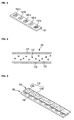
- Fig. 1 is a perspective view showing a light source device according to an embodiment of the present invention.
- Fig. 2 is a view showing a light source unit of the light source device according to the embodiment of the present invention.
- Fig. 3 is a view showing an arrangement structure of light emitting devices of the light source unit according to the embodiment of the present invention.
- Fig. 4 is a view showing a structure of a phosphor luminescent film according to the embodiment of the present invention.
- a light source device 100 includes a light guide plate 110, a reflector 130, a light source unit 150, a photo luminescent film 170, and a diffusing film 190.
- the light guide plate 110 converts a point light source into a surface light source.
- a pattern 111 is formed on one side of the light guide plate 110 such that light incident on the inside of the light guide plate 110 is emitted to the outside.
- the pattern 111 functions to diffuse or scatter the light and to emit to the outside.
- Such a light guide plate 110 may be made of a transparent resin and may be printed by a silk screen printing method and the like.
- the diffuser film 190 is disposed on the light guide plate 110.
- the diffuser film 190 functions to allow the light incident into the inside of the light guide plate 110 to be uniformly emitted to the outside.
- the reflector 130 is disposed under the light guide plate 110.
- the reflector 130 prevents the light incident into the inside of the light guide plate 110 from being emitted to the rear of the light guide plate.
- the light source unit 150 is disposed on the side of the light guide plate 110. Any device capable of emitting light can be used as the light source unit 150. In the embodiment of the present invention, a light emitting device is used as the light source unit.
- the light source unit 150 is optically coupled to the light guide plate 110, so that light generated from the light source unit 150 is incident into the inside of the light guide plate 110.
- the light source unit 150 includes a printed circuit board 151 and a plurality of light emitting devices 152 disposed on the printed circuit board 151.
- the plurality of the light emitting devices 152 are arranged in a line in the longitudinal direction of the printed circuit board.
- the plurality of the light emitting devices 152 may consist of a blue light emitting device, it is desirable that a white light emitting device with a high color rendering index (CRI) should be used as the plurality of the light emitting devices 152 if possible.
- the white light emitting device is formed by molding plastic including a yellow fluorescent material on a blue light emitting chip, and creates white light.
- the plastic may include a silicon resin or an epoxy resin.
- the white light emitting device may further include a green fluorescent material or a red fluorescent material so as to increase the color rendering index (CRI). That is, plastic including a yellow fluorescent material is mainly molded on the blue light emitting chip, and the green fluorescent material and the red fluorescent material may be included in the plastic in the order listed.
- the fluorescent material may include at least one of a garnet based material, a silicate based material, a nitride based material and an oxynitride based material.
- the garnet based material may include YAG (Y 3 Al 5 O 12 :Ce 3+ ) material or TAG (Tb 3 Al 5 O 12 :Ce 3+ ) material.
- the silicate based material may include (Sr, Ba, Mg, Ca) 2 SiO 4 :Eu 2+ material.
- the nitride based material may include CaAlSiN 3 :Eu 2+ material.
- the oxynitride based material may include Si 6-x Al x OxN 8-x :Eu 2+ material.
- the yellow, green and red fluorescent materials included in the plastic when the ratio of the yellow fluorescent material is the highest and the ratio of the red fluorescent material is the lowest, the yellow, green and red fluorescent materials may include a garnet based material, a silicate based material and a nitride based material respectively.
- the yellow, green and red fluorescent materials may include a silicate based material, a silicate based material and a nitride based material respectively.
- the yellow, green and red fluorescent materials may include a garnet based material, an oxynitride based material and a nitride based material respectively.
- the yellow, green and red fluorescent materials may include an oxynitride based material, an oxynitride based material and a nitride based material respectively.
- the plurality of the light emitting devices 152 are comprised of a warm white LED 152-a and a cool white LED 152-b.
- the warm white LED 152-a and the cool white LED 152-b are alternately arranged on the printed circuit board 151. Accordingly, when light is emitted in the form of a surface light source, uniformly mixed light can be emitted from an entire light emitting surface.
- the warm white LED and the cool white LED may be arranged locally or randomly with the order of the LEDs on the printed circuit board.
- the warm white LED 152-a emits a correlated color temperature within a range between 2,000 K and 3,000 K, and has warm colors.
- the cool white LED 152-b emits a correlated color temperature within a range between 5,500 K and 6,500 K, and has cool colors.
- the warm white LED 152-a and the cool white LED 152-b per se can emit white light without a combination of a red, green and blue light emitting devices. That is, the warm white LED 152-a and the cool white LED 152-b are formed by molding plastic on the blue light emitting chip.
- the plastic includes a fluorescent material allowing the warm and cool white LEDs 152-a and 152-b to emit light with their corresponding correlated color temperatures. As a result, correlated color temperatures for white light can be emitted.
- the warm white LED 152-a and the cool white LED 152-b emit the correlated color temperatures respectively and emit mixed white light
- the color rendering index (CRI) representing a degree of being close to natural sunlight becomes higher. Therefore, an actual color of an object can be prevented from being distorted and the fatigue of the eyes of users is reduced.
- the photo luminescent film 170 is disposed between the light guide plate 110 and the light source unit 150, and includes various fluorescent materials within the photo luminescent film 170.
- the photo luminescent film 170 changes a part of a wavelength of light emitted from the light source unit 150, and changes the color of the light.
- the photo luminescent film 170 includes a transparent resin 171 and a fluorescent material 172 included within the transparent resin 171.
- the fluorescent material may include at least one of a garnet based material, a silicate based material, a nitride based material and an oxynitride based material.
- the garnet based material may include YAG(Y 3 Al 5 O 12 :Ce 3+ ) material or TAG (Tb 3 Al 5 O 12 :Ce 3+ ) material.
- the silicate based material may include (Sr, Ba, Mg, Ca) 2 SiO 4 :Eu 2+ material.
- the nitride based material may include CaAlSiN 3 :Eu 2+ material.
- the oxynitride based material may include Si 6-x Al x OxN 8-x :Eu 2+ material.
- a transparent protective film 173 is stacked on the transparent resin.
- a silicon resin is mainly used as the transparent resin. Any material having transparency can be used as the transparent resin.
- a curing agent or an additive agent may be included within the transparent resin.
- the curing agent cures the transparent resin.
- the additive agent disperses uniformly the fluorescent material within the transparent resin.
- a diffusing agent may be included within the transparent resin. The diffusing agent improves the refractive index of a light source, thus increasing the excitation ratio of the fluorescent material.
- the transparent protective film 173 disposed on the transparent resin obtains humidity resistance and thermal resistance of the fluorescent material.
- the transparent protective film 173 is made of colorless and transparent plastic having high optical transmittance.
- the transparent protective film 173 may be made of polyethylene terephthalate (PET), polyethylene naphthalate), acrylic resin, polycarbonate and polystyrene and the like.
- Fig. 5 is a view showing an arrangement structure of a fluorescent material included in the phosphor luminescent film according to the embodiment of the present invention and showing a structure in which the phosphor luminescent film and the light source unit are arranged.
- the transparent resin 171 of the photo luminescent film 170 includes a first area and a second area.
- the first area includes a first fluorescent material 172a.
- the second area includes a second fluorescent material 172b different from the first fluorescent material 172a.
- the first fluorescent material 172a and the second fluorescent material 172b are partitioned from each other in the photo luminescent film 170.
- a fluorescent material included in one of the first area and the second area may be different from a fluorescent material included in the other area.
- the first area and the second area partitioned in the photo luminescent film 170 are alternately arranged in the longitudinal direction of the photo luminescent film 170.
- the first fluorescent material 172a and the second fluorescent material 172b may be arranged locally or randomly in the longitudinal direction of the photo luminescent film 170.
- the colors of the light is uniformly mixed. As a result, various colors of the light can be created on the entire light emitting surface.
- the color of light may be created depending on the color of the light emitted from a light emitting device per se. However, it is preferable that the color of light is created depending on the fluorescent material included in the photo luminescent film.
- the plurality of the light emitting devices 152 of the light source unit 150 are, as shown, disposed corresponding respectively to the first fluorescent material 172a and the second fluorescent material 172b which are disposed within the photo luminescent film 170. Therefore, alignment characteristic between the plurality of the light emitting devices and the fluorescent materials is satisfactory, thus emitting light having a desired color temperature.
- the alignment characteristic between the plurality of the light emitting devices and the fluorescent materials does not affect the characteristic of the desired color.
- the plurality of the light emitting devices are, for example, comprised of the warm white LED and the cool white LED, and when the warm white LED and the cool white LED are alternately arranged, the alignment characteristic between the fluorescent material and the cool and warm white LEDs may deteriorate.
- the alignment characteristic deteriorates, light of an adjacent cool or warm white LED may pass through the fluorescent material. Thus, there occurs a problem that light having an undesired color temperature is emitted.
- Each of the first fluorescent material 172a and the second fluorescent material 172b absorbs light having a specific wavelength and being emitted from the light source unit and converts the light into light having another wavelength. Accordingly, with respect to light emitted outward, it is possible to control the first fluorescent material 172a and the second fluorescent material 172b in accordance with a desired color of light.
- the fluorescent material included in the photo luminescent film can change the color of emitted light, thereby creating light having various colors.
- the light source device substantially reduces the number of the photo luminescent film and the number of the light guide plate, and reduces manufacturing cost.
- the light source device also prevents the volume of the light source device from being increased by the number of the light guide plate. As a result, a lighting device to which the light source device is applied becomes thinner.
- This embodiment of the present invention includes the shortest optical path. Therefore, a luminous efficiency of this embodiment is improved.
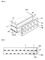
- Fig. 6 is a perspective view showing another light source device according to an embodiment of the present invention.
- Fig. 7 is a view showing a pattern arrangement of a light guide plate according to the embodiment of the present invention.
- Fig. 8 is a view showing a light source unit of the light source device according to the embodiment of the present invention.
- a light source device 100 includes a first light guide plate 110, a second light guide plate 120, a reflector 130, a first light source unit 150, a second light source unit 160, a first photo luminescent film 170 and a second photo luminescent film 180.
- the first light guide plate 110 and the second light guide plate 120 convert a point light source into a surface light source.
- a first pattern 111 and a second pattern 121 are formed on one sides of the light guide plate 110 and the second light guide plate 120 respectively such that light internally incident is emitted to the outside.
- the first light guide plate 110 is stacked on the second light guide plate 120.
- the first pattern 111 and the second pattern 121 which are formed in the first light guide plate 110 and the second light guide plate 120 respectively, function to diffuse or scatter the light and to emit to the outside.
- the first pattern 111 and the second pattern 121 may be disposed such that they are superposed on each other or overlapped with each other. However, it is preferable that the first pattern 111 and the second pattern 121 are formed not to be overlapped with each other on one sides of the first light guide plate 110 and the second light guide plate 120 respectively.
- the first pattern 111 and the second pattern 121 are formed in such a manner mentioned above, so that the characteristic of diffusion or scatter of incident light can be improved. As a result, the optical path is reduced and luminous efficiency is enhanced.
- the first light guide plate 110 and the second light guide plate 120 may be made of a transparent resin, and may be printed by a silk screen printing method.
- a diffusing film 190 is disposed on the first light guide plate 110.
- the diffuser film 190 functions to allow the light incident into the insides of the light guide plate 110 and the second light guide plate 120 to be uniformly emitted to the outside.
- the reflector 130 is disposed under the second light guide plate 120.
- the reflector 130 prevents the light incident into the inside of the first light guide plate 110 or the second light guide plate 120 from being emitted to the rears of the light guide plates.
- the first light source unit 150 is disposed on the side of the first light guide plate 110.
- the second light source unit 160 is disposed on the side of the second light guide plate 120. Any device capable of emitting light can be used as the first light guide plate 110 and the second light guide plate 120. In the embodiment of the present invention, a light emitting diode which is one of light emitting devices is used as the light source unit.
- the first light source unit 150 and the second light source unit 160 are optically coupled to the first light guide plate 110 and the second light guide plate 120 respectively, so that light generated from the first light source unit 150 is incident on the first light guide plate 110 and light generated from the second light source unit 160 is incident on the second light guide plate 120.
- the first light source unit 150 and the second light source unit 160 respectively include, as shown in Fig. 8 , printed circuit boards 151 and 161, and a plurality of light emitting devices 152 and 162.
- the plurality of light emitting devices 152 and 162 are disposed on the printed circuit boards 151 and 161 respectively.
- the plurality of the light emitting devices 152 and 162 are arranged in a line in the longitudinal direction of the printed circuit board.
- a light emitting device capable of creating white light has various types according to color temperatures.
- the plurality of the light emitting device 152 included in the first light source unit 150 are constituted by warm white LEDs and are arranged on the printed circuit board 151.
- the plurality of the light emitting device 162 included in the second light source unit 160 are constituted by cool white LEDs and are arranged on the printed circuit board 161.
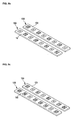
- Figs. 9a to 9c are views showing an embodiment of the present invention, that is, arrangement structures of warm white LEDs and cool white LEDs which are included in a first light source unit and a second light source unit respectively.
- the warm white LEDs may be arranged in a line on the print circuit board 151 of the first light source unit 150.
- the cool white LEDs may be arranged in a line on the print circuit board 161 of the second light source unit 160.
- the warm white LEDs and the cool white LEDs are alternately arranged in a line on the printed circuit board 151 of the first light source unit 150 in a line in the longitudinal direction of the printed circuit board 151.
- the warm white LEDs and the cool white LEDs are also alternately arranged in a line on the printed circuit board 161 of the second light source unit 160 in a line in the longitudinal direction of the printed circuit board 161.
- the warm white LEDs and the cool white LEDs of the first light source unit 150 and the second light source unit 160 are arranged in a grid pattern.
- the warm white LEDs and the cool white LEDs may be randomly arranged all over both the first light source unit 150 and the entire second light source unit 160.
- the first photo luminescent film 170 is disposed between the first light guide plate 110 and the first light source unit 150.
- the second photo luminescent film 180 is disposed between the second light guide plate 120 and the second light source unit 160.
- the first photo luminescent film 170 and the second photo luminescent film 180 include various fluorescent materials thereinside.
- the first photo luminescent film 170 changes a part of a wavelength of light emitted from the first light source unit 150, and changes the color of the light.
- the second photo luminescent film 180 changes a part of wavelength of light emitted from the second light source unit 160, and changes the color of the light.
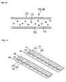
- Fig. 10 is a view showing a structure of a phosphor luminescent film according to the embodiment of the present invention.
- the photo luminescent films 170 and 180 include a transparent resin 171 and a fluorescent material 172 included within the transparent resin 171.
- a transparent protective film 173 is stacked on the transparent resin.
- a silicon resin is mainly used as the transparent resin. Any material having transparency can be used as the transparent resin.
- Fig. 11 is a view showing an arrangement structure of a fluorescent material included in the phosphor luminescent film according to the embodiment of the present invention and showing a structure in which the phosphor luminescent film and the light source unit are arranged.
- the first photo luminescent film 170 includes a first fluorescent material 172a and a second fluorescent material 172b different from the first fluorescent material 172a.
- the first fluorescent material 172a and the second fluorescent material 172b are partitioned from each other in the first photo luminescent film 170, and are alternately arranged in the longitudinal direction of the photo luminescent film 170.
- the second photo luminescent film 180 includes a first fluorescent material 182a and a second fluorescent material 182b different from the first fluorescent material 182a.
- the first fluorescent material 182a and the second fluorescent material 182b are partitioned from each other in the second photo luminescent film 180, and are alternately arranged in the longitudinal direction of the second photo luminescent film 180.
- the first fluorescent materials 172a and 182a and the second fluorescent materials 182a and 182b which are included in both the first photo luminescent film 170 and the second photo luminescent film 180 are arranged in a grid pattern.
- the first fluorescent materials 172a and 182a and the second fluorescent materials 182a and 182b which are included in both the first photo luminescent film 170 and the second photo luminescent film 180 may be locally or randomly arranged in the longitudinal direction of the first photo luminescent film 170 and the second photo luminescent film 180.
- the first fluorescent materials 172a and 182a and the second fluorescent materials 182a and 182b are alternately arranged and when light is emitted to the outside through the light guide plate in the form of a surface light source, the colors of the light is more uniformly mixed. As a result, various colors of the light can be created on the entire light emitting surface.
- the color of light may be created depending on the color of the light emitted from a light emitting device per se. However, it is preferable that the color of light is created depending on the fluorescent material included in the photo luminescent film.
- the plurality of the light emitting devices 152 of the light source unit 150 are, as shown, disposed corresponding respectively to the first fluorescent material 172a and second fluorescent material 172b which are disposed within the photo luminescent films 170.
- the plurality of the light emitting devices 162 of the light source unit 160 are, as shown, disposed corresponding respectively to the first fluorescent material 182a and second fluorescent material 182b which are disposed within the photo luminescent films 180. Therefore, alignment characteristic between the plurality of the light emitting devices and the fluorescent materials is satisfactory, thus emitting light having a desired color temperature.
- the first fluorescent materials 172a and 182a and the second fluorescent materials 172b and 182b absorb respectively light having a specific wavelength and being emitted from the light source units 150 and 160 and convert the light into light having another wavelength. Accordingly, with respect to light emitted outward, it is possible to control the first fluorescent materials 172a and 182a and the second fluorescent materials 172b and 182b in accordance with a desired color of light.
- the fluorescent material included in the photo luminescent film can change the color of emitted light, thereby creating light having various colors.
Description
- This embodiment relates to a light source device.
- In general, an electric bulb or a fluorescent lamp is commonly used as an indoor or outdoor lighting lamp. However, the electric bulb or the fluorescent lamp has a short life span, so that it should be frequently changed. Moreover, a conventional fluorescent lamp is degraded due to elapse of time for its use. As a result, it is often that its illuminance is gradually decreased.
- In order to overcome such problems, a lighting apparatus is now being developed by using a light emitting device (hereinafter, referred to as LED). The LED is easy to control and has a rapid response speed, high electro-optic conversion efficiency, a long life span, low power consumption and high luminance. The LED is also used to create emotional lighting.
- Light emitting device (LED) lighting is next generation lighting. Since the LED lighting uses a semiconductor device and light with a longer wavelength than that of an ultraviolet ray, it is not harmful to human body.
- Therefore, many lighting apparatuses to which the LED is applied are now being developed. However, a lot of parts are required at present to create various colors or a characteristic of light which is a source of lighting, for example, a color rendering index (CRI).
- A light source device according to the embodiment implements a high color rendering property and prevents the color of an object from being distorted.
- A light source device according to the embodiment mixes various colors and creates emotional lighting.
- A light source device according to the embodiment reduces its the weight and thickness and allows the lighting device to be thinner.
- A light source device according to the embodiment reduces the number of its parts, so that manufacturing cost thereof is reduced.
- One aspect of this invention is a light source device. The light source device includes:
- a light guide plate;
- a reflector disposed under the light guide plate;
- a light source unit optically coupled to the light guide plate; and
- a photo luminescent film disposed between the light guide plate and the light source unit, wherein the photo luminescent film comprises at least two partitioned areas, and wherein a first fluorescent material comprised in at least one area of the at least two areas is different from a second fluorescent material comprised in the other areas.
-
-
Fig. 1 is a perspective view showing a light source device according to an embodiment of the present invention. -
Fig. 2 is a view showing a light source unit of the light source device according to the embodiment of the present invention. -
Fig. 3 is a view showing an arrangement structure of light emitting devices of the light source unit according to the embodiment of the present invention. -
Fig. 4 is a view showing a structure of a phosphor luminescent film according to the embodiment of the present invention. -
Fig. 5 is a view showing an arrangement structure of a fluorescent material included in the phosphor luminescent film according to the embodiment of the present invention and showing a structure in which the phosphor luminescent film and the light source unit are arranged. -
Fig. 6 is a perspective view showing another light source device according to an embodiment of the present invention. -
Fig. 7 is a view showing a pattern arrangement of a light guide plate according to the embodiment of the present invention. -
Fig. 8 is a view showing a light source unit of the light source device according to the embodiment of the present invention. -
Figs. 9a to 9c are views showing an embodiment of the present invention, that is, arrangement structures of warm white LEDs and cool white LEDs which are included in a first light source unit and a second light source unit respectively. -
Fig. 10 is a view showing a structure of a phosphor luminescent film according to the embodiment of the present invention. -
Fig. 11 is a view showing an arrangement structure of a fluorescent material included in the phosphor luminescent film according to the embodiment of the present invention and showing a structure in which the phosphor luminescent film and the light source unit are arranged. - It will be understood that when an element is referred to as being 'on' or "under" another element, it can be directly on/under the element, and one or more intervening elements may also be present. When an element is referred to as being 'on' or 'under', 'under the element' as well as 'on the element' can be included based on the element.
- Hereinafter, an embodiment will be described in detail with reference to the accompanying drawings.
-
Fig. 1 is a perspective view showing a light source device according to an embodiment of the present invention.Fig. 2 is a view showing a light source unit of the light source device according to the embodiment of the present invention.Fig. 3 is a view showing an arrangement structure of light emitting devices of the light source unit according to the embodiment of the present invention.Fig. 4 is a view showing a structure of a phosphor luminescent film according to the embodiment of the present invention. - First, referring to
Fig. 1 , alight source device 100 includes alight guide plate 110, areflector 130, alight source unit 150, a photoluminescent film 170, and a diffusingfilm 190. - The
light guide plate 110 converts a point light source into a surface light source. Apattern 111 is formed on one side of thelight guide plate 110 such that light incident on the inside of thelight guide plate 110 is emitted to the outside. Thepattern 111 functions to diffuse or scatter the light and to emit to the outside. Such alight guide plate 110 may be made of a transparent resin and may be printed by a silk screen printing method and the like. - The
diffuser film 190 is disposed on thelight guide plate 110. Thediffuser film 190 functions to allow the light incident into the inside of thelight guide plate 110 to be uniformly emitted to the outside. - The
reflector 130 is disposed under thelight guide plate 110. Thereflector 130 prevents the light incident into the inside of thelight guide plate 110 from being emitted to the rear of the light guide plate. - The
light source unit 150 is disposed on the side of thelight guide plate 110. Any device capable of emitting light can be used as thelight source unit 150. In the embodiment of the present invention, a light emitting device is used as the light source unit. Thelight source unit 150 is optically coupled to thelight guide plate 110, so that light generated from thelight source unit 150 is incident into the inside of thelight guide plate 110. - As shown in
Fig. 2 , thelight source unit 150 includes a printedcircuit board 151 and a plurality oflight emitting devices 152 disposed on the printedcircuit board 151. The plurality of thelight emitting devices 152 are arranged in a line in the longitudinal direction of the printed circuit board. Though the plurality of thelight emitting devices 152 may consist of a blue light emitting device, it is desirable that a white light emitting device with a high color rendering index (CRI) should be used as the plurality of thelight emitting devices 152 if possible. The white light emitting device is formed by molding plastic including a yellow fluorescent material on a blue light emitting chip, and creates white light. Here, the plastic may include a silicon resin or an epoxy resin. The white light emitting device may further include a green fluorescent material or a red fluorescent material so as to increase the color rendering index (CRI). That is, plastic including a yellow fluorescent material is mainly molded on the blue light emitting chip, and the green fluorescent material and the red fluorescent material may be included in the plastic in the order listed. The fluorescent material may include at least one of a garnet based material, a silicate based material, a nitride based material and an oxynitride based material. Here, the garnet based material may include YAG (Y3Al5O12:Ce3+) material or TAG (Tb3Al5O12:Ce3+) material. The silicate based material may include (Sr, Ba, Mg, Ca)2SiO4:Eu2+ material. The nitride based material may include CaAlSiN3:Eu2+ material. The oxynitride based material may include Si6-xAlxOxN8-x:Eu2+ material. - Meanwhile, in the yellow, green and red fluorescent materials included in the plastic, when the ratio of the yellow fluorescent material is the highest and the ratio of the red fluorescent material is the lowest, the yellow, green and red fluorescent materials may include a garnet based material, a silicate based material and a nitride based material respectively. The yellow, green and red fluorescent materials may include a silicate based material, a silicate based material and a nitride based material respectively. The yellow, green and red fluorescent materials may include a garnet based material, an oxynitride based material and a nitride based material respectively. The yellow, green and red fluorescent materials may include an oxynitride based material, an oxynitride based material and a nitride based material respectively.
- As shown in
Fig. 3 , the plurality of thelight emitting devices 152 are comprised of a warm white LED 152-a and a cool white LED 152-b. The warm white LED 152-a and the cool white LED 152-b are alternately arranged on the printedcircuit board 151. Accordingly, when light is emitted in the form of a surface light source, uniformly mixed light can be emitted from an entire light emitting surface. - While not shown, when a specific color is required to be generated locally or randomly on the light emitting surface, the warm white LED and the cool white LED may be arranged locally or randomly with the order of the LEDs on the printed circuit board.
- Meanwhile, the warm white LED 152-a emits a correlated color temperature within a range between 2,000 K and 3,000 K, and has warm colors. The cool white LED 152-b emits a correlated color temperature within a range between 5,500 K and 6,500 K, and has cool colors. The warm white LED 152-a and the cool white LED 152-b per se can emit white light without a combination of a red, green and blue light emitting devices. That is, the warm white LED 152-a and the cool white LED 152-b are formed by molding plastic on the blue light emitting chip. The plastic includes a fluorescent material allowing the warm and cool white LEDs 152-a and 152-b to emit light with their corresponding correlated color temperatures. As a result, correlated color temperatures for white light can be emitted.
- As such, since the warm white LED 152-a and the cool white LED 152-b emit the correlated color temperatures respectively and emit mixed white light, the color rendering index (CRI) representing a degree of being close to natural sunlight becomes higher. Therefore, an actual color of an object can be prevented from being distorted and the fatigue of the eyes of users is reduced.
- The
photo luminescent film 170 is disposed between thelight guide plate 110 and thelight source unit 150, and includes various fluorescent materials within thephoto luminescent film 170. Thephoto luminescent film 170 changes a part of a wavelength of light emitted from thelight source unit 150, and changes the color of the light. - As shown in
Fig. 4 , thephoto luminescent film 170 includes atransparent resin 171 and afluorescent material 172 included within thetransparent resin 171. The fluorescent material may include at least one of a garnet based material, a silicate based material, a nitride based material and an oxynitride based material. Here, the garnet based material may include YAG(Y3Al5O12:Ce3+) material or TAG (Tb3Al5O12:Ce3+) material. The silicate based material may include (Sr, Ba, Mg, Ca)2SiO4:Eu2+ material. The nitride based material may include CaAlSiN3:Eu2+ material. The oxynitride based material may include Si6-xAlxOxN8-x:Eu2+ material. - A transparent
protective film 173 is stacked on the transparent resin. A silicon resin is mainly used as the transparent resin. Any material having transparency can be used as the transparent resin. - While not shown, a curing agent or an additive agent may be included within the transparent resin. The curing agent cures the transparent resin. The additive agent disperses uniformly the fluorescent material within the transparent resin. A diffusing agent may be included within the transparent resin. The diffusing agent improves the refractive index of a light source, thus increasing the excitation ratio of the fluorescent material.
- The transparent
protective film 173 disposed on the transparent resin obtains humidity resistance and thermal resistance of the fluorescent material. The transparentprotective film 173 is made of colorless and transparent plastic having high optical transmittance. However, there is no limit to the material of the transparentprotective film 173. For example, the transparentprotective film 173 may be made of polyethylene terephthalate (PET), polyethylene naphthalate), acrylic resin, polycarbonate and polystyrene and the like. -
Fig. 5 is a view showing an arrangement structure of a fluorescent material included in the phosphor luminescent film according to the embodiment of the present invention and showing a structure in which the phosphor luminescent film and the light source unit are arranged. - As shown, the
transparent resin 171 of thephoto luminescent film 170 includes a first area and a second area. The first area includes afirst fluorescent material 172a. The second area includes a secondfluorescent material 172b different from thefirst fluorescent material 172a. Thefirst fluorescent material 172a and the secondfluorescent material 172b are partitioned from each other in thephoto luminescent film 170. A fluorescent material included in one of the first area and the second area may be different from a fluorescent material included in the other area. The first area and the second area partitioned in thephoto luminescent film 170 are alternately arranged in the longitudinal direction of thephoto luminescent film 170. - The
first fluorescent material 172a and the secondfluorescent material 172b may be arranged locally or randomly in the longitudinal direction of thephoto luminescent film 170. When thefirst fluorescent material 172a and the secondfluorescent material 172b are alternately arranged and when light is emitted through the light guide plate in the form of a surface light source, the colors of the light is uniformly mixed. As a result, various colors of the light can be created on the entire light emitting surface. - The color of light may be created depending on the color of the light emitted from a light emitting device per se. However, it is preferable that the color of light is created depending on the fluorescent material included in the photo luminescent film.
- When the
first fluorescent material 172a and the secondfluorescent material 172b are alternately disposed, the plurality of thelight emitting devices 152 of thelight source unit 150 are, as shown, disposed corresponding respectively to thefirst fluorescent material 172a and the secondfluorescent material 172b which are disposed within thephoto luminescent film 170. Therefore, alignment characteristic between the plurality of the light emitting devices and the fluorescent materials is satisfactory, thus emitting light having a desired color temperature. - If the plurality of the light emitting devices have the same color temperature and create the same color, the alignment characteristic between the plurality of the light emitting devices and the fluorescent materials does not affect the characteristic of the desired color. However, when the plurality of the light emitting devices are, for example, comprised of the warm white LED and the cool white LED, and when the warm white LED and the cool white LED are alternately arranged, the alignment characteristic between the fluorescent material and the cool and warm white LEDs may deteriorate. When the alignment characteristic deteriorates, light of an adjacent cool or warm white LED may pass through the fluorescent material. Thus, there occurs a problem that light having an undesired color temperature is emitted.
- Each of the
first fluorescent material 172a and the secondfluorescent material 172b absorbs light having a specific wavelength and being emitted from the light source unit and converts the light into light having another wavelength. Accordingly, with respect to light emitted outward, it is possible to control thefirst fluorescent material 172a and the secondfluorescent material 172b in accordance with a desired color of light. - As such, the fluorescent material included in the photo luminescent film can change the color of emitted light, thereby creating light having various colors.
- The light source device according to the embodiment of the present invention substantially reduces the number of the photo luminescent film and the number of the light guide plate, and reduces manufacturing cost. The light source device also prevents the volume of the light source device from being increased by the number of the light guide plate. As a result, a lighting device to which the light source device is applied becomes thinner.
- This embodiment of the present invention includes the shortest optical path. Therefore, a luminous efficiency of this embodiment is improved.
-
Fig. 6 is a perspective view showing another light source device according to an embodiment of the present invention.Fig. 7 is a view showing a pattern arrangement of a light guide plate according to the embodiment of the present invention.Fig. 8 is a view showing a light source unit of the light source device according to the embodiment of the present invention. - Referring to
Fig. 6 , alight source device 100 includes a firstlight guide plate 110, a secondlight guide plate 120, areflector 130, a firstlight source unit 150, a secondlight source unit 160, a firstphoto luminescent film 170 and a secondphoto luminescent film 180. - The first
light guide plate 110 and the secondlight guide plate 120 convert a point light source into a surface light source. Afirst pattern 111 and asecond pattern 121 are formed on one sides of thelight guide plate 110 and the secondlight guide plate 120 respectively such that light internally incident is emitted to the outside. - The first
light guide plate 110 is stacked on the secondlight guide plate 120. Thefirst pattern 111 and thesecond pattern 121, which are formed in the firstlight guide plate 110 and the secondlight guide plate 120 respectively, function to diffuse or scatter the light and to emit to the outside. - As shown in
Fig. 7 , thefirst pattern 111 and thesecond pattern 121 may be disposed such that they are superposed on each other or overlapped with each other. However, it is preferable that thefirst pattern 111 and thesecond pattern 121 are formed not to be overlapped with each other on one sides of the firstlight guide plate 110 and the secondlight guide plate 120 respectively. - The
first pattern 111 and thesecond pattern 121 are formed in such a manner mentioned above, so that the characteristic of diffusion or scatter of incident light can be improved. As a result, the optical path is reduced and luminous efficiency is enhanced. - In other words, when light is incident on the inside of the second
light guide plate 120 through one side of the secondlight guide plate 120 at a total reflection angle, the incident light is totally reflected on the other side of the secondlight guide plate 120, so that the optical path becomes longer. However, when the first pattern is formed on one side of the firstlight guide plate 110 stacked on the secondlight guide plate 120, light to be totally reflected on the other side of the secondlight guide plate 120 is diffused or scattered at thefirst pattern 111 formed on one side of the firstlight guide plate 110. As a result, the light is directly emitted to the outside without being totally reflected. Accordingly, the optical path is effectively reduced. - The first
light guide plate 110 and the secondlight guide plate 120 may be made of a transparent resin, and may be printed by a silk screen printing method. - A diffusing
film 190 is disposed on the firstlight guide plate 110. Thediffuser film 190 functions to allow the light incident into the insides of thelight guide plate 110 and the secondlight guide plate 120 to be uniformly emitted to the outside. - The
reflector 130 is disposed under the secondlight guide plate 120. Thereflector 130 prevents the light incident into the inside of the firstlight guide plate 110 or the secondlight guide plate 120 from being emitted to the rears of the light guide plates. - The first
light source unit 150 is disposed on the side of the firstlight guide plate 110. The secondlight source unit 160 is disposed on the side of the secondlight guide plate 120. Any device capable of emitting light can be used as the firstlight guide plate 110 and the secondlight guide plate 120. In the embodiment of the present invention, a light emitting diode which is one of light emitting devices is used as the light source unit. - The first
light source unit 150 and the secondlight source unit 160 are optically coupled to the firstlight guide plate 110 and the secondlight guide plate 120 respectively, so that light generated from the firstlight source unit 150 is incident on the firstlight guide plate 110 and light generated from the secondlight source unit 160 is incident on the secondlight guide plate 120. - The first
light source unit 150 and the secondlight source unit 160 respectively include, as shown inFig. 8 , printedcircuit boards devices devices circuit boards light emitting devices light emitting device 152 included in the firstlight source unit 150 are constituted by warm white LEDs and are arranged on the printedcircuit board 151. The plurality of thelight emitting device 162 included in the secondlight source unit 160 are constituted by cool white LEDs and are arranged on the printedcircuit board 161. -
Figs. 9a to 9c are views showing an embodiment of the present invention, that is, arrangement structures of warm white LEDs and cool white LEDs which are included in a first light source unit and a second light source unit respectively. - As shown in
Fig. 9a , the warm white LEDs may be arranged in a line on theprint circuit board 151 of the firstlight source unit 150. The cool white LEDs may be arranged in a line on theprint circuit board 161 of the secondlight source unit 160. - Also, as shown in
Fig. 9b , the warm white LEDs and the cool white LEDs are alternately arranged in a line on the printedcircuit board 151 of the firstlight source unit 150 in a line in the longitudinal direction of the printedcircuit board 151. The warm white LEDs and the cool white LEDs are also alternately arranged in a line on the printedcircuit board 161 of the secondlight source unit 160 in a line in the longitudinal direction of the printedcircuit board 161. In this case, the warm white LEDs and the cool white LEDs of the firstlight source unit 150 and the secondlight source unit 160 are arranged in a grid pattern. - As shown in
Fig. 9c , the warm white LEDs and the cool white LEDs may be randomly arranged all over both the firstlight source unit 150 and the entire secondlight source unit 160. - The first
photo luminescent film 170 is disposed between the firstlight guide plate 110 and the firstlight source unit 150. The secondphoto luminescent film 180 is disposed between the secondlight guide plate 120 and the secondlight source unit 160. The firstphoto luminescent film 170 and the secondphoto luminescent film 180 include various fluorescent materials thereinside. - The first
photo luminescent film 170 changes a part of a wavelength of light emitted from the firstlight source unit 150, and changes the color of the light. The secondphoto luminescent film 180 changes a part of wavelength of light emitted from the secondlight source unit 160, and changes the color of the light. -
Fig. 10 is a view showing a structure of a phosphor luminescent film according to the embodiment of the present invention. - As shown in
Fig. 10 , the photo luminescentfilms transparent resin 171 and afluorescent material 172 included within thetransparent resin 171. A transparentprotective film 173 is stacked on the transparent resin. A silicon resin is mainly used as the transparent resin. Any material having transparency can be used as the transparent resin. - Since said first and second
photo luminescent films Fig. 4 , detailed description thereof will be omitted. -
Fig. 11 is a view showing an arrangement structure of a fluorescent material included in the phosphor luminescent film according to the embodiment of the present invention and showing a structure in which the phosphor luminescent film and the light source unit are arranged. - As shown, the first
photo luminescent film 170 includes afirst fluorescent material 172a and a secondfluorescent material 172b different from thefirst fluorescent material 172a. Thefirst fluorescent material 172a and the secondfluorescent material 172b are partitioned from each other in the firstphoto luminescent film 170, and are alternately arranged in the longitudinal direction of thephoto luminescent film 170. - In addition, the second
photo luminescent film 180 includes afirst fluorescent material 182a and a secondfluorescent material 182b different from thefirst fluorescent material 182a. Thefirst fluorescent material 182a and the secondfluorescent material 182b are partitioned from each other in the secondphoto luminescent film 180, and are alternately arranged in the longitudinal direction of the secondphoto luminescent film 180. In this case, thefirst fluorescent materials second fluorescent materials photo luminescent film 170 and the secondphoto luminescent film 180 are arranged in a grid pattern. - While not shown, when a desired color of light is required to be emitted or light having a specific color is required to be emitted from a particular point of the light emitting surface, the
first fluorescent materials second fluorescent materials photo luminescent film 170 and the secondphoto luminescent film 180 may be locally or randomly arranged in the longitudinal direction of the firstphoto luminescent film 170 and the secondphoto luminescent film 180. - However, when the
first fluorescent materials second fluorescent materials - The color of light may be created depending on the color of the light emitted from a light emitting device per se. However, it is preferable that the color of light is created depending on the fluorescent material included in the photo luminescent film.
- When the
first fluorescent material 172a and the secondfluorescent material 172b are alternately disposed, and thefirst fluorescent material 182a and the secondfluorescent material 182b are alternately disposed, the plurality of thelight emitting devices 152 of thelight source unit 150 are, as shown, disposed corresponding respectively to thefirst fluorescent material 172a and secondfluorescent material 172b which are disposed within the photo luminescentfilms 170. Also, the plurality of thelight emitting devices 162 of thelight source unit 160 are, as shown, disposed corresponding respectively to thefirst fluorescent material 182a and secondfluorescent material 182b which are disposed within the photo luminescentfilms 180. Therefore, alignment characteristic between the plurality of the light emitting devices and the fluorescent materials is satisfactory, thus emitting light having a desired color temperature. - The
first fluorescent materials fluorescent materials light source units first fluorescent materials fluorescent materials - As such, the fluorescent material included in the photo luminescent film can change the color of emitted light, thereby creating light having various colors.
- The features, structures and effects and the like described in the embodiments are included in at least one embodiment of the present invention and are not necessarily limited to one embodiment. Furthermore, the features, structures, effects and the like provided in each embodiment can be combined or modified in other embodiments by those skilled in the art to which the embodiments belong. Therefore, contents related to the combination and modification should be construed to be included in the scope of the present invention.
- Although embodiments of the present invention were described above, theses are just examples and do not limit the present invention. Further, the present invention may be changed and modified in various ways, without departing from the essential features of the present invention, by those skilled in the art. For example, the components described in detail in the embodiments of the present invention may be modified. Further, differences due to the modification and application should be construed as being included in the scope of the present invention, which is described in the accompanying claims.
Claims (13)
- A light source device comprising:a light guide plate (110);a reflector (130) disposed under the light guide plate;a light source unit (150) optionally coupled to the light guide plate; anda photo luminescent film (170) disposed between the light guide plate and the light source unit, wherein the photo luminescent film (170) comprises at least two partitioned areas, and wherein a first fluorescent material (172a) comprised in at least one area of the at least two areas is different from a second fluorescent (172b) material comprised in the other areas, andwherein the light source unit comprises a plurality of light emitting devices (152), andwherein the plurality of the light emitting devices (152) comprise a first white LED (152-a) and a second white LED (152-b), wherein the first white LED (152-a) emits a correlated color temperature within a range between 2,000 K and 3,000 K, and the second white LED (152-b) emits a correlated color temperature within a range between 5,500 K and 6,500 K.
- The light source device of claim 1, wherein the light guide plate (110) comprises a pattern (111) formed on one side thereof, and wherein the pattern diffuses or scatters light.
- The light source device of claim 1, wherein the first fluorescent material (172a) and the second fluorescent material (172b) are alternately arranged in the longitudinal direction of the photo luminescent film (170).
- The light source device of claim 1, wherein the plurality of light emitting devices (152) is arranged in a line, and wherein the plurality of light emitting devices (152) are disposed corresponding respectively to the first fluorescent material (172a) or the second fluorescent material (172b) in the order of the first fluorescent material (172a) - the second fluorescent material (172b)-the first fluorescent material (172a) - the second fluorescent material (172b) which are comprised in the photo luminescent film (170).
- The light source device of claim 1 or claim 4, wherein the plurality of white light emitting devices (152) is arranged in a line.
- The light source device of claim 1, wherein the light guide plate comprises a first light guide plate (110) and a second light guide plate (120), wherein the light source unit comprises a first light source unit (150) and a second light source unit (160), wherein the photo luminescent film comprises a first photo luminescent film (170) and a second photo luminescent film (180), and wherein the first photo luminescent film (170) is disposed between the first light guide plate (110) and the first light source unit (150), and the second photo luminescent film (180) is disposed between the second light guide plate (120) and the second light source unit (160).
- The light source device of claim 6, wherein a first fluorescent material (172a,182a) and a second fluorescent material (172b,182b), which are comprised in both the first photo luminescent film (170) and the second photo luminescent film (180), are partitioned and randomly arranged.
- The light source device of claim 6, wherein a first fluorescent material (172a,182a) and a seconde fluorescent material (172b,182b), which are comprised in both the first photo luminescent film (170) and the second photo luminescent film (180), are arranged in a grid pattern.
- The light source device of claim 6, wherein the first light guide plate (110) comprise a first pattern (111) and the second light guide plate (120) comprise a second pattern (121) thereinside in order to diffuse or scatter light, and wherein the first pattern (111) and the second pattern (121) are not overlapped with each other.
- The light source device of claim 6, wherein the first white LED is disposed in the first light source unit (150), and the second white LED is disposed in the second light source unit.
- The light source device of claim 6, wherein the plurality of the light emitting devices comprised in the first light source unit (150) correspond to the first white LED and the second white LED, wherein the plurality of the light emitting devices comprised in the second light source unit (160) correspond to the first white LED and the second white LED, wherein the first white LED and the second white LED comprised in the first light source unit are alternately arranged, and wherein the first white LED and the second white LED comprised in the second light source unit (160) are alternately arranged.
- The light source device of claim 1 or claim 3, wherein the photo luminescent film (170) comprises a transparent resin layer (171) comprising the fluorescent material (172) and comprises a protective film (173) disposed on the transparent resin layer (171), and wherein the transparent resin layer (171) comprises a diffusing agent.
- The light source device of claim 12, wherein the fluorescent material (172) comprises at least one of a garnet based material, a silicate based material, a nitride based material and an oxynitride based material.
Priority Applications (1)
| Application Number | Priority Date | Filing Date | Title |
|---|---|---|---|
| EP13194373.0A EP2708925B1 (en) | 2010-04-10 | 2011-02-07 | Light source device |
Applications Claiming Priority (2)
| Application Number | Priority Date | Filing Date | Title |
|---|---|---|---|
| KR1020100033039A KR101652818B1 (en) | 2010-04-10 | 2010-04-10 | Light Source Device |
| KR1020100033040A KR101720305B1 (en) | 2010-04-10 | 2010-04-10 | Light Source Device |
Related Child Applications (2)
| Application Number | Title | Priority Date | Filing Date |
|---|---|---|---|
| EP13194373.0A Division EP2708925B1 (en) | 2010-04-10 | 2011-02-07 | Light source device |
| EP13194373.0 Division-Into | 2013-11-26 |
Publications (2)
| Publication Number | Publication Date |
|---|---|
| EP2378322A1 EP2378322A1 (en) | 2011-10-19 |
| EP2378322B1 true EP2378322B1 (en) | 2014-01-08 |
Family
ID=44168117
Family Applications (2)
| Application Number | Title | Priority Date | Filing Date |
|---|---|---|---|
| EP13194373.0A Active EP2708925B1 (en) | 2010-04-10 | 2011-02-07 | Light source device |
| EP11153485.5A Active EP2378322B1 (en) | 2010-04-10 | 2011-02-07 | Light source device |
Family Applications Before (1)
| Application Number | Title | Priority Date | Filing Date |
|---|---|---|---|
| EP13194373.0A Active EP2708925B1 (en) | 2010-04-10 | 2011-02-07 | Light source device |
Country Status (4)
| Country | Link |
|---|---|
| US (1) | US9541695B2 (en) |
| EP (2) | EP2708925B1 (en) |
| JP (1) | JP5736218B2 (en) |
| CN (1) | CN102252274B (en) |
Families Citing this family (17)
| Publication number | Priority date | Publication date | Assignee | Title |
|---|---|---|---|---|
| TW201243239A (en) * | 2011-03-17 | 2012-11-01 | Rambus Inc | Lighting assembly with adjustable light output |
| KR101881333B1 (en) * | 2011-08-31 | 2018-07-25 | 엘지이노텍 주식회사 | Lighting module |
| DE102012105445A1 (en) * | 2012-06-22 | 2013-12-24 | Osram Opto Semiconductors Gmbh | Area light source |
| FR3000783B1 (en) * | 2013-01-08 | 2015-03-06 | Commissariat Energie Atomique | PHOTO-ACTIVE STRUCTURE, METHOD OF MANUFACTURING SUCH STRUCTURE AND LIGHTING SYSTEM |
| TW201432953A (en) * | 2013-02-07 | 2014-08-16 | Everlight Electronics Co Ltd | Phosphor composition and light-emitting diode device |
| JP6265055B2 (en) | 2014-01-14 | 2018-01-24 | ソニー株式会社 | LIGHT EMITTING DEVICE, DISPLAY DEVICE, AND LIGHTING DEVICE |
| KR20150093283A (en) | 2014-02-06 | 2015-08-18 | 삼성디스플레이 주식회사 | Frame and light source module comprising the same |
| DE202014103047U1 (en) * | 2014-03-27 | 2014-08-20 | Tridonic Jennersdorf Gmbh | Lighting device for generating white light |
| DE102015114910A1 (en) * | 2014-09-19 | 2016-03-24 | Ford Global Technologies, Llc | Photoluminescent vehicle stage light |
| JP6554534B2 (en) * | 2015-03-10 | 2019-07-31 | シャープ株式会社 | Lighting device, display device, and television receiver |
| US9974138B2 (en) | 2015-04-21 | 2018-05-15 | GE Lighting Solutions, LLC | Multi-channel lamp system and method with mixed spectrum |
| CN104879706A (en) * | 2015-06-01 | 2015-09-02 | 上海向隆电子科技有限公司 | Lamp with light guide plate |
| KR102430999B1 (en) * | 2015-06-24 | 2022-08-10 | 쑤저우 레킨 세미컨덕터 컴퍼니 리미티드 | Lighting source module |
| CN105700235A (en) * | 2016-04-13 | 2016-06-22 | 京东方科技集团股份有限公司 | Backlight module and display device |
| JP6963183B2 (en) * | 2018-06-22 | 2021-11-05 | 日亜化学工業株式会社 | Manufacturing method of light emitting module |
| DE202020100855U1 (en) * | 2020-02-18 | 2021-05-25 | Zumtobel Lighting Gmbh | Surface luminaire with direct and indirect light emission |
| JP2023009956A (en) * | 2021-07-08 | 2023-01-20 | 株式会社ジャパンディスプレイ | Lighting device |
Citations (2)
| Publication number | Priority date | Publication date | Assignee | Title |
|---|---|---|---|---|
| WO2008060469A2 (en) * | 2006-11-10 | 2008-05-22 | Philips Solid-State Lighting Solutions, Inc. | Methods and apparatus for controlling series-connected leds |
| WO2010035176A1 (en) * | 2008-09-23 | 2010-04-01 | Koninklijke Philips Electronics N.V. | Illumination device with electrical variable scattering element |
Family Cites Families (44)
| Publication number | Priority date | Publication date | Assignee | Title |
|---|---|---|---|---|
| US5506929A (en) * | 1994-10-19 | 1996-04-09 | Clio Technologies, Inc. | Light expanding system for producing a linear or planar light beam from a point-like light source |
| JP3937644B2 (en) * | 1999-03-25 | 2007-06-27 | セイコーエプソン株式会社 | Light source, lighting device, and liquid crystal device using the lighting device |
| JP2004031023A (en) | 2002-06-24 | 2004-01-29 | Kyocera Corp | Backlight liquid crystal display device and display instrument |
| WO2004100624A2 (en) * | 2003-05-05 | 2004-11-18 | Color Kinetics, Inc. | Lighting methods and systems |
| AU2005240186B2 (en) * | 2004-05-05 | 2011-02-03 | Rensselaer Polytechnic Institute | High efficiency light source using solid-state emitter and down-conversion material |
| US7213958B2 (en) * | 2004-06-30 | 2007-05-08 | 3M Innovative Properties Company | Phosphor based illumination system having light guide and an interference reflector |
| US7256057B2 (en) * | 2004-09-11 | 2007-08-14 | 3M Innovative Properties Company | Methods for producing phosphor based light sources |
| TWI254821B (en) | 2004-10-01 | 2006-05-11 | Delta Electronics Inc | Backlight module |
| US8125137B2 (en) * | 2005-01-10 | 2012-02-28 | Cree, Inc. | Multi-chip light emitting device lamps for providing high-CRI warm white light and light fixtures including the same |
| JP4579065B2 (en) | 2005-06-23 | 2010-11-10 | セイコーインスツル株式会社 | Illumination device and display device including the same |
| US20060268537A1 (en) * | 2005-05-31 | 2006-11-30 | Makoto Kurihara | Phosphor film, lighting device using the same, and display device |
| JP4469307B2 (en) * | 2005-05-31 | 2010-05-26 | セイコーインスツル株式会社 | Display device |
| US7891852B2 (en) * | 2005-10-17 | 2011-02-22 | Koninklijke Philips Electronics Nv | Illumination system using phosphor remote from light source |
| JP4881321B2 (en) * | 2005-12-27 | 2012-02-22 | パナソニック株式会社 | Surface illumination device and liquid crystal display device using the same |
| US7682850B2 (en) * | 2006-03-17 | 2010-03-23 | Philips Lumileds Lighting Company, Llc | White LED for backlight with phosphor plates |
| JP2007265716A (en) | 2006-03-28 | 2007-10-11 | Matsushita Electric Ind Co Ltd | Planar light source and liquid crystal display device |
| US7365991B2 (en) * | 2006-04-14 | 2008-04-29 | Renaissance Lighting | Dual LED board layout for lighting systems |
| US20070263409A1 (en) * | 2006-05-09 | 2007-11-15 | Mok Thye L | Light guide plate with reflective light mixing |
| KR101318034B1 (en) * | 2006-08-22 | 2013-10-14 | 엘지디스플레이 주식회사 | Optical unit, back light assembly having the same, and display device having the back light assembly |
| JP2008116849A (en) * | 2006-11-07 | 2008-05-22 | Sony Corp | Display device |
| CN101680606B (en) * | 2007-05-24 | 2013-01-02 | 皇家飞利浦电子股份有限公司 | Color-tunable illumination system |
| US8770787B2 (en) * | 2007-06-14 | 2014-07-08 | Koninklijke Philips N.V. | LED-based luminaire with adjustable beam shape |
| KR101730164B1 (en) * | 2007-07-18 | 2017-04-25 | 삼성전자주식회사 | Quantum dot-based light sheets useful for solid-state lighting |
| KR100915465B1 (en) | 2007-09-28 | 2009-09-04 | (주) 이지닉스 | Lighting apparatus |
| US7915627B2 (en) * | 2007-10-17 | 2011-03-29 | Intematix Corporation | Light emitting device with phosphor wavelength conversion |
| US7984999B2 (en) * | 2007-10-17 | 2011-07-26 | Xicato, Inc. | Illumination device with light emitting diodes and moveable light adjustment member |
| US7845826B2 (en) * | 2008-01-15 | 2010-12-07 | Skc Haas Display Films Co., Ltd. | Multilayered integrated backlight illumination assembly |
| JP2009211819A (en) | 2008-02-29 | 2009-09-17 | Effect Meiji:Kk | Lighting device for display use |
| WO2009134433A2 (en) * | 2008-05-02 | 2009-11-05 | Light Prescriptions Innovators, Llc | Remote-phosphor led downlight |
| EP2277207A1 (en) * | 2008-05-07 | 2011-01-26 | Koninklijke Philips Electronics N.V. | Illumination device with led with a self-supporting grid containing luminescent material and method of making the self-supporting grid |
| US9074751B2 (en) * | 2008-06-20 | 2015-07-07 | Seoul Semiconductor Co., Ltd. | Lighting apparatus |
| KR20110021898A (en) * | 2008-06-23 | 2011-03-04 | 소니 주식회사 | Plane light source device and display device |
| WO2010002226A2 (en) * | 2008-07-03 | 2010-01-07 | 삼성엘이디 주식회사 | An led package and a backlight unit comprising said led package |
| WO2010042423A2 (en) * | 2008-10-06 | 2010-04-15 | Light Prescriptions Innovators, Llc | Compact led downlight with cuspated flux-redistribution lens |
| WO2010050274A1 (en) * | 2008-10-27 | 2010-05-06 | シャープ株式会社 | Illuminating apparatus, display apparatus and television receiver |
| US7762704B2 (en) * | 2008-11-19 | 2010-07-27 | Bryter Technologies LLC | Optimized distribution of light extraction from an edge lit light source |
| CN101749654A (en) * | 2008-12-18 | 2010-06-23 | 富士迈半导体精密工业(上海)有限公司 | Lighting device |
| US20100157406A1 (en) * | 2008-12-19 | 2010-06-24 | Qualcomm Mems Technologies, Inc. | System and method for matching light source emission to display element reflectivity |
| US20100195307A1 (en) * | 2009-02-04 | 2010-08-05 | Klaus Bollmann | Phosphor Composite Coated Diffuser device and method |
| JP4399678B1 (en) | 2009-02-12 | 2010-01-20 | 鈴木 優一 | Illumination device and display device |
| US7967652B2 (en) * | 2009-02-19 | 2011-06-28 | Cree, Inc. | Methods for combining light emitting devices in a package and packages including combined light emitting devices |
| JP5143770B2 (en) * | 2009-03-02 | 2013-02-13 | 株式会社ジャパンディスプレイイースト | Liquid crystal display |
| US7985000B2 (en) * | 2009-04-08 | 2011-07-26 | Ledengin, Inc. | Lighting apparatus having multiple light-emitting diodes with individual light-conversion layers |
| US8764224B2 (en) * | 2010-08-12 | 2014-07-01 | Cree, Inc. | Luminaire with distributed LED sources |
-
2011
- 2011-02-07 EP EP13194373.0A patent/EP2708925B1/en active Active
- 2011-02-07 EP EP11153485.5A patent/EP2378322B1/en active Active
- 2011-03-04 US US13/040,444 patent/US9541695B2/en active Active
- 2011-03-29 CN CN201110082385.7A patent/CN102252274B/en active Active
- 2011-04-01 JP JP2011081409A patent/JP5736218B2/en active Active
Patent Citations (2)
| Publication number | Priority date | Publication date | Assignee | Title |
|---|---|---|---|---|
| WO2008060469A2 (en) * | 2006-11-10 | 2008-05-22 | Philips Solid-State Lighting Solutions, Inc. | Methods and apparatus for controlling series-connected leds |
| WO2010035176A1 (en) * | 2008-09-23 | 2010-04-01 | Koninklijke Philips Electronics N.V. | Illumination device with electrical variable scattering element |
Also Published As
| Publication number | Publication date |
|---|---|
| CN102252274A (en) | 2011-11-23 |
| JP2011222506A (en) | 2011-11-04 |
| EP2708925A1 (en) | 2014-03-19 |
| US9541695B2 (en) | 2017-01-10 |
| EP2708925B1 (en) | 2022-03-30 |
| US20110205727A1 (en) | 2011-08-25 |
| CN102252274B (en) | 2014-09-24 |
| EP2378322A1 (en) | 2011-10-19 |
| JP5736218B2 (en) | 2015-06-17 |
Similar Documents
| Publication | Publication Date | Title |
|---|---|---|
| EP2378322B1 (en) | Light source device | |
| JP6083931B2 (en) | Lighting module | |
| US8188502B2 (en) | Light emitting device with phosphor wavelength conversion | |
| KR101955188B1 (en) | Illumination device | |
| JP2012531047A (en) | LED type lamp and light emission signage | |
| US8310771B2 (en) | LED light converting resin composition and LED member using the same | |
| JP2011040313A (en) | Hollow light guide unit, surface light source, and liquid crystal display | |
| JP2011159970A (en) | Light emitting element package | |
| US20140191273A1 (en) | Light-emitting arrangement | |
| CN111665662B (en) | Lighting device and display device | |
| KR101652818B1 (en) | Light Source Device | |
| KR20130024307A (en) | Lighting module | |
| KR101608340B1 (en) | Side emitting device with hybrid top reflector | |
| KR100891008B1 (en) | Lighting apparatus of flat panel type | |
| KR101720305B1 (en) | Light Source Device | |
| KR100855732B1 (en) | Lighting apparatus of flat panel type | |
| KR101827712B1 (en) | Lighting module | |
| KR20160116947A (en) | Light emitting module and display including the module | |
| KR102409640B1 (en) | Backlight unit and display device having the same | |
| KR101827709B1 (en) | Lighting module | |
| JP2022525050A (en) | Lighting module and lighting equipment equipped with it | |
| KR101765902B1 (en) | Lgiht emitting device | |
| KR101859460B1 (en) | Lighting module | |
| KR101894080B1 (en) | Lighting module | |
| KR20130079803A (en) | White light emitting device, display apparatus and illumination apparatus |
Legal Events
| Date | Code | Title | Description |
|---|---|---|---|
| 17P | Request for examination filed |
Effective date: 20110502 |
|
| AK | Designated contracting states |
Kind code of ref document: A1 Designated state(s): AL AT BE BG CH CY CZ DE DK EE ES FI FR GB GR HR HU IE IS IT LI LT LU LV MC MK MT NL NO PL PT RO RS SE SI SK SM TR |
|
| AX | Request for extension of the european patent |
Extension state: BA ME |
|
| PUAI | Public reference made under article 153(3) epc to a published international application that has entered the european phase |
Free format text: ORIGINAL CODE: 0009012 |
|
| 17Q | First examination report despatched |
Effective date: 20130107 |
|
| REG | Reference to a national code |
Ref country code: DE Ref legal event code: R079 Ref document number: 602011004512 Country of ref document: DE Free format text: PREVIOUS MAIN CLASS: G02B0006000000 Ipc: F21V0008000000 |
|
| RIC1 | Information provided on ipc code assigned before grant |
Ipc: F21V 8/00 20060101AFI20130618BHEP |
|
| GRAP | Despatch of communication of intention to grant a patent |
Free format text: ORIGINAL CODE: EPIDOSNIGR1 |
|
| INTG | Intention to grant announced |
Effective date: 20130731 |
|
| RIN1 | Information on inventor provided before grant (corrected) |
Inventor name: LEE, SANG HOON Inventor name: KIM, YUN HA Inventor name: SHIN, HYUNHA |
|
| GRAS | Grant fee paid |
Free format text: ORIGINAL CODE: EPIDOSNIGR3 |
|
| GRAA | (expected) grant |
Free format text: ORIGINAL CODE: 0009210 |
|
| AK | Designated contracting states |
Kind code of ref document: B1 Designated state(s): AL AT BE BG CH CY CZ DE DK EE ES FI FR GB GR HR HU IE IS IT LI LT LU LV MC MK MT NL NO PL PT RO RS SE SI SK SM TR |
|
| REG | Reference to a national code |
Ref country code: GB Ref legal event code: FG4D |
|
| REG | Reference to a national code |
Ref country code: CH Ref legal event code: EP |
|
| REG | Reference to a national code |
Ref country code: IE Ref legal event code: FG4D |
|
| REG | Reference to a national code |
Ref country code: NL Ref legal event code: T3 |
|
| REG | Reference to a national code |
Ref country code: DE Ref legal event code: R096 Ref document number: 602011004512 Country of ref document: DE Effective date: 20140213 |
|
| REG | Reference to a national code |
Ref country code: AT Ref legal event code: REF Ref document number: 648975 Country of ref document: AT Kind code of ref document: T Effective date: 20140215 |
|
| REG | Reference to a national code |
Ref country code: AT Ref legal event code: MK05 Ref document number: 648975 Country of ref document: AT Kind code of ref document: T Effective date: 20140108 |
|
| REG | Reference to a national code |
Ref country code: LT Ref legal event code: MG4D |
|
| PG25 | Lapsed in a contracting state [announced via postgrant information from national office to epo] |
Ref country code: IS Free format text: LAPSE BECAUSE OF FAILURE TO SUBMIT A TRANSLATION OF THE DESCRIPTION OR TO PAY THE FEE WITHIN THE PRESCRIBED TIME-LIMIT Effective date: 20140508 Ref country code: LT Free format text: LAPSE BECAUSE OF FAILURE TO SUBMIT A TRANSLATION OF THE DESCRIPTION OR TO PAY THE FEE WITHIN THE PRESCRIBED TIME-LIMIT Effective date: 20140108 Ref country code: NO Free format text: LAPSE BECAUSE OF FAILURE TO SUBMIT A TRANSLATION OF THE DESCRIPTION OR TO PAY THE FEE WITHIN THE PRESCRIBED TIME-LIMIT Effective date: 20140408 |
|
| PG25 | Lapsed in a contracting state [announced via postgrant information from national office to epo] |
Ref country code: SE Free format text: LAPSE BECAUSE OF FAILURE TO SUBMIT A TRANSLATION OF THE DESCRIPTION OR TO PAY THE FEE WITHIN THE PRESCRIBED TIME-LIMIT Effective date: 20140108 Ref country code: CY Free format text: LAPSE BECAUSE OF FAILURE TO SUBMIT A TRANSLATION OF THE DESCRIPTION OR TO PAY THE FEE WITHIN THE PRESCRIBED TIME-LIMIT Effective date: 20140108 Ref country code: FI Free format text: LAPSE BECAUSE OF FAILURE TO SUBMIT A TRANSLATION OF THE DESCRIPTION OR TO PAY THE FEE WITHIN THE PRESCRIBED TIME-LIMIT Effective date: 20140108 Ref country code: ES Free format text: LAPSE BECAUSE OF FAILURE TO SUBMIT A TRANSLATION OF THE DESCRIPTION OR TO PAY THE FEE WITHIN THE PRESCRIBED TIME-LIMIT Effective date: 20140108 Ref country code: PT Free format text: LAPSE BECAUSE OF FAILURE TO SUBMIT A TRANSLATION OF THE DESCRIPTION OR TO PAY THE FEE WITHIN THE PRESCRIBED TIME-LIMIT Effective date: 20140508 Ref country code: AT Free format text: LAPSE BECAUSE OF FAILURE TO SUBMIT A TRANSLATION OF THE DESCRIPTION OR TO PAY THE FEE WITHIN THE PRESCRIBED TIME-LIMIT Effective date: 20140108 |
|
| PG25 | Lapsed in a contracting state [announced via postgrant information from national office to epo] |
Ref country code: BE Free format text: LAPSE BECAUSE OF FAILURE TO SUBMIT A TRANSLATION OF THE DESCRIPTION OR TO PAY THE FEE WITHIN THE PRESCRIBED TIME-LIMIT Effective date: 20140108 Ref country code: RS Free format text: LAPSE BECAUSE OF FAILURE TO SUBMIT A TRANSLATION OF THE DESCRIPTION OR TO PAY THE FEE WITHIN THE PRESCRIBED TIME-LIMIT Effective date: 20140108 Ref country code: HR Free format text: LAPSE BECAUSE OF FAILURE TO SUBMIT A TRANSLATION OF THE DESCRIPTION OR TO PAY THE FEE WITHIN THE PRESCRIBED TIME-LIMIT Effective date: 20140108 Ref country code: LV Free format text: LAPSE BECAUSE OF FAILURE TO SUBMIT A TRANSLATION OF THE DESCRIPTION OR TO PAY THE FEE WITHIN THE PRESCRIBED TIME-LIMIT Effective date: 20140108 |
|
| REG | Reference to a national code |
Ref country code: CH Ref legal event code: PL |
|
| REG | Reference to a national code |
Ref country code: DE Ref legal event code: R097 Ref document number: 602011004512 Country of ref document: DE |
|
| PG25 | Lapsed in a contracting state [announced via postgrant information from national office to epo] |
Ref country code: CH Free format text: LAPSE BECAUSE OF NON-PAYMENT OF DUE FEES Effective date: 20140228 Ref country code: DK Free format text: LAPSE BECAUSE OF FAILURE TO SUBMIT A TRANSLATION OF THE DESCRIPTION OR TO PAY THE FEE WITHIN THE PRESCRIBED TIME-LIMIT Effective date: 20140108 Ref country code: RO Free format text: LAPSE BECAUSE OF FAILURE TO SUBMIT A TRANSLATION OF THE DESCRIPTION OR TO PAY THE FEE WITHIN THE PRESCRIBED TIME-LIMIT Effective date: 20140108 Ref country code: EE Free format text: LAPSE BECAUSE OF FAILURE TO SUBMIT A TRANSLATION OF THE DESCRIPTION OR TO PAY THE FEE WITHIN THE PRESCRIBED TIME-LIMIT Effective date: 20140108 Ref country code: CZ Free format text: LAPSE BECAUSE OF FAILURE TO SUBMIT A TRANSLATION OF THE DESCRIPTION OR TO PAY THE FEE WITHIN THE PRESCRIBED TIME-LIMIT Effective date: 20140108 Ref country code: MC Free format text: LAPSE BECAUSE OF FAILURE TO SUBMIT A TRANSLATION OF THE DESCRIPTION OR TO PAY THE FEE WITHIN THE PRESCRIBED TIME-LIMIT Effective date: 20140108 Ref country code: LI Free format text: LAPSE BECAUSE OF NON-PAYMENT OF DUE FEES Effective date: 20140228 |
|
| PLBE | No opposition filed within time limit |
Free format text: ORIGINAL CODE: 0009261 |
|
| STAA | Information on the status of an ep patent application or granted ep patent |
Free format text: STATUS: NO OPPOSITION FILED WITHIN TIME LIMIT |
|
| PG25 | Lapsed in a contracting state [announced via postgrant information from national office to epo] |
Ref country code: PL Free format text: LAPSE BECAUSE OF FAILURE TO SUBMIT A TRANSLATION OF THE DESCRIPTION OR TO PAY THE FEE WITHIN THE PRESCRIBED TIME-LIMIT Effective date: 20140108 Ref country code: SK Free format text: LAPSE BECAUSE OF FAILURE TO SUBMIT A TRANSLATION OF THE DESCRIPTION OR TO PAY THE FEE WITHIN THE PRESCRIBED TIME-LIMIT Effective date: 20140108 |
|
| REG | Reference to a national code |
Ref country code: IE Ref legal event code: MM4A |
|
| 26N | No opposition filed |
Effective date: 20141009 |
|
| REG | Reference to a national code |
Ref country code: FR Ref legal event code: PLFP Year of fee payment: 5 |
|
| REG | Reference to a national code |
Ref country code: DE Ref legal event code: R097 Ref document number: 602011004512 Country of ref document: DE Effective date: 20141009 |
|
| PG25 | Lapsed in a contracting state [announced via postgrant information from national office to epo] |
Ref country code: IE Free format text: LAPSE BECAUSE OF NON-PAYMENT OF DUE FEES Effective date: 20140207 |
|
| PG25 | Lapsed in a contracting state [announced via postgrant information from national office to epo] |
Ref country code: SI Free format text: LAPSE BECAUSE OF FAILURE TO SUBMIT A TRANSLATION OF THE DESCRIPTION OR TO PAY THE FEE WITHIN THE PRESCRIBED TIME-LIMIT Effective date: 20140108 |
|
| REG | Reference to a national code |
Ref country code: FR Ref legal event code: PLFP Year of fee payment: 6 |
|
| PG25 | Lapsed in a contracting state [announced via postgrant information from national office to epo] |
Ref country code: MT Free format text: LAPSE BECAUSE OF FAILURE TO SUBMIT A TRANSLATION OF THE DESCRIPTION OR TO PAY THE FEE WITHIN THE PRESCRIBED TIME-LIMIT Effective date: 20140108 |
|
| PG25 | Lapsed in a contracting state [announced via postgrant information from national office to epo] |
Ref country code: SM Free format text: LAPSE BECAUSE OF FAILURE TO SUBMIT A TRANSLATION OF THE DESCRIPTION OR TO PAY THE FEE WITHIN THE PRESCRIBED TIME-LIMIT Effective date: 20140108 |
|
| PG25 | Lapsed in a contracting state [announced via postgrant information from national office to epo] |
Ref country code: IT Free format text: LAPSE BECAUSE OF FAILURE TO SUBMIT A TRANSLATION OF THE DESCRIPTION OR TO PAY THE FEE WITHIN THE PRESCRIBED TIME-LIMIT Effective date: 20140108 Ref country code: GR Free format text: LAPSE BECAUSE OF FAILURE TO SUBMIT A TRANSLATION OF THE DESCRIPTION OR TO PAY THE FEE WITHIN THE PRESCRIBED TIME-LIMIT Effective date: 20140409 Ref country code: BG Free format text: LAPSE BECAUSE OF FAILURE TO SUBMIT A TRANSLATION OF THE DESCRIPTION OR TO PAY THE FEE WITHIN THE PRESCRIBED TIME-LIMIT Effective date: 20140108 |
|
| PG25 | Lapsed in a contracting state [announced via postgrant information from national office to epo] |
Ref country code: TR Free format text: LAPSE BECAUSE OF FAILURE TO SUBMIT A TRANSLATION OF THE DESCRIPTION OR TO PAY THE FEE WITHIN THE PRESCRIBED TIME-LIMIT Effective date: 20140108 Ref country code: LU Free format text: LAPSE BECAUSE OF NON-PAYMENT OF DUE FEES Effective date: 20140207 Ref country code: HU Free format text: LAPSE BECAUSE OF FAILURE TO SUBMIT A TRANSLATION OF THE DESCRIPTION OR TO PAY THE FEE WITHIN THE PRESCRIBED TIME-LIMIT; INVALID AB INITIO Effective date: 20110207 |
|
| REG | Reference to a national code |
Ref country code: FR Ref legal event code: PLFP Year of fee payment: 7 |
|
| REG | Reference to a national code |
Ref country code: FR Ref legal event code: PLFP Year of fee payment: 8 |
|
| PG25 | Lapsed in a contracting state [announced via postgrant information from national office to epo] |
Ref country code: MK Free format text: LAPSE BECAUSE OF FAILURE TO SUBMIT A TRANSLATION OF THE DESCRIPTION OR TO PAY THE FEE WITHIN THE PRESCRIBED TIME-LIMIT Effective date: 20140108 |
|
| PG25 | Lapsed in a contracting state [announced via postgrant information from national office to epo] |
Ref country code: AL Free format text: LAPSE BECAUSE OF FAILURE TO SUBMIT A TRANSLATION OF THE DESCRIPTION OR TO PAY THE FEE WITHIN THE PRESCRIBED TIME-LIMIT Effective date: 20140108 |
|
| REG | Reference to a national code |
Ref country code: GB Ref legal event code: 732E Free format text: REGISTERED BETWEEN 20210722 AND 20210728 Ref country code: NL Ref legal event code: PD Owner name: SUZHOU LEKIN SEMICONDUCTOR CO., LTD.; CN Free format text: DETAILS ASSIGNMENT: CHANGE OF OWNER(S), ASSIGNMENT; FORMER OWNER NAME: LG INNOTEK CO., LTD. Effective date: 20210719 |
|
| REG | Reference to a national code |
Ref country code: DE Ref legal event code: R081 Ref document number: 602011004512 Country of ref document: DE Owner name: SUZHOU LEKIN SEMICONDUCTOR CO. LTD., TAICANG, CN Free format text: FORMER OWNER: LG INNOTEK CO., LTD., SEOUL, KR |
|
| PGFP | Annual fee paid to national office [announced via postgrant information from national office to epo] |
Ref country code: FR Payment date: 20230110 Year of fee payment: 13 |
|
| PGFP | Annual fee paid to national office [announced via postgrant information from national office to epo] |
Ref country code: GB Payment date: 20230105 Year of fee payment: 13 Ref country code: DE Payment date: 20230104 Year of fee payment: 13 |
|
| PGFP | Annual fee paid to national office [announced via postgrant information from national office to epo] |
Ref country code: NL Payment date: 20230113 Year of fee payment: 13 |
|
| PGFP | Annual fee paid to national office [announced via postgrant information from national office to epo] |
Ref country code: NL Payment date: 20240116 Year of fee payment: 14 |