JP6963183B2 - Manufacturing method of light emitting module - Google Patents
Manufacturing method of light emitting module Download PDFInfo
- Publication number
- JP6963183B2 JP6963183B2 JP2018118397A JP2018118397A JP6963183B2 JP 6963183 B2 JP6963183 B2 JP 6963183B2 JP 2018118397 A JP2018118397 A JP 2018118397A JP 2018118397 A JP2018118397 A JP 2018118397A JP 6963183 B2 JP6963183 B2 JP 6963183B2
- Authority
- JP
- Japan
- Prior art keywords
- light emitting
- light
- guide plate
- emitting module
- emitting element
- Prior art date
- Legal status (The legal status is an assumption and is not a legal conclusion. Google has not performed a legal analysis and makes no representation as to the accuracy of the status listed.)
- Active
Links
Images


Description
本開示は、発光モジュールの製造方法に関する。 The present disclosure relates to a method for manufacturing a light emitting module.
発光ダイオード等の発光素子を用いた発光装置は、液晶ディスプレイのバックライトやディスプレイ等の各種の光源として広く利用されている。
例えば、特許文献1に開示される光源装置は、実装基板に実装される複数の発光素子と、複数の発光素子のそれぞれを封止する半球状のレンズ部材とその上に配置された発光素子からの光が入射される拡散部材を備える。
A light emitting device using a light emitting element such as a light emitting diode is widely used as a backlight of a liquid crystal display or various light sources such as a display.
For example, the light source device disclosed in Patent Document 1 is composed of a plurality of light emitting elements mounted on a mounting substrate, a hemispherical lens member that seals each of the plurality of light emitting elements, and a light emitting element arranged on the hemispherical lens member. It is provided with a diffusing member to which the light of the above is incident.
しかしながら、特許文献1のような光源装置では、実装基板と拡散板との間の距離をレンズ部材の厚みよりも大きくする必要があり、十分な薄型化が達成できない可能性がある。 However, in a light source device such as Patent Document 1, it is necessary to make the distance between the mounting substrate and the diffuser plate larger than the thickness of the lens member, and there is a possibility that sufficient thinning cannot be achieved.
そこで、本開示は、薄型化が可能な、導光板と発光素子とを備える発光モジュールを提供することを目的とする。 Therefore, an object of the present disclosure is to provide a light emitting module including a light guide plate and a light emitting element, which can be made thinner.
本開示にかかる発光モジュールの製造方法は、以下の構成を備える。
本開示にかかる発光モジュールの製造方法は、以下の構成を備える。半導体積層体と電極とを備える発光素子を準備する工程と、発光面となる第1主面と、第1主面と反対側の第2主面と、を備える導光板を準備する工程と、導光板の第2主面上に、複数の接合部材を配置する工程と、複数の接合部材の上面の高さを揃える工程と、各接合部材上に、電極を上にして発光素子を載置する工程と、電極を含む発光素子を被覆する被覆部材を配置する工程と、電極が露出するまで前記被覆部材を除去する工程と、複数の発光素子を電気的に接続する導電部材を形成する工程と、を備える発光モジュールの製造方法。
The method for manufacturing a light emitting module according to the present disclosure includes the following configurations.
The method for manufacturing a light emitting module according to the present disclosure includes the following configurations. A step of preparing a light emitting element including a semiconductor laminate and an electrode, and a step of preparing a light guide plate including a first main surface to be a light emitting surface and a second main surface opposite to the first main surface. A step of arranging a plurality of joining members on the second main surface of the light guide plate, a step of aligning the heights of the upper surfaces of the plurality of joining members, and a step of placing a light emitting element on each joining member with the electrodes facing up. A step of arranging a coating member for covering a light emitting element including an electrode, a step of removing the covering member until the electrode is exposed, and a step of forming a conductive member for electrically connecting a plurality of light emitting elements. A method of manufacturing a light emitting module including.
これにより、薄型化が可能な、導光板と発光素子とを備える発光モジュールを提供することができる。 This makes it possible to provide a light emitting module including a light guide plate and a light emitting element, which can be made thinner.
以下、図面に基づいて本発明を詳細に説明する。なお、以下の説明では、必要に応じて特定の方向や位置を示す用語(例えば、「上」、「下」、及びそれらの用語を含む別の用語)を用いるが、それらの用語の使用は図面を参照した発明の理解を容易にするためであって、それらの用語の意味によって本発明の技術的範囲が制限されるものではない。また、複数の図面に表れる同一符号の部分は同一もしくは同等の部分又は部材を示す。また、各部材は、硬化の前後において、また、切断の前後等において、状態や形状等が異なる場合であっても同じ名称を用いるものとする。 Hereinafter, the present invention will be described in detail with reference to the drawings. In the following description, terms indicating a specific direction or position (for example, "upper", "lower", and other terms including those terms) are used as necessary, but the use of these terms is used. This is for facilitating the understanding of the invention with reference to the drawings, and the meaning of these terms does not limit the technical scope of the present invention. Further, the parts having the same reference numerals appearing in a plurality of drawings indicate the same or equivalent parts or members. In addition, the same name shall be used for each member even if the state, shape, etc. are different before and after curing, before and after cutting, and the like.
さらに以下に示す実施形態は、本発明の技術思想を具体化するための発光モジュールを例示するものであって、本発明を以下に限定するものではない。また、以下に記載されている構成部品の寸法、材質、形状、その相対的配置等は、特定的な記載がない限り、本発明の範囲をそれのみに限定する趣旨ではなく、例示することを意図したものである。また、一の実施の形態、実施例において説明する内容は、他の実施の形態、実施例にも適用可能である。また、図面が示す部材の大きさや位置関係等は、説明を明確にするため、誇張していることがある。 Further, the embodiments shown below exemplify a light emitting module for embodying the technical idea of the present invention, and do not limit the present invention to the following. In addition, the dimensions, materials, shapes, relative arrangements, etc. of the components described below are not intended to limit the scope of the present invention to the specific description, but are exemplified. It was intended. Further, the contents described in one embodiment and the embodiment can be applied to other embodiments and the examples. In addition, the size and positional relationship of the members shown in the drawings may be exaggerated in order to clarify the explanation.
(発光モジュール)
本実施形態の発光モジュールの構成を図1A、図1Bに示す。
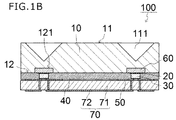
図1Aは、本実施形態にかかる発光モジュール100の模式平面図である。図1Bは、本実施形態にかかる発光モジュール100を示す一部拡大模式断面図である。図1Cは、実施形態にかかる導光板10の第1主面11の光学機能部111と、第2主面12の位置決め部121の一例を示す一部拡大模式平面図と一部拡大模式断面図である。
(Light emitting module)
The configuration of the light emitting module of this embodiment is shown in FIGS. 1A and 1B.
FIG. 1A is a schematic plan view of the
発光モジュール100は、導光板10と、複数の導光板10に接合された複数の発光素子30とを備える。複数の発光素子30は導光板10の第2主面12上にマトリクス状に配置されている。発光モジュール100の導光板10は、発光面となる第1主面11と、第1主面11と反対側の第2主面12と、を備える。第2主面12には、接合部材20によって発光素子30が接合されている。図1Bに示す例では、導光板10は第2主面12に位置決め部121として凹部を備えており、さらに凹部の内部には波長変換部材60を備えている。
The
尚、位置決め部(凹部)121及び波長変換部材60は省略してもよい。例えば、図1Dに示す発光モジュール100Aは、導光板10Aの第2主面12Aは凹部を備えておらず平坦な面である。そのため波長変換部材60の側面は被覆部材40Aで被覆されている。また、図1Eに示す発光モジュール100Bは、導光板10Aは図1Dに示す例と同様に凹部を備えておらず、第2主面12Aは平坦であり、さらに、波長変換部材を備えていない。そのため、発光素子30と導光板10Aの間には接合部材20のみが存在する。
The positioning portion (recess) 121 and the
このような発光モジュールは、以下の工程を備える製造方法により得ることができる。
発光モジュールの製造方法は、
(1)半導体積層体と電極とを備える発光素子を準備する工程
(2)発光面となる第1主面と、第1主面と反対側の第2主面と、を備える導光板を準備する工程
(3)導光板の第2主面上に、複数の接合部材を配置する工程
(4)複数の接合部材の上面の高さを揃える工程
(5)各接合部材上に、電極を上にして発光素子を載置する工程
(6)電極を含む発光素子を被覆する被覆部材を配置する工程
(7)電極が露出するまで被覆部材を除去する工程
(8)複数の発光素子を電気的に接続する導電部材を形成する工程
を備える。
Such a light emitting module can be obtained by a manufacturing method including the following steps.
The manufacturing method of the light emitting module is
(1) Step of preparing a light emitting element including a semiconductor laminate and an electrode (2) Preparing a light guide plate including a first main surface to be a light emitting surface and a second main surface opposite to the first main surface. (3) A process of arranging a plurality of joining members on the second main surface of the light guide plate (4) A step of aligning the heights of the upper surfaces of the plurality of joining members (5) An electrode is placed on each joining member. (6) A step of arranging a covering member for covering the light emitting element including the electrode (7) A step of removing the covering member until the electrode is exposed (8) Electrically connecting a plurality of light emitting elements A step of forming a conductive member to be connected to is provided.
本開示に係る発光モジュールは、導光板上に発光素子を接合しているため、薄型化が可能となる。また、導光板上に発光素子を搭載し、接着するため、基板上に発光素子を実装したものと導光板とを組み合わせる場合と比べ、発光素子と導光板と位置ずれが発生しづらい。これにより、良好な光学特性を備える発光モジュールとすることができる。さらに、接合部材の高さを揃えることで、発光素子の高さバラつきを低減することができる。そのため、導光板に反りがある場合等においても、被覆部材の除去により電極を露出させる工程において確実に電極を露出させることができる。 Since the light emitting module according to the present disclosure has a light emitting element bonded to the light guide plate, it can be made thinner. Further, since the light emitting element is mounted on the light guide plate and adhered to each other, the position shift between the light emitting element and the light guide plate is less likely to occur as compared with the case where the light emitting element is mounted on the substrate and the light guide plate is combined. This makes it possible to obtain a light emitting module having good optical characteristics. Further, by making the heights of the joining members uniform, it is possible to reduce the height variation of the light emitting element. Therefore, even when the light guide plate is warped, the electrodes can be reliably exposed in the step of exposing the electrodes by removing the covering member.
本実施形態にかかる発光モジュール100の製造方法の各工程について、以下に詳述する。図2A〜図2Kに本実施形態の発光モジュールの製造方法の一例を示す。
Each step of the method for manufacturing the
(1)半導体積層体と電極とを備える発光素子を準備する工程
発光素子30は、発光モジュール100の光源である。発光素子30は、複数が1つの導光板10に接合される。発光モジュール100の大きさや目的とする光学特性に応じて、必要な発光素子を準備する。発光素子は、半導体成長等の工程を経るなど、製造工程の一部又は全部を経ることで準備することができ、あるいは、購入等により準備してもよい。
(1) Step of Preparing a Light Emitting Element with a Semiconductor Laminated Body and Electrodes The
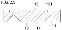
(2)発光面となる第1主面と、第1主面と反対側の第2主面と、を備える導光板を準備する工程
図2Aに示すように、導光板10を準備する。導光板10は、発光素子30からの光を面状に広げる部材であり、光取り出し面である第1主面11と、その反対側に位置する第2主面12とを備えた略板状の部材である。
(2) Step of preparing a light guide plate including a first main surface serving as a light emitting surface and a second main surface opposite to the first main surface As shown in FIG. 2A, the
導光板10は、図2Aに示すように、第1主面11に円錐状に凹んだ光学機能部111を備えてもよい。さらに、導光板10は第2主面12に開口が略四角形の凹部(位置決め部)121を備えてもよい。
As shown in FIG. 2A, the
拡散部材や波長変換部材を備える場合は、図2Bに示すように、導光板10の第2主面12の凹部121内に、拡散部材60を配置する工程を備える。拡散部材60は、発光素子からの光を拡散させる部材である。拡散部材60は、例えば、光拡散物質と樹脂材料との混合材料である。拡散部材60は、さらに、発光素子からの光を吸収して異なる波長の光に変換する蛍光体を含む波長変換部材であってもよい。
When a diffusion member or a wavelength conversion member is provided, as shown in FIG. 2B, a step of arranging the
拡散部材60の配置方法としては、例えば、液状の拡散部材の材料をポッティング、印刷、スプレー等で第2主面12上、又は第2主面12に設けた凹部121内に配置する方法が挙げられる。この場合、凹部121内に入らなかった余分の拡散部材の材料がある場合は、凹部121外の拡散部材の材料を第2主面12上から除去してもよい。図2Bに示す例では、第2主面12上に配置した拡散部材の材料を、スキージ80を用いて凹部121内に配置している。そして、液状の拡散部材の材料を硬化させることで、図2Bに示すように、位置決め部121内のそれぞれに、拡散部材60形成する。
As a method of arranging the
また、あらかじめ板状等に成形された拡散部材60の成形品を準備し、位置決め部121に載置する方法を用いてもよい。拡散部材60の成形品の形成方法は、例えば、大面積の板状又はシート状の拡散部材を、切断、パンチング等によって個片化する方法が挙げられる。あるいは、金型等を用いて射出成形、トランスファモールド法、圧縮成形などの方法によって小片の拡散部材60の成形品を形成することができる。拡散部材60の成形品は、接着剤等を用いて位置決め部(凹部)121内、又は、導光板10の第2主面12上に接着することができる。
Alternatively, a method may be used in which a molded product of the
(3)導光板の前記第2主面上に、複数の接合部材を配置する工程
次に、図2Cに示すように、それぞれの拡散部材60の上に液状の接合部材20をそれぞれ塗布する。接合部材20は、ポッティング、転写、印刷等の方法で塗布することができる。図2Cでは、ディスペンスノズル81を用いてポッティングすることで接合部材20を塗布する場合を例示しており、塗布された接合部材20の上面21は、凸曲面状となっている。
(3) Step of arranging a plurality of joining members on the second main surface of the light guide plate Next, as shown in FIG. 2C, a
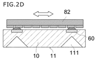
(4)複数の接合部材の上面の高さを揃える工程
次に、図2Dに示すように、複数の接合部材の上面の高さを揃える。ここでは、砥石等の研削部材82を用いて接合部材を研削している。これにより、図2Eに示すように、接合部材20の上面21の高さを揃えている。尚、ここでの「高さ」とは、接合部材20の厚みを指すものではなく、上面21の位置を指す。また、接合部材20を押圧することで、その上面の高さを揃えてもよい。
(4) Step of Aligning the Heights of the Upper Surfaces of a plurality of Joining Members Next, as shown in FIG. 2D, the heights of the upper surfaces of the plurality of joining members are aligned. Here, the joining member is ground using a grinding
(5)各接合部材上に、電極を上にして発光素子を載置する工程
次に、図2Fに示すように、それぞれの接合部材20の上面21に発光素子30を載置する。この時、電極32(電極形成面312)を上に発光素子30を載置する。つまり、主発光面311を接合部材20の上面21と対向するように載置する。その後、接合部材を硬化させ、発光素子30と導光板10とを接合する。
(5) Step of placing the light emitting element on each joining member with the electrode facing up Next, as shown in FIG. 2F, the
複数の発光素子30は、導光板10の平面視において、二次元に配列される。好ましくは、複数の発光素子30は、図1Aに示すように、直交する二方向、つまり、x方向(横方向)およびy方向(縦方向)に沿って二次元的に配列される。複数の光学機能部111に対応するように配置される複数の発光素子30のx方向の配列ピッチとy方向の配列ピッチは、同じであってもよいし、異なっていてもよい。また、配列の二方向は、直交していなくてもよい。また、x方向またはy方向の配列ピッチは等間隔に限られず、不等間隔であってもよい。例えば、導光板10の中央から周辺に向かって間隔が広くなるように発光素子30が配列されていてもよい。なお、発光素子30間のピッチとは、発光素子30の光軸間の距離である。発光素子30間のピッチは、例えば、0.05mm〜20mm程度とすることができ、1mm〜10mm程度が好ましい。
The plurality of
(6)電極を含む発光素子を被覆する被覆部材を配置する工程
次に、図2Gに示すように、導光板10の第2主面12と複数の発光素子30とを被覆する被覆部材40を形成する。被覆部材40は、例えばトランスファモールド、ポッティング、印刷、スプレー等の方法で形成することができる。この時、発光素子30の電極32の上面を完全に被覆するように被覆部材40を厚く形成する。
(6) Step of Arranging the Covering Member that Covers the Light Emitting Element Containing the Electrode Next, as shown in FIG. 2G, the covering
(7)電極が露出するまで被覆部材を除去する工程
次に、図2Hに示すように、被覆部材40の一部を研削し、発光素子30の電極32を露出させる。研削の方法としては、砥石等の研削部材を用いて被覆部材40を面状に研削している。接合部材20を研削して高さを揃えているために、複数の発光素子30のそれぞれの電極32が露出される。
(7) Step of Removing Covering Member Until The Electrode Is Exposed Next, as shown in FIG. 2H, a part of the covering
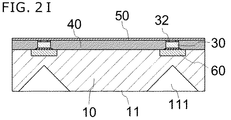
(8)複数の発光素子を電気的に接続する導電部材を形成する工程
次に、図2Iに示すように、発光素子30の電極32と被覆部材40上の略全面に、導電部材50となる金属膜を形成する。金属膜としては、例えば、導光板10側からCu/Ni/Auの順に積層させた積層構造とすることができる。金属膜の形成方法としては、スパッタ、メッキ等が挙げられ、スパッタで形成することが好ましい。
(8) Step of Forming a Conductive Member for Electrically Connecting a plurality of Light Emitting Elements Next, as shown in FIG. 2I, the
次に、図2Jに示すように、金属膜にレーザ光を照射し、照射した部分の金属膜を除去するレーザアブレーションによってパターニングし、導電部材50を形成する。
Next, as shown in FIG. 2J, the metal film is irradiated with laser light, and patterning is performed by laser ablation to remove the metal film of the irradiated portion to form the
次に、図2Kに示すように、この導電部材50と別途準備した配線基板70の配線層72とを接着シートを間に介して圧着して接合する。この時、配線層72の一部(例えばビア)内に充填された導電性材料を加圧と加熱によって一部溶解させることで、導電部材50と配線層72とを電気的に接続する。
このようにして、本実施形態の発光モジュール100を得ることができる。
Next, as shown in FIG. 2K, the
In this way, the
複数の発光素子30は、それぞれが独立で駆動するように配線されてもよい。また、導光板10を複数の範囲に分割し、1つの範囲内に実装された複数の発光素子30を1つのグループとし、1つのグループ内の複数の発光素子30同士を直列又は並列に電気的に接続することで同じ回路に接続し、このような発光素子グループを複数備えるようにしてもよい。このようなグループ分けを行うことで、ローカルディミング可能な発光モジュールとすることができる。
The plurality of
本実施形態の発光モジュール100は、1つが1つの液晶ディスプレイ装置のバックライトとして用いられてもよい。また、複数の発光モジュール100が並べられて1つの液晶ディスプレイ装置のバックライトとして用いられてもよい。小さい発光モジュール100を複数作り、それぞれ検査等を行うことで、大きく実装される発光素子30の数が多い発光モジュール100を作成する場合と比べて、歩留まりを向上させることができる。
One of the
1つの発光モジュール100は1つの配線基板70に接合されてもよい。また、複数の発光モジュール100が、1つの配線基板70に接合されてもよい。これにより、外部との電気的な接続端子(例えばコネクタ)を集約できる(つまり、発光モジュール1つごとに用意する必要がない)ため、液晶ディスプレイ装置の構造を簡易にすることができる。
One
また、この複数の発光モジュール100が接合された1つの配線基板70を複数並べて一つの液晶ディスプレイ装置のバックライトとしてもよい。この時、例えば、複数の配線基板70をフレーム等に載置し、それぞれコネクタ等を用いて外部の電源と接続することができる。
Further, a plurality of one
発光モジュールを構成する各部材について、以下に詳述する。 Each member constituting the light emitting module will be described in detail below.
(発光素子)
発光素子30は、公知の半導体発光素子を利用することができる。本実施形態においては、発光素子30として発光ダイオードを例示する。発光素子は、主に発光を取り出す主発光面311と、主発光面311と反対側の電極形成面312に一対の電極32を有する。一対の電極32は後述する配線基板70と対向して配置され、任意に導電部材50等を介して、適宜配線基板70の配線層72と電気的に接続される。
(Light emitting element)
As the
発光素子30は、例えば、サファイア等の透光性基板と、透光性基板の上に積層された半導体層とを備えた半導体積層体を備える。半導体積層体31は、発光層と、発光層を挟むn型半導体層およびp型半導体層とを含み、n型半導体層およびp型半導体層にn側電極およびp側電極がそれぞれ電気的に接続される。発光素子30は、例えば透光性基板を備える主発光面311が導光板と対向して配置され、主発光面311と反対側の電極形成面312に一対の電極32を有する。
The
発光素子30、任意の波長の光を出射する素子を選択することができる。例えば、青色、緑色の光を出射する素子としては、窒化物系半導体(InxAlyGa1−x−yN、0≦X、0≦Y、X+Y≦1)またはGaPを用いた発光素子を用いることができる。また、赤色の光を出射する素子としては、GaAlAs、AlInGaPなどの半導体を含む発光素子を用いることができる。さらに、これら以外の材料からなる半導体発光素子を用いることもできる。半導体層の材料およびその混晶度によって発光波長を種々選択することができる。用いる発光素子の組成、発光色、大きさ、個数などは、目的に応じて適宜選択すればよい。発光モジュール100が波長変換部材を備える場合、発光素子30は、波長変換部材を効率良く励起できる短波長の光を出射することが可能な窒化物半導体(InxAlyGa1−x−yN、0≦X、0≦Y、X+Y≦1)を備えることが好ましい。
The
発光素子30の大きさは、例えば、平面視において縦および横の寸法は1000μm以下が好ましく、より好ましくは縦および横の寸法が500μm以下であり、さらに好ましくは、縦および横の寸法が200μm以下である。このような発光素子を用いると、液晶ディスプレイ装置のローカルディミングを行った際に、高精細な映像を実現することができる。
The size of the
(導光板)
導光板10は、発光素子からの光が入射され、面状の発光を行う透光性の板状部材である。導光板10は、発光面となる第1主面11と、第1主面11と反対側の第2主面12と、を備える。
(Light guide plate)
The
導光板10の大きさは、例えば、一辺が1cm〜200cm程度とすることができ、3cm〜30cm程度が好ましい。厚みは0.1mm〜5mm程度とすることができ、0.5mm〜3mmが好ましい。尚、ここでの「厚み」とは、例えば、第1主面11や第2主面12に凹部や凸部等がある場合は、それらがないものと仮定した場合の厚みを指すものとする。
導光板1の平面形状は例えば、略矩形や略円形等とすることができる。
The size of the
The planar shape of the light guide plate 1 can be, for example, a substantially rectangular shape, a substantially circular shape, or the like.
導光板10の材料としては、アクリル、ポリカーボネート、環状ポリオレフィン、ポリエチレンテレフタレート、ポリエステル等の熱可塑性樹脂、エポキシ、シリコーン等の熱硬化性樹脂等の樹脂材料やガラスなどの光学的に透明な材料を用いることができる。特に、熱可塑性の樹脂材料は、射出成型によって効率よく製造することができるため、好ましい。なかでも、透明性が高く、安価なポリカーボネートが好ましい。導光板10に発光素子30を接合した後に配線基板を貼りつける本実施形態の発光装置の製造方法においては、半田リフローのような高温がかかる工程を省略できるため、ポリカーボネートのような熱可塑性であり耐熱性の低い材料であっても用いることができる。
As the material of the
導光板10は、例えば、射出成型やトランスファモールド、熱転写等で成形することができる。導光板10が光学機能部111や位置決め部121を備えている場合には、これらも一括して金型で形成することができる。これにより、光学機能部111と位置決め部121の成形位置ずれを低減することができる。
The
導光板10は単層で形成されていてもよく、複数の透光性の層が積層されて形成されていてもよい。複数の透光性の層が積層されている場合には、任意の層間に屈折率の異なる層、例えば空気の層等を設けてもよい。これにより、光をより拡散させやすくなり、輝度ムラを低減した発光モジュールとすることができる。このような構成は、例えば、任意の複数の透光性の層の間にスペーサを設けて離間させ、空気の層を設けることで実現することができる。
The
(光学機能部)
導光板10は、第1主面11側に光学機能部111を備えていてもよい。光学機能部111は、例えば、光を導光板10の面内で広げる機能を有することができる。例えば、導光板10の材料と屈折率の異なる材料が設けられている。具体的には、光学機能部111は、第1主面11側に設けられた円錐や四角錐、六角錐等の多角錐形等の凹みであって、導光板10と屈折率の異なる材料(例えば空気)と凹みの傾斜面との界面で照射された光を発光素子30の側方方向に反射するものを用いることができる。また、光学機能部は円錐台や、四角錐台等の多角錐台とすることができる。図1Fに示す発光モジュール100Cでは、導光板10Bは、円錐台の光学機能部111Aを備えており、このような光学機能部111Aは断面視において台形となる。錐台形の光学機能部111Aの場合、また例えば、傾斜面を有する凹部に光反射性の材料(例えば金属等の反射膜や白色の樹脂)等を設けたものであってもよい。光学機能部111の傾斜面は、断面視において直線でもよく、曲線でもよい。
光学機能部111は、後述するように、それぞれの発光素子30に対応する、つまり、第2主面12側に配置された発光素子30と反対側の位置に設けられることが好ましい。特に、発光素子30の光軸と、光学機能部111の光軸とが略一致することが好ましい。
(Optical function unit)
The
As will be described later, the
光学機能部111の大きさは、適宜設定することができる。図1Bに示す光学機能部111は、第1主面11において円形の開口部を備える円錐状の凹部であり、開口の直径は波長変換部材60よりも大きい例を示している。
The size of the
(位置決め部(凹部))
導光板10は、第2主面12側に、位置決め部121を備えていてもよい。位置決め部121は、発光素子30を配置する位置の目標とする部分であり、例えば、図1B等に示すような凹部や、凸部、溝等とすることができる。
位置決め部121の平面視における大きさは、例えば、0.05mm〜10mmとすることができ、0.1mm〜1mmが好ましい。深さは0.05mm〜4mmとすることができ、0.1mm〜1mmが好ましい。光学機能部111と位置決め部121の間の距離は、光学機能部111と位置決め部121が離間している範囲で適宜設定できる。
(Positioning part (recess))
The
The size of the
位置決め部121の平面視形状は、例えば、略矩形、略円形とすることができ、位置決め部の配列ピッチ等によって選択可能である。位置決め部の配列ピッチ(最も近接した2つの位置決め部の間の距離)が略均等である場合には、略円形または略正方形が好ましい。なかでも、略円形とすることで、発光素子30からの光を良好に広げることができる。
The plan-view shape of the
(拡散部材)
導光板の第2主面側に配置される拡散部材は、発光素子30からの光を拡散させる光拡散物質を含有する部材である。また、拡散部材は、発光素子30からの光の波長を異なる波長の光に変換する蛍光体を含有する波長変換部材であってもよい。さらに、蛍光体を含有する蛍光体含有層と、蛍光体を含有しない蛍光体非含有層とを積層させた拡散部材としてもよい。あるいは、蛍光体を含有する蛍光体含有層と、波長を変換しない光拡散物質を含有する拡散層とを積層させた拡散部材としてもよい。
(Diffusion member)
The diffusing member arranged on the second main surface side of the light guide plate is a member containing a light diffusing substance that diffuses the light from the
拡散部材や波長変換部材は、発光素子30と導光板10との間に設けられ、導光板10の第2主面12側に配置されている。拡散部や波長変換部材は、それに照射された発光素子30からの光を拡散し、均等化する。拡散部材(波長変換部材)は、図1Bに示すように、導光板10の位置決め部(凹部)121内に配置することができる。あるいは、図1Dに示すように、平坦な導光板10の第2主面12上に配置され、第2主面12突出するように設けられていてもよい。
The diffusion member and the wavelength conversion member are provided between the light emitting
拡散部材60の大きさや形状は、例えば、位置決め部として凹部を備える場合は、その凹部と同等程度とすることができる。また、拡散部材60の高さは、位置決め部として凹部を備える場合は、その深さと同程度とすることが好ましい。
The size and shape of the
なお、導光板10には、光学機能部111以外の部分に光拡散、反射等をさせる加工を有していてもよい。例えば、光学機能部111から離間した部分に微細な凹凸を設ける、または粗面としてもよい。これにより、さらに光を拡散させ、輝度ムラを低減するようにすることができる。
The
拡散部材60は、導光板10の材料よりも高い屈折率を有する材料が好ましい。例えば、母材の材料として、エポキシ樹脂、シリコーン樹脂、これらを混合した樹脂、または、ガラスなどの透光性材料を用いることができる。拡散部材60の耐光性および成形容易性の観点からは、拡散部材60の母材としてシリコーン樹脂を選択すると有益である。
The
光拡散物質としては、例えばSiO2、TiO2、Al2O3、ZnO等の微粒子が挙げられる。 Examples of the light diffusing substance include fine particles such as SiO 2 , TiO 2 , Al 2 O 3, and ZnO.
拡散部材60は、波長変換物質として粒子状の蛍光体を含むことができる。蛍光体としては、例えば、YAG系蛍光体、βサイアロン蛍光体またはKSF系蛍光体等のフッ化物系蛍光体などが挙げられる。1つの拡散部材60に、1種類又は複数種類の蛍光体を含むことができる。複数種類の蛍光体は、混合させて用いてもよく、あるいは積層させて用いてもよい。例えば、青色系の光を出射する発光素子30を用い、蛍光体として緑色系の発光をするβサイアロン蛍光体と赤色系の発光をするKSF系蛍光体等のフッ化物系蛍光体とを含むことができる。このような2種類の蛍光体を用いることで、発光モジュールの色再現範囲を広げることができる。また、蛍光体は量子ドットであってもよい。
The
拡散部材60が蛍光体を含む場合、その内部において蛍光体はどのように配置されていてもよい。例えば、略均一に分布していてもよく、一部に偏在してもよい。
When the diffusing
(接合部材)
接合部材20は、発光素子30から出射される光を導光板10に伝播させる役割を有する。接合部材20は、発光素子30と導光板10とを、直接又は間接的に接合する部材である。間接的に接合する、とは、導光板10に配置された拡散部材又は波長変換部材60と、発光素子30とが接合部材20によって接合されることを指す。
(Joining member)
The joining
接合部材20は、透光性であり、発光素子30から出射される光の60%以上を透過し、好ましくは90%以上を透過する。そのため、接合部材20は、拡散部材等を含むことは可能であり、拡散部材等を含まない透光性の樹脂材料のみで構成されてもよい。
The joining
接合部材20は、発光素子30の側面(主発光面311と電極形成面312をつなぐ面)を被覆していてもよい。これにより、発光素子30の側面方向に出射された光を接合部材20内に効率的に取り出し、発光モジュール100の発光効率を高めることができる。
The joining
接合部材20の材料としては、エポキシ樹脂、シリコーン樹脂等の透光性の熱硬化性の樹脂材料等を用いることができる。
As the material of the joining
(被覆部材)
被覆部材40は、複数の発光素子30の側面と導光板10の第2主面12と接合部材20の側面とを被覆している。これにより、発光素子30と導光板10を補強することができる。また、被覆部材40は、光反射性部材であることが好ましい。被覆部材40を光反射性部材とすることで、発光素子30からの発光を導光板10に効率よく取り入れることができる。なお、図1Dに示すように、拡散部材(波長変換部材)60が導光板10の第2主面上に設けられ、その拡散部材60の側面等の面が導光板10から露出している場合には、その露出した部分も被覆部材40で被覆することが好ましい。
(Coating member)
The covering
光反射性部材の被覆部材40は、発光素子30から出射される光に対して60%以上の反射率を有し、好ましくは90%以上の反射率を有する。光反射性部材の被覆部材40の材料は、白色の顔料等を含有させた樹脂材料であることが好ましい。特に、酸化チタンを含有させたシリコーン樹脂が好ましい。これにより、導光板10の一面を被覆するために比較的大量に用いられる材料として酸化チタンのような安価な原材料を多く用いることで、発光モジュール100を安価にすることができる。
The coating
(導電部材)
発光モジュール100には、複数の発光素子30の電極32と電気的に接続される導電部材50が設けられていてもよい。導電部材50は、被覆部材40の下面と電極32の下面とを被覆するように配置される。導電部材50を設けることにより、例えば複数の発光素子30同士を電気的に接続することができ、液晶ディスプレイ装置ローカルディミング等に必要な回路を容易に形成することができる。
(Conductive member)
The
(配線基板)
発光モジュール100は、図2Kに示すように、配線基板70を有していてもよい。配線基板70は、絶縁性の基材71と、複数の発光素子30と電気的に接続される配線層72等を備える基板である。配線基板70を備えることで、ローカルディミング等に必要な複雑な配線を容易に形成することができる。この配線基板70は、発光素子30を導光板10に実装し、任意に被覆部材40及び導電部材50を形成した後に、別途準備した配線基板70の配線層72と、導電部材50とを、接合することで形成することができる。また、発光素子30と接続する導電部材50を設ける際、導電部材50を発光素子30の電極32の平面形状よりも大きい形状とすることで、この配線基板70と発光素子30との電気的な接合を容易に行うことができる。
(Wiring board)
The
配線基板70は、例えば、絶縁性の基材71に設けられた複数のビアホール内に充填された導電性部材と、基材71の両面側において導電性部材と電気的に接続された配線層72と、を備える。
The
配線基板70の基材71の材料としては、どのようなものであってもよい。例えば、セラミックスおよび樹脂を用いることができる。低コストおよび成形容易性の点から、樹脂を基材71の材料として選択してもよい。樹脂としては、フェノール樹脂、エポキシ樹脂、ポリイミド樹脂、BTレジン、ポリフタルアミド(PPA)、ポリエチレンテレフタレート(PET)、不飽和ポリエステル、ガラスエポキシ等の複合材料等を挙げることができる。また、リジッド基板であってもよく、フレキシブル基板であってもよい。
Any material may be used as the material of the
配線層72は、例えば、基材71上に設けられた導電箔(導体層)であり、複数の発光素子30と電気的に接続される。配線層72の材料は、高い熱伝導性を有していることが好ましい。このような材料として、例えば銅などの導電材料が挙げられる。また、配線層72は、メッキや導電性ペーストの塗布、印刷などで形成することができ、配線層72の厚みは、例えば、5〜50μm程度である。
The
配線基板70は、どのような方法で導光板10等と接合されていてもよい。例えば、シート状の接着シートを、導光板10の反対側に設けられた被覆部材40の表面と、配線基板70の表面との間に配置し、圧着することで、接合することができる。また、配線基板70の配線層72と発光素子30との電気的接続はどのような方法で行われてもよい。例えば、ビアホール内に埋め込んだ金属である導電性部材を加圧と加熱により溶かして導電部材50と接合することができる。
The
なお、配線基板70は、積層構造を有していてもよい。例えば、配線基板70として、表面に絶縁層が設けられた金属板を用いてもよい。また、配線基板70は複数のTFT(Thin−Film Transistor)を有するTFT基板であってもよい。
The
本開示に係る発光モジュールは、例えば、液晶ディスプレイ装置のバックライトとして利用することができる。 The light emitting module according to the present disclosure can be used, for example, as a backlight of a liquid crystal display device.
100、100A、100B、100C…発光モジュール
10、10A、10B…導光板
11…第1主面(光取り出し面)
111、111A…光学機能部
12、12A…第2主面
121…位置決め部(凹部)
20…接合部材
21…接合部材の上面
30…発光素子
31…半導体積層体
311…主発光面
312…電極形成面
32…電極
40、40A…被覆部材
50…導電部材
60…拡散部材(波長変換部材)
70…配線基板
71…基材
72…配線層
80…スキージ
81…ディスペンスノズル
82…研削部材
100, 100A, 100B, 100C ...
111, 111A ...
20 ... Joining
70 ... Wiring
Claims (7)
発光面となる第1主面と、前記第1主面と反対側の第2主面と、を備える導光板を準備する工程と、
前記導光板の前記第2主面上に、複数の接合部材を配置する工程と、
前記複数の接合部材の上面の高さを揃える工程と、
上面の高さを揃えた前記各接合部材上に、前記電極を上にして発光素子を載置する工程と、
前記電極を含む発光素子を被覆する被覆部材を配置する工程と、
前記電極が露出するまで前記被覆部材を除去する工程と、
前記複数の発光素子を電気的に接続する導電部材を形成する工程と、
を備える発光モジュールの製造方法。 The process of preparing a light emitting element including a semiconductor laminate and electrodes,
A step of preparing a light guide plate including a first main surface serving as a light emitting surface and a second main surface opposite to the first main surface.
A step of arranging a plurality of joining members on the second main surface of the light guide plate, and
The process of aligning the heights of the upper surfaces of the plurality of joining members and
A step of placing the light emitting element with the electrode facing up on each of the joining members having the same height on the upper surface, and
The step of arranging the covering member for covering the light emitting element including the electrode, and
The step of removing the covering member until the electrode is exposed, and
A step of forming a conductive member that electrically connects the plurality of light emitting elements, and
A method of manufacturing a light emitting module comprising.
前記接合部材は、前記拡散部材上に配置される、請求項1〜請求項3のいずれか1項に記載の発光モジュールの製造方法。 The light guide plate has a recess on the second main surface side, and has a step of arranging a diffusion member in the recess.
The method for manufacturing a light emitting module according to any one of claims 1 to 3, wherein the joining member is arranged on the diffusion member.
Priority Applications (1)
| Application Number | Priority Date | Filing Date | Title |
|---|---|---|---|
| JP2018118397A JP6963183B2 (en) | 2018-06-22 | 2018-06-22 | Manufacturing method of light emitting module |
Applications Claiming Priority (1)
| Application Number | Priority Date | Filing Date | Title |
|---|---|---|---|
| JP2018118397A JP6963183B2 (en) | 2018-06-22 | 2018-06-22 | Manufacturing method of light emitting module |
Publications (3)
| Publication Number | Publication Date |
|---|---|
| JP2019220405A JP2019220405A (en) | 2019-12-26 |
| JP2019220405A5 JP2019220405A5 (en) | 2020-04-02 |
| JP6963183B2 true JP6963183B2 (en) | 2021-11-05 |
Family
ID=69096886
Family Applications (1)
| Application Number | Title | Priority Date | Filing Date |
|---|---|---|---|
| JP2018118397A Active JP6963183B2 (en) | 2018-06-22 | 2018-06-22 | Manufacturing method of light emitting module |
Country Status (1)
| Country | Link |
|---|---|
| JP (1) | JP6963183B2 (en) |
Families Citing this family (2)
| Publication number | Priority date | Publication date | Assignee | Title |
|---|---|---|---|---|
| JP7148810B2 (en) * | 2020-02-18 | 2022-10-06 | 日亜化学工業株式会社 | Light-emitting module manufacturing method and light-emitting module |
| JP7328568B2 (en) | 2021-06-30 | 2023-08-17 | 日亜化学工業株式会社 | Light source, light source device, and light source manufacturing method |
Family Cites Families (5)
| Publication number | Priority date | Publication date | Assignee | Title |
|---|---|---|---|---|
| JP5052860B2 (en) * | 2005-12-15 | 2012-10-17 | 三菱電機株式会社 | Planar light source device and display device using the same |
| CN102472916B (en) * | 2009-08-13 | 2015-02-18 | 株式会社大华 | Gel member for optical use, method for assembling optical device using same, and optical device |
| DE102010018260A1 (en) * | 2010-01-29 | 2011-08-04 | OSRAM Opto Semiconductors GmbH, 93055 | lighting device |
| EP2378322B1 (en) * | 2010-04-10 | 2014-01-08 | LG Innotek Co., Ltd. | Light source device |
| JP6413631B2 (en) * | 2014-10-28 | 2018-10-31 | 日亜化学工業株式会社 | LIGHT EMITTING DEVICE AND LIGHT EMITTING DEVICE MANUFACTURING METHOD |
-
2018
- 2018-06-22 JP JP2018118397A patent/JP6963183B2/en active Active
Also Published As
| Publication number | Publication date |
|---|---|
| JP2019220405A (en) | 2019-12-26 |
Similar Documents
| Publication | Publication Date | Title |
|---|---|---|
| JP7161117B2 (en) | light emitting module | |
| JP6790899B2 (en) | Light emitting module manufacturing method and light emitting module | |
| TWI744756B (en) | Light emitting module | |
| US11073654B2 (en) | Light emitting module with recesses in light guide plate | |
| JP6912730B2 (en) | Manufacturing method of light emitting module | |
| JP7108203B2 (en) | Method for manufacturing light-emitting module | |
| JP7116331B2 (en) | Light-emitting module manufacturing method and light-emitting module | |
| JP7007591B2 (en) | Luminous module | |
| KR102111200B1 (en) | Manufacturing method for light emitting module and light emitting module | |
| JP6963183B2 (en) | Manufacturing method of light emitting module | |
| US11194089B2 (en) | Method for manufacturing light emitting module | |
| JP7208470B2 (en) | Light-emitting module manufacturing method and light-emitting module | |
| JP7111993B2 (en) | Method for manufacturing light-emitting module | |
| JP6848942B2 (en) | Manufacturing method of light emitting module | |
| JP7068594B2 (en) | Light emitting module manufacturing method and light emitting module | |
| JP2020027774A (en) | Light emitting module and method of manufacturing the same | |
| JP2021125371A (en) | Manufacturing method of light emitting module |
Legal Events
| Date | Code | Title | Description |
|---|---|---|---|
| A521 | Written amendment |
Free format text: JAPANESE INTERMEDIATE CODE: A523 Effective date: 20200215 |
|
| A621 | Written request for application examination |
Free format text: JAPANESE INTERMEDIATE CODE: A621 Effective date: 20200215 |
|
| A977 | Report on retrieval |
Free format text: JAPANESE INTERMEDIATE CODE: A971007 Effective date: 20201203 |
|
| A131 | Notification of reasons for refusal |
Free format text: JAPANESE INTERMEDIATE CODE: A131 Effective date: 20210112 |
|
| A521 | Written amendment |
Free format text: JAPANESE INTERMEDIATE CODE: A523 Effective date: 20210311 |
|
| A131 | Notification of reasons for refusal |
Free format text: JAPANESE INTERMEDIATE CODE: A131 Effective date: 20210518 |
|
| A521 | Written amendment |
Free format text: JAPANESE INTERMEDIATE CODE: A523 Effective date: 20210713 |
|
| TRDD | Decision of grant or rejection written | ||
| A01 | Written decision to grant a patent or to grant a registration (utility model) |
Free format text: JAPANESE INTERMEDIATE CODE: A01 Effective date: 20210914 |
|
| A61 | First payment of annual fees (during grant procedure) |
Free format text: JAPANESE INTERMEDIATE CODE: A61 Effective date: 20210927 |
|
| R150 | Certificate of patent or registration of utility model |
Ref document number: 6963183 Country of ref document: JP Free format text: JAPANESE INTERMEDIATE CODE: R150 |