JP7148810B2 - Light-emitting module manufacturing method and light-emitting module - Google Patents

Light-emitting module manufacturing method and light-emitting module Download PDF

Info

Publication number
JP7148810B2
JP7148810B2 JP2020025027A JP2020025027A JP7148810B2 JP 7148810 B2 JP7148810 B2 JP 7148810B2 JP 2020025027 A JP2020025027 A JP 2020025027A JP 2020025027 A JP2020025027 A JP 2020025027A JP 7148810 B2 JP7148810 B2 JP 7148810B2
Authority
JP
Japan
Prior art keywords
light
wavelength conversion
guide plate
emitting element
light emitting
Prior art date
Legal status (The legal status is an assumption and is not a legal conclusion. Google has not performed a legal analysis and makes no representation as to the accuracy of the status listed.)
Active
Application number
JP2020025027A
Other languages
Japanese (ja)
Other versions
JP2021131932A (en
Inventor
真一 大黒
Current Assignee (The listed assignees may be inaccurate. Google has not performed a legal analysis and makes no representation or warranty as to the accuracy of the list.)
Nichia Corp
Original Assignee
Nichia Corp
Priority date (The priority date is an assumption and is not a legal conclusion. Google has not performed a legal analysis and makes no representation as to the accuracy of the date listed.)
Filing date
Publication date
Application filed by Nichia Corp filed Critical Nichia Corp
Priority to JP2020025027A priority Critical patent/JP7148810B2/en
Publication of JP2021131932A publication Critical patent/JP2021131932A/en
Application granted granted Critical
Publication of JP7148810B2 publication Critical patent/JP7148810B2/en
Active legal-status Critical Current
Anticipated expiration legal-status Critical

Links

Images

Description

本開示は、発光モジュールの製造方法及び発光モジュールに関する。 TECHNICAL FIELD The present disclosure relates to a method for manufacturing a light emitting module and a light emitting module.

発光ダイオード等の発光素子と、導光板とを備える発光モジュールは、液晶ディスプレイのバックライトの光源及びディスプレイ等として広く利用されている(例えば、特許文献1、2等)。 A light-emitting module including a light-emitting element such as a light-emitting diode and a light guide plate is widely used as a backlight source for a liquid crystal display, a display, and the like (for example, Patent Documents 1 and 2).

特開2010-164976号公報JP 2010-164976 A 特表2015-525001号公報Japanese Patent Publication No. 2015-525001

本開示は、色ずれを低減した発光モジュールの製造方法及び発光モジュールを提供することを目的とする。 An object of the present disclosure is to provide a light-emitting module manufacturing method and a light-emitting module that reduce color shift.

本開示は以下の構成を含む。
(1)発光面となる第1主面と、前記第1主面の反対側であって、複数の凹部を備える第2主面を有する導光板を準備する工程と、
平面視において、前記凹部の面積よりも小さい面積の波長変換部材を準備する工程と、
第1面と該第1面の反対側の第2面とを備える半導体積層体及び前記第2面に配置される電極を備える発光素子と、前記発光素子の側面を被覆し、前記電極を露出する被覆部材とを備える光源を準備する工程と、
前記凹部内に前記波長変換部材を配置する工程と、
前記波長変換部材上に、前記発光素子における前記半導体積層体の前記第1面側を対向させて前記光源を固定する工程と、
前記光源と前記導光板の前記第2主面とを光反射部材で封止する工程と、
を含む発光モジュールの製造方法。
(2)発光面となる第1主面と、前記第1主面の反対側であって、複数の凹部を備える第2主面を有する導光板と、
前記導光板の前記凹部内に配置された波長変換部材と、
該波長変換部材に接合された光源であって、発光素子と、該発光素子の側面を被覆する被覆部材と、を備える光源と、
前記導光板の前記第2主面と前記光源とを封止する光反射部材と、
前記被覆部材と前記光反射部材との間に配置され、前記光源の側面の一部を被覆する透光性接合部材とを備え、
平面視において、前記光源の外縁が前記波長変換部材の外側に配置されてなる発光モジュール。
The present disclosure includes the following configurations.
(1) preparing a light guide plate having a first main surface serving as a light emitting surface and a second main surface opposite to the first main surface and having a plurality of recesses;
preparing a wavelength conversion member having an area smaller than the area of the recess in plan view;
A light-emitting element comprising a semiconductor laminate having a first surface and a second surface opposite to the first surface and an electrode disposed on the second surface; and covering a side surface of the light-emitting element and exposing the electrode. providing a light source comprising a covering member for
disposing the wavelength conversion member in the recess;
a step of fixing the light source on the wavelength conversion member with the first surface side of the semiconductor laminate of the light emitting element facing each other;
sealing the light source and the second main surface of the light guide plate with a light reflecting member;
A method of manufacturing a light emitting module comprising:
(2) a light guide plate having a first principal surface serving as a light emitting surface and a second principal surface opposite to the first principal surface and having a plurality of recesses;
a wavelength conversion member disposed within the recess of the light guide plate;
a light source joined to the wavelength conversion member, the light source including a light emitting element and a covering member covering the side surface of the light emitting element;
a light reflecting member that seals the second main surface of the light guide plate and the light source;
a translucent joining member disposed between the covering member and the light reflecting member and covering a part of a side surface of the light source;
A light-emitting module in which an outer edge of the light source is arranged outside the wavelength conversion member in plan view.

本開示によれば、色ずれを低減した発光モジュールを簡便に製造することができる製造方法及び色ずれを低減した発光モジュールを提供することができる。 According to the present disclosure, it is possible to provide a manufacturing method capable of easily manufacturing a light-emitting module with reduced color shift and a light-emitting module with reduced color shift.

本発明の一実施形態の発光モジュールの製造方法を示す概略断面図である。It is a schematic sectional drawing which shows the manufacturing method of the light emitting module of one Embodiment of this invention. 本発明の一実施形態の発光モジュールの製造方法を示す概略断面図である。It is a schematic sectional drawing which shows the manufacturing method of the light emitting module of one Embodiment of this invention. 本発明の一実施形態の発光モジュールの製造方法を示す概略断面図である。It is a schematic sectional drawing which shows the manufacturing method of the light emitting module of one Embodiment of this invention. 本発明の一実施形態の発光モジュールの製造方法を示す概略断面図である。It is a schematic sectional drawing which shows the manufacturing method of the light emitting module of one Embodiment of this invention. 本発明の一実施形態の発光モジュールの製造方法を示す概略断面図である。It is a schematic sectional drawing which shows the manufacturing method of the light emitting module of one Embodiment of this invention. 本発明の一実施形態の発光モジュールの製造方法を示す概略断面図である。It is a schematic sectional drawing which shows the manufacturing method of the light emitting module of one Embodiment of this invention. 本発明の一実施形態の発光モジュールの製造方法を示す概略断面図である。It is a schematic sectional drawing which shows the manufacturing method of the light emitting module of one Embodiment of this invention. 本発明の一実施形態の発光モジュールの製造方法を示す概略断面図である。It is a schematic sectional drawing which shows the manufacturing method of the light emitting module of one Embodiment of this invention. 発光モジュールの光源の製造方法を示す概略断面図である。It is a schematic sectional drawing which shows the manufacturing method of the light source of a light emitting module. 発光モジュールの光源の製造方法を示す概略断面図である。It is a schematic sectional drawing which shows the manufacturing method of the light source of a light emitting module. 発光モジュールの光源の製造方法を示す概略断面図である。It is a schematic sectional drawing which shows the manufacturing method of the light source of a light emitting module. 発光モジュールの光源の製造方法を示す概略断面図である。It is a schematic sectional drawing which shows the manufacturing method of the light source of a light emitting module. 発光モジュールの光源の製造方法を示す概略断面図である。It is a schematic sectional drawing which shows the manufacturing method of the light source of a light emitting module. 本発明の一実施形態の発光モジュールの一部の概略断面図である。1 is a schematic cross-sectional view of part of a light emitting module according to an embodiment of the invention; FIG. 本発明の別の実施形態の発光モジュールの一部の概略断面図である。FIG. 4 is a schematic cross-sectional view of part of a light emitting module according to another embodiment of the invention; 本発明のさらに別の実施形態の発光モジュールの一部の概略断面図である。FIG. 5 is a schematic cross-sectional view of part of a light emitting module of yet another embodiment of the invention; 本発明の一実施形態の発光モジュールの概略平面図である。1 is a schematic plan view of a light emitting module according to one embodiment of the present invention; FIG. 本発明の発光モジュールを利用した液晶ディスプレイ装置を示す分解斜視図である。1 is an exploded perspective view showing a liquid crystal display device using a light emitting module of the present invention; FIG.

以下、本発明を図面に基づいて詳細に説明する。以下の説明では、必要に応じて特定の方向又は位置を示す用語(例えば、「上」、「下」及びそれらの用語を含む別の用語)を用いる場合、それらの用語の使用は図面を参照して発明の理解を容易にするためであって、それらの用語の意味によって本発明の技術的範囲が制限されるものではない。例えば、発光モジュールの発光面側に配置される各部材の面を第1主面、第1面又は上面、発光面の反対側の面を第2主面、第2面又は下面と称することがある。複数の図面に表れる同一符号の部分は同一もしくは同等の部分又は部材を示す。
また、以下に示す実施形態は、本発明の技術思想を具体化するための発光モジュールを例示するものであって、本発明を以下に限定するものではない。さらに、以下に記載されている構成部品の寸法、材質、形状、その相対的配置等は、特定的な記載がない限り、本発明の範囲をそれのみに限定する趣旨ではなく、例示することを意図したものである。一の実施の形態、実施例において説明する内容は、他の実施の形態、実施例にも適用可能である。図面が示す部材の大きさ、位置関係等は、説明を明確にするため、誇張していることがある。
The present invention will now be described in detail with reference to the drawings. When the following description uses terms indicating a specific direction or position where necessary (e.g., "upper", "lower" and other terms that include those terms), refer to the drawings for the use of those terms. The meaning of these terms is not intended to limit the technical scope of the present invention. For example, the surface of each member arranged on the light emitting surface side of the light emitting module may be referred to as the first principal surface, first surface or top surface, and the surface opposite to the light emitting surface may be referred to as the second principal surface, second surface or bottom surface. be. Parts with the same reference numbers that appear in multiple drawings indicate the same or equivalent parts or members.
Moreover, the embodiments shown below are examples of light-emitting modules for embodying the technical idea of the present invention, and the present invention is not limited to the following. Furthermore, unless there is a specific description, the dimensions, materials, shapes, relative arrangements, etc. of the components described below are not intended to limit the scope of the present invention, but are intended to be illustrative. It is intended. The contents described in one embodiment and example can also be applied to other embodiments and examples. The sizes, positional relationships, etc. of members shown in the drawings may be exaggerated for clarity of explanation.

〔発光モジュールの製造方法〕
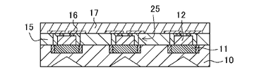
本開示の一実施形態の発光モジュールの製造方法で得られる発光モジュール20の一例は、図3Aに示すように、導光板10と、波長変換部材11と、光源25と、光反射部材15とを備える。
[Method for producing light-emitting module]
An example of a light-emitting module 20 obtained by a method for manufacturing a light-emitting module according to an embodiment of the present disclosure includes a light guide plate 10, a wavelength converting member 11, a light source 25, and a light reflecting member 15, as shown in FIG. 3A. Prepare.

導光板10は、図1Aに示すように、第1主面10Uと、第2主面10Bとを備える。第2主面10Bは、凹部10Rを備える。波長変換部材11は、凹部10R内に配置されている。光源25は、発光素子12と、発光素子12の側面を被覆する被覆部材13とを備える。光源25は、波長変換部材11に接合されている。光反射部材15は、導光板10の第2主面10Bと光源25とを封止している。 The light guide plate 10 includes a first main surface 10U and a second main surface 10B, as shown in FIG. 1A. The second main surface 10B has a recess 10R. The wavelength conversion member 11 is arranged inside the recess 10R. The light source 25 includes the light emitting element 12 and the covering member 13 covering the side surface of the light emitting element 12 . The light source 25 is joined to the wavelength conversion member 11 . The light reflecting member 15 seals the second main surface 10B of the light guide plate 10 and the light source 25 .

本開示の一実施形態の発光モジュールの製造方法は、主に以下の工程を含む。
発光面となる第1主面10Uと、第1主面10Uと反対側の第2主面10Bであって、複数の凹部10Rを備える第2主面10Bと、を含む導光板10を準備する工程と、
平面視において、凹部10Rの面積よりも小さい面積の波長変換部材11を準備する工程と、
第1面12Uと第1面12Uの反対側の第2面とを備える半導体積層体及び第2面に配置される電極12n、12pを備える発光素子12と、発光素子12の側面を被覆し、電極12n、12pを露出する被覆部材13とを備える光源25を準備する工程と、
凹部10R内に波長変換部材11を配置する工程と、
波長変換部材11上に、発光素子12における半導体積層体の第1面12Uを対向させて光源25を固定する工程と、
光源25と導光板10の第2主面10Bとを光反射部材15aで封止する工程とを含む。
A method for manufacturing a light-emitting module according to an embodiment of the present disclosure mainly includes the following steps.
A light guide plate 10 including a first main surface 10U that serves as a light emitting surface and a second main surface 10B opposite to the first main surface 10U and having a plurality of recesses 10R is prepared. process and
A step of preparing the wavelength conversion member 11 having an area smaller than the area of the recess 10R in plan view;
covering the side surface of the light emitting element 12 comprising a semiconductor laminate having a first surface 12U and a second surface opposite to the first surface 12U and electrodes 12n and 12p arranged on the second surface, and the light emitting element 12; preparing a light source 25 comprising a covering member 13 exposing the electrodes 12n, 12p;
placing the wavelength conversion member 11 in the recess 10R;
A step of fixing the light source 25 on the wavelength conversion member 11 with the first surface 12U of the semiconductor laminate in the light emitting element 12 facing each other;
and a step of sealing the light source 25 and the second main surface 10B of the light guide plate 10 with the light reflecting member 15a.

本実施形態における発光モジュールの製造方法では、導光板10の複数の凹部10Rに対して、波長変換部材11及び光源25を配置するため、波長変換部材11及び光源25の位置決めを容易に行うことができる。また、光源25が発光素子12と被覆部材13とを備えるため、発光素子12のみを用いる場合に比して、取り扱いが容易であり、位置合わせの精度を向上させることができる。その結果、光源25からの光を均一化させ、色ずれの少ない発光モジュールとすることができる。 In the method for manufacturing a light-emitting module according to the present embodiment, since the wavelength conversion member 11 and the light source 25 are arranged with respect to the plurality of concave portions 10R of the light guide plate 10, the wavelength conversion member 11 and the light source 25 can be easily positioned. can. Moreover, since the light source 25 includes the light emitting element 12 and the covering member 13, it is easier to handle than when only the light emitting element 12 is used, and the alignment accuracy can be improved. As a result, the light from the light source 25 can be made uniform, and a light-emitting module with little color shift can be obtained.

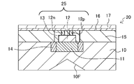
実施形態の発光モジュールの製造方法は、上述の工程に加え、例えば、凹部10R内に透光性部材14を配置する工程(図1B)、光反射部材15で封止した後、光源25の電極を光反射部材15から露出する工程(図1F)、電極に接続する配線層16を形成する工程(図1G)、配線層16を形成した後、光反射部材15及び導光板10を切断する工程(図1H)のいずれか1つ以上を含んでいてもよい。 In addition to the above-described steps, the method for manufacturing a light-emitting module according to the embodiment includes, for example, a step of disposing the translucent member 14 in the recess 10R (FIG. 1B), sealing with the light-reflecting member 15, and then forming the electrode of the light source 25. from the light reflecting member 15 (FIG. 1F), forming a wiring layer 16 connected to the electrodes (FIG. 1G), and cutting the light reflecting member 15 and the light guide plate 10 after forming the wiring layer 16. (FIG. 1H).

(導光板を準備する工程)
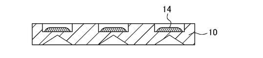
まず、図1Aに示すように、導光板10を準備する。
(Step of preparing light guide plate)
First, as shown in FIG. 1A, a light guide plate 10 is prepared.

(導光板10)
導光板10は、光源からの光が入射され、面状の発光を行うための透光性の部材である。導光板10は、発光面となる第1主面10Uと、第1主面10Uと反対側の第2主面10Bとを備える。
(Light guide plate 10)
The light guide plate 10 is a translucent member that receives light from a light source and emits planar light. The light guide plate 10 has a first main surface 10U that serves as a light emitting surface, and a second main surface 10B opposite to the first main surface 10U.

第2主面10Bには、複数の凹部10Rが配置されている。凹部10Rは、底面と側面と、を備える。凹部10Rの平面視における大きさは、例えば、最大長が0.05mm~10mmとすることができ、0.1mm~1mmが好ましい。深さは0.05mm~4mmとすることができ、0.1mm~1mmが好ましい。凹部10Rの平面視形状は、四角形、五角形等の多角形、円形又は楕円形等が挙げられる。凹部10Rの平面視形状は、四角形又は円形が好ましい。また、凹部10Rの側面は、第1主面又は第2主面に垂直な面、又は、傾斜した面とすることができる。また、凹部10Rの底面は、第1主面又は第2主面に平行な面とすることができる。 A plurality of recesses 10R are arranged on the second main surface 10B. The recess 10R has a bottom surface and side surfaces. The size of the concave portion 10R in plan view can be, for example, a maximum length of 0.05 mm to 10 mm, preferably 0.1 mm to 1 mm. The depth can be from 0.05 mm to 4 mm, preferably from 0.1 mm to 1 mm. The shape of the concave portion 10R in plan view may be polygonal such as a quadrangle or a pentagon, a circle, or an ellipse. The planar shape of the recess 10R is preferably square or circular. Also, the side surface of the recess 10R can be a surface perpendicular to the first principal surface or the second principal surface, or a slanted surface. Also, the bottom surface of the recess 10R can be a surface parallel to the first main surface or the second main surface.

複数の凹部10Rは、行方向又は列方向に等間隔に配置することができる。あるいは、複数の凹部10Rは行方向又は列方向に不等間隔で配置することができる。例えば、複数の凹部10Rは、導光板10の中央から周辺に向かって間隔が広くなるように配列することができる。 The plurality of recesses 10R can be arranged at regular intervals in the row direction or the column direction. Alternatively, the plurality of recesses 10R can be arranged at uneven intervals in the row direction or column direction. For example, the plurality of recesses 10R can be arranged so that the intervals become wider from the center of the light guide plate 10 toward the periphery.

導光板10における凹部10Rの配列ピッチ(最も近接した2つの凹部の間の距離)は、凹部10Rの大きさ、用いる光源の大きさ、特性、得ようとする導光板での輝度等を考慮して適宜調整することができる。例えば、凹部10Rの配列ピッチは、光源の一辺の長さの5倍~20倍が挙げられる。具体的には、0.05mm~20mmとすることができ、2mm~12mmが好ましく、1mm~10mmがより好ましい。 The arrangement pitch (distance between the two closest recesses) of the recesses 10R in the light guide plate 10 takes into consideration the size of the recesses 10R, the size and characteristics of the light source to be used, the luminance to be obtained in the light guide plate, and the like. can be adjusted accordingly. For example, the arrangement pitch of the concave portions 10R may be 5 to 20 times the length of one side of the light source. Specifically, it can be 0.05 mm to 20 mm, preferably 2 mm to 12 mm, and more preferably 1 mm to 10 mm.

導光板10の平面形状は、例えば、多角形、円形等とすることができる。導光板10の大きさは、例えば、一辺が1cm~200cmとすることができ、3cm~30cmが好ましい。導光板10の厚みは0.1mm~5mmとすることができ、0.5mm~3mmが好ましい。 The planar shape of the light guide plate 10 can be, for example, polygonal, circular, or the like. The size of the light guide plate 10 can be, for example, 1 cm to 200 cm on a side, preferably 3 cm to 30 cm. The thickness of the light guide plate 10 can be 0.1 mm to 5 mm, preferably 0.5 mm to 3 mm.

導光板10は、アクリル、ポリカーボネート、環状ポリオレフィン、ポリエチレンテレフタレート若しくはポリエステル等の熱可塑性樹脂、エポキシ樹脂若しくはシリコーン樹脂等の熱硬化性樹脂等の樹脂材料、又はガラスなどの光学的に透明な材料を用いて形成することができる。特に、射出成形によって効率よく製造できるという観点から、熱可塑性の樹脂材料が好ましい。特に、透明性が高く、安価なポリカーボネート、ポリエチレンテレフタレートが好ましい。 The light guide plate 10 is made of thermoplastic resin such as acrylic, polycarbonate, cyclic polyolefin, polyethylene terephthalate or polyester, resin material such as thermosetting resin such as epoxy resin or silicone resin, or optically transparent material such as glass. can be formed by In particular, a thermoplastic resin material is preferable from the viewpoint that it can be efficiently manufactured by injection molding. In particular, polycarbonate and polyethylene terephthalate, which have high transparency and are inexpensive, are preferred.

導光板10は、例えば、射出成形、トランスファ成形等で成形して準備することができる。導光板10の凹部10Rは、導光板10の成形時に凹部10Rも同時に形成することが好ましい。これにより、凹部10Rの位置ずれを低減することができる。導光板10は、購入により準備することができる。また、凹部を備えない平板状の導光板を購入又は成形し、凹部を形成するなどの加工工程を経て準備することができる。 The light guide plate 10 can be prepared by molding, for example, by injection molding, transfer molding, or the like. It is preferable that the concave portion 10R of the light guide plate 10 is formed at the same time when the light guide plate 10 is molded. As a result, it is possible to reduce misalignment of the concave portion 10R. The light guide plate 10 can be prepared by purchase. Alternatively, it is possible to purchase or mold a flat plate-like light guide plate that does not have recesses, and to prepare it through processing steps such as forming recesses.

導光板10は単層で形成されていてもよく、複数の透光性の層が積層されて形成されていてもよい。複数の透光性の層が積層されている場合には、透光性の各層の全面を、接着剤又は接着シートで接合させることができる。あるいは、透光性の層間に、屈折率の異なる層、例えば空気の層等を設けてもよい。これにより、光をより拡散させやすくなり、輝度ムラを低減した発光モジュールとすることができる。このような構成は、例えば、任意の複数の透光性の層の間にスペーサを設けて離間させ、空気の層を設けることで実現することができる。 The light guide plate 10 may be formed of a single layer, or may be formed by laminating a plurality of translucent layers. When a plurality of light-transmitting layers are laminated, the entire surface of each light-transmitting layer can be bonded with an adhesive or an adhesive sheet. Alternatively, a layer having a different refractive index, such as an air layer, may be provided between the translucent layers. As a result, the light can be diffused more easily, and the light-emitting module can have reduced luminance unevenness. Such a structure can be realized, for example, by providing a spacer between arbitrary light-transmitting layers to separate them and providing an air layer.

導光板10は、第1主面10Uに、反射又は拡散機能等を有する光学機能部10Fを備えていてもよい。 The light guide plate 10 may include an optical function portion 10F having a reflecting or diffusing function or the like on the first main surface 10U.

光学機能部10Fは、光を導光板10の面内で広げ、導光板10の面内における発光強度を平均化させる機能を有するものが好ましい。例えば、光学機能部10Fは、第1主面10U側に設けた凹みとすることができる。光学機能部10Fは、例えば、円錐状、四角錐状、六角錐状等の多角錐形等の凹み、円錐台状、四角錘台状又は六角錘台状等の多角錘台状の凹みが挙げられる。 The optical function part 10</b>F preferably has a function of spreading light within the plane of the light guide plate 10 and averaging the emission intensity within the plane of the light guide plate 10 . For example, the optical function part 10F can be a recess provided on the first main surface 10U side. The optical function part 10F includes, for example, a concavity such as a polygonal pyramid shape such as a conical shape, a square pyramid shape, a hexagonal pyramid shape, etc., and a polypyramidal truncated recess such as a truncated cone shape, a square pyramid shape, or a hexagonal truncated pyramid shape. be done.

これらの凹みの内部に、導光板10と屈折率の異なる材料(例えば空気)を配置することで、凹みの側面(傾斜面)との界面に照射された光を光源25の側方方向に反射させることができる。また、凹み内には、光反射性材料(例えば、光反射性の金属、白色樹脂、誘電体膜)等を配置してもよい。 By arranging a material (for example, air) having a different refractive index from that of the light guide plate 10 inside these recesses, the light irradiated to the interface with the side surfaces (inclined surfaces) of the recesses is reflected in the lateral direction of the light source 25. can be made Also, a light-reflecting material (for example, light-reflecting metal, white resin, dielectric film) or the like may be placed in the recess.

光学機能部10Fとして機能する凹みの側面(傾斜面)は、断面視において直線でもよく、曲線でもよい。凹みの側面は、断面視において内側に凸状となる曲面とすることができ、又は、内側に凹状となる曲面とすることができる。また、凹みの側面は、断面視において曲率の異なる曲面を2以上備えていてもよい。上述の光反射性材料は、凹みの側面の、一部又は全部を被覆するように配置することができる。 The side surface (inclined surface) of the recess that functions as the optical function portion 10F may be straight or curved in a cross-sectional view. The side surface of the recess may be curved inwardly convex or curved inwardly when viewed in cross section. Also, the side surface of the recess may have two or more curved surfaces with different curvatures in a cross-sectional view. The light-reflecting material described above can be arranged to cover part or all of the sides of the recess.

光学機能部10Fは、平面視において凹部10Rと重なる位置に設けられていることが好ましい。平面視において光学機能部10Fの中心と、凹部10Rの中心とは一致することが好ましい。 The optical function portion 10F is preferably provided at a position overlapping the recess 10R in plan view. It is preferable that the center of the optical function portion 10F and the center of the recess 10R match in plan view.

導光板10の第1主面10U、第2主面10Bには、凹凸が形成されていてもよい。 Concavities and convexities may be formed on the first main surface 10U and the second main surface 10B of the light guide plate 10 .

(波長変換部材を準備する工程)
図1Aに示すように、波長変換部材11を準備する。波長変換部材11は、導光板の凹部の数と同数以上を準備する。波長変換部材11は、後述の樹脂材料又はガラスと蛍光体とを含む材料を用いて、射出成形、トランスファ成形、印刷等の方法で板状に成形した後、切断する等の工程を経て準備することができる。また、あらかじめ小片の波長変換部材を形成する場合は、切断工程を省略することができる。さらに、蛍光体を含まない、又は、蛍光体を含む板状の樹脂材料又はガラスを準備し、その板状部材の1以上の面に、蛍光体を含む液状の樹脂材料を印刷又はスプレーすることで蛍光体層を形成することによって、波長変換部材を準備することができる。あるいは、蛍光体を含まない、又は、蛍光体を含む板状の樹脂材料又はガラスを準備し、電気泳動により板状部材の表面に蛍光体を付着させることで、波長変換部材を準備することができる。また、板状の波長変換部材を購入し、切断することで準備してもよい。あるいは、小片の波長変換部材を購入することで準備してもよい。
(Step of preparing wavelength conversion member)
As shown in FIG. 1A, a wavelength conversion member 11 is prepared. The number of wavelength conversion members 11 equal to or greater than the number of recesses of the light guide plate is prepared. The wavelength conversion member 11 is prepared using a resin material or a material containing glass and a phosphor, which will be described later, by molding it into a plate shape by a method such as injection molding, transfer molding, or printing, and then cutting the plate. be able to. Moreover, when forming the wavelength conversion member of a small piece beforehand, a cutting process can be abbreviate|omitted. Furthermore, a plate-shaped resin material or glass that does not contain a phosphor or that contains a phosphor is prepared, and a liquid resin material containing a phosphor is printed or sprayed on one or more surfaces of the plate-shaped member. A wavelength conversion member can be prepared by forming a phosphor layer in the above. Alternatively, the wavelength conversion member can be prepared by preparing a plate-shaped resin material or glass that does not contain a fluorescent substance or that contains a fluorescent substance and adheres the fluorescent substance to the surface of the plate-shaped member by electrophoresis. can. Moreover, you may prepare by purchasing and cutting|disconnecting a plate-shaped wavelength conversion member. Alternatively, it may be prepared by purchasing a small piece of wavelength conversion member.

(波長変換部材)
波長変換部材11は、発光素子から出射された光の波長を変換し得る部材であり、例えば、蛍光体又は蛍光体を含有する透光性の材料を含む。波長変換部材11は、エポキシ樹脂、シリコーン樹脂、これらを混合した樹脂、又は、ガラスなどの透光性材料を用いることができる。波長変換部材11の耐光性及び成形容易性の観点からは、シリコーン樹脂が好ましい。波長変換部材11を構成する透光性の材料は、導光板10の材料よりも高い屈折率を有する材料が好ましい。
(Wavelength conversion member)
The wavelength conversion member 11 is a member capable of converting the wavelength of light emitted from the light emitting element, and includes, for example, a phosphor or a translucent material containing a phosphor. The wavelength conversion member 11 can be made of epoxy resin, silicone resin, a resin mixture thereof, or a translucent material such as glass. From the viewpoint of light resistance and moldability of the wavelength conversion member 11, a silicone resin is preferable. A translucent material forming the wavelength conversion member 11 is preferably a material having a higher refractive index than the material of the light guide plate 10 .

波長変換部材11が含有する蛍光体としては、イットリウム・アルミニウム・ガーネット系蛍光体(例えばY(Al,Ga)12:Ce)、ルテチウム・アルミニウム・ガーネット系蛍光体(例えばLu(Al,Ga)12:Ce)、テルビウム・アルミニウム・ガーネット系蛍光体(例えばTb(Al,Ga)12:Ce)系蛍光体、シリケート系蛍光体(例えば(Ba,Sr)SiO:Eu)、クロロシリケート系蛍光体(例えばCaMg(SiOCl:Eu)が挙げられる。さらに、窒化物系蛍光体として、βサイアロン系蛍光体(例えばSi-zAlzOzN-z:Eu(0<z<4.2))、αサイアロン系蛍光体(例えばMz(Si,Al)12(O,N)16(但し、0<z≦2であり、MはLi、Mg、Ca、Y、及びLaとCeを除くランタニド元素)、窒素含有アルミノ珪酸カルシウム(CASN又はSCASN)系蛍光体(例えば(Sr,Ca)AlSiN:Eu)などが挙げられる。一般式(I)MaxMbyAlNz:Euで表される蛍光体(ただし、上記一般式(I))中、Maは、Ca、Sr及びBaからなる群から選択される少なくとも1種の元素であり、Mbは、Li、Na及びKからなる群から選択される少なくとも1種の元素であり、x、y及びzはそれぞれ、0.5≦x≦1.5、0.5≦y≦1.2、及び3.5≦z≦4.5を満たす)、が挙げられる。さらに、SGS系蛍光体(例えばSrGa:Eu)が挙げられる。このほか、マンガン賦活フッ化物系蛍光体(一般式(II)A[M1-aMnaF]で表される蛍光体(但し、上記一般式(II)中、Aは、K、Li、Na、Rb、Cs及びNHからなる群から選ばれる少なくとも1種であり、Mは、第4族元素及び第14族元素からなる群から選ばれる少なくとも1種の元素であり、aは0<a<0.2を満たす))が挙げられる。このマンガン賦活フッ化物系蛍光体の代表例としては、マンガン賦活フッ化珪酸カリウムの蛍光体(例えばKSF(KSiF:Mn))がある。特に、複数種類の波長変換部材を1つの波長変換部材11において用いること、より好ましくは、波長変換部材11が緑色系の発光をするβサイアロン系蛍光体と赤色系の発光をするKSF系蛍光体等のフッ化物系蛍光体とを含むことにより、発光モジュールの色再現範囲を広げることができる。 Phosphors contained in the wavelength conversion member 11 include yttrium - aluminum-garnet-based phosphors (for example, Y3(Al,Ga) 5O12 :Ce), lutetium-aluminum-garnet-based phosphors (for example, Lu3 ( Al , Ga) 5 O 12 :Ce), terbium-aluminum-garnet-based phosphors (for example, Tb 3 (Al, Ga) 5 O 12 :Ce)-based phosphors, silicate-based phosphors (for example, (Ba, Sr) 2 SiO 4 :Eu), and chlorosilicate - based phosphors (for example, Ca8Mg ( SiO4) 4Cl2 :Eu). Furthermore, as nitride phosphors, β-sialon phosphors (eg Si 6 -zAlzOzN 8 -z:Eu (0<z<4.2)), α-sialon phosphors (eg Mz(Si, Al) 12 (O, N) 16 (where 0 < z ≤ 2, and M is a lanthanide element excluding Li, Mg, Ca, Y, and La and Ce), nitrogen-containing calcium aluminosilicate (CASN or SCASN) phosphor (for example, (Sr , Ca) AlSiN 3 :Eu). at least one element selected from the group consisting of Sr and Ba; Mb is at least one element selected from the group consisting of Li, Na and K; x, y and z are each 0; .5≦x≦1.5, 0.5≦y≦1.2, and 3.5≦z≦4.5). Furthermore, an SGS-based phosphor (for example, SrGa 2 S 4 :Eu) can be used. In addition, a manganese-activated fluoride-based phosphor (a phosphor represented by the general formula (II) A 2 [M 1-a MnaF 6 ] (wherein the above general formula (II), A is K, Li, is at least one selected from the group consisting of Na, Rb, Cs and NH4, M is at least one element selected from the group consisting of Group 4 elements and Group 14 elements, and a is 0< satisfies a<0.2)). A representative example of this manganese-activated fluoride-based phosphor is a manganese-activated potassium fluorosilicate phosphor (for example, KSF (K 2 SiF 6 :Mn)). In particular, a plurality of types of wavelength conversion members are used in one wavelength conversion member 11, and more preferably, the wavelength conversion member 11 is composed of a β-sialon phosphor that emits greenish light and a KSF phosphor that emits reddish light. The color reproduction range of the light-emitting module can be widened by including a fluoride-based phosphor such as

波長変換部材11を構成する蛍光体及び/又は透光性材料は、目的とする色度等によって適宜選択し、それらの量を調整することができる。透光性の材料が蛍光体を含む場合、蛍光体は、透光性の材料中に略均一に分布していてもよく、一部に偏在してもよい。また、波長変換部材は、同じ又は異なる蛍光体をそれぞれ同じ又は異なる濃度で含有する複数の層が積層されて形成されていてもよい。 The phosphor and/or translucent material that constitute the wavelength conversion member 11 can be appropriately selected depending on the desired chromaticity and the like, and the amounts thereof can be adjusted. When the translucent material contains a phosphor, the phosphor may be distributed substantially uniformly in the translucent material, or may be unevenly distributed. Also, the wavelength conversion member may be formed by stacking a plurality of layers containing the same or different phosphors at the same or different concentrations.

波長変換部材11には、蛍光体が含有された層と同じ層に、又は、異なる層に、拡散材を含有する層が配置されていてもよい。拡散材としては、SiO、TiO等が挙げられる。 In the wavelength conversion member 11, a layer containing a diffusing material may be arranged in the same layer as the layer containing the phosphor or in a different layer. Examples of diffusion materials include SiO 2 and TiO 2 .

波長変換部材11は、任意の大きさの板状体として、複数準備することが好ましい。波長変換部材11の平面形状は、多角形、円形等とすることができる。波長変換部材11の平面形状は、四角形であることが好ましい。波長変換部材11の大きさは、平面視において、導光板10の凹部10Rよりも面積が小さいものが好ましい。言い換えると、波長変換部材11の外縁の全部が、導光板10の凹部10Rの外縁内に収まる大きさであることが好ましい。特に、波長変換部材11の平面視における面積は、導光板10の凹部10Rの平面視における面積の99%~60%であることが好ましく、95%~80%であることがより好ましい。 It is preferable to prepare a plurality of wavelength conversion members 11 as plate-shaped bodies of arbitrary sizes. The planar shape of the wavelength conversion member 11 can be polygonal, circular, or the like. It is preferable that the planar shape of the wavelength conversion member 11 is a quadrangle. The size of the wavelength converting member 11 is preferably smaller than the area of the concave portion 10R of the light guide plate 10 in plan view. In other words, it is preferable that the entire outer edge of the wavelength conversion member 11 is sized to fit within the outer edge of the concave portion 10</b>R of the light guide plate 10 . In particular, the area of the wavelength converting member 11 in plan view is preferably 99% to 60%, more preferably 95% to 80%, of the area of the concave portion 10R of the light guide plate 10 in plan view.

波長変換部材11の断面形状は、波長変換部材11が、導光板10の凹部10Rに収まる形状とすることができる。例えば、波長変換部材11の断面視形状は、上面が幅狭又は幅広の台形、半円等のいずれでもよい。特に、波長変換部材11の断面視形状は、四角形であることが好ましい。波長変換部材11の厚みは、導光板10の凹部10Rの深さと同じ厚み又は小さい厚みとすることができる。 The cross-sectional shape of the wavelength conversion member 11 can be such that the wavelength conversion member 11 can be accommodated in the concave portion 10</b>R of the light guide plate 10 . For example, the cross-sectional shape of the wavelength conversion member 11 may be trapezoidal, semicircular, or the like with a narrow or wide upper surface. In particular, the cross-sectional shape of the wavelength conversion member 11 is preferably quadrangular. The thickness of the wavelength conversion member 11 can be the same thickness as the depth of the recess 10R of the light guide plate 10 or a thickness smaller than that.

波長変換部材11は、その表面に凹凸が形成されていてもよい。 The wavelength conversion member 11 may have irregularities formed on its surface.

(光源を準備する工程)
図1Aに示すように、光源25を準備する。光源25は、波長変換部材11と同様に、導光板10の凹部10Rの数と同数以上を準備する。光源25は、発光素子12と、被覆部材13とを備える。
(Step of preparing light source)
As shown in FIG. 1A, a light source 25 is provided. As with the wavelength conversion member 11, the number of the light sources 25 equal to or greater than the number of the concave portions 10R of the light guide plate 10 is prepared. Light source 25 includes light emitting element 12 and covering member 13 .

図3A及び図3Bに示す発光モジュールでは、光源25の幅は、波長変換部材11の幅よりも大きい、つまり、平面視において、光源25の外縁は波長変換部材11の外側に配置されている例を示している。また、光源25の幅は、波長変換部材11の幅と同じでもよく、図3Cに示すように、光源25の幅は、波長変換部材11の幅よりも小さくてもよい。 In the light emitting module shown in FIGS. 3A and 3B, the width of the light source 25 is larger than the width of the wavelength conversion member 11, that is, the outer edge of the light source 25 is arranged outside the wavelength conversion member 11 in plan view. is shown. Also, the width of the light source 25 may be the same as the width of the wavelength conversion member 11, or the width of the light source 25 may be smaller than the width of the wavelength conversion member 11 as shown in FIG. 3C.

(発光素子)
発光素子12は、第1面12Uと、第1面の反対側の第2面とを備える半導体積層体と、第2面に配置される電極12n、12pとを備える。発光素子としては、公知の半導体発光素子を利用することができる。例えば、半導体積層体として、サファイア等の透光性基板と、透光性基板の上に積層された半導体層とを有する。半導体層は、発光層と、発光層を挟むn型半導体層及びp型半導体層とを含み、n型半導体層及びp型半導体層に電極12n、12pがそれぞれ電気的に接続される。電極12n、12pは、双方とも、発光素子の半導体積層体の第2面側に配置されている。
(light emitting element)
The light emitting element 12 includes a semiconductor laminate having a first surface 12U and a second surface opposite to the first surface, and electrodes 12n and 12p arranged on the second surface. A known semiconductor light emitting device can be used as the light emitting device. For example, the semiconductor laminate includes a translucent substrate such as sapphire and a semiconductor layer laminated on the translucent substrate. The semiconductor layers include a light emitting layer, and an n-type semiconductor layer and a p-type semiconductor layer sandwiching the light emitting layer. Electrodes 12n and 12p are electrically connected to the n-type semiconductor layer and the p-type semiconductor layer, respectively. Both of the electrodes 12n and 12p are arranged on the second surface side of the semiconductor laminate of the light emitting element.

複数の光源25は、それぞれ異なる色の光を出射する発光素子を備えることができる。又は、複数の光源25は、同じ色の光を出射する発光素子を備えることができる。例えば、青色、緑色の光を出射する発光素子としては、窒化物系半導体(InAlGa1-x-yN、0≦X、0≦Y、X+Y≦1)又はGaPを用いた発光素子を用いることができる。さらに、これら以外の材料からなる半導体発光素子を用いることもできる。半導体層の材料及びその混晶度によって発光波長を種々選択することができる。用いる発光素子の組成、発光色、大きさ、個数などは、目的に応じて適宜選択することができる。 The plurality of light sources 25 can include light emitting elements that emit light of different colors. Alternatively, multiple light sources 25 may comprise light emitting elements that emit light of the same color. For example, as a light-emitting element that emits blue and green light, a nitride-based semiconductor (In x Al y Ga 1-x-y N, 0≦X, 0≦Y, X+Y≦1) or GaP is used for light emission. element can be used. Furthermore, semiconductor light-emitting elements made of materials other than these can also be used. Various emission wavelengths can be selected depending on the material of the semiconductor layer and its crystallinity. The composition, emission color, size, number, and the like of the light-emitting elements to be used can be appropriately selected according to the purpose.

1つの光源25は、1又は2以上の発光素子12を備えることができる。1つの光源25は、同じ色の光を出射する発光素子を備えることができる。あるいは、1つの光源25は、異なる色の光を出射する光を備えることができる。その場合、青色、又は緑色の光を発する発光素子との組み合わせとして、赤色の光を出射する発光素子を用いることができる。赤色の光を出射する発光素子としては、GaAlAs、AlInGaPなどの半導体を含む発光素子を用いることができる。 One light source 25 can comprise one or more light emitting elements 12 . One light source 25 can comprise light emitting elements that emit light of the same color. Alternatively, one light source 25 can comprise lights that emit light of different colors. In that case, a light-emitting element that emits red light can be used in combination with a light-emitting element that emits blue or green light. As a light-emitting element that emits red light, a light-emitting element containing a semiconductor such as GaAlAs or AlInGaP can be used.

発光素子12は、縦、横及び高さの寸法は任意に設定することができる。平面視において縦及び横の寸法が1000μm以下であることが好ましく、500μm以下であることがより好ましい。このような発光素子を用いることにより、例えば、液晶ディスプレイ装置のローカルディミングを行った際に、高精細な映像を実現することができる。また、光源25を安価に調達することができるため、発光モジュール20を安価にすることができる。 The length, width and height of the light emitting element 12 can be arbitrarily set. The vertical and horizontal dimensions in plan view are preferably 1000 μm or less, more preferably 500 μm or less. By using such a light-emitting element, for example, a high-definition image can be realized when local dimming is performed on a liquid crystal display device. In addition, since the light source 25 can be procured at a low cost, the light emitting module 20 can be made at a low cost.

(被覆部材)
被覆部材13は、光源の一部を構成し、発光素子12の半導体積層体の側面を被覆する。さらに、被覆部材13は、発光素子12の電極12n、12pの表面の少なくとも一部が露出するように半導体積層体の第2面を被覆する。被覆部材13は、電極12n、12pの側面の少なくとも一部を被覆する。
(coating member)
The covering member 13 constitutes a part of the light source and covers the side surface of the semiconductor laminate of the light emitting element 12 . Furthermore, the covering member 13 covers the second surface of the semiconductor laminate so that at least part of the surface of the electrodes 12n and 12p of the light emitting element 12 is exposed. The covering member 13 covers at least part of the side surfaces of the electrodes 12n and 12p.

被覆部材13は、光反射性の材料を用いることができる。被覆部材13の反射率は、発光素子から出射される光に対し、例えば、60%以上の反射率を有するものが挙げられ、90%以上の反射率を有するものが挙げられる。光反射性を有する被覆部材13は、例えば、樹脂材料として、熱硬化性樹脂、熱可塑性樹脂などに、光反射性物質を含有するもの等を用いることができる。具体的には、エポキシ樹脂、シリコーン樹脂、シリコーン変性エポキシ樹脂などの変性エポキシ樹脂、エポキシ変性シリコーン樹脂などの変性シリコーン樹脂、不飽和ポリエステル、飽和ポリエステル、ポリイミド樹脂、変性ポリイミド樹脂、ポリフタルアミド(PPA)、ポリカーボネート、ポリフェニレンサルファイド(PPS)、液晶ポリマー(LCP)、ABS樹脂、フェノール樹脂、アクリル樹脂、PBT樹脂等の樹脂を用いることができる。特に、エポキシ樹脂、シリコーン樹脂又は変性シリコーン樹脂の熱硬化性樹脂を用いることが好ましい。光反射性物質としては、酸化チタン、酸化ケイ素、酸化ジルコニウム、チタン酸カリウム、酸化アルミニウム、酸化亜鉛、窒化アルミニウム、窒化ホウ素、ムライトなどを挙げることができる。光反射性物質は、例えば、樹脂の全重量に対して、20重量%~60重量%含有することができる。 A light reflective material can be used for the covering member 13 . The reflectance of the covering member 13 may be, for example, 60% or more, or 90% or more, with respect to the light emitted from the light emitting element. For the light-reflecting covering member 13, for example, a thermosetting resin, a thermoplastic resin, or the like containing a light-reflecting substance can be used as a resin material. Specifically, modified epoxy resins such as epoxy resins, silicone resins, silicone-modified epoxy resins, modified silicone resins such as epoxy-modified silicone resins, unsaturated polyesters, saturated polyesters, polyimide resins, modified polyimide resins, polyphthalamide (PPA) ), polycarbonate, polyphenylene sulfide (PPS), liquid crystal polymer (LCP), ABS resin, phenol resin, acrylic resin, PBT resin, and the like. In particular, it is preferable to use a thermosetting resin such as an epoxy resin, a silicone resin, or a modified silicone resin. Light-reflecting substances include titanium oxide, silicon oxide, zirconium oxide, potassium titanate, aluminum oxide, zinc oxide, aluminum nitride, boron nitride, and mullite. The light-reflecting substance can be contained, for example, in an amount of 20% to 60% by weight with respect to the total weight of the resin.

平面視において、光源25が波長変換部材11と同じ大きさ又は小さい場合、被覆部材13は、透光性の材料を用いることができる。つまり、図3Bに示すように、平面視において、光源25の全てが波長変換部材11と重なる場合、発光素子からの光は、半導体積層体の第1面及び被覆部材から、波長変換部材11に入射される。被覆部材13の透過率は、発光素子から出射される光に対し、例えば、95%以上とすることができる。 When the light source 25 is the same size as or smaller than the wavelength conversion member 11 in plan view, the covering member 13 may be made of a translucent material. That is, as shown in FIG. 3B, when the entire light source 25 overlaps the wavelength conversion member 11 in plan view, the light from the light emitting element is transmitted from the first surface of the semiconductor laminate and the covering member to the wavelength conversion member 11. is incident. The transmittance of the covering member 13 can be, for example, 95% or more with respect to the light emitted from the light emitting element.

被覆部材13は、発光素子12の側面の全部又は一部に接触して被覆することができる。被覆部材13は、図3A等に示すように、発光素子12の側面の全部に接触して被覆することができる。 The covering member 13 can cover all or part of the side surface of the light emitting element 12 in contact therewith. As shown in FIG. 3A and the like, the covering member 13 can contact and cover the entire side surface of the light emitting element 12 .

また、被覆部材13は、図3Bに示すように、透光性接合部材19を介して、発光素子12の側面の一部を被覆していてもよい。この場合の透光性接合部材19は、例えば、外側の側面が発光素子12の側面に対してなだらかな凹面状となるように、発光素子12の側面の一部を被覆することが好ましい。言い換えると、透光性接合部材19の断面視形状は、発光素子12の側面の半導体積層体の第1面側で幅が広く、第2面に向かって徐々に幅が狭くなる形状とすることが好ましい。 3B, the covering member 13 may cover a part of the side surface of the light emitting element 12 via the translucent bonding member 19. As shown in FIG. In this case, the translucent bonding member 19 preferably covers part of the side surface of the light emitting element 12 so that the outer side surface is gently concave with respect to the side surface of the light emitting element 12, for example. In other words, the cross-sectional shape of the translucent bonding member 19 should be such that the width is wide on the first surface side of the semiconductor laminate on the side surface of the light emitting element 12 and gradually narrows toward the second surface. is preferred.

発光素子の半導体積層体の第1面は、透光性の薄膜で覆われていてもよい。透光性の薄膜としては、例えば、前述の波長変換部材に含まれる透光性材料として挙げられた材料と同様の材料を用いることができる。 The first surface of the semiconductor laminate of the light emitting element may be covered with a translucent thin film. As the light-transmitting thin film, for example, the same material as the light-transmitting material included in the wavelength conversion member can be used.

このような光源25は、購入して準備することができる。あるいは、光源25は、発光素子12を形成する工程、発光素子12を被覆部材13で被覆する工程等の少なくとも1つの工程を経て準備することができる。図2A~図2Cに、光源25の製造方法の一例を示す。 Such a light source 25 can be purchased and prepared. Alternatively, the light source 25 can be prepared through at least one process such as the process of forming the light emitting element 12 and the process of covering the light emitting element 12 with the covering member 13 . 2A-2C show an example of a method of manufacturing the light source 25. FIG.

(発光素子を固定する工程)
まず、図2Aに示したように、上述した発光素子12における半導体積層体の第1面(発光面)側を、基材18上に透光性接合材料19aによって固定する。ここで用いる透光性接合材料19aは、透光性を有するもの、例えば、発光素子から出射される光の60%以上を透過する樹脂、70%以上を透過する樹脂が好ましい。透光性接合材料としては、例えば、エポキシ樹脂、シリコーン樹脂又は変性シリコーン樹脂の熱硬化性樹脂を用いることが挙げられる。
(Step of fixing the light emitting element)
First, as shown in FIG. 2A, the first surface (light emitting surface) side of the semiconductor laminate in the light emitting element 12 described above is fixed onto the base material 18 with a translucent bonding material 19a. The translucent bonding material 19a used here preferably has translucency, for example, a resin that transmits 60% or more of the light emitted from the light emitting element, or a resin that transmits 70% or more of the light. As the translucent bonding material, for example, a thermosetting resin such as an epoxy resin, a silicone resin, or a modified silicone resin can be used.

透光性接合材料19aは、ポッティング、印刷等により基材18上に配置することができる。透光性接合材料19aの上に、発光素子12における半導体積層体の第1面を載置する。透光性接合材料19aを加熱して硬化させる。図2Aでは、透光性接合材料19aが発光素子12の側面に這い上がって、発光素子12の側面の一部を覆うように配置されている。ただし、図1Aに示すように、透光性接合材料19aは発光素子12の側面に配置されていなくてもよい。透光性接合材料19aが発光素子12の側面に配置される場合には、発光素子12の側面方向に出射された光を、波長変換部材11及び導光板10の方向に効率よく取り出すことができる。 The translucent bonding material 19a can be arranged on the base material 18 by potting, printing, or the like. The first surface of the semiconductor laminate in the light emitting element 12 is placed on the translucent bonding material 19a. The translucent bonding material 19a is heated and cured. In FIG. 2A , the translucent bonding material 19 a extends over the side surface of the light emitting element 12 and is arranged to partially cover the side surface of the light emitting element 12 . However, as shown in FIG. 1A, the translucent bonding material 19a does not have to be arranged on the side surface of the light emitting element 12 . When the translucent bonding material 19a is arranged on the side surface of the light emitting element 12, the light emitted in the side direction of the light emitting element 12 can be efficiently extracted in the direction of the wavelength conversion member 11 and the light guide plate 10. .

基材18としては、剛性又は柔軟性を有する絶縁材料又は導電材料等のいずれの材料で形成されたものでもよい。例えば、基材18として、樹脂材料、金属材料等が挙げられる。基材18は、安価であり、除去が容易であるという観点から、一方の面に透光性接合材料が塗布された樹脂シート等が好ましい。 The base material 18 may be formed of any material such as an insulating material or a conductive material having rigidity or flexibility. For example, the base material 18 may be a resin material, a metal material, or the like. The base material 18 is preferably a resin sheet or the like having one surface coated with a translucent bonding material from the viewpoint of being inexpensive and easy to remove.

(発光素子を被覆する工程)
次いで、図2Bに示すように、基材18上に固定された発光素子12の発光素子12の全部を被覆するように、被覆部材13aを形成する。その後、図2Cに示すように、被覆部材13aの一部を除去して、発光素子12の電極12n、12pを露出させる。電極12n、12pは少なくとも上面の一部が露出していればよい。被覆部材13aの一部の除去は、研削、エッチング等によって行うことができる。なお、被覆部材13を形成する際に、電極12n、12pの上面を覆わないように形成する場合は、被覆部材13aの一部を除去する工程は省略することができる。
(Step of covering the light emitting element)
Next, as shown in FIG. 2B, a covering member 13a is formed so as to cover all of the light emitting elements 12 of the light emitting elements 12 fixed on the substrate 18. Next, as shown in FIG. Thereafter, as shown in FIG. 2C, a portion of the covering member 13a is removed to expose the electrodes 12n and 12p of the light emitting element 12. Then, as shown in FIG. At least a part of the upper surface of the electrodes 12n and 12p should be exposed. A part of the covering member 13a can be removed by grinding, etching, or the like. When the covering member 13 is formed so as not to cover the upper surfaces of the electrodes 12n and 12p, the step of removing part of the covering member 13a can be omitted.

(基材を除去する工程)
発光素子12の側面を被覆部材13で被覆した後、図2Dに示すように、発光素子12から基材18を除去する。
基材18を除去した後、図2Eに示すように、少なくとも1つの発光素子12を含むように被覆部材13を切断する。また、基材18上で被覆部材13を切断した後、基材18を除去してもよい。
このような方法によって、発光素子12と被覆部材13とを含む光源25を形成することができる。
(Step of removing base material)
After covering the side surface of the light emitting element 12 with the covering member 13, the base material 18 is removed from the light emitting element 12 as shown in FIG. 2D.
After removing the substrate 18, the covering member 13 is cut to include at least one light emitting element 12, as shown in FIG. 2E. Alternatively, the base material 18 may be removed after the covering member 13 is cut on the base material 18 .
By such a method, the light source 25 including the light emitting element 12 and the covering member 13 can be formed.

(凹部内に波長変換部材を配置する工程)
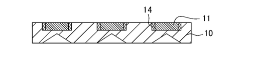
導光板10の凹部10R内に、波長変換部材11を配置する。波長変換部材11は、例えば、透光性部材14によって固定することが好ましい。そのために、図1Bに示すように、まず、導光板10の凹部10R内に、透光性部材14を配置する。透光性部材14は、凹部内ではなく、光源25上に設けてもよい。あるいは、透光性部材14は、凹部10R内及び光源25上の両方に設けてもよい。
(Step of arranging wavelength conversion member in concave portion)
A wavelength converting member 11 is arranged in the concave portion 10</b>R of the light guide plate 10 . The wavelength converting member 11 is preferably fixed by, for example, a translucent member 14 . Therefore, as shown in FIG. 1B, first, the translucent member 14 is arranged in the concave portion 10R of the light guide plate 10 . The translucent member 14 may be provided on the light source 25 instead of inside the recess. Alternatively, the translucent member 14 may be provided both inside the recess 10</b>R and above the light source 25 .

透光性部材14としては、例えば、発光素子から出射される光の60%以上を透過する樹脂、70%以上を透過する樹脂が好ましい。透光性部材14としては、例えば、エポキシ樹脂、シリコーン樹脂、これらを混合した樹脂等が挙げられる。透光性部材14は、透光性及び耐光性等を考慮して、シリコーン樹脂を用いることが好ましい。透光性部材14は、凹部10Rの50%以上の容積、60%以上の容積、95%以下の容積、90%以下の容積で、凹部10R内に配置することが好ましい。透光性部材14を配置する方法としては、ポッティング、転写、スプレー等が挙げられる。 As the translucent member 14, for example, a resin that transmits 60% or more of the light emitted from the light emitting element or a resin that transmits 70% or more of the light is preferable. Examples of the translucent member 14 include epoxy resins, silicone resins, and mixed resins thereof. It is preferable to use a silicone resin for the translucent member 14 in consideration of translucency, light resistance, and the like. The translucent member 14 is preferably arranged in the recess 10R with a volume of 50% or more, 60% or more, 95% or less, or 90% or less of the recess 10R. Potting, transfer, spraying, etc., can be used as a method for disposing the translucent member 14 .

次いで、図1Cに示すように、透光性部材14が配置された凹部10R内に、波長変換部材11を配置する。波長変換部材11は、透光性部材14を介して凹部10Rの底面に固定される。波長変換部材11の一部又は全部は、凹部10R内の透光性部材14に被覆されることが好ましい。また、透光性部材14は、その一部が、凹部10Rの外側の第2主面上に延在してもよい。 Next, as shown in FIG. 1C, the
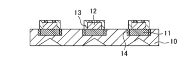
 wavelength converting member 11 is placed inside the recess 10R in which the translucent member 14 is placed. The wavelength conversion member 11 is fixed to the bottom surface of the recess 10R with the translucent member 14 interposed therebetween. Part or all of the wavelength conversion member 11 is preferably covered with the translucent member 14 in the recess 10R. A part of the translucent member 14 may extend on the second main surface outside the recess 10R.

(光源を固定する工程)
続いて、図1Dに示すように、凹部10R内に固定された波長変換部材11の上に、光源25における発光素子12の半導体積層体の第1面を固定する。光源25は、上述した透光性接合部材として用いて波長変換部材11上に固定される。これにより、図3Aに示すように、光源25を波長変換部材11上に固定することができる。
(Step of fixing the light source)
Subsequently, as shown in FIG. 1D, the first surface of the semiconductor laminate of the light emitting element 12 in the light source 25 is fixed on the wavelength conversion member 11 fixed in the recess 10R. The light source 25 is fixed on the wavelength conversion member 11 using as the translucent bonding member described above. Thereby, the light source 25 can be fixed on the wavelength conversion member 11 as shown in FIG. 3A.

また、図3Bに示すように、透光性接合部材19は、透光性部材14の上面の少なくとも一部を被覆してもよい。その場合、透光性接合部材19は、光源25の側面を這い上がるようにしてもよい。詳細には、透光性接合部材19は、光源25の被覆部材13の側面を這い上がる。この場合、透光性接合部材19は、波長変換部材11及び透光性部材14と接するように配置される。透光性接合部材19は、光源25の被覆部材13の側面の各面において、少なくとも一部を被覆することができる。 Further, as shown in FIG. 3B , the translucent bonding member 19 may cover at least a portion of the upper surface of the translucent member 14 . In that case, the translucent joining member 19 may crawl up the side surface of the light source 25 . Specifically, the translucent bonding member 19 crawls up the side surface of the covering member 13 of the light source 25 . In this case, the translucent bonding member 19 is arranged so as to be in contact with the wavelength conversion member 11 and the translucent member 14 . The translucent bonding member 19 can cover at least a portion of each side surface of the covering member 13 of the light source 25 .

このように、導光板10の凹部10R内に波長変換部材11を固定した後、その波長変換部材11上に光源25を固定することにより、光源25の光軸を、凹部10R及び/又は波長変換部材11の所望の位置に配置することができる。その結果、色ずれを効果的に防止することができる。 After fixing the wavelength converting member 11 in the concave portion 10R of the light guide plate 10 in this way, by fixing the light source 25 on the wavelength converting member 11, the optical axis of the light source 25 is aligned with the concave portion 10R and/or the wavelength converting portion. It can be arranged at a desired position on the member 11 . As a result, color misregistration can be effectively prevented.

光源25の配列ピッチは、上述した導光板10の凹部10Rの位置と同じピッチとすることができる。あるいは、導光板の第1面又は第2面における凹部10Rの位置に応じて、凹部のピッチと異なる配列ピッチで配置することができる。例えば、光源25間の距離は、0.05mm~20mmとすることができ、2mm~12mmが好ましく、1mm~10mmがより好ましい。このような配列ピッチとすることで、導光板10の面内において均一な輝度を確保することができる。 The arrangement pitch of the light sources 25 can be the same pitch as the positions of the concave portions 10R of the light guide plate 10 described above. Alternatively, according to the position of the recesses 10R on the first surface or the second surface of the light guide plate, they can be arranged at an arrangement pitch different from the pitch of the recesses. For example, the distance between light sources 25 can be 0.05 mm to 20 mm, preferably 2 mm to 12 mm, more preferably 1 mm to 10 mm. With such an arrangement pitch, it is possible to ensure uniform brightness in the plane of the light guide plate 10 .

(光反射部材で封止する工程)
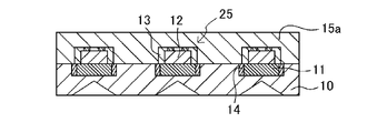
図1Eに示すように、光源25と導光板10の第2主面10Bとを光反射部材15aで封止する。また、導光板10の第2主面10Bも、光反射部材15aで封止する。ここでは、光源25の電極12n、12pの上面も覆うように光反射部材15aを形成する。
(Step of sealing with a light reflecting member)
As shown in FIG. 1E, the light source 25 and the second main surface 10B of the light guide plate 10 are sealed with the light reflecting member 15a. The second main surface 10B of the light guide plate 10 is also sealed with the light reflecting member 15a. Here, the light reflecting member 15a is formed so as to also cover the upper surfaces of the electrodes 12n and 12p of the light source 25. As shown in FIG.

次に、図1Fに示すように、光反射部材15aの一部を除去して、発光素子12の電極12n、12p表面を露出させる。なお、あらかじめ電極の上面を埋めないように光反射部材15を形成する場合は、光反射部材15の一部を除去する工程は省略することができる。光反射部材15と電極12n、12pとは、面一であることが好ましい。 Next, as shown in FIG. 1F, part of the light reflecting member 15a is removed to expose the surfaces of the electrodes 12n and 12p of the light emitting element 12. Next, as shown in FIG. If the light reflecting member 15 is formed so as not to fill the upper surface of the electrode in advance, the step of removing part of the light reflecting member 15 can be omitted. The light reflecting member 15 and the electrodes 12n and 12p are preferably flush with each other.

光反射部材15、15aは、樹脂材料及び光反射性物質等によって形成することができる。例えば、酸化チタンが混合されたシリコーン樹脂が挙げられる。光反射部材15は、例えば、トランスファーモールド、ポッティング、印刷、スプレー等の方法で形成することができる。厚み方向の一部の除去は、研削、エッチング等、当該分野で公知の方法によって行うことができる。 The light reflecting members 15 and 15a can be made of a resin material, a light reflecting substance, or the like. For example, a silicone resin mixed with titanium oxide can be mentioned. The light reflecting member 15 can be formed by transfer molding, potting, printing, spraying, or the like, for example. Partial removal in the thickness direction can be performed by methods known in the art, such as grinding and etching.

(配線層を形成する工程)
次に、発光素子12の電極12n、12pと電気的に接続される配線層16を形成する。例えば、電極12n、12pの上面と光反射部材15の上面とを含む略全面に、スパッタ等により金属膜を形成する。その後、レーザ光を照射することで金属膜の一部を除去することで、所望の形状の配線層16を形成することができる。また、マスク等を用いて導電ペーストを印刷することで所望の形状の配線層16を形成することができる。
(Step of forming wiring layer)
Next, a wiring layer 16 electrically connected to the electrodes 12n and 12p of the light emitting element 12 is formed. For example, a metal film is formed on substantially the entire surface including the upper surfaces of the electrodes 12n and 12p and the upper surface of the light reflecting member 15 by sputtering or the like. After that, the wiring layer 16 having a desired shape can be formed by removing part of the metal film by irradiating it with a laser beam. Moreover, the wiring layer 16 having a desired shape can be formed by printing the conductive paste using a mask or the like.

配線層としては、例えば、Au、Pt、Pd、Rh、Ni、W、Mo、Cr、Ti等の金属又はこれらの合金の単層膜又は積層膜が挙げられる。具体的には、導光板10側からCu/Ni/Auの金属膜等が挙げられる。 Examples of the wiring layer include single-layer films or laminated films of metals such as Au, Pt, Pd, Rh, Ni, W, Mo, Cr, and Ti, or alloys thereof. Specifically, metal films of Cu/Ni/Au from the light guide plate 10 side can be used.

続いて、図1Gに示すように、配線層16と、別途準備した配線基板17の配線層とを圧着して接合し、配線層16と、配線基板17の配線層とを電気的に接続する。これによって、配線基板17と光源25とを電気的に接続することができる。 Subsequently, as shown in FIG. 1G, the wiring layer 16 and the wiring layer of the wiring board 17 prepared separately are pressure-bonded to be joined to electrically connect the wiring layer 16 and the wiring layer of the wiring board 17. . Thereby, the wiring board 17 and the light source 25 can be electrically connected.

配線基板17の母材は、例えば、窒化アルミ等のセラミックス、樹脂等を用いて形成することができる。樹脂としては、フェノール樹脂、エポキシ樹脂、ポリイミド樹脂、BTレジン、ポリフタルアミド(PPA)、ポリエチレンテレフタレート(PET)、不飽和ポリエステル、ガラスエポキシ等の複合材料等が挙げられる。配線基板17は、リジッド基板であってもよく、フレキシブル基板であってもよい。 The base material of the wiring board 17 can be formed using, for example, ceramics such as aluminum nitride, resin, or the like. Examples of resins include composite materials such as phenol resin, epoxy resin, polyimide resin, BT resin, polyphthalamide (PPA), polyethylene terephthalate (PET), unsaturated polyester, and glass epoxy. The wiring board 17 may be a rigid board or a flexible board.

配線層16は、複数の光源25が、それぞれが独立して点灯するように形成することができる。また、導光板10を、複数の光源25が同時に点灯して1つの発光領域となるように、配線層16を形成することができる。例えば、行列状に配置された光源25を、2行2列に配置された4つの光源グループとし、グループごとに発光する配線層を形成することにより、ローカルディミング可能な発光モジュールとすることができる。 The wiring layer 16 can be formed so that the plurality of light sources 25 are individually lit. Further, the wiring layer 16 can be formed on the light guide plate 10 so that a plurality of light sources 25 are turned on at the same time to form one light emitting area. For example, the light sources 25 arranged in a matrix form are divided into four light source groups arranged in two rows and two columns, and a wiring layer that emits light is formed for each group, so that a light emitting module capable of local dimming can be obtained. .

(導光板を切断する工程)
任意に、図1Hに示すように、少なくとも1以上の光源25を含むように、導光板10を切断することができる。また、切断位置に光反射部材15又は配線基板17がある場合は、これらも導光板10と同時に切断することができる。また、あらかじめ所定の形状及び大きさの導光板10を準備する場合は、導光板10を切断する工程は省略することができる。
(Step of cutting the light guide plate)
Optionally, the light guide plate 10 can be cut to include at least one or more light sources 25, as shown in FIG. 1H. Also, if the light reflecting member 15 or the wiring board 17 is present at the cutting position, these can be cut at the same time as the light guide plate 10 is cut. Further, when the light guide plate 10 having a predetermined shape and size is prepared in advance, the step of cutting the light guide plate 10 can be omitted.

〔発光モジュール〕
本実施形態の発光モジュール20を図3Bに示す。
発光モジュール20は、
第1主面10Uと第2主面10Bとを備え、第2主面10Bに凹部10Rを有する導光板10と、
導光板10の第2主面10B側の凹部10R内に配置された波長変換部材11と、
波長変換部材11に接合される光源25であって、発光素子12と、発光素子12の側面を被覆する被覆部材13とを備える光源25と、
導光板10の第2主面10Bと光源25とを封止する光反射部材15と、
光源25と光反射部材15との間に配置され、光源25の側面の一部を被覆する透光性部材(第2透光性部材14a)とを備える。
発光モジュール20は、平面視において、光源25の外縁が波長変換部材11の外縁に配置されている。詳細には、被覆部材13の外縁が波長変換部材11の外側に配置されている。
[Light-emitting module]
The light emitting module 20 of this embodiment is shown in FIG. 3B.
The light emitting module 20 is
a light guide plate 10 having a first principal surface 10U and a second principal surface 10B, and having a concave portion 10R in the second principal surface 10B;
a wavelength conversion member 11 arranged in a recess 10R on the second main surface 10B side of the light guide plate 10;
a light source 25 joined to the wavelength conversion member 11, the light source 25 including the light emitting element 12 and the covering member 13 covering the side surface of the light emitting element 12;
a light reflecting member 15 that seals the second main surface 10B of the light guide plate 10 and the light source 25;
A translucent member (second translucent member 14 a ) is provided between the light source 25 and the light reflecting member 15 and covers a part of the side surface of the light source 25 .
In the light emitting module 20, the outer edge of the light source 25 is arranged on the outer edge of the wavelength conversion member 11 in plan view. Specifically, the outer edge of the covering member 13 is arranged outside the wavelength conversion member 11 .

また、発光モジュール20は、光源25の電極12n、12pと接続された配線層16をさらに備える。 The light emitting module 20 further includes wiring layers 16 connected to the electrodes 12 n and 12 p of the light source 25 .

1つの導光板10は複数の凹部10Rを有し、凹部10Rのそれぞれにおいて、1つの波長変換部材11と、1つの光源25とが配置される。 One light guide plate 10 has a plurality of recesses 10R, and one wavelength conversion member 11 and one light source 25 are arranged in each of the recesses 10R.

このような構成の発光モジュール20とすることで、発光素子からの光をより均一に横方向に広げることができる。平面視において、被覆部材の外縁が波長変換部材の外側に配置されていることで、波長変換部材に入射した光を、導光板に効率的に入光させることができる。そのため、発光モジュールの色ずれを低減することができる。 With the light-emitting module 20 having such a configuration, the light from the light-emitting elements can be spread more uniformly in the lateral direction. In a plan view, the outer edge of the covering member is arranged outside the wavelength conversion member, so that the light that has entered the wavelength conversion member can be efficiently made to enter the light guide plate. Therefore, it is possible to reduce the color shift of the light emitting module.

発光モジュール20は、例えば、図4Bに示すように、液晶ディスプレイ装置30に利用することができる。液晶ディスプレイ装置30は、上側から順に、液晶パネル21、レンズシート22、23、拡散シート24、発光モジュール20を備える。この液晶ディスプレイ装置30は、液晶パネル21の下方に発光モジュール20が配置された、いわゆる直下型の液晶ディスプレイ装置である。液晶ディスプレイ装置30は、発光モジュール20から照射される光を、液晶パネル21に照射する。液晶ディスプレイ装置30は、さらに偏光フィルム、カラーフィルタ等の部材を備えてもよい。 The light emitting module 20 can be used, for example, in a liquid crystal display device 30, as shown in FIG. 4B. The liquid crystal display device 30 includes a liquid crystal panel 21, lens sheets 22 and 23, a diffusion sheet 24, and a light emitting module 20 in order from the top. The liquid crystal display device 30 is a so-called direct type liquid crystal display device in which the light emitting module 20 is arranged below the liquid crystal panel 21 . The liquid crystal display device 30 irradiates the liquid crystal panel 21 with light emitted from the light emitting module 20 . The liquid crystal display device 30 may further include members such as polarizing films and color filters.

10 導光板
10B 第2主面
10F、10F1 光学機能部
10R 凹部
10U 第1主面
11 波長変換部材
12 発光素子
12n 電極
12p 電極
12U 第1面
13、13a 被覆部材
14 透光性部材
14a 第2透光性部材
15、15a 光反射部材
16 配線層
17 配線基板
18 基材
19 透光性接合部材
19a 透光性接合材料
20 発光モジュール
21 液晶パネル
22、23 レンズシート
24 拡散シート
25 光源
30 液晶ディスプレイ装置
REFERENCE SIGNS LIST 10 light guide plate 10B second main surface 10F, 10F1 optical function portion 10R recess 10U first main surface 11 wavelength conversion member 12 light emitting element 12n electrode 12p electrode 12U first surface 13, 13a coating member 14 translucent member 14a second translucent Optical member 15, 15a Light reflecting member 16 Wiring layer 17 Wiring board 18 Base material 19 Translucent bonding member 19a Translucent bonding material 20 Light emitting module 21 Liquid crystal panel 22, 23 Lens sheet 24 Diffusion sheet 25 Light source 30 Liquid crystal display device

Claims (7)

発光面となる第1主面と、前記第1主面の反対側であって、複数の凹部を備える第2主面を有する導光板を準備する工程と、
平面視において、前記凹部の面積よりも小さい面積の波長変換部材を準備する工程と、
第1面と該第1面の反対側の第2面とを備える半導体積層体及び前記第2面に配置される電極を備える発光素子と、前記発光素子の側面を被覆し、前記電極を露出する被覆部材とを備える光源を準備する工程と、
前記凹部内に、前記波長変換部材の側面を被覆するように、透光性部材及び前記波長変換部材を配置する工程と、
前記波長変換部材上に、前記発光素子における前記半導体積層体の前記第1面側を対向させて前記光源を固定する工程と、
前記光源と前記導光板の前記第2主面とを光反射部材で封止する工程と、を含む発光モジュールの製造方法。
preparing a light guide plate having a first main surface serving as a light emitting surface and a second main surface opposite to the first main surface and having a plurality of recesses;
preparing a wavelength conversion member having an area smaller than the area of the recess in plan view;
A light-emitting element comprising a semiconductor laminate having a first surface and a second surface opposite to the first surface and an electrode disposed on the second surface; and covering a side surface of the light-emitting element and exposing the electrode. providing a light source comprising a covering member for
disposing a translucent member and the wavelength conversion member in the recess so as to cover the side surface of the wavelength conversion member;
a step of fixing the light source on the wavelength conversion member with the first surface side of the semiconductor laminate of the light emitting element facing each other;
and sealing the light source and the second main surface of the light guide plate with a light reflecting member.
前記光反射部材で封止した後、前記発光素子の前記電極を前記光反射部材から露出し、前記電極に接続する配線層を形成する工程を備える、請求項1に記載の発光モジュールの製造方法。 2. The method of manufacturing a light-emitting module according to claim 1 , further comprising, after sealing with the light-reflecting member, exposing the electrode of the light-emitting element from the light-reflecting member and forming a wiring layer connected to the electrode. . 前記配線層を形成した後、前記光反射部材及び前記導光板を切断する工程を備える、請求項に記載の発光モジュールの製造方法。 3. The method of manufacturing a light-emitting module according to claim 2 , further comprising cutting the light reflecting member and the light guide plate after forming the wiring layer. 前記発光素子を準備する工程は、
基材上に透光性接合材料によって前記発光素子における前記半導体積層体の第1面を固定する工程と、
前記電極が前記被覆部材から露出するように前記発光素子の側面に前記被覆部材を被覆する工程と、
前記基材を前記発光素子から除去する工程と、を備える請求項1~請求項のいずれか1項に記載の発光モジュールの製造方法。
The step of preparing the light emitting device includes:
a step of fixing the first surface of the semiconductor laminate in the light emitting device onto a base material with a translucent bonding material;
covering the side surface of the light emitting element with the covering member so that the electrode is exposed from the covering member;
The method of manufacturing a light-emitting module according to any one of claims 1 to 3 , further comprising a step of removing the base material from the light-emitting element.
発光面となる第1主面と、前記第1主面の反対側であって、複数の凹部を備える第2主面を有する導光板と、
前記導光板の前記凹部内に配置された波長変換部材と、
該波長変換部材に接合された光源であって、発光素子と、該発光素子の側面を被覆する被覆部材と、を備える光源と、
前記導光板の前記第2主面と前記光源とを封止する光反射部材と、
前記被覆部材と前記光反射部材との間に配置され、前記光源の側面の一部を被覆する透光性接合部材とを備え、
平面視において、前記光源の外縁が前記波長変換部材の外側に配置されてなる発光モジュール。
a light guide plate having a first main surface serving as a light emitting surface and a second main surface opposite to the first main surface and having a plurality of recesses;
a wavelength conversion member disposed within the recess of the light guide plate;
a light source joined to the wavelength conversion member, the light source including a light emitting element and a covering member covering the side surface of the light emitting element;
a light reflecting member that seals the second main surface of the light guide plate and the light source;
a translucent joining member disposed between the covering member and the light reflecting member and covering a part of a side surface of the light source;
A light-emitting module in which an outer edge of the light source is arranged outside the wavelength conversion member in plan view.
前記光源の電極と接続された配線層をさらに備える請求項に記載の発光モジュール。 6. The light emitting module according to claim 5 , further comprising a wiring layer connected to the electrodes of said light source. 1つの前記導光板は複数の凹部を有し、
前記凹部のそれぞれにおいて、
1つの前記波長変換部材と、1つの前記発光素子とが配置される請求項又は請求項に記載の発光モジュール。
one said light guide plate has a plurality of recesses,
in each of the recesses,
7. The light-emitting module according to claim 5 , wherein one said wavelength conversion member and one said light-emitting element are arranged.
JP2020025027A 2020-02-18 2020-02-18 Light-emitting module manufacturing method and light-emitting module Active JP7148810B2 (en)

Priority Applications (1)

Application Number Priority Date Filing Date Title
JP2020025027A JP7148810B2 (en) 2020-02-18 2020-02-18 Light-emitting module manufacturing method and light-emitting module

Applications Claiming Priority (1)

Application Number Priority Date Filing Date Title
JP2020025027A JP7148810B2 (en) 2020-02-18 2020-02-18 Light-emitting module manufacturing method and light-emitting module

Publications (2)

Publication Number Publication Date
JP2021131932A JP2021131932A (en) 2021-09-09
JP7148810B2 true JP7148810B2 (en) 2022-10-06

Family

ID=77551151

Family Applications (1)

Application Number Title Priority Date Filing Date
JP2020025027A Active JP7148810B2 (en) 2020-02-18 2020-02-18 Light-emitting module manufacturing method and light-emitting module

Country Status (1)

Country Link
JP (1) JP7148810B2 (en)

Citations (3)

* Cited by examiner, † Cited by third party
Publication number Priority date Publication date Assignee Title
JP2019220405A (en) 2018-06-22 2019-12-26 日亜化学工業株式会社 Manufacturing method of light emitting module
JP2020009906A (en) 2018-07-09 2020-01-16 日亜化学工業株式会社 Manufacturing method of light emitting module
CN110794614A (en) 2018-08-03 2020-02-14 日亚化学工业株式会社 Light emitting module

Patent Citations (3)

* Cited by examiner, † Cited by third party
Publication number Priority date Publication date Assignee Title
JP2019220405A (en) 2018-06-22 2019-12-26 日亜化学工業株式会社 Manufacturing method of light emitting module
JP2020009906A (en) 2018-07-09 2020-01-16 日亜化学工業株式会社 Manufacturing method of light emitting module
CN110794614A (en) 2018-08-03 2020-02-14 日亚化学工业株式会社 Light emitting module

Also Published As

Publication number Publication date
JP2021131932A (en) 2021-09-09

Similar Documents

Publication Publication Date Title
KR102215923B1 (en) Manufacturing method for light emitting module and light emitting module
CN108459437B (en) Method for manufacturing light emitting module and light emitting module
JP7456858B2 (en) Light Emitting Module
JP6680349B1 (en) Light emitting module
CN116027476A (en) Light emitting module
JP2020107584A (en) Light-emitting module
JP6717351B2 (en) Method for manufacturing light emitting module
JP7116331B2 (en) Light-emitting module manufacturing method and light-emitting module
JP7007591B2 (en) Luminous module
JP2020072269A (en) Light emitting device, light emitting module, and method for manufacturing light emitting device and light emitting module
JP6717400B2 (en) Light emitting module
JP6963183B2 (en) Manufacturing method of light emitting module
JP7148810B2 (en) Light-emitting module manufacturing method and light-emitting module
JP7111993B2 (en) Method for manufacturing light-emitting module
US11181772B2 (en) Light-emitting module, method for manufacturing the same, and liquid-crystal display device
JP2020021910A (en) Method of manufacturing light-emitting module and light-emitting module
JP7239839B2 (en) light emitting module
JP7140987B2 (en) Light-emitting module and method for manufacturing light-emitting module
JP7121298B2 (en) Method for manufacturing linear light source
US11581460B2 (en) Light emitting module and method for manufacturing light emitting module
JP7068594B2 (en) Light emitting module manufacturing method and light emitting module
JP7116327B2 (en) Light-emitting module and method for manufacturing light-emitting module
CN114122229A (en) Light emitting device, method for manufacturing the same, planar light source, and liquid crystal display device
JP2021125371A (en) Manufacturing method of light emitting module
CN115480422A (en) Partition member, planar light source, and liquid crystal display device

Legal Events

Date Code Title Description
A621 Written request for application examination

Free format text: JAPANESE INTERMEDIATE CODE: A621

Effective date: 20210409

A977 Report on retrieval

Free format text: JAPANESE INTERMEDIATE CODE: A971007

Effective date: 20220225

A131 Notification of reasons for refusal

Free format text: JAPANESE INTERMEDIATE CODE: A131

Effective date: 20220301

A521 Request for written amendment filed

Free format text: JAPANESE INTERMEDIATE CODE: A523

Effective date: 20220411

TRDD Decision of grant or rejection written
A01 Written decision to grant a patent or to grant a registration (utility model)

Free format text: JAPANESE INTERMEDIATE CODE: A01

Effective date: 20220823

A61 First payment of annual fees (during grant procedure)

Free format text: JAPANESE INTERMEDIATE CODE: A61

Effective date: 20220905

R151 Written notification of patent or utility model registration

Ref document number: 7148810

Country of ref document: JP

Free format text: JAPANESE INTERMEDIATE CODE: R151