EP2704009A2 - Appareil de traitement d' informations, procédé et programme de traitement d'informations - Google Patents
Appareil de traitement d' informations, procédé et programme de traitement d'informations Download PDFInfo
- Publication number
- EP2704009A2 EP2704009A2 EP20130175508 EP13175508A EP2704009A2 EP 2704009 A2 EP2704009 A2 EP 2704009A2 EP 20130175508 EP20130175508 EP 20130175508 EP 13175508 A EP13175508 A EP 13175508A EP 2704009 A2 EP2704009 A2 EP 2704009A2
- Authority
- EP
- European Patent Office
- Prior art keywords
- data
- interrupt
- computing device
- processing unit
- storage area
- Prior art date
- Legal status (The legal status is an assumption and is not a legal conclusion. Google has not performed a legal analysis and makes no representation as to the accuracy of the status listed.)
- Granted
Links
- 230000010365 information processing Effects 0.000 title claims abstract description 67
- 238000003672 processing method Methods 0.000 title claims description 9
- 230000005540 biological transmission Effects 0.000 claims abstract description 151
- 238000012545 processing Methods 0.000 claims abstract description 135
- 238000013500 data storage Methods 0.000 claims description 11
- 238000007726 management method Methods 0.000 claims 2
- 230000015654 memory Effects 0.000 description 45
- 238000010586 diagram Methods 0.000 description 18
- 238000000034 method Methods 0.000 description 12
- 238000005192 partition Methods 0.000 description 8
- 238000004891 communication Methods 0.000 description 7
- 230000006870 function Effects 0.000 description 7
- 230000000694 effects Effects 0.000 description 3
- 238000005516 engineering process Methods 0.000 description 3
- 230000003287 optical effect Effects 0.000 description 2
- 238000012546 transfer Methods 0.000 description 2
- 238000004590 computer program Methods 0.000 description 1
- 239000000470 constituent Substances 0.000 description 1
- 230000003247 decreasing effect Effects 0.000 description 1
- 238000012986 modification Methods 0.000 description 1
- 230000004048 modification Effects 0.000 description 1
- 230000002093 peripheral effect Effects 0.000 description 1
- 238000011084 recovery Methods 0.000 description 1
- 230000003936 working memory Effects 0.000 description 1
Images


Classifications
-
- G—PHYSICS
- G06—COMPUTING; CALCULATING OR COUNTING
- G06F—ELECTRIC DIGITAL DATA PROCESSING
- G06F9/00—Arrangements for program control, e.g. control units
- G06F9/06—Arrangements for program control, e.g. control units using stored programs, i.e. using an internal store of processing equipment to receive or retain programs
- G06F9/46—Multiprogramming arrangements
- G06F9/48—Program initiating; Program switching, e.g. by interrupt
- G06F9/4806—Task transfer initiation or dispatching
- G06F9/4812—Task transfer initiation or dispatching by interrupt, e.g. masked
-
- G—PHYSICS
- G06—COMPUTING; CALCULATING OR COUNTING
- G06F—ELECTRIC DIGITAL DATA PROCESSING
- G06F13/00—Interconnection of, or transfer of information or other signals between, memories, input/output devices or central processing units
- G06F13/14—Handling requests for interconnection or transfer
- G06F13/20—Handling requests for interconnection or transfer for access to input/output bus
- G06F13/28—Handling requests for interconnection or transfer for access to input/output bus using burst mode transfer, e.g. direct memory access DMA, cycle steal
-
- G—PHYSICS
- G06—COMPUTING; CALCULATING OR COUNTING
- G06F—ELECTRIC DIGITAL DATA PROCESSING
- G06F13/00—Interconnection of, or transfer of information or other signals between, memories, input/output devices or central processing units
- G06F13/14—Handling requests for interconnection or transfer
- G06F13/20—Handling requests for interconnection or transfer for access to input/output bus
- G06F13/24—Handling requests for interconnection or transfer for access to input/output bus using interrupt
-
- G—PHYSICS
- G06—COMPUTING; CALCULATING OR COUNTING
- G06F—ELECTRIC DIGITAL DATA PROCESSING
- G06F13/00—Interconnection of, or transfer of information or other signals between, memories, input/output devices or central processing units
- G06F13/14—Handling requests for interconnection or transfer
- G06F13/20—Handling requests for interconnection or transfer for access to input/output bus
- G06F13/32—Handling requests for interconnection or transfer for access to input/output bus using combination of interrupt and burst mode transfer
- G06F13/34—Handling requests for interconnection or transfer for access to input/output bus using combination of interrupt and burst mode transfer with priority control
-
- G—PHYSICS
- G06—COMPUTING; CALCULATING OR COUNTING
- G06F—ELECTRIC DIGITAL DATA PROCESSING
- G06F9/00—Arrangements for program control, e.g. control units
- G06F9/06—Arrangements for program control, e.g. control units using stored programs, i.e. using an internal store of processing equipment to receive or retain programs
- G06F9/46—Multiprogramming arrangements
- G06F9/54—Interprogram communication
- G06F9/544—Buffers; Shared memory; Pipes
Definitions
- the embodiments discussed herein are directed to an information processing apparatus, an information processing method, and a program.
- a CPU of a transmission source writes data in a share memory of a transmission destination and thereafter, generates and notifies an interrupt to a CPU of the transmission destination.
- the CPU that receives the interrupt accesses the share memory to read out the data written in the memory.
- data communications performed among the CPUs may be called a cross call (xcall).
- BB building block
- BB building block
- the CPU of the transmission destination can efficiently judge from which CPU included in the BB the interrupt is received.
- a cross access competition in which data is transmitted to the same CPU from the CPUs of the plurality of BBs may occur, but in this case, it is desirable to prevent only processing of a specific BB from being prioritized.
- an object of the invention is to efficiently perform communications between computing devices in an information processing apparatus including a plurality of computing devices.
- the invention is not limited to the object, but another object of the invention is to exhibit an operational effect which may not be acquired by the related art, as an operational effect induced by each component described in embodiments for implementing the invention to be described below.
- an information processing apparatus includes: a plurality of computing devices; and a plurality of storage areas, and a first computing device among the plurality of computing devices includes a data transmission processing unit storing data to be transferred to another computing device in a first storage area among the plurality of storage areas, and an interrupt generating unit generating an interrupt corresponding to storage of data by the data transmission processing unit with respect to a transmission destination of the data together with identification information specifying the storage area, and a second computing device among the plurality of computing devices includes an interrupt processing unit specifying from which computing device the interrupt is requested based on the identification information received together with the interrupt when receiving the interrupt, and a data receiving unit reading out data from the first storage area corresponding to the computing device specified by the interrupt processing unit among the plurality of storage areas.
- an information processing method in an information processing apparatus including a plurality of computing devices and a plurality of storage areas, includes: by a first computing device among the plurality of computing devices, transmitting data to be transferred to another computing device to a first storage area among the plurality of storage areas; generating an interrupt corresponding to transmission of the data with respect to a transmission destination of the data together with identification information specifying the storage area, and by a second computing device among the plurality of computing devices, specifying from which computing device the interrupt is requested based on the identification information received together with the interrupt when receiving the interrupt; and reading out data from the first storage area corresponding to the computing device specified by an interrupt processing unit among the plurality of storage areas.
- a program stored therein allows a computer including a plurality of computing devices and a plurality of storage areas to execute processing including: transmitting data to be transferred to another computing device to a first storage area among the plurality of storage areas; and generating an interrupt corresponding to transmission of the data with respect to a transmission destination of the data together with identification information specifying the storage area.
- the communications between the computing devices in the information processing apparatus including the plurality of computing devices can be efficiently performed.
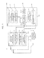
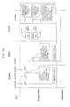
- Fig. 1 is a diagram schematically illustrating a functional configuration of an information processing apparatus 1 as one example of a first embodiment.
- Fig. 2 is a diagram exemplifying a hardware configuration of the information processing apparatus.
- the information processing apparatus 1 includes a plurality of (sixteen of #0 to #15, in the example illustrated in Fig. 2 ) building blocks (BB) 100, as illustrated in Fig. 2 .
- the plurality of BBs #0 to #15 are connected to communicate with each other through a bus 50.
- the BB is one of hardware configuring units and configures a node (computer node).
- the plurality of BBs 100 are, for example, system boards, and the like and has the same configuration as each other.
- Fig. 2 illustrates only a hardware configuration of a BB #0, for convenience.
- the configuration of the BB or the node is not limited to the configuration of Fig. 2 and may include various configurations.
- the configuration of the BB or the node may be a configuration without a service processor 105, and a plurality of CPUs 101 or a plurality of memories 102 connected to a bus interface 104 may be placed on one system board or a function block including a plurality of circuit boards in which the CPU or the memory is installed may be set as the BB or the node.
- the BB 100 includes the service processor 105, the bus interface 104, one or more (four of #0 to #3 in the example illustrated in Fig. 2 ) CPUs 101, one or more (four in the example illustrated in Fig. 2 ) memory access controllers (MACs) 103, and one or more (four in the example illustrated in Fig. 2 ) memories 102.
- Each of the CPU 101 and the memory 102 is connected to the bus interface 104 through the MAC 103. Further, the bus interface 104 is connected to communicate with the bus 50.
- the bus 50 is, for example, a cross bar. However, the bus 50 is not limited thereto and may be, for example, another bus architecture such as a peripheral component interconnect (PCI) bus, or the like.
- PCI peripheral component interconnect
- the bus interface 104 is an interface which conforms to a standard of the bus 50 and for example, a cross bar interface.
- the service processor 105 is a processing device that manages the BB 100, and for example, monitors an error in the BB 100 and performs notification to the outside or recovery processing when the error occurs.
- the MAC 103 is a control device that controls data access to the memory 102 and writes or reads out data in or to the memory 102 in accordance with a data access request from the CPU 101, or the like.
- the memory 102 is a storage device including a ROM and a RAM. A software program relating to communication control or data for the program is written in the ROM of the memory 102. The software program on the memory 102 is appropriately read and executed in the CPU 101. Further, the RAM of the memory 102 is used as a primary storage memory or a working memory.
- data is written or read out in or to the memory 102 even from another CPU 101 as well as the CPU 101 connected to the same MAC 103.
- data is written or read out in or to the memory 102 even from the CPU 101 provided in another BB 100 as well as the CPU 101 provided in the same BB 100.
- the information processing apparatus 1 when data is transferred among the CPUs 101, data is transferred through the memory 102. That is, the memory 102 serves as a share memory shared and used by the plurality of CPUs 101.
- FIG. 3 is a diagram illustrating another example of the hardware configuration of the information processing apparatus as one example of the first embodiment.
- each BB 100 includes each two CPUs 101, MACs 103, and memories 102.
- the information processing apparatus 1 includes n+1 (however, n is an integer of 0 or more) BBs (#0 to #n). The plurality of BBs may be divided into several partitions.
- the same OS as the partition operates and when viewed from the OS which operates, a group of building blocks operate as one system.
- the BB #0 and the BB #1 operate as a partition #1
- the BB #2 to the BB #4 operate as a partition #2
- the BB #n operates as a partition #m (however, m is a natural number of 1 or more).
- an OS operated by the BBs included in the partition #1 identifies that the BB #0 and the BB #1 operate as one system
- an OS operated by the BBs included in the partition #2 identifies that the BB #2 to the BB #4 operate as one system.
- an OS operated by the BB included in the partition #m identifies that the BB #n operates as one system.
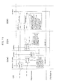
- Fig. 4 is a diagram illustrating a use example of the memory 102 of the information processing apparatus 1 as one example of the first embodiment.
- the memory 102 includes a receiving buffer area 25 (25-0 to 25-15) installed for each BB 100 and an OS area 1023 installed for each OS and further, includes an area 1024 storing priority information 1021.
- the receiving buffer area is called a buffer area or simply called a buffer.
- the OS area 1023 is an area storing data used by the OS.
- a plurality of OS areas 1023 corresponding to the OSs (OSs #0 to #3 in the example illustrated in Fig. 4 ), respectively, are provided as illustrated in Fig. 4 . That is, the OS area 1023 is provided for each OS executed by the BB 100.
- a copy of data which is read out from the buffer area 25 is stored in the OS area 1023 by a data storage processing unit 21 to be described below.
- the OS reads out data from the OS area 1023 used by the OS itself among the plurality of OS areas 1023 and uses the read-out data.
- the buffer area 25 is an area storing data transferred to the CPU 101 and data transferred from another CPU 101 is stored in the buffer area 25.
- a storage area of a part of the memory 102 (priority memory 102) connected to the same MAC 103 as a CPU 101 of a transmission destination of data serves as the buffer area 25.
- a CPU 101 at a side that transmits data is called a transmission source CPU 101 and a CPU 101 at a side that receives data is called a transmission destination CPU 101.
- the buffer area 25 is provided to correspond to each BB 100 provided in the information processing apparatus 1.
- the buffer area 25-0 is provided to correspond to the BB #0 and the buffer area 25-1 is provided to correspond to the BB #1.
- the buffer areas 25-2 to 25-15 are provided to correspond to the BBs #2 to #15, respectively. Note that, as reference numerals representing the buffer areas, when one of the plurality of buffer areas needs to be specified, reference numerals 25-0 to 25-15 are used, but the reference numeral 25 is used at the time of indicating any buffer area.
- the buffer area 25 is provided for each BB 100.
- Fig. 5 is a diagram exemplifying a data configuration written in the buffer area 25 of the information processing apparatus 1 as one example of the first embodiment.
- First data 251a and second data 251b are stored in each buffer area 25, as illustrated in Fig. 5 .
- the first data 251a includes an assignable area (reserved area) apart from a status 2510 indicating a status of the buffer area 25.
- As the status 2510 information indicating any one of "free", "ready", and "busy” is stored.
- free indicates a status in which the buffer area 25 is not locked and indicates a status capable of acquiring an authority to lock and use the buffer area 25 in order to write data in the buffer area 25.
- ready indicates a status (lock status) in which the authority to write data in the buffer area 25 is completely acquired and indicates a status in which data is able to start being written in the buffer area 25.
- busy indicates that data is being written in the buffer area 25.
- Information of the status 2510 is updated by, for example, a data transmission processing unit 12 to be described below.
- the second data 251b includes data 252, data_ready 2520, and a separately assignable area (reserved area).
- the data 252 is data transferred from another CPU 101.
- the data_ready 2520 indicates a status of the data 252 and for example, stores information indicating any one of "false” and "true".
- the transmission destination CPU 101 accesses the data_ready 2520 in order to open the buffer area 25. Note that, the data_ready 2520 is known and is not described in detail.
- the status 2510 which is information accessed by the transmission source CPU 101, is stored in the first data 251a, in transferring data among the CPUs 101.
- the data 252 and the data_ready 2520 which are information accessed by the transmission destination CPU 101, are stored in the second data 251b, in transferring data among the CPUs 101.
- each of the first data 251a and the second data 251b is configured to be the same size as a cache line size of the CPU 101. That is, the first data 251a and the second data 251b are placed to become each line on a cache. As a result, in transferring data among the CPUs 101, access by the transmission source CPU 101 to the status 2510 and access by the transmission destination CPU 101 to the data 252 or the data_ready 2520 are independently performed.
- the transmission source CPU 101 takes lock in order to write data in the buffer area 25 and changes the status 2510 from “free” to “busy”. Further, when storing data in the buffer area 25 is completed, the transmission source CPU 101 changes the status 2510 from "busy” to "ready”. Further, the transmission source CPU 101 changes the data_ready 2520 from "false” to "true” and applies an interrupt to the transmission destination CPU 101 (xcall). The transmission destination CPU 101 verifies that the data_ready 2520 is set as "true” as a free interrupt measure.
- the transmission destination CPU 101 changes the status 2510 from "busy" to "free” and opens the buffer area 25.
- the transmission source CPU 101 changes the status 2510 from "busy" to "free” and opens the buffer area 25.
- simultaneous access by the transmission source CPU 101 and the transmission destination CPU 101 to the same cache line is prevented.
- occurrence of lock competition for accessing the buffer area 25 may be suppressed between the transmission source CPU 101 and the transmission destination CPU 101. That is, false sharing by the transmission source CPU 101 and the transmission destination CPU 101 may be avoided and processing delay caused by the lock competition by the transmission source CPU 101 and the transmission destination CPU 101 may be relieved.
- the data 252 and the data_ready 2520 are provided in the second data 251b, and as a result, the data 252 and the data_ready 2520 are placed on the same line on the cache and the transmission destination CPU 101 may obtain the data 252 and the data_ready 2520 through one access. Therefore, an access frequency to the buffer area 25 may be reduced.
- the priority information 1021 is information indicating the order of priority of each BB 100 provided in the information processing apparatus 1.
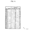
- Fig. 6 is a diagram exemplifying the priority information 1021 in the information processing apparatus 1 as one example of the first embodiment.
- unique priority not to be duplicated with each other is, in advance, set for each BB 100, as exemplified in Fig. 6 .
- two (two types of) priorities are set in each BB 100.
- integers 0 to 15 are set for the BBs #0 to #15 as first priority, respectively and integers 31 to 16 are set for the BBs #0 to #15 as second priority, respectively. Further, it is assumed that in the priorities 0 to 31 exemplified in Fig. 6 , as a numeral value of the priority is larger, the order of priority is higher.
- the priorities 0 to 15 are referred to as low-side priorities (first priority information) and the priorities 16 to 31 are referred to high-side priorities (second priority information).
- the high-side priorities 16 to 31 are higher than any priority of the low-side priorities 0 to 15.
- two priorities of the priority 0 indicating the lowest priority and the priority 31 indicating the highest priority are set in the BB #0 as a pair and two priorities of the low-side priority 3 and the high-side priority 28 are set in the BB #3 as a pair.
- Any one of the two priorities set for the respective BBs 100 is randomly selected by a processing priority setting unit 13 to be described below.
- the priority selected by the processing priority setting unit 13 may be called an interrupt level.
- the priorities set in the respective BBs 100 are set as unique values not to be duplicated for the respective BBs 100.
- the BBs 100 may be specified from the priorities. That is, the priorities are used as node identification information specifying nodes.
- the buffer areas 25 are provided in the priority memory 102 to correspond to the BBs 100, respectively. As a result, the priority serves as identification information indirectly specifying the buffer (storage area) 25.
- the interrupt priority order queue 24 includes a plurality of queues which corresponds to the aforementioned respective priorities of the priority information 1021.
- the interrupt priority order queue 24 corresponds to the priorities 0 to 31 of the priority information 1021 illustrated in Fig. 6 and includes 32 queues.
- any one numerical value of 0 to 31 corresponding to the priorities 0 to 31 is denoted to each queue of the interrupt priority order queue 24.
- Each queue of the interrupt priority order queue 24 corresponds to the interrupt level.
- a flag (for example, "1") is set in each queue of the interrupt priority order queue 24 by the processing priority setting unit 13 to be described below.
- the priority order is set in each queue of the interrupt priority order queue 24 and in the embodiment, queues set with large numerical values among the queues set with the flags by the processing priority setting unit 13 are preferentially processed by an interrupt processing unit 23 to be described below.
- the CPU 101 is a computing device that performs various controls or computations and implements various functions by executing the OS or a control program (hypervisor, HV) stored in the memory 102.
- the hypervisor is a control program for implementing a virtual machine which is one of virtualization technologies of a computer and manages an OS (virtual OS) throughout the plurality of BBs 100.
- each CPU 101 serves as the transmission source CPU 101 that transmits data to other CPUs 101 and serves even as the transmission destination CPU 101 that transmits data transmitted from other CPUs 101.
- the CPU 101 serves as the transmission source CPU 101
- the CPU 101 serves as a cross call reception processing unit 11, the data transmission processing unit 12, the processing priority setting unit 13, and an interrupt generating unit 14, as illustrated in Fig. 1 .
- the CPU 101 serves as the transmission destination CPU 101
- the CPU 101 serves as the interrupt processing unit 23, a data reception processing unit 22, and the data storage processing unit 21, as illustrated in Fig. 1 .
- the CPU 101 executes the hypervisor extended on the memory 102 as the control program to serve as the cross call reception processing unit 11, the data transmission processing unit 12, the processing priority setting unit 13, the interrupt generating unit 14, the interrupt processing unit 23, the data reception processing unit 22, and the data storage processing unit 21. That is, in the information processing apparatus 1 of the first embodiment, the cross call reception processing unit 11, the data transmission processing unit 12, the processing priority setting unit 13, the interrupt generating unit 14, the interrupt processing unit 23, the data reception processing unit 22, and the data storage processing unit 21 are implemented as the function of the hypervisor.
- control program for implementing the functions as the cross call reception processing unit 11, the data transmission processing unit 12, the processing priority setting unit 13, the interrupt generating unit 14, the interrupt processing unit 23, the data reception processing unit 22, and the data storage processing unit 21 is provided while the program is recorded in computer-readable recording media such as, for example, a flexible disk, CDs (a CD-ROM, a CD-R, a CD-RW, and the like), DVDs (a DVD-ROM, a DVD-RAM, a DVD-R, a DVD+R, a DVD-RW, a DVD+RW, an HD DVD, and the like), a Blu-ray disk, a magnetic disk, an optical disk, an optic-magnetic disk, and the like.
- computer-readable recording media such as, for example, a flexible disk, CDs (a CD-ROM, a CD-R, a CD-RW, and the like), DVDs (a DVD-ROM, a DVD-RAM, a DVD-R, a DVD+R, a DVD-RW, a
- the computer reads the program from the recording media and thus transmits the read program to an internal memory device or an external memory device, which is stored and used.
- the program may be recorded in the memory devices (recording media) such as, for example, the magnetic disk, the optical disk, the optic-magnetic disk, and the like and may be provided to the computer from the memory devices through communication routes.
- a program stored in an internal storage device (the memory 102 in the embodiment) is executed by a microprocessor (the CPU 101 in the embodiment) of the computer.
- the computer may read the program recorded in the recording medium to execute the read program.
- the computer is a concept that includes hardware and an operating system and represents hardware that operates under the control of the operating system. Further, when the operating system is unnecessary, and thus an application program singly operates the hardware, the hardware itself corresponds to the computer.
- the hardware at least includes the microprocessor such as the CPU, or the like and method for reading the computer program recorded in the recording medium and in the embodiment, the information processing apparatus 1 or the BB 100 has a function as the computer.
- the cross call reception processing unit 11 receives a cross call transmission request from the OS.
- the data transmission processing unit 12 transmits data to be transferred to the transmission destination CPU 101.
- the data transmission processing unit 12 writes data in the buffer area 25 corresponding to the BB 100 provided in the transmission source CPU 101 in the priority memory 102 corresponding to the transmission destination CPU 101.
- the data transmission processing unit 12 updates the status 2510 of the buffer area 25, or the like. For example, the data transmission processing unit 12 first obtains lock of the target buffer area 25 to change the status 2510 of the buffer area 25 from “free” to "busy” when writing data in the buffer area 25. In addition, the data transmission processing unit 12 changes the data_ready 2520 from “false” to "true” when completes writing data in the buffer area 25.
- the processing priority setting unit 13 determines the transmission destination CPU 101 based on the cross call transmission request which the cross call reception processing unit 11 receives from the OS. Note that, the determination of the transmission destination CPU 101 may be implemented by a known method and will not be described in detail. In addition, the processing priority setting unit 13 randomly selects one priority from a plurality of (two in the embodiment) priorities which is previously assigned to the own BB 100, by referring to, for example, the priority information 1021. That is, the processing priority setting unit 13 sets the interrupt level.
- the interrupt generating unit 14 notifies the interrupt to the transmission destination CPU 101 when the aforementioned data transmission processing unit 12 transmits (stores) data to (in) the buffer area 25 associated with the transmission destination CPU 101 and updates the status 2510 of the buffer area 25, or the like.
- the interrupt generating unit 14 performs the interrupt notification accompanied by the priority selected by the processing priority setting unit 13 to the transmission destination CPU 101.
- the interrupt generating unit 14 sets the flag "1" in a queue corresponding to the priority selected by the processing priority setting unit 13 among the queues of the interrupt priority order queue 24 of the priority memory 102 corresponding to the transmission destination CPU 101, for example.
- the interrupt processing unit 23 specifies from which BB 100 an interrupt processing request is input. In detail, the interrupt processing unit 23 judges which interrupt level (priority) the queue with the set flag in the interrupt priority order queue 24 corresponds to.
- the interrupt processing unit 23 specifies the priority corresponding to the queue with the set flag and further, specifies the BB 100 corresponding to the specified priority.
- the interrupt processing unit 23 notifies the buffer area 25 corresponding to the specified BB 100 to the data reception processing unit 22.
- the data reception processing unit 22 refers to the buffer area 25 notified by the interrupt processing unit 23 and verifies that writing data is completed in the data 252. In detail, the data reception processing unit 22 verifies whether "ready" is set in the status 2510 of the target buffer area 25 and when "ready" is set, the data reception processing unit 22 judges that writing data is completed.
- the data reception processing unit 22 verifies that writing data in the buffer area 25 is completed by the data transmission processing unit 12, the data reception processing unit 22 reads out data from the data 252 of the specified buffer area 25. Further, the data storage processing unit 21 stores a copy of the data read out from the buffer area 25 in the OS area 1023 corresponding to the OS executed by the transmission destination CPU 101. Thereafter, the data storage processing unit 21 accesses the data_ready 2520 of the buffer area 25 to be processed and releases the buffer area 25. Note that, the data copied to the OS area 1023 is processed by the OS.
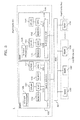
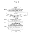
- Fig. 7 is a diagram illustrating a flow of cross call processing in the information processing apparatus 1 as one example of the embodiment.
- a CPU (#0A) which is the transmission source CPU 101
- a CPU (#2A) which is the transmission destination CPU 101
- a right side in the figure is illustrated.
- the cross call reception processing unit 11 receives the cross call from the OS (step A1; see reference numeral F1 of Fig. 7 ).
- the data transmission processing unit 12 verifies whether the buffer area 25 corresponding to the BB 100 of the transmission source CPU 101 is free in the priority memory 102 corresponding to the transmission destination CPU 101.
- the data transmission processing unit 12 verifies whether "free" is stored in the status 2510 and when the status 2510 is not "free” (see route No of step A2), step A2 is repeatedly performed.
- step A2 When the status 2510 is "free” (see route YES of step A2), the data transmission processing unit 12 acquires the lock of the buffer area 25 (see reference numeral F2 of Fig. 7 ) to change the status 2510 of the buffer area 25 from “free” to "busy” (step A3; see reference numeral F3 of Fig. 7 ). Further, in step A4, the data transmission processing unit 12 writes the data 252 in the buffer area 25 of the transmission destination CPU 101 to update the data 252 (see reference numeral F4 of Fig. 7 ). When storing data in the buffer area 25 is completed, in step A5, the data transmission processing unit 12 changes the status 2510 of the buffer area 25 from "busy” to "ready” (see reference numeral F5 of Fig. 7 ) to change the status of the buffer area 25 (see reference numeral F6 of Fig. 7 ).
- the processing priority setting unit 13 randomly selects one priority from a plurality of (two in the embodiment) priorities previously assigned to the own BB 100 and sets the level of the interrupt (see reference numeral F7 of Fig. 7 ).
- two types of high and low priorities are prepared for each BB 100 and the processing priority setting unit 13 randomly selects one priority of two types of priorities to evenly process data transmitted from the plurality of BBs 100 without preferentially executing processing of a specific transmission source CPU 101.
- the processing priority setting unit 13 performs the interrupt notification accompanied by the selected priority to the transmission destination CPU 101 (step A6). As a result, the interrupt is notified to the transmission destination CPU 101 by hardware (see reference numeral F8 of Fig. 7 ).
- the processing priority setting unit 13 sets a flag in a queue corresponding to the selected priority among the queues of the interrupt priority order queue 24 of the priority memory 102 corresponding to the transmission destination CPU 101, and the processing ends.
- step B1 when the transmission destination CPU 101 receives the interrupt from the transmission source CPU 101 (see reference numeral F9 of Fig. 7 ), the interrupt processing unit 23 specifies from which BB 100 an interrupt processing request is input by referring to the interrupt priority order queue 24, in the transmission destination CPU 101. That is, the interrupt processing unit 23 specifies the priority corresponding to the queue with the set flag and further, specifies the BB 100 corresponding to the specified priority.
- step B2 the data reception processing unit 22 verifies that writing data is completed by referring to the buffer area 25 notified by the interrupt processing unit 23 (see reference numeral F10 of Fig. 7 ). In detail, the data reception processing unit 22 verifies whether "ready” is stored in the status 2510 and when the status 2510 is not "ready” (see route No of step B2), step B2 is repeatedly performed.
- the transmission destination CPU 101 it may be specified which BB 100 data is stored in the buffer area 25 corresponding to by the priority of the interrupt priority order queue 24.
- the data reception processing unit 22 checks only the status 2510 of the buffer area 25 corresponding to the target BB 100, and may verify the status 2510 within a short time and rapidly perform read-out processing by the transmission destination CPU 101.
- step B2 When the status 2510 is "ready” (see route YES of step B2), the data storage processing unit 21 stores the copy of the data read out from the buffer area 25 in the OS area 1023, in step B3. Thereafter, the data storage processing unit 21 changes the status 2510 of the buffer area 25 from “ready” to “free” and releases the buffer area 25, in step B4 (see reference numeral F12 of Fig. 7 ). Thereafter, in step B5, receiving the cross call is completed (see reference numeral F13 of Fig. 7 ) and the processing ends.
- Fig. 10 is a diagram describing a method for transferring data among the CPUs 101 in the information processing apparatus 1 as one example of the first embodiment.
- the priorities 0 and 31 are set in the BB #0 and the priorities 1 and 30 are set in the BB #1.
- each of CPUs #0A, #0B, and #0C intends to transfer data to a CPU #2A of a BB #2 and among them, the CPU #0A obtains lock of the buffer area 25-0 for the BB #0 provided in the BB #2.
- the CPU #0A randomly selects any one priority from the priorities "0" and "31" which are previously set in the BB #0 and performs interrupt notification accompanied by the selected priority to the CPU #2A. Note that, until each of the CPUs #0B and #0C which do not obtain the lock is able to take the lock of the buffer area 25-0, the CPUs #0B and #0C repeatedly access the status 2510.
- the CPU #2A includes the buffer area 25 for each BB 100.
- the CPU #1A of the BB #1 may obtain lock of the buffer area 25-1 for the BB #1 provided in the BB #2. That is, the CPU #1A of the BB #1 does not compete with the CPUs #0B and #0C of the BB #0 and may take the lock of the buffer area 25-1.
- the CPU #1A randomly selects any one priority from the priorities "1" and "30" which are previously set in the BB #1 and performs interrupt notification accompanied by the selected priority to the CPU #2A.
- the CPU (#1A) may know which buffer area 25 BB 100 corresponds to is updated, by referring to the notified priority.
- the CPU #2A processes data of the buffer area 25-0 corresponding to the BB #0 when the priority notified by the interrupt notification of the cross call is "0" or "31". Similarly, the CPU #2A processes data of the buffer area 25-1 corresponding to the BB #1 when the priority notified by the interrupt notification of the cross call is "1" or "30".
- the CPU #2A verifies only the status 2510 of the buffer area 25 corresponding to the notified priority and may read out the data from the buffer area 25 in a short time and rapidly process the cross call.
- the transmission destination CPU 101 may specify which BB 100 the interrupt is from by referring to the priority notified by the interrupt notification of the cross call. As a result, the CPU 101 may read out the data from the buffer area 25 within a short time and rapidly process the cross call.
- cross call access competition by the transmission source CPUs 101 of the respective BBs 100 to the buffer area 25 of the transmission destination CPU 101 may be avoided.
- processing delay of CPU communication by access competition among the CPUs 101 may be resolved and rapid interCPU communications in a large configuration may be implemented.
- occurrence of a cross call time-out may be suppressed and the reliability of the apparatus may be improved.
- a plurality of priorities are provided for each BB 100, and the processing priority setting unit 13 notifies the priority randomly selected from the priorities to the transmission destination CPU 101 by the interrupt notification of the cross call.
- continuously processing some BBs 100 preferably may be avoided and occurrence of a situation in which processing from a specific BB 100 continuously takes a time may be suppressed.
- the first data 251a and the second data 251b are placed to become each line on a cache.
- the first data 251a includes the status 2510 and the second data 251b includes the data 252 and the data_ready 2520.
- the data 252 and the data_ready 2520 are provided in the second data 251b, and as a result, the data 252 and the data_ready 2520 are placed on the same line on the cache and the transmission destination CPU 101 may obtain the data 252 and the data_ready 2520 through one access. Therefore, an access frequency to the buffer area 25 may be reduced.
- the buffer area 25 is provided for each BB 100 in the priority memory 102 of the transmission destination CPU 101 and the invention is not limited thereto.
- the buffer area 25 is provided in each priority memory 102 of the transmission source CPU 101 and the transmission source CPU 101 stores data transferred to the transmission destination CPU 101 in the buffer area 25 managed by the transmission source CPU 101.
- the other parts are configured similarly to the information processing apparatus 1 of the first embodiment. That is, in the first embodiment, the buffer area is present in the transmission destination, while in the second embodiment, an example in which the buffer area is present in the transmission source will be described below.
- Fig. 11 is a diagram describing a method for transferring data among the CPUs 101 in the information processing apparatus 1 as one example of the second embodiment.
- different priority information 1021 is set for each CPU 101, instead of the BB 100 of the first embodiment. Further, even in the second embodiment, two types of priorities (first priority information and second priority information) are set as the priority information, similarly to the first embodiment.
- the priorities set for each CPU 101 are set as unique values which are not duplicated with each other with respect to each CPU 101. As a result, the transmission source CPU 101 may be specified from the priorities.
- the buffer area 25 is provided for each CPU 101 in the BB 100.
- the priority serves as identification information to specify the buffer (storage area) 25.
- each of the CPUs #0A, #0B, and #0C intends to transfer data to the CPU #2A of the BB #2.
- the CPU #0A obtains lock of a buffer area 25-0A of the its own priority memory 102 and stores data in the buffer area 25-0A.
- the CPU #0A may obtain the lock of the buffer area 25-0A without competing with other CPUs 101 (for example, the CPUs #0B and #0C).
- the CPU #0A randomly selects any one priority from the priorities "0" and "31" which are previously set in the BB #0 and performs interrupt notification accompanied by the selected priority X to the CPU #2A.
- the CPU #0B obtains lock of a buffer area 25-0B of its own priority memory 102, stores data in the buffer area 25-0B, and further, the CPU #0C obtains lock of a buffer area 25-0C of its own priority memory 102 and stores data in the buffer area 25-0C. Even the CPUs #0A to #0C may obtain the lock of the buffer areas 25-0B and 25-0C without competing with other CPUs 101.
- the CPU #1A obtains the lock of the buffer area 25-1A of its own priority memory 102 and stores data in the buffer area 25-1A.
- the CPU #1A may obtain the lock of the buffer area 25-0A without competing with other CPUs 101 (for example, the CPUs #0B and #0C).
- the CPU #1A randomly selects any one priority from the priorities "1" and "30" which are previously set in the BB #1 and performs interrupt notification accompanied by the selected priority Y to the CPU #2A.
- each CPU 101 may obtain the lock of the buffer area 25 without competing with other CPUs 101 as well as the same operational effect as the first embodiment may be acquired. That is, in each CPU 101, since competition for obtaining the lock for writing data in the buffer area 25 does not occur and delay of processing by the lock competition does not occur, the processing may be rapidly performed.
- each configuration and each processing of the embodiments may be selected as necessary or may be appropriately combined.
- unique priority is set for each node 100 or each CPU 101 and the transmission source node 100 or CPU 101 is specified based on the priority, but the invention is not limited thereto.
- unique identification information may be set for individual nodes 100 or CPUs 101, respectively, and the transmission source CPU 101 may notify the identification information to the transmission destination CPU 101 to specify the transmission source node 100 or CPU 101 in the transmission destination CPU 101.
- the buffer area 25 is provided for each CPU 101 in the transmission source BB 100, but the invention is not limited thereto. That is, in the transmission source BB 100, the plurality of CPUs 101 may include a common buffer area 25. As a result, in the transmission source BB 100, the size of the buffer area 25 may be decreased.
- different priority information 1021 is set for each CPU 101, but the invention is not limited thereto and similarly to the first embodiment, different priority information 1021 may be set for each BB 100.
- the embodiment may be worked and manufactured by those skilled in the art by the aforementioned disclosure.
Landscapes
- Engineering & Computer Science (AREA)
- Theoretical Computer Science (AREA)
- Software Systems (AREA)
- Physics & Mathematics (AREA)
- General Engineering & Computer Science (AREA)
- General Physics & Mathematics (AREA)
- Multi Processors (AREA)
- Bus Control (AREA)
Applications Claiming Priority (1)
| Application Number | Priority Date | Filing Date | Title |
|---|---|---|---|
| JP2012192392A JP6079065B2 (ja) | 2012-08-31 | 2012-08-31 | 情報処理装置,処理方法及びプログラム |
Publications (3)
| Publication Number | Publication Date |
|---|---|
| EP2704009A2 true EP2704009A2 (fr) | 2014-03-05 |
| EP2704009A3 EP2704009A3 (fr) | 2015-01-14 |
| EP2704009B1 EP2704009B1 (fr) | 2019-04-24 |
Family
ID=48747982
Family Applications (1)
| Application Number | Title | Priority Date | Filing Date |
|---|---|---|---|
| EP13175508.4A Active EP2704009B1 (fr) | 2012-08-31 | 2013-07-08 | Appareil de traitement d' informations, procédé et programme de traitement d' informations |
Country Status (3)
| Country | Link |
|---|---|
| US (1) | US9063929B2 (fr) |
| EP (1) | EP2704009B1 (fr) |
| JP (1) | JP6079065B2 (fr) |
Cited By (1)
| Publication number | Priority date | Publication date | Assignee | Title |
|---|---|---|---|---|
| CN104268111A (zh) * | 2014-09-17 | 2015-01-07 | 海信(山东)冰箱有限公司 | 一种数据处理的方法及装置 |
Families Citing this family (6)
| Publication number | Priority date | Publication date | Assignee | Title |
|---|---|---|---|---|
| EP3125056B1 (fr) * | 2015-07-30 | 2021-04-07 | Siemens Aktiengesellschaft | Systeme et procede de commande et/ou d'analyse d'un processus industriel |
| JP6859642B2 (ja) * | 2016-09-23 | 2021-04-14 | カシオ計算機株式会社 | 制御装置、電子時計、処理制御方法、及びプログラム |
| US20220217764A1 (en) * | 2019-04-30 | 2022-07-07 | Ntt Docomo, Inc. | User equipment and communication method |
| CN112286657A (zh) * | 2020-10-23 | 2021-01-29 | 海光信息技术股份有限公司 | 电子设备和中断处理方法 |
| CN118414604A (zh) * | 2021-12-30 | 2024-07-30 | 华为技术有限公司 | 计算装置中的跨域通信方法和跨域通信装置 |
| CN114477883B (zh) * | 2022-02-10 | 2022-09-13 | 青岛光大集团大型构件有限公司 | 一种高强隔音混凝土及其制备方法及混凝土预制叠合板 |
Citations (5)
| Publication number | Priority date | Publication date | Assignee | Title |
|---|---|---|---|---|
| JPS6359649A (ja) | 1986-08-29 | 1988-03-15 | Fujitsu Ltd | プロセツサ間の通信方式 |
| JPH11120156A (ja) | 1997-10-17 | 1999-04-30 | Nec Corp | マルチプロセッサシステムにおけるデータ通信方式 |
| JP2000029850A (ja) | 1998-07-09 | 2000-01-28 | Nec Data Terminal Ltd | オペレーティングシステムのプロセッサ間通信を使用したタスク制御方法 |
| JP2004086615A (ja) | 2002-08-27 | 2004-03-18 | Matsushita Electric Ind Co Ltd | バス通信装置 |
| JP2006301894A (ja) | 2005-04-20 | 2006-11-02 | Nec Electronics Corp | マルチプロセッサシステム、及びマルチプロセッサシステムのメッセージ伝達方法 |
Family Cites Families (27)
| Publication number | Priority date | Publication date | Assignee | Title |
|---|---|---|---|---|
| JP2872259B2 (ja) * | 1989-03-17 | 1999-03-17 | 株式会社日立製作所 | マルチプロセッサシステム |
| JPH05143364A (ja) | 1991-11-22 | 1993-06-11 | Fujitsu Ltd | 割込制御装置 |
| JP3312362B2 (ja) * | 1994-08-26 | 2002-08-05 | 日本電信電話株式会社 | マルチプロセッサシステム |
| JPH07200494A (ja) | 1993-12-28 | 1995-08-04 | Mitsubishi Electric Corp | 分散制御方式 |
| JP3312361B2 (ja) * | 1994-04-13 | 2002-08-05 | 日本電信電話株式会社 | 分散共有メモリシステム |
| JP2940403B2 (ja) * | 1994-08-03 | 1999-08-25 | 株式会社日立製作所 | 並列計算機システムにおけるモニタデータ収集方法 |
| JPH09162873A (ja) * | 1995-12-05 | 1997-06-20 | Nippon Telegr & Teleph Corp <Ntt> | 誤り検出方法および装置 |
| JP3576437B2 (ja) * | 1999-11-30 | 2004-10-13 | 松下電器産業株式会社 | マルチプロセッサタスク制御方法及びタスク制御装置 |
| US7379994B2 (en) * | 2000-10-26 | 2008-05-27 | Metilinx | Aggregate system resource analysis including correlation matrix and metric-based analysis |
| US6813665B2 (en) * | 2001-09-21 | 2004-11-02 | Intel Corporation | Interrupt method, system and medium |
| JP3640187B2 (ja) * | 2002-07-29 | 2005-04-20 | 日本電気株式会社 | マルチプロセッサシステムの障害処理方法、マルチプロセッサシステム及びノード |
| US7222262B2 (en) * | 2003-08-05 | 2007-05-22 | Newisys, Inc. | Methods and devices for injecting commands in systems having multiple multi-processor clusters |
| US7194598B2 (en) * | 2004-01-26 | 2007-03-20 | Nvidia Corporation | System and method using embedded microprocessor as a node in an adaptable computing machine |
| JP4298543B2 (ja) * | 2004-02-24 | 2009-07-22 | 京セラミタ株式会社 | 割り込み制御装置 |
| JP2006119802A (ja) * | 2004-10-20 | 2006-05-11 | Hitachi Ltd | マルチプロセッサシステム |
| EP1669864B1 (fr) * | 2004-12-03 | 2010-06-02 | STMicroelectronics Srl | Un processus pour gérer des machines virtuelles dans une machine de traitement physique, système de processeur correspondant et produit logiciel pour ce but |
| JP4856413B2 (ja) * | 2005-10-04 | 2012-01-18 | 富士通株式会社 | 演算処理装置、情報処理装置、及び演算処理装置の制御方法 |
| US20080162762A1 (en) * | 2006-12-29 | 2008-07-03 | Gilbert Neiger | Interrupt remapping based on requestor identification |
| US7849247B2 (en) * | 2008-10-14 | 2010-12-07 | Freescale Semiconductor, Inc. | Interrupt controller for accelerated interrupt handling in a data processing system and method thereof |
| JP5217929B2 (ja) * | 2008-11-13 | 2013-06-19 | ソニー株式会社 | 割込検出装置および情報処理システム |
| US8028017B2 (en) * | 2009-04-16 | 2011-09-27 | International Business Machines Corporation | Virtual controllers with a large data center |
| JP4854050B2 (ja) * | 2009-09-24 | 2012-01-11 | エヌイーシーコンピュータテクノ株式会社 | ノード制御装置、ノード制御装置の制御方法、情報処理システム、及びコンピュータプログラム |
| WO2011111172A1 (fr) * | 2010-03-09 | 2011-09-15 | 富士通株式会社 | Dispositif de traitement d'informations, procédé et programme de traitement d'informations |
| JPWO2011114476A1 (ja) * | 2010-03-17 | 2013-06-27 | 富士通株式会社 | マルチコアプロセッサシステム、通知プログラム、および通知方法 |
| KR101717494B1 (ko) * | 2010-10-08 | 2017-03-28 | 삼성전자주식회사 | 인터럽트 처리 장치 및 방법 |
| US8812916B2 (en) * | 2011-06-02 | 2014-08-19 | International Business Machines Corporation | Failure data management for a distributed computer system |
| US9678801B2 (en) * | 2012-08-09 | 2017-06-13 | International Business Machines Corporation | Service management modes of operation in distributed node service management |
-
2012
- 2012-08-31 JP JP2012192392A patent/JP6079065B2/ja active Active
-
2013
- 2013-07-08 EP EP13175508.4A patent/EP2704009B1/fr active Active
- 2013-07-08 US US13/936,532 patent/US9063929B2/en active Active
Patent Citations (5)
| Publication number | Priority date | Publication date | Assignee | Title |
|---|---|---|---|---|
| JPS6359649A (ja) | 1986-08-29 | 1988-03-15 | Fujitsu Ltd | プロセツサ間の通信方式 |
| JPH11120156A (ja) | 1997-10-17 | 1999-04-30 | Nec Corp | マルチプロセッサシステムにおけるデータ通信方式 |
| JP2000029850A (ja) | 1998-07-09 | 2000-01-28 | Nec Data Terminal Ltd | オペレーティングシステムのプロセッサ間通信を使用したタスク制御方法 |
| JP2004086615A (ja) | 2002-08-27 | 2004-03-18 | Matsushita Electric Ind Co Ltd | バス通信装置 |
| JP2006301894A (ja) | 2005-04-20 | 2006-11-02 | Nec Electronics Corp | マルチプロセッサシステム、及びマルチプロセッサシステムのメッセージ伝達方法 |
Cited By (2)
| Publication number | Priority date | Publication date | Assignee | Title |
|---|---|---|---|---|
| CN104268111A (zh) * | 2014-09-17 | 2015-01-07 | 海信(山东)冰箱有限公司 | 一种数据处理的方法及装置 |
| CN104268111B (zh) * | 2014-09-17 | 2017-12-01 | 海信(山东)冰箱有限公司 | 一种数据处理的方法及装置 |
Also Published As
| Publication number | Publication date |
|---|---|
| US20140068115A1 (en) | 2014-03-06 |
| JP2014048965A (ja) | 2014-03-17 |
| EP2704009A3 (fr) | 2015-01-14 |
| US9063929B2 (en) | 2015-06-23 |
| JP6079065B2 (ja) | 2017-02-15 |
| EP2704009B1 (fr) | 2019-04-24 |
Similar Documents
| Publication | Publication Date | Title |
|---|---|---|
| EP2704009A2 (fr) | Appareil de traitement d' informations, procédé et programme de traitement d'informations | |
| US11128555B2 (en) | Methods and apparatus for SDI support for automatic and transparent migration | |
| US10572290B2 (en) | Method and apparatus for allocating a physical resource to a virtual machine | |
| JP5315209B2 (ja) | 冗長構成を生成するための周辺機器相互接続入出力仮想化デバイスの使用 | |
| US9807028B2 (en) | Method and apparatus for allocating resources | |
| US8301806B2 (en) | Configuring an input/output adapter | |
| CN109688058B (zh) | 报文处理方法、装置及网络设备 | |
| WO2018036103A1 (fr) | Procédé et système de création d'une machine virtuelle et ordinateur hôte | |
| US8447891B2 (en) | Dynamically assigning virtual functions to client applications | |
| US8225005B2 (en) | Use of peripheral component interconnect input/output virtualization devices to create high-speed, low-latency interconnect | |
| US8527666B2 (en) | Accessing a configuration space of a virtual function | |
| WO2019056771A1 (fr) | Procédé et dispositif de gestion de mise à niveau de système de mémoire partagée, et système de mémoire partagée | |
| US11055104B2 (en) | Network-adapter configuration using option-ROM in multi-CPU devices | |
| US20100100776A1 (en) | Information processing apparatus, failure processing method, and recording medium in which failure processing program is recorded | |
| CN104731635A (zh) | 一种虚拟机访问控制方法,及虚拟机访问控制系统 | |
| CN114691037A (zh) | 卸载卡命名空间管理、输入输出请求处理系统和方法 | |
| KR101821016B1 (ko) | 제어 시스템의 구성요소에 식별자를 할당하는 장치, 시스템 및 방법 | |
| US10216664B2 (en) | Remote resource access method and switching device | |
| CN117009266A (zh) | 一种握手协议总线仲裁模块及片上系统 | |
| WO2016154860A1 (fr) | Procédé, appareil et système d'établissement d'interface entre gestionnaires de fonctions de réseau virtualisé (vfnm) | |
| CN107615872B (zh) | 一种释放连接的方法、装置及系统 | |
| KR20130104958A (ko) | 다중 운영체제들을 실행하는 장치 및 방법 | |
| US8346988B2 (en) | Techniques for dynamically sharing a fabric to facilitate off-chip communication for multiple on-chip units | |
| US10037257B1 (en) | Examining local hardware using a location-aware peripheral device | |
| US20230067658A1 (en) | System and operation method of hybrid virtual machine managers |
Legal Events
| Date | Code | Title | Description |
|---|---|---|---|
| AK | Designated contracting states |
Kind code of ref document: A2 Designated state(s): AL AT BE BG CH CY CZ DE DK EE ES FI FR GB GR HR HU IE IS IT LI LT LU LV MC MK MT NL NO PL PT RO RS SE SI SK SM TR |
|
| AX | Request for extension of the european patent |
Extension state: BA ME |
|
| PUAI | Public reference made under article 153(3) epc to a published international application that has entered the european phase |
Free format text: ORIGINAL CODE: 0009012 |
|
| PUAL | Search report despatched |
Free format text: ORIGINAL CODE: 0009013 |
|
| AK | Designated contracting states |
Kind code of ref document: A3 Designated state(s): AL AT BE BG CH CY CZ DE DK EE ES FI FR GB GR HR HU IE IS IT LI LT LU LV MC MK MT NL NO PL PT RO RS SE SI SK SM TR |
|
| AX | Request for extension of the european patent |
Extension state: BA ME |
|
| RIC1 | Information provided on ipc code assigned before grant |
Ipc: G06F 13/34 20060101ALI20141210BHEP Ipc: G06F 9/48 20060101AFI20141210BHEP Ipc: G06F 13/28 20060101ALI20141210BHEP Ipc: G06F 13/24 20060101ALI20141210BHEP Ipc: G06F 9/54 20060101ALI20141210BHEP |
|
| 17P | Request for examination filed |
Effective date: 20150527 |
|
| RBV | Designated contracting states (corrected) |
Designated state(s): AL AT BE BG CH CY CZ DE DK EE ES FI FR GB GR HR HU IE IS IT LI LT LU LV MC MK MT NL NO PL PT RO RS SE SI SK SM TR |
|
| STAA | Information on the status of an ep patent application or granted ep patent |
Free format text: STATUS: EXAMINATION IS IN PROGRESS |
|
| 17Q | First examination report despatched |
Effective date: 20180504 |
|
| GRAP | Despatch of communication of intention to grant a patent |
Free format text: ORIGINAL CODE: EPIDOSNIGR1 |
|
| STAA | Information on the status of an ep patent application or granted ep patent |
Free format text: STATUS: GRANT OF PATENT IS INTENDED |
|
| INTG | Intention to grant announced |
Effective date: 20190108 |
|
| GRAS | Grant fee paid |
Free format text: ORIGINAL CODE: EPIDOSNIGR3 |
|
| GRAJ | Information related to disapproval of communication of intention to grant by the applicant or resumption of examination proceedings by the epo deleted |
Free format text: ORIGINAL CODE: EPIDOSDIGR1 |
|
| GRAL | Information related to payment of fee for publishing/printing deleted |
Free format text: ORIGINAL CODE: EPIDOSDIGR3 |
|
| STAA | Information on the status of an ep patent application or granted ep patent |
Free format text: STATUS: EXAMINATION IS IN PROGRESS |
|
| GRAR | Information related to intention to grant a patent recorded |
Free format text: ORIGINAL CODE: EPIDOSNIGR71 |
|
| STAA | Information on the status of an ep patent application or granted ep patent |
Free format text: STATUS: GRANT OF PATENT IS INTENDED |
|
| GRAA | (expected) grant |
Free format text: ORIGINAL CODE: 0009210 |
|
| STAA | Information on the status of an ep patent application or granted ep patent |
Free format text: STATUS: THE PATENT HAS BEEN GRANTED |
|
| INTC | Intention to grant announced (deleted) | ||
| AK | Designated contracting states |
Kind code of ref document: B1 Designated state(s): AL AT BE BG CH CY CZ DE DK EE ES FI FR GB GR HR HU IE IS IT LI LT LU LV MC MK MT NL NO PL PT RO RS SE SI SK SM TR |
|
| INTG | Intention to grant announced |
Effective date: 20190315 |
|
| REG | Reference to a national code |
Ref country code: GB Ref legal event code: FG4D |
|
| REG | Reference to a national code |
Ref country code: CH Ref legal event code: EP |
|
| REG | Reference to a national code |
Ref country code: AT Ref legal event code: REF Ref document number: 1124931 Country of ref document: AT Kind code of ref document: T Effective date: 20190515 Ref country code: IE Ref legal event code: FG4D |
|
| REG | Reference to a national code |
Ref country code: DE Ref legal event code: R096 Ref document number: 602013054213 Country of ref document: DE |
|
| REG | Reference to a national code |
Ref country code: NL Ref legal event code: MP Effective date: 20190424 |
|
| REG | Reference to a national code |
Ref country code: LT Ref legal event code: MG4D |
|
| PG25 | Lapsed in a contracting state [announced via postgrant information from national office to epo] |
Ref country code: NL Free format text: LAPSE BECAUSE OF FAILURE TO SUBMIT A TRANSLATION OF THE DESCRIPTION OR TO PAY THE FEE WITHIN THE PRESCRIBED TIME-LIMIT Effective date: 20190424 |
|
| PG25 | Lapsed in a contracting state [announced via postgrant information from national office to epo] |
Ref country code: NO Free format text: LAPSE BECAUSE OF FAILURE TO SUBMIT A TRANSLATION OF THE DESCRIPTION OR TO PAY THE FEE WITHIN THE PRESCRIBED TIME-LIMIT Effective date: 20190724 Ref country code: FI Free format text: LAPSE BECAUSE OF FAILURE TO SUBMIT A TRANSLATION OF THE DESCRIPTION OR TO PAY THE FEE WITHIN THE PRESCRIBED TIME-LIMIT Effective date: 20190424 Ref country code: PT Free format text: LAPSE BECAUSE OF FAILURE TO SUBMIT A TRANSLATION OF THE DESCRIPTION OR TO PAY THE FEE WITHIN THE PRESCRIBED TIME-LIMIT Effective date: 20190824 Ref country code: AL Free format text: LAPSE BECAUSE OF FAILURE TO SUBMIT A TRANSLATION OF THE DESCRIPTION OR TO PAY THE FEE WITHIN THE PRESCRIBED TIME-LIMIT Effective date: 20190424 Ref country code: SE Free format text: LAPSE BECAUSE OF FAILURE TO SUBMIT A TRANSLATION OF THE DESCRIPTION OR TO PAY THE FEE WITHIN THE PRESCRIBED TIME-LIMIT Effective date: 20190424 Ref country code: HR Free format text: LAPSE BECAUSE OF FAILURE TO SUBMIT A TRANSLATION OF THE DESCRIPTION OR TO PAY THE FEE WITHIN THE PRESCRIBED TIME-LIMIT Effective date: 20190424 Ref country code: LT Free format text: LAPSE BECAUSE OF FAILURE TO SUBMIT A TRANSLATION OF THE DESCRIPTION OR TO PAY THE FEE WITHIN THE PRESCRIBED TIME-LIMIT Effective date: 20190424 Ref country code: ES Free format text: LAPSE BECAUSE OF FAILURE TO SUBMIT A TRANSLATION OF THE DESCRIPTION OR TO PAY THE FEE WITHIN THE PRESCRIBED TIME-LIMIT Effective date: 20190424 |
|
| PG25 | Lapsed in a contracting state [announced via postgrant information from national office to epo] |
Ref country code: BG Free format text: LAPSE BECAUSE OF FAILURE TO SUBMIT A TRANSLATION OF THE DESCRIPTION OR TO PAY THE FEE WITHIN THE PRESCRIBED TIME-LIMIT Effective date: 20190724 Ref country code: RS Free format text: LAPSE BECAUSE OF FAILURE TO SUBMIT A TRANSLATION OF THE DESCRIPTION OR TO PAY THE FEE WITHIN THE PRESCRIBED TIME-LIMIT Effective date: 20190424 Ref country code: PL Free format text: LAPSE BECAUSE OF FAILURE TO SUBMIT A TRANSLATION OF THE DESCRIPTION OR TO PAY THE FEE WITHIN THE PRESCRIBED TIME-LIMIT Effective date: 20190424 Ref country code: GR Free format text: LAPSE BECAUSE OF FAILURE TO SUBMIT A TRANSLATION OF THE DESCRIPTION OR TO PAY THE FEE WITHIN THE PRESCRIBED TIME-LIMIT Effective date: 20190725 Ref country code: LV Free format text: LAPSE BECAUSE OF FAILURE TO SUBMIT A TRANSLATION OF THE DESCRIPTION OR TO PAY THE FEE WITHIN THE PRESCRIBED TIME-LIMIT Effective date: 20190424 |
|
| REG | Reference to a national code |
Ref country code: AT Ref legal event code: MK05 Ref document number: 1124931 Country of ref document: AT Kind code of ref document: T Effective date: 20190424 |
|
| PG25 | Lapsed in a contracting state [announced via postgrant information from national office to epo] |
Ref country code: IS Free format text: LAPSE BECAUSE OF FAILURE TO SUBMIT A TRANSLATION OF THE DESCRIPTION OR TO PAY THE FEE WITHIN THE PRESCRIBED TIME-LIMIT Effective date: 20190824 |
|
| REG | Reference to a national code |
Ref country code: DE Ref legal event code: R097 Ref document number: 602013054213 Country of ref document: DE |
|
| PG25 | Lapsed in a contracting state [announced via postgrant information from national office to epo] |
Ref country code: SK Free format text: LAPSE BECAUSE OF FAILURE TO SUBMIT A TRANSLATION OF THE DESCRIPTION OR TO PAY THE FEE WITHIN THE PRESCRIBED TIME-LIMIT Effective date: 20190424 Ref country code: RO Free format text: LAPSE BECAUSE OF FAILURE TO SUBMIT A TRANSLATION OF THE DESCRIPTION OR TO PAY THE FEE WITHIN THE PRESCRIBED TIME-LIMIT Effective date: 20190424 Ref country code: CZ Free format text: LAPSE BECAUSE OF FAILURE TO SUBMIT A TRANSLATION OF THE DESCRIPTION OR TO PAY THE FEE WITHIN THE PRESCRIBED TIME-LIMIT Effective date: 20190424 Ref country code: DK Free format text: LAPSE BECAUSE OF FAILURE TO SUBMIT A TRANSLATION OF THE DESCRIPTION OR TO PAY THE FEE WITHIN THE PRESCRIBED TIME-LIMIT Effective date: 20190424 Ref country code: AT Free format text: LAPSE BECAUSE OF FAILURE TO SUBMIT A TRANSLATION OF THE DESCRIPTION OR TO PAY THE FEE WITHIN THE PRESCRIBED TIME-LIMIT Effective date: 20190424 Ref country code: EE Free format text: LAPSE BECAUSE OF FAILURE TO SUBMIT A TRANSLATION OF THE DESCRIPTION OR TO PAY THE FEE WITHIN THE PRESCRIBED TIME-LIMIT Effective date: 20190424 |
|
| PG25 | Lapsed in a contracting state [announced via postgrant information from national office to epo] |
Ref country code: SM Free format text: LAPSE BECAUSE OF FAILURE TO SUBMIT A TRANSLATION OF THE DESCRIPTION OR TO PAY THE FEE WITHIN THE PRESCRIBED TIME-LIMIT Effective date: 20190424 Ref country code: IT Free format text: LAPSE BECAUSE OF FAILURE TO SUBMIT A TRANSLATION OF THE DESCRIPTION OR TO PAY THE FEE WITHIN THE PRESCRIBED TIME-LIMIT Effective date: 20190424 Ref country code: MC Free format text: LAPSE BECAUSE OF FAILURE TO SUBMIT A TRANSLATION OF THE DESCRIPTION OR TO PAY THE FEE WITHIN THE PRESCRIBED TIME-LIMIT Effective date: 20190424 |
|
| PLBE | No opposition filed within time limit |
Free format text: ORIGINAL CODE: 0009261 |
|
| REG | Reference to a national code |
Ref country code: CH Ref legal event code: PL |
|
| STAA | Information on the status of an ep patent application or granted ep patent |
Free format text: STATUS: NO OPPOSITION FILED WITHIN TIME LIMIT |
|
| PG25 | Lapsed in a contracting state [announced via postgrant information from national office to epo] |
Ref country code: TR Free format text: LAPSE BECAUSE OF FAILURE TO SUBMIT A TRANSLATION OF THE DESCRIPTION OR TO PAY THE FEE WITHIN THE PRESCRIBED TIME-LIMIT Effective date: 20190424 |
|
| 26N | No opposition filed |
Effective date: 20200127 |
|
| REG | Reference to a national code |
Ref country code: BE Ref legal event code: MM Effective date: 20190731 |
|
| PG25 | Lapsed in a contracting state [announced via postgrant information from national office to epo] |
Ref country code: LU Free format text: LAPSE BECAUSE OF NON-PAYMENT OF DUE FEES Effective date: 20190708 Ref country code: BE Free format text: LAPSE BECAUSE OF NON-PAYMENT OF DUE FEES Effective date: 20190731 Ref country code: SI Free format text: LAPSE BECAUSE OF FAILURE TO SUBMIT A TRANSLATION OF THE DESCRIPTION OR TO PAY THE FEE WITHIN THE PRESCRIBED TIME-LIMIT Effective date: 20190424 Ref country code: LI Free format text: LAPSE BECAUSE OF NON-PAYMENT OF DUE FEES Effective date: 20190731 Ref country code: CH Free format text: LAPSE BECAUSE OF NON-PAYMENT OF DUE FEES Effective date: 20190731 |
|
| PG25 | Lapsed in a contracting state [announced via postgrant information from national office to epo] |
Ref country code: IE Free format text: LAPSE BECAUSE OF NON-PAYMENT OF DUE FEES Effective date: 20190708 |
|
| PG25 | Lapsed in a contracting state [announced via postgrant information from national office to epo] |
Ref country code: CY Free format text: LAPSE BECAUSE OF FAILURE TO SUBMIT A TRANSLATION OF THE DESCRIPTION OR TO PAY THE FEE WITHIN THE PRESCRIBED TIME-LIMIT Effective date: 20190424 |
|
| PG25 | Lapsed in a contracting state [announced via postgrant information from national office to epo] |
Ref country code: HU Free format text: LAPSE BECAUSE OF FAILURE TO SUBMIT A TRANSLATION OF THE DESCRIPTION OR TO PAY THE FEE WITHIN THE PRESCRIBED TIME-LIMIT; INVALID AB INITIO Effective date: 20130708 Ref country code: MT Free format text: LAPSE BECAUSE OF FAILURE TO SUBMIT A TRANSLATION OF THE DESCRIPTION OR TO PAY THE FEE WITHIN THE PRESCRIBED TIME-LIMIT Effective date: 20190424 |
|
| PG25 | Lapsed in a contracting state [announced via postgrant information from national office to epo] |
Ref country code: MK Free format text: LAPSE BECAUSE OF FAILURE TO SUBMIT A TRANSLATION OF THE DESCRIPTION OR TO PAY THE FEE WITHIN THE PRESCRIBED TIME-LIMIT Effective date: 20190424 |
|
| PGFP | Annual fee paid to national office [announced via postgrant information from national office to epo] |
Ref country code: DE Payment date: 20230531 Year of fee payment: 11 |
|
| PGFP | Annual fee paid to national office [announced via postgrant information from national office to epo] |
Ref country code: GB Payment date: 20240620 Year of fee payment: 12 |
|
| PGFP | Annual fee paid to national office [announced via postgrant information from national office to epo] |
Ref country code: FR Payment date: 20240619 Year of fee payment: 12 |