EP2689431B1 - Druckempfindliche polymerverbundstoff angepasst für berührungsbildschirm - Google Patents
Druckempfindliche polymerverbundstoff angepasst für berührungsbildschirm Download PDFInfo
- Publication number
- EP2689431B1 EP2689431B1 EP12717435.7A EP12717435A EP2689431B1 EP 2689431 B1 EP2689431 B1 EP 2689431B1 EP 12717435 A EP12717435 A EP 12717435A EP 2689431 B1 EP2689431 B1 EP 2689431B1
- Authority
- EP
- European Patent Office
- Prior art keywords
- conductive
- composite material
- layer
- agglomerates
- carrier layer
- Prior art date
- Legal status (The legal status is an assumption and is not a legal conclusion. Google has not performed a legal analysis and makes no representation as to the accuracy of the status listed.)
- Active
Links
Images





Classifications
-
- G—PHYSICS
- G06—COMPUTING OR CALCULATING; COUNTING
- G06F—ELECTRIC DIGITAL DATA PROCESSING
- G06F3/00—Input arrangements for transferring data to be processed into a form capable of being handled by the computer; Output arrangements for transferring data from processing unit to output unit, e.g. interface arrangements
- G06F3/01—Input arrangements or combined input and output arrangements for interaction between user and computer
- G06F3/03—Arrangements for converting the position or the displacement of a member into a coded form
- G06F3/041—Digitisers, e.g. for touch screens or touch pads, characterised by the transducing means
- G06F3/045—Digitisers, e.g. for touch screens or touch pads, characterised by the transducing means using resistive elements, e.g. a single continuous surface or two parallel surfaces put in contact
-
- H—ELECTRICITY
- H01—ELECTRIC ELEMENTS
- H01C—RESISTORS
- H01C10/00—Adjustable resistors
- H01C10/10—Adjustable resistors adjustable by mechanical pressure or force
-
- G—PHYSICS
- G01—MEASURING; TESTING
- G01B—MEASURING LENGTH, THICKNESS OR SIMILAR LINEAR DIMENSIONS; MEASURING ANGLES; MEASURING AREAS; MEASURING IRREGULARITIES OF SURFACES OR CONTOURS
- G01B7/00—Measuring arrangements characterised by the use of electric or magnetic techniques
- G01B7/003—Measuring arrangements characterised by the use of electric or magnetic techniques for measuring position, not involving coordinate determination
-
- G—PHYSICS
- G01—MEASURING; TESTING
- G01B—MEASURING LENGTH, THICKNESS OR SIMILAR LINEAR DIMENSIONS; MEASURING ANGLES; MEASURING AREAS; MEASURING IRREGULARITIES OF SURFACES OR CONTOURS
- G01B7/00—Measuring arrangements characterised by the use of electric or magnetic techniques
- G01B7/16—Measuring arrangements characterised by the use of electric or magnetic techniques for measuring the deformation in a solid, e.g. by resistance strain gauge
-
- G—PHYSICS
- G06—COMPUTING OR CALCULATING; COUNTING
- G06F—ELECTRIC DIGITAL DATA PROCESSING
- G06F3/00—Input arrangements for transferring data to be processed into a form capable of being handled by the computer; Output arrangements for transferring data from processing unit to output unit, e.g. interface arrangements
- G06F3/01—Input arrangements or combined input and output arrangements for interaction between user and computer
- G06F3/03—Arrangements for converting the position or the displacement of a member into a coded form
- G06F3/041—Digitisers, e.g. for touch screens or touch pads, characterised by the transducing means
- G06F3/0414—Digitisers, e.g. for touch screens or touch pads, characterised by the transducing means using force sensing means to determine a position
-
- H—ELECTRICITY
- H01—ELECTRIC ELEMENTS
- H01B—CABLES; CONDUCTORS; INSULATORS; SELECTION OF MATERIALS FOR THEIR CONDUCTIVE, INSULATING OR DIELECTRIC PROPERTIES
- H01B1/00—Conductors or conductive bodies characterised by the conductive materials; Selection of materials as conductors
- H01B1/20—Conductive material dispersed in non-conductive organic material
-
- H—ELECTRICITY
- H01—ELECTRIC ELEMENTS
- H01C—RESISTORS
- H01C10/00—Adjustable resistors
- H01C10/10—Adjustable resistors adjustable by mechanical pressure or force
- H01C10/106—Adjustable resistors adjustable by mechanical pressure or force on resistive material dispersed in an elastic material
-
- Y—GENERAL TAGGING OF NEW TECHNOLOGICAL DEVELOPMENTS; GENERAL TAGGING OF CROSS-SECTIONAL TECHNOLOGIES SPANNING OVER SEVERAL SECTIONS OF THE IPC; TECHNICAL SUBJECTS COVERED BY FORMER USPC CROSS-REFERENCE ART COLLECTIONS [XRACs] AND DIGESTS
- Y10—TECHNICAL SUBJECTS COVERED BY FORMER USPC
- Y10T—TECHNICAL SUBJECTS COVERED BY FORMER US CLASSIFICATION
- Y10T156/00—Adhesive bonding and miscellaneous chemical manufacture
- Y10T156/10—Methods of surface bonding and/or assembly therefor
-
- Y—GENERAL TAGGING OF NEW TECHNOLOGICAL DEVELOPMENTS; GENERAL TAGGING OF CROSS-SECTIONAL TECHNOLOGIES SPANNING OVER SEVERAL SECTIONS OF THE IPC; TECHNICAL SUBJECTS COVERED BY FORMER USPC CROSS-REFERENCE ART COLLECTIONS [XRACs] AND DIGESTS
- Y10—TECHNICAL SUBJECTS COVERED BY FORMER USPC
- Y10T—TECHNICAL SUBJECTS COVERED BY FORMER US CLASSIFICATION
- Y10T428/00—Stock material or miscellaneous articles
- Y10T428/249921—Web or sheet containing structurally defined element or component
-
- Y—GENERAL TAGGING OF NEW TECHNOLOGICAL DEVELOPMENTS; GENERAL TAGGING OF CROSS-SECTIONAL TECHNOLOGIES SPANNING OVER SEVERAL SECTIONS OF THE IPC; TECHNICAL SUBJECTS COVERED BY FORMER USPC CROSS-REFERENCE ART COLLECTIONS [XRACs] AND DIGESTS
- Y10—TECHNICAL SUBJECTS COVERED BY FORMER USPC
- Y10T—TECHNICAL SUBJECTS COVERED BY FORMER US CLASSIFICATION
- Y10T428/00—Stock material or miscellaneous articles
- Y10T428/26—Web or sheet containing structurally defined element or component, the element or component having a specified physical dimension
- Y10T428/268—Monolayer with structurally defined element
Definitions
- the present invention relates to an electrically responsive composite material, of the type comprising: a carrier layer having a length and a width and a thickness that is relatively small compared to said length and said width; and a plurality of electrically conductive or semi-conductive particles, said particles being agglomerated to form a plurality of agglomerates dispersed within the carrier layer such that each said agglomerate comprises a plurality of said particles.
- User input devices are known that are substantially flat and are responsive to movement of a stylus or finger in an xy plane. In addition to this xy position detection, some devices of this type are also sensitive to pressure applied in the z dimension. Thus, when z dimension pressure detection is provided, it is possible for the input device to be provided with additional functionality.
- touch sensitive devices of this type it is also known for touch sensitive devices of this type to be combined with a display screen; the combination generally being referred to as a touch screen
- Document US4745301 A discloses a deformable pressure sensitive electro-conductive switch comprising first and second electrodes and a deformable pressure sensitive conductive film sandwiched between the first and second electrodes.
- the film comprises an elastomeric composition impregnated with electrically conductive micro-agglomerates of finely divided unbound carbon particles.
- the optical properties of a pressure responsive composition will usually be dominated by the nature of the electrically active filler particles and any further additives in the composition. It is therefore difficult to produce a transparent touch screen which is also capable of responding to applied pressure in the z dimension.
- an electrically responsive composite material of the aforesaid type characterised in that each said agglomerate has a first dimension in the direction of said thickness that is equal to or longer than said thickness of said carrier layer, such that each said agglomerate by itself is arranged to provide a path of electrical conduction across the thickness of said carrier layer in response to applied pressure such that said electrically responsive composite material has a resistance that reduces in response to applied pressure.
- the largest dimension of each of said plurality of agglomerates is smaller than 14 micrometres. In an embodiment, the largest dimension of said plurality of agglomerates is smaller than 15 micrometres. In an embodiment, the largest dimension of each of the plurality of agglomerates is greater than 5 micrometres.
- said carrier layer comprises an electrically conductive material, such that said carrier layer is conductive in the direction of the length and the width of said layer.
- said carrier layer comprises a polymer. In an embodiment, the polymer is transparent.
- said agglomerates comprise further particles forming a dielectric material.
- the agglomerates comprise semi-conductive particles.
- the semi-conductive particles may be particles of tin oxide doped with antimony.
- a position sensing device comprising: an electrically responsive composite material in accordance with said first aspect; a first conductive layer that is electrically conductive along said layer; and a second conductive layer that is electrically conductive along said layer, wherein said agglomerates are arranged to provide conduction between said first conductive layer and said second conductive layer.
- An electrically responsive composite material 101 is shown in Figure 1 which has been applied to a substrate 102.
- the material comprises electrically active filler particles dispersed in a polymer binder 103 that can be crosslinkable, solvent-based, thermally or uv-curable.
- the filler material is in the form of dispersed agglomerates, each agglomerate consisting of a plurality of filler particles.
- cross-linking, solvent evaporation, thermal or uv curing will leave a dispersion of agglomerates 104 in the remaining polymer.
- blending processes for mixing the filler material into a liquid carrier will be described in detail below.
- the required agglomeration of the smaller particles is achieved by careful control of the blending process.
- the mixture is kept substantially free from surfactants (or wetting agents) which, if present, would assist the dispersion of the smaller particles within the liquid polymer binder and prevent the required agglomeration. That is, the mixture is either absolutely free of surfactants, or surfactants are present in such low concentrations as to have no appreciable effect on the mixing process.
- Agglomerates 104 are shown in Figure 2 , made up of smaller particles 201.
- the polymer binder 101 may be opaque, translucent, or substantially transparent and remains such after cross-linking, solvent evaporation or curing.
- the size and dispersion of the agglomerates (shown enlarged greatly in Figure 2 ) is such as to render them invisible to an unaided eye.
- the size of the agglomerates is such that a thin coating of the electrically responsive composite material appears optically substantially the same as without the addition of the filler particles.
- the largest dimension of the agglomerates is kept below 40 micrometres. However, in preferred embodiments, the largest dimension of the agglomerates is between 5 and 15 micrometres.
- the agglomerates are dispersed such that they occupy a very small area of the xy plane and are only visible after magnification.
- the smaller particles 201 are particles of tin oxide doped with antimony. These could be spherical, or could be shaped to modify the electrical and mechanical properties of the composite. For example, acicular shaped smaller particles will affect agglomeration and promote field-assisted electron tunnelling to increase the electrical sensitivity of the composition to applied pressure.
- the smaller particles are a mixture of spherical particles and acicular particles (i.e. needle shaped particles having an aspect ratio of greater than 1:1), each of said smaller particles being formed of an electrically conducting or semi-conducting material.
- the smaller particles are in the form of preformed granules, for example those described in WO 99/38173 .
- Such granules comprise electrically active particles coated with very thin layers of polymer binder.
- the relative amount of filler to binder in such granules can be varied to alter the electrical response of the granules from essentially conducting (ratio of filler to binder in the granules high) to essentially insulating (ratio of filler to binder in the granules low). Inclusion of such granules as electrically active filler in the form of agglomerates in the composition will affect the electrical properties of the composition.
- the composite material may also include a dielectric filler, illustrated as particle 202.
- the dielectric filler particles 202 may be fumed silica or other dielectric particles.
- the addition of dielectric particles can be by small amounts to maintain the optical properties of the composite, or can be by larger amounts to modify the optical properties.
- the addition of dielectric particles can also allow the resistance-force response to be modified.
- a conductive material as the binder within the composite material such that when arranged to define a planar construction having planar xy dimensions and a relatively thin dimension, the conductive material itself facilitates electrical conduction in the defined xy plane while the agglomerates allow, conduction substantially normal to the plane in the z direction to a degree that is dependent upon the level of applied pressure.
- the conductive material it is possible for the conductive material to be an inherently conductive polymer.
- the conductive polymer could be, for example, Poly(3,4-ethylenedioxythiophene) poly(styrenesulfonate) (PEDOT/PSS).
- the conductive material could be a percolative composition. This percolative composition could take the form of a dispersion of metallic or carbon nanowire particles.
- Figure 3 is a graphical representation showing resistance plotted against force for a first composition sample, formulated as follows:
- the formulation was screen printed onto an ITO-coated Poly(ethylene terephthalate) (PET) sheet. Solvent evaporation was achieved at 90°C for 0.5 hrs. Scanning Electron Microscope (SEM) analysis showed that the filler particles were dispersed in the form of agglomerates with size ranging from 1 to 10 micron approximately. Transparency of the assembly was measured to be approximately 98% of the transparency value of the ITO alone. For testing a second ITO-coated PET sheet was used as top electrode.
- SEM Scanning Electron Microscope
- the resistance-force response of the assembly was measured using an Instron Model 5543 Single Column Testing System, with a 500 Newton (N) load cell. An 8mm diameter rubber probe was attached to the load cell to apply an increasing force of ON to 5N to the assembly, a force range typically used in application of devices.
- the powder is premixed with solvent before adding to the varnish.
- 0.1g of electroconductive powder is added to 5 grams of solvent within a container. This mixture was then blended using the Dual Asymmetric Centrifugal Laboratory Mixer System at 3500 rpm for 2 mins. The blended mixture is then added to 50g of the Sericol VA401 APR Varnish and the mixture of varnish solvent and particles is then blended in the mixer at 3500 rpm for 2 mins.
- the polymer binder is a mixture comprising one or more polymers and one or more solvents, such that the solvents evaporate to leave a solidified polymer layer.
- the binder may be a substance that is capable of polymerisation to provide a solidified polymer layer.
- the binder is a UV-curable resin.
- Figure 4 is a graphical representation showing resistance plotted against force for a second composition sample, formulated as follows:
- the formulation was screen printed onto an ITO-coated Poly(ethylene terephthalate) (PET) sheet. Solvent evaporation was achieved at 90°C for 0.5 hrs. Scanning Electron Microscope (SEM) analysis showed that the filler particles were again dispersed in the form of agglomerates. For testing a second ITO-coated PET sheet was used as top electrode.
- PET Poly(ethylene terephthalate)
- the resistance-force response of the assembly was measured as described for Composition 1 of Figure 3 .
- the response at low force is more rapid than that observed for Composition 1 of Figure 3 . This is attributed to differences in agglomeration due to the different particle shape, and facilitation of field-assisted electron tunnelling from the tips of the acicular particles.
- Figure 5 is a graphical representation showing resistance plotted against force for a third composition sample, formulated as follows:
- the formulation was screen printed onto an ITO-coated Poly (ethylene terephthalate) (PET) sheet. Solvent evaporation was achieved at 90°C for 0.5hrs. For testing a second ITO-coated PET sheet was used as top electrode.
- ITO-coated Poly (ethylene terephthalate) (PET) sheet was used as top electrode.
- the resistance-force response of the assembly was measured as described for Composition 1 of Figure 3 .
- a reduction in sensitivity to applied force is seen in Composition 3 compared to the response of Composition 1 of Figure 3 .
- This reduction in sensitivity is believed to be due to the presence of the fumed silica particles, whose inclusion can also improve the durability of the composition to repeated applications of force.
- a touch screen fabrication is shown in Figure 7 .
- a first transparent substrate 701 is provided along with a second substantially transparent substrate 702.
- Substrates 701 and 702 could be fabricated in a glass or plastics material for example.
- the first substrate 701 has an upper surface 703 and a conductive layer 704 is applied to this upper surface 703.
- the conductive layer 704 may be constructed from indium tin oxide.
- a similar conductive layer is applied to the underside 705 of the second substrate 702.
- the composite material 101 is defined as a planar layer having a first planar surface 706 and a second planar surface 707.
- the composite material is deposited onto conductive layer 704 by, for example, screen printing. Solvent removal or curing is achieved through heat or uv treatment.
- the conductive layers attached to the upper surface 703 and underside 705, on respective substrates 701 and 702, allow position detection to be made in the x dimension 708 and in the y dimension 709. Furthermore, the inclusion of the composite material 101 facilitates pressure detection to be possible in the z dimension 710.
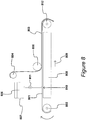
- a roll-to-roll process is illustrated in Figure 8 .
- a first conductive layer 801 is received from a first supply reel 802.
- a second conductive layer 803 is received from a second supply reel 804 and is supported by a roller 805.
- Composite material 806 is retained in liquid form within a supply hopper 807.
- the first conductive material is pulled from its supply reel 802 and is supported by a base unit 808. As the material traverses along the base unit in the direction of arrow 809, composite material in liquid form is received at 810, under the control of a motorised valve 811.
- Roller 805 applies the second conductive material above the composite material which, in an embodiment will have been heated or uv-treated so as to effect evaporation of the solvent or curing before the composition is encapsulated by the second conductive layer 803.
- the three layer laminate is then received by reception reel 812.
- the roll-to-roll process illustrated in Figure 4 facilitates a method of producing a device incorporating the electrically responsive composite material, wherein the composite material is constrained within conductive layers to produce a laminate.
- the composite material is used in a method of manufacturing a pressure sensitive and substantially transparent touch screen, as illustrated in Figure 9 .
- a first substrate is selected and at step 902 a first conductive layer is applied to an internal surface of the first substrate.
- a second substrate is selected and again at step 904 a second conductive layer is applied to an internal surface of the second substrate. Consequently, a contact location between the first conductive layer and the second conductive layer allows a position of contact to be determined.
- a composite material of the type previously described is introduced between the first conductive layer and the second conductive layer.
- the composite material has a resistance that reduces in response to applied pressure such that in addition to identifying xy locations within the plane, it is also possible to determine the degree of pressure applied in the z dimension.
- display screens have been used in electronic devices, such as mobile cellular telephones, gaming devices, still cameras and video cameras. Recently, there has been a move towards providing touch screens in which the output interface and the input interface are effectively combined. In this way, as is well known, it is possible to present a larger interface and therefore achieve greater levels of functionality.
- the present invention allows these ideas to be developed further in that it becomes possible to achieve touch sensitivity upon a touch screen whose optical properties are essentially independent of the electrically active filler material, and may be transparent.
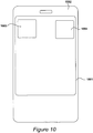
- An electronic device 1001 is shown in Figure 10 .
- the device has a relatively large touch screen 1002.
- Soft buttons 1003, 1004 are included, the activation of which may be determined by identifying a position of contact. Furthermore, other parameters may be controlled by measuring the extent to which these buttons are depressed while at the same time retaining the visual display characteristics through the transparent screen.
- a position sensing device 1101 is shown in an exploded view in Figure 11 and in a cross-sectional view in Figure 12 .
- the cross-sectional view of Figure 12 has been greatly stretched in the direction of its height such that the various layers may be clearly seen. However, it should be understood that, in reality, the inner layers are all microscopically thin.
- the position sensing device 1101 comprises a lower electrically insulating sheet 1102, formed of poly (ethylene terephthalate) (PET) on to which an indium tin oxide (ITO) conductive layer has been applied.
- the first conductive layer 1103 is substantially rectangular in shape and has a highly conductive strip of material 1104, 1105 arranged along each one of two opposing sides of the rectangle.
- the position sensing device 1101 comprises a second sheet of electrically insulating material 1106 (also formed of PET) that has been similarly coated with ITO to form a second electrically conductive layer 1107 and a pair of highly conductive strips 1108 and 1109 arranged along opposing edges of the second conductive layer 1107.
- the second pair of conductive strips 1108 and 1109 are arranged to extend substantially perpendicular to the first set of conductive strips 1104 and 1105.
- a layer of electrically responsive composite material 1110 is arranged between the two electrically conductive layers 1103 and 1107.
- the electrically conductive layer may be formed in accordance with one of the above described methods that make reference to Figures 3 , 4 and 5 .
- an electrically potential is applied to the first conductive strips 1104 and 1105 to produce a potential gradient in a first x direction, indicated by arrow 1111, while voltage measurements are made of the electrical potential appearing at one or both of the second pair of conductive strips 1108 and 1109.
- a force is applied to the upper surface of the upper sheet 1106 and x-coordinate of the potion of the applied force may be determined.
- an electrical potential is applied between the second conductive strips 1108 and 1109 to produce an electrical potential gradient across the second electrically conducting layer 1107 in a second y direction shown by arrow 1112.
- the electrical potential appearing at one or both of the first pair of conductive strips 1104 and 1105 is then measured to determine the y coordinate of any force that is applied to the upper sheet 1107.
- the electrically responsive composite material 1110 provides conduction between the first and second conductive layers 1103 and 1107 at locations where pressure is applied to it. Furthermore, as discussed above, the resistance of the electrically responsive composite material 1110 continuously reduces as applied pressure increases. Consequently, by taking measurements of current through the layer 1110 an indication of the applied pressure can be measured.
- a similar arrangement of layers and electrodes (provided by conductive strips 1104, 1105, 1108 and 1109) is described in the applicants earlier patent application published as GB 2468870A , which also discusses the electrical measurements in detail. However, the position sensor 1101 differs from earlier position sensors, including those of GB 2468870A , in the specific details of the electrically responsive composite material layer 1110.
- each of the sheets 1102 and 1106, the conductive layers 1103 and 1107 and the electrically responsive composite material layer 1110 are substantially transparent or see-through such that the position sensor 1101 maybe used as the pressure sensitive position sensor of a touch screen, such as touch screen 1102 of Figure 10 .
- the sheets or layers may be opaque and the position sensing device 1101 is used as a separate x,y,z input device.
- the electrically response composite material layer 1110 comprises a carrier layer 1301 that, in the present embodiment, is electrically insulating.
- the carrier layer 1301 typically has a length, in direction of 1302, and a width (extending out of the page in Figure 13 ) of several centimetres.
- the carrier layer 1301 has a thickness in direction of arrow 1303 that is relatively thin, typically being less then 10 micro metres, and in the present example is approximately six micrometers.
- the electrically responsive composite material 1110 also comprises a plurality of electrically conductive, or semi-conductive, particles. These particles are agglomerated to form a plurality of agglomerates disbursed within the carrier layer 1110. That is, each of the agglomerates comprises a plurality of the conductive or semi-conductive particles. Seven of the agglomerates 1304, 1305, 1306, 1307, 1308, 1309 and 1310 are illustrated in Figure 13 dispersed within the carrier layer 1301.
- the electrically responsive composite material 1110 is formed by applying (such as by screen printing) a liquid formulation on to a flat planar substrate. Consequently, a lower face 1311 of the composite material 1110 is substantially flat.
- a first plurality of the agglomerates each have a first dimension, in the direction of the thickness 1303 of the carrier layer 1301, that is greater than the thickness of the carrier layer. Consequently, a first plurality of agglomerates 1304, 1305, 1306, 1307, 1308 and 1309 extend outwards from the otherwise generally flat upper surface 1312 of the carrier layer 1301. It is this first plurality of agglomerates that may be employed to provide a conductive path through the thickness of the composite material 1110 during operation of the position sensor 1101. In contrast, agglomerates such as agglomerate 1310 that are completely immersed within the carrier layer 1301 are unable to provide a conductive path.
- a small portion of the position sensing device 1101 is shown in cross-section Figure 14 .
- a first plurality of the agglomerates within the carrier layer have a first dimension, in the direction of the thickness of the carrier layer, that is equal to or greater than the thickness of carrier layer.
- Four agglomerates 1401, 1402, 1403 and 1404 of this first plurality are illustrated in Figure 14 .
- the agglomerates 1401 and 1404 are two of the largest agglomerates with in the electrically responsive composite material and have a first dimension of approximately ten micrometers.
- the upper electrically conductive layer 1107 rests on top of the larger agglomerates, including the agglomerates 1401 and 1404, and thus provides an air gap 1405 between the upper surface 1312 of the carrier layer 1301 and the exposed surface of the second electrically conductive layer 1107. Consequently, when no external forces are applied to the position sensor 1101 it is only the largest of the agglomerates, such as agglomerates 1401 and 1404, that are able to provide any conductive path between the electrically conductive layers 1103 and 1107.
- the upper sheet 1106 becomes deformed in the region of the applied force and compresses the larger ones of the agglomerates that are local to the applied force. For example, on application of a force indicated by arrow 1407 in Figure 14 , the upper sheet 1106 in the region of the force 1407 is pressed towards the lower sheet 1102 and the largest agglomerates, such as 1401 and 1404 become compressed, resulting in the conductivity through these agglomerates increasing.
- the small portion of the position sensor 1101 shown in Figure 14 is shown again in Figure 15 after the application of a force 1407.
- the force 1407 has pushed a portion of the sheet 1106 in the facility of the force 1407 towards the lower sheet 1102 such that the air gap 1405 has been reduced and the first dimension of the largest agglomerates 1401 and 1404 has been reduced. Because these largest agglomerates 1401 and 1404 are compressed the electrical conduction through them has been increased.
- the second electrically conductive layer 1107 has been brought into contact with other agglomerates such as agglomerate 1402 that are thus able to provide electrically conductive paths between the first and the second conductive layers 1103 and 1107.
- a force such as force 1407
- conduction between the two electronically conductive layers 1103 and 1107 increases due to a reduction in resistance for each of the agglomerates that is being compressed and also due to additional agglomerates, such as agglomerate 1402, that are brought into contact with the second conductive layer 1107.
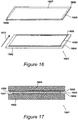
- FIG. 16 An alternative position sensing device 1601 embodying the present invention is shown in the exploded view of Figure 16 and the cross sectional view of Figure 17 . As was the case with Figure 12 , the illustration of Figure 17 has been greatly stretched in order to show the various layers of the position sensing device 1601.
- the position sensing device 1601 has an upper sheet 1606 on which a conductive layer 1607 (of ITO) is provided, along with highly conductive strips 1608 and 1609.
- the upper sheet 1606 is substantially identical to the upper sheet 1106 of position sensing device 1101.
- the position sensing device 1601 has a lower insulating sheet 1602, similar to sheet 1102, and similarly having highly conductive strips 1604 and 1605.
- the lower sheets 1602 differs from the lower sheet 1102 of position sensing device 1101 in that it does not have an electrically conductive layer formed of indium tin oxide. Instead, a layer of electrically responsive composite material 1650 has been applied (by screen printing) directly onto the lower sheet 1602, such that it extends between the highly conductive strips 1604 and 1605.
- the electrically responsive composite material 1650 has a similar form to the electrically conductive composite material 1110 described above, and therefore it comprises agglomerates of smaller conductive particles dispersed within a carrier layer. However, unlike the carrier layer 1301 of electrically conductive composite material 1110, the electrically responsive composite material 1650 has a carrier layer that is itself electrically conductive, being formed of a conductive polymer; in the present case poly(3,4-ethylenedioxythiophene) poly(styrenesulfonate) (PEDOT/PSS).
- PEDOT/PSS poly(3,4-ethylenedioxythiophene) poly(styrenesulfonate)
- the position sensing device 1601 operates in a similar manner to position sensing device 1101. However, in this instance, the carrier layer of the electrically conducting composite material 1650 provides the first conductive layer for providing electrical conduction along the layer, in direction of arrow 1611, while the agglomerates within the carrier layer provide conduction between the carrier layer and the conductive layer 1607 on the upper sheet 1606.
Landscapes
- Engineering & Computer Science (AREA)
- Physics & Mathematics (AREA)
- Theoretical Computer Science (AREA)
- General Engineering & Computer Science (AREA)
- Microelectronics & Electronic Packaging (AREA)
- General Physics & Mathematics (AREA)
- Chemical & Material Sciences (AREA)
- Dispersion Chemistry (AREA)
- Human Computer Interaction (AREA)
- Spectroscopy & Molecular Physics (AREA)
- Position Input By Displaying (AREA)
- Laminated Bodies (AREA)
- Push-Button Switches (AREA)
- Non-Insulated Conductors (AREA)
- Compositions Of Macromolecular Compounds (AREA)
Claims (15)
- Ein elektrisch ansprechbarer Verbundwerkstoff (101, 1110, 1650), einschließlich:einer Trägerschicht (1301) mit einer Länge (1302) sowie einer Breite und einer Stärke (1303), wobei letztere relativ gering im Vergleich zu besagter Länge und besagter Breite ist; sowieeiner Vielzahl von elektrisch leitfähigen oder halbleitenden Partikeln (201), wobei besagte Partikel zu einer Vielzahl von Agglomeraten (104, 1304, 1305, 1306, 1307, 1308, 1309,1310,1401, 1402, 1403, 1404) angehäuft und innerhalb der Trägerschicht verteilt sind, sodass jedes der besagten Agglomerate aus einer Vielfalt besagter Partikel besteht,gekennzeichnet dadurch, dass jedes der besagten Agglomerate eine erste Ausdehnung in Richtung besagter Stärke hat, welche gleich groß wie oder größer als besagte Stärke besagter Trägerschicht ist, sodass jedes der besagten Agglomerate derart ausgerichtet ist, dass es bei angewendetem Druck eine elektrische Leitungsstrecke durch die Stärke besagter Trägerschicht erzeugt, sodass besagter elektrisch ansprechbarer Verbundwerkstoff über einen sich bei Druck verringernden Widerstand verfügt.
- Der elektrisch ansprechbare Verbundwerkstoff entsprechend Patentanspruch 1, gekennzeichnet dadurch, dass
die größte Ausdehnung jedes Agglomerats aus der besagten Vielzahl von Agglomeraten kleiner als 40 Mikrometer ist. - Der elektrisch ansprechbare Verbundwerkstoff aus Patentanspruch 1, gekennzeichnet dadurch, dass
die größte Ausdehnung der Vielzahl von Agglomeraten kleiner als 15 Mikrometer ist. - Der elektrisch ansprechbare Verbundwerkstoff aus Patentanspruch 2 oder Patentanspruch 3, gekennzeichnet dadurch, dass
die größte Ausdehnung jedes Agglomerats aus der besagten Vielzahl von Agglomeraten größer als 5 Mikrometer ist. - Der elektrisch ansprechbare Verbundwerkstoff aus einem jeden der Patentansprüche 1 bis 4, gekennzeichnet dadurch, dass
besagte Trägerschicht ein elektrisch leitfähiges Material enthält, sodass besagte Trägerschicht in Richtung der Länge und Breite besagter Schicht leitfähig ist. - Der elektrisch ansprechbare Verbundwerkstoff aus einem jeden der Patentansprüche 1 bis 5, gekennzeichnet dadurch, dass
besagte Trägerschicht ein Polymer enthält. - Der elektrisch ansprechbare Verbundwerkstoff aus Patentanspruch 6, gekennzeichnet dadurch, dass
besagtes Polymer durchsichtig ist. - Der elektrisch ansprechbare Verbundwerkstoff aus einem jeden der Patentansprüche 1 bis 7, gekennzeichnet dadurch, dass
besagte Agglomerate aus weiteren Partikeln (202) aus einem dielektrischen Material bestehen. - Der elektrisch ansprechbare Verbundwerkstoff aus einem jeden der Patentansprüche 1 bis 8, gekennzeichnet dadurch, dass
besagte Agglomerate halbleitende Partikel enthalten. - Der elektrisch ansprechbare Verbundwerkstoff aus Patentanspruch 9, gekennzeichnet dadurch, dass
besagte halbleitende Partikel Partikel aus Zinnoxid mit Antimon-Dotierung sind. - Eine Vorrichtung zur Positionsbestimmung (1101), einschließlich:des elektrisch ansprechbaren Verbundwerkstoffes (101, 1110, 1650) aus einem jeden der Patentansprüche 1 bis 10;einer ersten leitfähigen Schicht (704, 801, 1103), die entlang besagter Schicht elektrisch leitfähig ist; sowieeiner zweiten leitfähigen Schicht (803, 1107), die entlang besagter Schicht elektrisch leitfähig ist; wobei besagte Agglomerate derart angeordnet sind, dass Leitung zwischen besagter erster leitfähiger Schicht und besagter zweiter leitfähiger Schicht ermöglicht wird.
- Die Vorrichtung zur Positionsbestimmung aus Patentanspruch 11, gekennzeichnet dadurch, dass
die erste Ausdehnung der ersten Vielzahl von Agglomeraten länger als besagte Stärke besagter Trägerschicht ist, und dass die besagte zweite Leitschicht an einer Vielzahl besagter ersten Vielzahl von Agglomeraten liegt, um eine Lücke (1405) zwischen besagter zweiter Leitschicht und besagter Trägerschicht zu schaffen. - Die Vorrichtung zur Positionsbestimmung aus Patentanspruch 11 oder Patentanspruch 12, gekennzeichnet dadurch, dass
besagte Trägerschicht elektrisch leitfähiges Material enthält, sodass besagte Trägerschicht in Richtung der Länge und Breite besagter Trägerschicht leitfähig ist, und dass besagte Trägerschicht besagte erste leitfähige Schicht erzeugt. - Die Vorrichtung zur Positionsbestimmung aus einem jeden der Patentansprüche 11 bis 13, gekennzeichnet dadurch, dass
besagte erste leitfähige Schicht durchsichtig und auf einem ersten durchsichtigen Substrat (701) geformt ist, weiterhin, dass besagte zweite leitfähige Schicht durchsichtig und auf einem zweiten leitfähigen Substrat (702) geformt ist, sowie, dass besagte Trägerschicht durchsichtig ist, sodass die besagte Vorrichtung zur Positionsbestimmung durchsichtig ist. - Die Vorrichtung zur Positionsbestimmung aus einem jeden der Patentansprüche 11 bis 14, gekennzeichnet dadurch, dass
besagte Vorrichtung zur Positionsbestimmung ein druckempfindlicher Positionssensor (1101) eines Touchscreens (1002, 1102) ist.
Applications Claiming Priority (3)
| Application Number | Priority Date | Filing Date | Title |
|---|---|---|---|
| GB201105025A GB201105025D0 (en) | 2011-03-25 | 2011-03-25 | Electrically responsive composite material |
| GB201117492A GB201117492D0 (en) | 2011-03-25 | 2011-10-11 | Composite material |
| PCT/GB2012/000260 WO2012131289A2 (en) | 2011-03-25 | 2012-03-22 | Composite material |
Publications (2)
| Publication Number | Publication Date |
|---|---|
| EP2689431A2 EP2689431A2 (de) | 2014-01-29 |
| EP2689431B1 true EP2689431B1 (de) | 2017-02-01 |
Family
ID=44067353
Family Applications (1)
| Application Number | Title | Priority Date | Filing Date |
|---|---|---|---|
| EP12717435.7A Active EP2689431B1 (de) | 2011-03-25 | 2012-03-22 | Druckempfindliche polymerverbundstoff angepasst für berührungsbildschirm |
Country Status (6)
| Country | Link |
|---|---|
| US (1) | US9546859B2 (de) |
| EP (1) | EP2689431B1 (de) |
| JP (1) | JP6042863B2 (de) |
| KR (1) | KR101980388B1 (de) |
| GB (3) | GB201105025D0 (de) |
| WO (1) | WO2012131289A2 (de) |
Families Citing this family (15)
| Publication number | Priority date | Publication date | Assignee | Title |
|---|---|---|---|---|
| JP6185847B2 (ja) * | 2014-01-07 | 2017-08-23 | 日本写真印刷株式会社 | タッチパネル |
| EP3244179B1 (de) * | 2014-12-24 | 2020-09-23 | Nippon Mektron, Ltd. | Drucksensorelement und drucksensor |
| US20180052547A1 (en) * | 2015-03-30 | 2018-02-22 | Rohm And Haas Electronic Materials Llc | Composite transparent pressure sensing film |
| US20180066126A1 (en) * | 2015-03-30 | 2018-03-08 | Rohm And Haas Electronic Materials Llc | Transparent pressure sensing film with hybrid particles |
| US20180067602A1 (en) * | 2015-03-30 | 2018-03-08 | Rohm And Haas Electronic Materials Llc | Transparent pressure sensing film composition |
| KR102593532B1 (ko) | 2016-06-03 | 2023-10-26 | 삼성디스플레이 주식회사 | 이방성 도전 필름 및 이를 이용한 디스플레이 장치 |
| KR102543477B1 (ko) | 2016-06-10 | 2023-06-16 | 삼성디스플레이 주식회사 | 센서 및 이를 포함하는 표시 장치 |
| KR102628240B1 (ko) | 2016-09-07 | 2024-01-25 | 삼성디스플레이 주식회사 | 입력 센서 및 이를 포함하는 표시 장치 |
| KR102628247B1 (ko) | 2016-09-20 | 2024-01-25 | 삼성디스플레이 주식회사 | 터치 센서 및 이를 포함하는 표시 장치 |
| KR102679070B1 (ko) | 2016-10-17 | 2024-07-02 | 삼성디스플레이 주식회사 | 터치 센서 및 이를 포함하는 표시 장치 |
| KR102050183B1 (ko) * | 2016-11-23 | 2019-11-28 | 선전 구딕스 테크놀로지 컴퍼니, 리미티드 | 힘 측정 방법, 장치 및 기기 |
| US10935445B2 (en) | 2017-01-04 | 2021-03-02 | Mas Innovation (Private) Limited | Wearable touch button assembly |
| GB2561609B (en) * | 2017-04-21 | 2019-12-18 | Peratech Holdco Ltd | Method of producing agglomerates for inclusion in a composite material |
| GB2566267B (en) | 2017-09-06 | 2021-02-17 | Peratech Holdco Ltd | Agglomerating nano-particles |
| GB2585349A (en) | 2019-05-03 | 2021-01-13 | Hilsum Cyril | Force or pressure sensing composite material |
Family Cites Families (17)
| Publication number | Priority date | Publication date | Assignee | Title |
|---|---|---|---|---|
| US4644101A (en) * | 1985-12-11 | 1987-02-17 | At&T Bell Laboratories | Pressure-responsive position sensor |
| US4745301A (en) * | 1985-12-13 | 1988-05-17 | Advanced Micro-Matrix, Inc. | Pressure sensitive electro-conductive materials |
| JPH069378Y2 (ja) * | 1988-04-20 | 1994-03-09 | 日本合成ゴム株式会社 | 導電性エラストマー複合シート |
| JP2897391B2 (ja) * | 1990-10-15 | 1999-05-31 | ジェイエスアール株式会社 | 回路基板装置およびその製造方法 |
| JPH04151899A (ja) * | 1990-10-15 | 1992-05-25 | Cmk Corp | 電磁波シールドプリント配線板の製造方法 |
| US5296837A (en) * | 1992-07-10 | 1994-03-22 | Interlink Electronics, Inc. | Stannous oxide force transducer and composition |
| US5302936A (en) * | 1992-09-02 | 1994-04-12 | Interlink Electronics, Inc. | Conductive particulate force transducer |
| JP3812682B2 (ja) * | 1994-05-10 | 2006-08-23 | 日立化成工業株式会社 | 異方導電性樹脂フィルム状成形物の製造法 |
| AU2176899A (en) | 1998-01-23 | 1999-08-09 | Peratech Ltd | Polymer composition |
| US6951666B2 (en) * | 2001-10-05 | 2005-10-04 | Cabot Corporation | Precursor compositions for the deposition of electrically conductive features |
| US20050062024A1 (en) | 2003-08-06 | 2005-03-24 | Bessette Michael D. | Electrically conductive pressure sensitive adhesives, method of manufacture, and use thereof |
| JP5129935B2 (ja) * | 2006-06-13 | 2013-01-30 | 日東電工株式会社 | シート状複合材料及びその製造方法 |
| KR101102186B1 (ko) * | 2007-01-31 | 2012-01-02 | 히다치 가세고교 가부시끼가이샤 | 감광성 엘리먼트 |
| GB0708702D0 (en) | 2007-05-04 | 2007-06-13 | Peratech Ltd | Polymer composition |
| JP2009135044A (ja) * | 2007-11-30 | 2009-06-18 | Tdk Corp | 透明導電材料及び透明導電体 |
| EP2240286A4 (de) * | 2007-12-20 | 2014-05-21 | Cima Nano Tech Israel Ltd | Transparente leitende beschichtung mit füllermaterial |
| GB2468870B (en) | 2009-03-25 | 2016-08-03 | Peratech Holdco Ltd | Sensor |
-
2011
- 2011-03-25 GB GB201105025A patent/GB201105025D0/en not_active Ceased
- 2011-10-11 GB GB201117492A patent/GB201117492D0/en not_active Ceased
-
2012
- 2012-03-22 JP JP2014500463A patent/JP6042863B2/ja active Active
- 2012-03-22 WO PCT/GB2012/000260 patent/WO2012131289A2/en not_active Ceased
- 2012-03-22 GB GB1318558.2A patent/GB2504412B/en active Active
- 2012-03-22 EP EP12717435.7A patent/EP2689431B1/de active Active
- 2012-03-22 KR KR1020137027988A patent/KR101980388B1/ko active Active
- 2012-03-26 US US14/007,232 patent/US9546859B2/en active Active
Non-Patent Citations (1)
| Title |
|---|
| None * |
Also Published As
| Publication number | Publication date |
|---|---|
| WO2012131289A3 (en) | 2013-03-07 |
| US9546859B2 (en) | 2017-01-17 |
| WO2012131289A2 (en) | 2012-10-04 |
| GB2504412B (en) | 2015-10-28 |
| KR20140051159A (ko) | 2014-04-30 |
| KR101980388B1 (ko) | 2019-05-21 |
| GB201117492D0 (en) | 2011-11-23 |
| US20140109698A1 (en) | 2014-04-24 |
| JP2014515097A (ja) | 2014-06-26 |
| EP2689431A2 (de) | 2014-01-29 |
| GB201318558D0 (en) | 2013-12-04 |
| GB2504412A (en) | 2014-01-29 |
| JP6042863B2 (ja) | 2016-12-14 |
| GB201105025D0 (en) | 2011-05-11 |
Similar Documents
| Publication | Publication Date | Title |
|---|---|---|
| US9546859B2 (en) | Composite material | |
| Kim et al. | Interactive skin display with epidermal stimuli electrode | |
| US8449974B2 (en) | Electrically responsive composite material, a method of manufacture and a transducer produced using said material | |
| US9018030B2 (en) | Transparent force sensor and method of fabrication | |
| US8607651B2 (en) | Hybrid capacitive force sensors | |
| CN102165298B (zh) | 感压传感器 | |
| EP2595039A2 (de) | Eingabe-Anzeigevorrichtung | |
| JP2010086512A (ja) | タッチパネル入力装置のための透明導電層化構造 | |
| CN103365464B (zh) | 触摸面板 | |
| Gao et al. | Inkjet‐printed iontronics for transparent, elastic, and strain‐insensitive touch sensing matrix | |
| JP2014021749A (ja) | 抵抗膜式タッチパネル及びタッチパネル装置 | |
| CN207008580U (zh) | 具有由多个层制造的触摸屏的移动通信设备 | |
| KR102944976B1 (ko) | 압력센서 및 그 제조방법, 압력센서를 구비한 표시장치 | |
| KR20110136144A (ko) | 터치패널용 전극 페이스트 조성물 및 이를 이용한 전극 형성방법 | |
| JP2001296972A (ja) | タッチパネルおよびその製造方法 | |
| US7744782B2 (en) | Transparent conductor | |
| JP2007321131A (ja) | 導電性高分子膜、電極基板およびスイッチ | |
| JP2007324097A (ja) | スイッチおよびその製造方法 | |
| JP2008070938A (ja) | タッチパネル | |
| Dempsey et al. | Printable, Transparent Force Sensing Resistive Materials for Touchscreen Applications | |
| US20180067602A1 (en) | Transparent pressure sensing film composition | |
| JP2015018724A (ja) | 透明導電膜とその製造方法 | |
| KR20190068882A (ko) | 터치 입력 장치 | |
| JP2017052178A (ja) | 積層体及びそれを用いたタッチパネル | |
| JPH06324783A (ja) | 加圧スイッチ装置 |
Legal Events
| Date | Code | Title | Description |
|---|---|---|---|
| PUAI | Public reference made under article 153(3) epc to a published international application that has entered the european phase |
Free format text: ORIGINAL CODE: 0009012 |
|
| 17P | Request for examination filed |
Effective date: 20131018 |
|
| AK | Designated contracting states |
Kind code of ref document: A2 Designated state(s): AL AT BE BG CH CY CZ DE DK EE ES FI FR GB GR HR HU IE IS IT LI LT LU LV MC MK MT NL NO PL PT RO RS SE SI SK SM TR |
|
| DAX | Request for extension of the european patent (deleted) | ||
| 19U | Interruption of proceedings before grant |
Effective date: 20140122 |
|
| 19W | Proceedings resumed before grant after interruption of proceedings |
Effective date: 20151201 |
|
| 17Q | First examination report despatched |
Effective date: 20151207 |
|
| RAP1 | Party data changed (applicant data changed or rights of an application transferred) |
Owner name: PERATECH HOLDCO LIMITED |
|
| GRAP | Despatch of communication of intention to grant a patent |
Free format text: ORIGINAL CODE: EPIDOSNIGR1 |
|
| RIC1 | Information provided on ipc code assigned before grant |
Ipc: G01B 7/00 20060101ALI20160804BHEP Ipc: G06F 3/045 20060101ALI20160804BHEP Ipc: G01B 7/16 20060101ALI20160804BHEP Ipc: G06F 3/041 20060101ALI20160804BHEP Ipc: H01B 1/20 20060101ALI20160804BHEP Ipc: H01C 10/10 20060101AFI20160804BHEP |
|
| INTG | Intention to grant announced |
Effective date: 20160822 |
|
| GRAS | Grant fee paid |
Free format text: ORIGINAL CODE: EPIDOSNIGR3 |
|
| RBV | Designated contracting states (corrected) |
Designated state(s): AL AT BE BG CH CY CZ DE DK EE ES FI FR GR HR HU IE IS IT LI LT LU LV MC MK MT NL NO PL PT RO RS SE SI SK SM TR |
|
| GRAA | (expected) grant |
Free format text: ORIGINAL CODE: 0009210 |
|
| AK | Designated contracting states |
Kind code of ref document: B1 Designated state(s): AL AT BE BG CH CY CZ DE DK EE ES FI FR GR HR HU IE IS IT LI LT LU LV MC MK MT NL NO PL PT RO RS SE SI SK SM TR |
|
| REG | Reference to a national code |
Ref country code: CH Ref legal event code: EP Ref country code: AT Ref legal event code: REF Ref document number: 866150 Country of ref document: AT Kind code of ref document: T Effective date: 20170215 |
|
| REG | Reference to a national code |
Ref country code: IE Ref legal event code: FG4D |
|
| REG | Reference to a national code |
Ref country code: DE Ref legal event code: R096 Ref document number: 602012028252 Country of ref document: DE |
|
| REG | Reference to a national code |
Ref country code: FR Ref legal event code: PLFP Year of fee payment: 6 |
|
| REG | Reference to a national code |
Ref country code: NL Ref legal event code: MP Effective date: 20170201 |
|
| REG | Reference to a national code |
Ref country code: LT Ref legal event code: MG4D |
|
| REG | Reference to a national code |
Ref country code: AT Ref legal event code: MK05 Ref document number: 866150 Country of ref document: AT Kind code of ref document: T Effective date: 20170201 |
|
| PG25 | Lapsed in a contracting state [announced via postgrant information from national office to epo] |
Ref country code: NO Free format text: LAPSE BECAUSE OF FAILURE TO SUBMIT A TRANSLATION OF THE DESCRIPTION OR TO PAY THE FEE WITHIN THE PRESCRIBED TIME-LIMIT Effective date: 20170501 Ref country code: FI Free format text: LAPSE BECAUSE OF FAILURE TO SUBMIT A TRANSLATION OF THE DESCRIPTION OR TO PAY THE FEE WITHIN THE PRESCRIBED TIME-LIMIT Effective date: 20170201 Ref country code: GR Free format text: LAPSE BECAUSE OF FAILURE TO SUBMIT A TRANSLATION OF THE DESCRIPTION OR TO PAY THE FEE WITHIN THE PRESCRIBED TIME-LIMIT Effective date: 20170502 Ref country code: HR Free format text: LAPSE BECAUSE OF FAILURE TO SUBMIT A TRANSLATION OF THE DESCRIPTION OR TO PAY THE FEE WITHIN THE PRESCRIBED TIME-LIMIT Effective date: 20170201 Ref country code: IS Free format text: LAPSE BECAUSE OF FAILURE TO SUBMIT A TRANSLATION OF THE DESCRIPTION OR TO PAY THE FEE WITHIN THE PRESCRIBED TIME-LIMIT Effective date: 20170601 Ref country code: LT Free format text: LAPSE BECAUSE OF FAILURE TO SUBMIT A TRANSLATION OF THE DESCRIPTION OR TO PAY THE FEE WITHIN THE PRESCRIBED TIME-LIMIT Effective date: 20170201 |
|
| PG25 | Lapsed in a contracting state [announced via postgrant information from national office to epo] |
Ref country code: NL Free format text: LAPSE BECAUSE OF FAILURE TO SUBMIT A TRANSLATION OF THE DESCRIPTION OR TO PAY THE FEE WITHIN THE PRESCRIBED TIME-LIMIT Effective date: 20170201 Ref country code: ES Free format text: LAPSE BECAUSE OF FAILURE TO SUBMIT A TRANSLATION OF THE DESCRIPTION OR TO PAY THE FEE WITHIN THE PRESCRIBED TIME-LIMIT Effective date: 20170201 Ref country code: RS Free format text: LAPSE BECAUSE OF FAILURE TO SUBMIT A TRANSLATION OF THE DESCRIPTION OR TO PAY THE FEE WITHIN THE PRESCRIBED TIME-LIMIT Effective date: 20170201 Ref country code: BG Free format text: LAPSE BECAUSE OF FAILURE TO SUBMIT A TRANSLATION OF THE DESCRIPTION OR TO PAY THE FEE WITHIN THE PRESCRIBED TIME-LIMIT Effective date: 20170501 Ref country code: AT Free format text: LAPSE BECAUSE OF FAILURE TO SUBMIT A TRANSLATION OF THE DESCRIPTION OR TO PAY THE FEE WITHIN THE PRESCRIBED TIME-LIMIT Effective date: 20170201 Ref country code: PT Free format text: LAPSE BECAUSE OF FAILURE TO SUBMIT A TRANSLATION OF THE DESCRIPTION OR TO PAY THE FEE WITHIN THE PRESCRIBED TIME-LIMIT Effective date: 20170601 Ref country code: PL Free format text: LAPSE BECAUSE OF FAILURE TO SUBMIT A TRANSLATION OF THE DESCRIPTION OR TO PAY THE FEE WITHIN THE PRESCRIBED TIME-LIMIT Effective date: 20170201 Ref country code: SE Free format text: LAPSE BECAUSE OF FAILURE TO SUBMIT A TRANSLATION OF THE DESCRIPTION OR TO PAY THE FEE WITHIN THE PRESCRIBED TIME-LIMIT Effective date: 20170201 Ref country code: LV Free format text: LAPSE BECAUSE OF FAILURE TO SUBMIT A TRANSLATION OF THE DESCRIPTION OR TO PAY THE FEE WITHIN THE PRESCRIBED TIME-LIMIT Effective date: 20170201 |
|
| PG25 | Lapsed in a contracting state [announced via postgrant information from national office to epo] |
Ref country code: SK Free format text: LAPSE BECAUSE OF FAILURE TO SUBMIT A TRANSLATION OF THE DESCRIPTION OR TO PAY THE FEE WITHIN THE PRESCRIBED TIME-LIMIT Effective date: 20170201 Ref country code: EE Free format text: LAPSE BECAUSE OF FAILURE TO SUBMIT A TRANSLATION OF THE DESCRIPTION OR TO PAY THE FEE WITHIN THE PRESCRIBED TIME-LIMIT Effective date: 20170201 Ref country code: RO Free format text: LAPSE BECAUSE OF FAILURE TO SUBMIT A TRANSLATION OF THE DESCRIPTION OR TO PAY THE FEE WITHIN THE PRESCRIBED TIME-LIMIT Effective date: 20170201 Ref country code: CZ Free format text: LAPSE BECAUSE OF FAILURE TO SUBMIT A TRANSLATION OF THE DESCRIPTION OR TO PAY THE FEE WITHIN THE PRESCRIBED TIME-LIMIT Effective date: 20170201 Ref country code: IT Free format text: LAPSE BECAUSE OF FAILURE TO SUBMIT A TRANSLATION OF THE DESCRIPTION OR TO PAY THE FEE WITHIN THE PRESCRIBED TIME-LIMIT Effective date: 20170201 |
|
| REG | Reference to a national code |
Ref country code: CH Ref legal event code: PL |
|
| REG | Reference to a national code |
Ref country code: DE Ref legal event code: R097 Ref document number: 602012028252 Country of ref document: DE |
|
| PG25 | Lapsed in a contracting state [announced via postgrant information from national office to epo] |
Ref country code: MC Free format text: LAPSE BECAUSE OF FAILURE TO SUBMIT A TRANSLATION OF THE DESCRIPTION OR TO PAY THE FEE WITHIN THE PRESCRIBED TIME-LIMIT Effective date: 20170201 Ref country code: DK Free format text: LAPSE BECAUSE OF FAILURE TO SUBMIT A TRANSLATION OF THE DESCRIPTION OR TO PAY THE FEE WITHIN THE PRESCRIBED TIME-LIMIT Effective date: 20170201 Ref country code: SM Free format text: LAPSE BECAUSE OF FAILURE TO SUBMIT A TRANSLATION OF THE DESCRIPTION OR TO PAY THE FEE WITHIN THE PRESCRIBED TIME-LIMIT Effective date: 20170201 |
|
| PLBE | No opposition filed within time limit |
Free format text: ORIGINAL CODE: 0009261 |
|
| STAA | Information on the status of an ep patent application or granted ep patent |
Free format text: STATUS: NO OPPOSITION FILED WITHIN TIME LIMIT |
|
| REG | Reference to a national code |
Ref country code: IE Ref legal event code: MM4A |
|
| 26N | No opposition filed |
Effective date: 20171103 |
|
| PG25 | Lapsed in a contracting state [announced via postgrant information from national office to epo] |
Ref country code: LU Free format text: LAPSE BECAUSE OF NON-PAYMENT OF DUE FEES Effective date: 20170322 |
|
| PG25 | Lapsed in a contracting state [announced via postgrant information from national office to epo] |
Ref country code: IE Free format text: LAPSE BECAUSE OF NON-PAYMENT OF DUE FEES Effective date: 20170322 Ref country code: CH Free format text: LAPSE BECAUSE OF NON-PAYMENT OF DUE FEES Effective date: 20170331 Ref country code: SI Free format text: LAPSE BECAUSE OF FAILURE TO SUBMIT A TRANSLATION OF THE DESCRIPTION OR TO PAY THE FEE WITHIN THE PRESCRIBED TIME-LIMIT Effective date: 20170201 Ref country code: LI Free format text: LAPSE BECAUSE OF NON-PAYMENT OF DUE FEES Effective date: 20170331 |
|
| REG | Reference to a national code |
Ref country code: BE Ref legal event code: MM Effective date: 20170331 |
|
| REG | Reference to a national code |
Ref country code: FR Ref legal event code: PLFP Year of fee payment: 7 |
|
| PG25 | Lapsed in a contracting state [announced via postgrant information from national office to epo] |
Ref country code: BE Free format text: LAPSE BECAUSE OF NON-PAYMENT OF DUE FEES Effective date: 20170331 |
|
| PG25 | Lapsed in a contracting state [announced via postgrant information from national office to epo] |
Ref country code: MT Free format text: LAPSE BECAUSE OF NON-PAYMENT OF DUE FEES Effective date: 20170322 |
|
| PG25 | Lapsed in a contracting state [announced via postgrant information from national office to epo] |
Ref country code: HU Free format text: LAPSE BECAUSE OF FAILURE TO SUBMIT A TRANSLATION OF THE DESCRIPTION OR TO PAY THE FEE WITHIN THE PRESCRIBED TIME-LIMIT; INVALID AB INITIO Effective date: 20120322 |
|
| PG25 | Lapsed in a contracting state [announced via postgrant information from national office to epo] |
Ref country code: CY Free format text: LAPSE BECAUSE OF NON-PAYMENT OF DUE FEES Effective date: 20170201 |
|
| PG25 | Lapsed in a contracting state [announced via postgrant information from national office to epo] |
Ref country code: MK Free format text: LAPSE BECAUSE OF FAILURE TO SUBMIT A TRANSLATION OF THE DESCRIPTION OR TO PAY THE FEE WITHIN THE PRESCRIBED TIME-LIMIT Effective date: 20170201 |
|
| PG25 | Lapsed in a contracting state [announced via postgrant information from national office to epo] |
Ref country code: TR Free format text: LAPSE BECAUSE OF FAILURE TO SUBMIT A TRANSLATION OF THE DESCRIPTION OR TO PAY THE FEE WITHIN THE PRESCRIBED TIME-LIMIT Effective date: 20170201 |
|
| PG25 | Lapsed in a contracting state [announced via postgrant information from national office to epo] |
Ref country code: AL Free format text: LAPSE BECAUSE OF FAILURE TO SUBMIT A TRANSLATION OF THE DESCRIPTION OR TO PAY THE FEE WITHIN THE PRESCRIBED TIME-LIMIT Effective date: 20170201 |
|
| PGFP | Annual fee paid to national office [announced via postgrant information from national office to epo] |
Ref country code: FR Payment date: 20220202 Year of fee payment: 11 |
|
| PG25 | Lapsed in a contracting state [announced via postgrant information from national office to epo] |
Ref country code: FR Free format text: LAPSE BECAUSE OF NON-PAYMENT OF DUE FEES Effective date: 20230331 |
|
| REG | Reference to a national code |
Ref country code: DE Ref legal event code: R088 Ref document number: 602012028252 Country of ref document: DE |
|
| REG | Reference to a national code |
Ref country code: DE Ref legal event code: R082 Ref document number: 602012028252 Country of ref document: DE Representative=s name: LICHTI - PATENTANWAELTE PARTNERSCHAFT MBB, DE Ref country code: DE Ref legal event code: R081 Ref document number: 602012028252 Country of ref document: DE Owner name: PERATECH IP LIMITED, CATTERICK GARRISON, GB Free format text: FORMER OWNER: PERATECH HOLDCO LIMITED, RICHMOND, GB |
|
| PGFP | Annual fee paid to national office [announced via postgrant information from national office to epo] |
Ref country code: DE Payment date: 20250903 Year of fee payment: 14 |