EP2689269B1 - Fabrication d'un détecteur d'imagerie spectrale - Google Patents
Fabrication d'un détecteur d'imagerie spectrale Download PDFInfo
- Publication number
- EP2689269B1 EP2689269B1 EP20120713356 EP12713356A EP2689269B1 EP 2689269 B1 EP2689269 B1 EP 2689269B1 EP 20120713356 EP20120713356 EP 20120713356 EP 12713356 A EP12713356 A EP 12713356A EP 2689269 B1 EP2689269 B1 EP 2689269B1
- Authority
- EP
- European Patent Office
- Prior art keywords
- photosensor
- scintillator
- substrate
- row
- coupling
- Prior art date
- Legal status (The legal status is an assumption and is not a legal conclusion. Google has not performed a legal analysis and makes no representation as to the accuracy of the status listed.)
- Active
Links
- 238000000701 chemical imaging Methods 0.000 title description 5
- 238000004519 manufacturing process Methods 0.000 title description 2
- 239000000758 substrate Substances 0.000 claims description 76
- 238000000034 method Methods 0.000 claims description 19
- 230000008878 coupling Effects 0.000 claims description 12
- 238000010168 coupling process Methods 0.000 claims description 12
- 238000005859 coupling reaction Methods 0.000 claims description 12
- 239000000463 material Substances 0.000 claims description 11
- 230000000295 complement effect Effects 0.000 claims description 8
- 230000005855 radiation Effects 0.000 description 23
- 238000002591 computed tomography Methods 0.000 description 9
- 238000003384 imaging method Methods 0.000 description 7
- 230000003595 spectral effect Effects 0.000 description 6
- 230000037361 pathway Effects 0.000 description 4
- 230000000712 assembly Effects 0.000 description 3
- 238000000429 assembly Methods 0.000 description 3
- 239000000853 adhesive Substances 0.000 description 2
- 230000001070 adhesive effect Effects 0.000 description 2
- 230000004075 alteration Effects 0.000 description 2
- 238000003491 array Methods 0.000 description 2
- 238000001514 detection method Methods 0.000 description 2
- 238000012986 modification Methods 0.000 description 2
- 230000004048 modification Effects 0.000 description 2
- 230000003287 optical effect Effects 0.000 description 1
- 229920001690 polydopamine Polymers 0.000 description 1
- 238000000926 separation method Methods 0.000 description 1
- 229910052710 silicon Inorganic materials 0.000 description 1
- 239000010703 silicon Substances 0.000 description 1
- 239000007787 solid Substances 0.000 description 1
Images


Classifications
-
- G—PHYSICS
- G01—MEASURING; TESTING
- G01T—MEASUREMENT OF NUCLEAR OR X-RADIATION
- G01T1/00—Measuring X-radiation, gamma radiation, corpuscular radiation, or cosmic radiation
- G01T1/16—Measuring radiation intensity
- G01T1/20—Measuring radiation intensity with scintillation detectors
- G01T1/2006—Measuring radiation intensity with scintillation detectors using a combination of a scintillator and photodetector which measures the means radiation intensity
-
- G—PHYSICS
- G01—MEASURING; TESTING
- G01T—MEASUREMENT OF NUCLEAR OR X-RADIATION
- G01T1/00—Measuring X-radiation, gamma radiation, corpuscular radiation, or cosmic radiation
- G01T1/29—Measurement performed on radiation beams, e.g. position or section of the beam; Measurement of spatial distribution of radiation
- G01T1/2914—Measurement of spatial distribution of radiation
- G01T1/2985—In depth localisation, e.g. using positron emitters; Tomographic imaging (longitudinal and transverse section imaging; apparatus for radiation diagnosis sequentially in different planes, steroscopic radiation diagnosis)
-
- H—ELECTRICITY
- H01—ELECTRIC ELEMENTS
- H01L—SEMICONDUCTOR DEVICES NOT COVERED BY CLASS H10
- H01L31/00—Semiconductor devices sensitive to infrared radiation, light, electromagnetic radiation of shorter wavelength or corpuscular radiation and specially adapted either for the conversion of the energy of such radiation into electrical energy or for the control of electrical energy by such radiation; Processes or apparatus specially adapted for the manufacture or treatment thereof or of parts thereof; Details thereof
- H01L31/02—Details
- H01L31/0232—Optical elements or arrangements associated with the device
- H01L31/02322—Optical elements or arrangements associated with the device comprising luminescent members, e.g. fluorescent sheets upon the device
Claims (13)
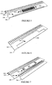
- Procédé, comprenant :l'obtention d'un substrat photo-capteur (236) comportant deux surfaces principales opposées (302 et 308), dans lequel une des deux surfaces principales opposées comprend au moins une rangée de photo-capteur (230) d'au moins un élément photo-capteur (232, 234), et le substrat photo-capteur obtenu possède une épaisseur égale ou supérieure à cent microns ;le couplage optique d'un réseau scintillateur (310) au substrat photo-capteur, dans lequel le réseau scintillateur comprend au moins une rangée de scintillateur complémentaire (224) d'au moins un élément scintillateur complémentaire (226, 228), et l'au moins une rangée de scintillateur complémentaire est optiquement couplée à l'au moins une rangée de photo-capteur (230) et l'au moins un élément scintillateur complémentaire est optiquement couplé à l'au moins un élément photo-capteur ; etl'amincissement du substrat photo-capteur qui est optiquement couplé au scintillateur,la production d'un substrat photo-capteur aminci qui est optiquement couplé au scintillateur avec une épaisseur inférieure à cent microns.
- Procédé selon la revendication 1, dans lequel l'une des deux surfaces principales opposées comprend une première région (304) et une seconde région (306), dans lequel l'au moins une rangée de photo-capteur de l'au moins un élément photo-capteur est couplée seulement à la première région et le scintillateur est couplé à l'au moins une rangée de photo-capteur de l'au moins un élément photo-capteur et la seconde région.
- Procédé selon la revendication 2, dans lequel le scintillateur comprend un premier scintillateur optiquement couplé à l'au moins une rangée de photo-capteur de l'au moins un élément photo-capteur et un autre matériau couplé à la seconde région.
- Procédé selon une quelconque des revendications 1 à 3, comprenant en outre :le couplage d'au moins un parmi des éléments électroniques de traitement (240) ou des broches électriquement conductrices (238) au substrat photo-capteur avant le couplage optique du scintillateur au substrat photo-capteur, dans lequel l'au moins un parmi les éléments électroniques de traitement ou les broches électriquement conductrices sont disposés entre le substrat photo-capteur et le scintillateur après le couplage du scintillateur au substrat photo-capteur.
- Procédé selon la revendication 4, dans lequel l'au moins une rangée de photo-capteur de l'au moins un élément photo-capteur et l'au moins un parmi les éléments électroniques de traitement ou les broches électriquement conductrices sont disposés sur une même surface (508) du substrat photo-capteur.
- Procédé selon la revendication 4, dans lequel au moins un parmi les éléments électroniques de traitement ou les broches électriquement conductrices sont disposés sur une surface (606) dans un évidement (604) du réseau scintillateur.
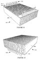
- Procédé selon une quelconque des revendications 4 à 6, dans lequel le substrat photo-capteur fait partie d'une feuille de matériau comprenant une pluralité de substrat photo-capteur, et comprenant en outre :le couplage d'une pluralité d'éléments électroniques de traitement respectivement à la pluralité de substrats photo-capteurs ; etla dépose physique du substrat photo-capteur à partir de la feuille de matériau après au moins le couplage des éléments électroniques de traitement au substrat photo-capteur.
- Procédé selon une quelconque des revendications 1 à 7, comprenant en outre :le placement du substrat photo-capteur sur une structure de support avant le couplage d'au moins le scintillateur au substrat photo-capteur et le couplage d'au moins un composant (244, 240, 238, 704) sur le substrat photo-capteur avec le substrat photo-capteur sur la structure de support.
- Procédé selon la revendication 1, comprenant en outre :le couplage électrique de l'au moins un élément photo-capteur à des éléments électroniques de traitement situés extérieurement au substrat photo-capteur.
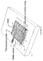
- Procédé selon une quelconque des revendications 1 à 9, comprenant en outre :le couplage mécanique et électrique d'une pluralité des substrats photo-capteurs amincis à un substrat de carreau détecteur (242), formant ainsi un carreau détecteur (220).
- Procédé selon la revendication 10, comprenant en outre :le couplage mécanique et électrique d'une pluralité des carreaux détecteurs pour former un réseau détecteur.
- Procédé selon une quelconque des revendications 1 à 9, dans lequel l'épaisseur du substrat photo-capteur aminci est dans une plage de vingt-cinq à soixante-quinze microns.
- Procédé selon une quelconque des revendications 1 à 10, dans lequel l'épaisseur du substrat photo-capteur aminci est de l'ordre de cinquante microns.
Applications Claiming Priority (2)
| Application Number | Priority Date | Filing Date | Title |
|---|---|---|---|
| US201161467044P | 2011-03-24 | 2011-03-24 | |
| PCT/IB2012/051300 WO2012127403A2 (fr) | 2011-03-24 | 2012-03-19 | Détecteur d'imagerie spectrale |
Publications (2)
| Publication Number | Publication Date |
|---|---|
| EP2689269A2 EP2689269A2 (fr) | 2014-01-29 |
| EP2689269B1 true EP2689269B1 (fr) | 2015-05-13 |
Family
ID=45937487
Family Applications (1)
| Application Number | Title | Priority Date | Filing Date |
|---|---|---|---|
| EP20120713356 Active EP2689269B1 (fr) | 2011-03-24 | 2012-03-19 | Fabrication d'un détecteur d'imagerie spectrale |
Country Status (6)
| Country | Link |
|---|---|
| US (2) | US9281422B2 (fr) |
| EP (1) | EP2689269B1 (fr) |
| JP (1) | JP6071077B2 (fr) |
| CN (1) | CN103443652B (fr) |
| RU (1) | RU2595795C2 (fr) |
| WO (1) | WO2012127403A2 (fr) |
Families Citing this family (17)
| Publication number | Priority date | Publication date | Assignee | Title |
|---|---|---|---|---|
| JP6243518B2 (ja) | 2013-05-16 | 2017-12-06 | コーニンクレッカ フィリップス エヌ ヴェKoninklijke Philips N.V. | イメージング検出器 |
| EP3069170B1 (fr) | 2013-11-15 | 2020-04-15 | Koninklijke Philips N.V. | Photodétecteur organique à double face sur un substrat souple |
| EP3120383B1 (fr) * | 2015-01-15 | 2017-11-29 | Koninklijke Philips N.V. | Ensemble de module détecteur d'imagerie |
| WO2018077681A1 (fr) * | 2016-10-26 | 2018-05-03 | Koninklijke Philips N.V. | Détecteur à scintillation de rayonnement à interconnexion intégrée par trou traversant |
| US10247007B2 (en) | 2017-05-02 | 2019-04-02 | General Electric Company | Airfoil shape for a turbine rotor blade |
| US10352170B2 (en) | 2017-05-02 | 2019-07-16 | General Electric Company | Airfoil shape for a turbine rotor blade |
| US10422227B2 (en) | 2017-05-02 | 2019-09-24 | General Electric Company | Airfoil shape for a turbine rotor blade |
| US10280774B2 (en) | 2017-05-03 | 2019-05-07 | General Electric Company | Turbine nozzle airfoil profile |
| US10415406B2 (en) | 2017-05-03 | 2019-09-17 | General Electric Company | Turbine nozzle airfoil profile |
| US10408072B2 (en) | 2017-05-08 | 2019-09-10 | General Electric Company | Turbine nozzle airfoil profile |
| US10533440B2 (en) | 2017-05-15 | 2020-01-14 | General Electric Company | Turbine nozzle airfoil profile |
| US10436034B2 (en) | 2017-05-15 | 2019-10-08 | General Electric Company | Airfoil shape for a turbine rotor blade |
| WO2019041172A1 (fr) * | 2017-08-30 | 2019-03-07 | Shenzhen United Imaging Healthcare Co., Ltd. | Système, procédé et module de détecteur pour imagerie tep |
| US11181488B2 (en) | 2017-08-31 | 2021-11-23 | Koninklijke Philips N.V. | Multi-layer detector with a monolithic scintillator |
| DE102018200845B4 (de) | 2018-01-19 | 2021-05-06 | Siemens Healthcare Gmbh | Montageverfahren für die Herstellung eines Röntgendetektors, Röntgendetektor und Röntgengerät |
| KR20210099604A (ko) * | 2018-12-06 | 2021-08-12 | 아나로그 디바이시즈 인코포레이티드 | 차폐된 통합된 디바이스 패키지들 |
| IT201900010638A1 (it) * | 2019-07-02 | 2021-01-02 | St Microelectronics Srl | Rilevatore di radiazione a scintillatore e dosimetro corrispondente |
Family Cites Families (44)
| Publication number | Priority date | Publication date | Assignee | Title |
|---|---|---|---|---|
| JPS57172272A (en) * | 1981-04-17 | 1982-10-23 | Toshiba Corp | Multichannel type radiation detector |
| US5043582A (en) * | 1985-12-11 | 1991-08-27 | General Imagining Corporation | X-ray imaging system and solid state detector therefor |
| JPS62231222A (ja) | 1986-03-31 | 1987-10-09 | Nitto Electric Ind Co Ltd | 液晶配向膜形成用溶液 |
| US5179284A (en) * | 1991-08-21 | 1993-01-12 | General Electric Company | Solid state radiation imager having a reflective and protective coating |
| RU2123710C1 (ru) * | 1996-01-31 | 1998-12-20 | Товарищество с ограниченной ответственностью "Медтех" | Матричный рентгеновский приемник |
| FR2758630B1 (fr) * | 1997-01-21 | 1999-04-09 | Thomson Tubes Electroniques | Procede de scellement etanche d'un detecteur de rayonnement a l'etat solide et detecteur obtenu par ce procede |
| US6114703A (en) * | 1997-10-21 | 2000-09-05 | The Regents Of The University Of California | High resolution scintillation detector with semiconductor readout |
| DE19841423C1 (de) * | 1998-09-10 | 1999-12-30 | Siemens Ag | Strahlendetektor, insbesondere eines Computertomographen |
| US6522715B2 (en) * | 2000-12-29 | 2003-02-18 | Ge Medical Systems Global Technology Company Llc | High density flex interconnect for CT detectors |
| JP2003084066A (ja) * | 2001-04-11 | 2003-03-19 | Nippon Kessho Kogaku Kk | 放射線検出器用部品、放射線検出器および放射線検出装置 |
| JP5038209B2 (ja) * | 2001-04-11 | 2012-10-03 | 日本結晶光学株式会社 | 放射線検出装置 |
| US6510195B1 (en) * | 2001-07-18 | 2003-01-21 | Koninklijke Philips Electronics, N.V. | Solid state x-radiation detector modules and mosaics thereof, and an imaging method and apparatus employing the same |
| US6895077B2 (en) * | 2001-11-21 | 2005-05-17 | University Of Massachusetts Medical Center | System and method for x-ray fluoroscopic imaging |
| EP1543350A1 (fr) * | 2002-09-18 | 2005-06-22 | Koninklijke Philips Electronics N.V. | Detecteur de radiations |
| US7019304B2 (en) * | 2003-10-06 | 2006-03-28 | General Electric Company | Solid-state radiation imager with back-side irradiation |
| CN1890580B (zh) * | 2003-12-09 | 2010-09-01 | 皇家飞利浦电子股份有限公司 | X射线检测器的屏蔽 |
| US7075091B2 (en) | 2004-01-29 | 2006-07-11 | Ge Medical Systems Global Technology Company, Llc | Apparatus for detecting ionizing radiation |
| JP2006058168A (ja) * | 2004-08-20 | 2006-03-02 | Hamamatsu Photonics Kk | 放射線撮像素子および放射線撮像方法 |
| DE102004052452B4 (de) * | 2004-10-28 | 2008-05-29 | Siemens Ag | Strahlungsdetektor zur Erfassung von Strahlung |
| JP2006145431A (ja) * | 2004-11-22 | 2006-06-08 | Ge Medical Systems Global Technology Co Llc | 放射線検出器、放射線撮像装置、放射線ct装置及び放射線検出器の製造方法 |
| RU2411542C2 (ru) * | 2005-04-22 | 2011-02-10 | Конинклейке Филипс Электроникс Н.В. | Цифровой кремниевый фотоумножитель для врп-пэт |
| EP1877832B1 (fr) | 2005-04-26 | 2018-02-21 | Koninklijke Philips N.V. | Reseau de detecteurs pour tomographie spectrale par ordinateur |
| EP1876955B1 (fr) * | 2005-04-26 | 2016-11-23 | Koninklijke Philips N.V. | Detecteur a double niveau pour tomographie spectrale par ordinateur |
| US7399972B2 (en) * | 2005-06-09 | 2008-07-15 | Nihon Kessho Kogaku Co., Ltd. | Component for radiation detector and radiation detector |
| CN101278208A (zh) | 2005-10-05 | 2008-10-01 | 皇家飞利浦电子股份有限公司 | 使用薄电路的计算机断层摄影探测器 |
| WO2007117799A2 (fr) * | 2006-03-30 | 2007-10-18 | Koninklijke Philips Electronics, N.V. | Réseau de détecteurs de radiations |
| US7692156B1 (en) * | 2006-08-23 | 2010-04-06 | Radiation Monitoring Devices, Inc. | Beam-oriented pixellated scintillators for radiation imaging |
| US7608837B2 (en) * | 2006-11-24 | 2009-10-27 | Tower Semiconductor Ltd. | High resolution integrated X-ray CMOS image sensor |
| WO2008132634A2 (fr) * | 2007-04-25 | 2008-11-06 | Koninklijke Philips Electronics N.V. | Détecteur de rayonnement ayant un couplage optique laminé séparé |
| WO2009060349A2 (fr) * | 2007-11-09 | 2009-05-14 | Koninklijke Philips Electronics N.V. | Protection de scintillateurs hygroscopiques |
| JP2009147212A (ja) * | 2007-12-17 | 2009-07-02 | Nippon Kessho Kogaku Kk | 光検出器および光検出器を用いた光検出装置 |
| RU2487373C2 (ru) | 2007-12-21 | 2013-07-10 | Конинклейке Филипс Электроникс Н.В. | Чувствительный к излучению детектор со сцинтиллятором в композиционной смоле |
| WO2009098753A1 (fr) * | 2008-02-04 | 2009-08-13 | Shimadzu Corporation | Détecteur de rayonnement et système tomographique équipé de ce dernier |
| US20110056618A1 (en) * | 2008-06-05 | 2011-03-10 | Hiromichi Tonami | Method of manufacturing radiation detector |
| US7737409B2 (en) * | 2008-06-12 | 2010-06-15 | Analog Devices, Inc. | Silicon detector and method for constructing silicon detectors |
| WO2010010608A1 (fr) * | 2008-07-22 | 2010-01-28 | 株式会社島津製作所 | Procédé de fabrication d’un équipement tomographique à rayonnement |
| CN105044758B (zh) * | 2008-11-18 | 2022-06-14 | 皇家飞利浦电子股份有限公司 | 光谱成像检测器 |
| US8718226B2 (en) * | 2008-11-21 | 2014-05-06 | Trixell | Assembly method for a tiled radiation detector |
| KR101497498B1 (ko) * | 2008-12-19 | 2015-03-03 | 삼성전자주식회사 | 방사선 신호의 투과 영상을 획득하는 방법 및 장치 |
| JP5247486B2 (ja) * | 2009-01-16 | 2013-07-24 | 浜松ホトニクス株式会社 | 裏面入射型フォトダイオードアレイ及び放射線検出器 |
| US8373132B2 (en) * | 2009-02-06 | 2013-02-12 | Koninklijke Philips Electronics N. V. | Radiation detector with a stack of scintillator elements and photodiode arrays |
| US9164700B2 (en) | 2009-03-05 | 2015-10-20 | Sandisk Il Ltd | System for optimizing the transfer of stored content in response to a triggering event |
| US8466421B2 (en) * | 2010-07-30 | 2013-06-18 | Varian Medical Systems Inc. | Radiation detector with multiple operating schemes |
| JP5422581B2 (ja) * | 2011-01-31 | 2014-02-19 | 富士フイルム株式会社 | 放射線画像検出装置及びその製造方法 |
-
2012
- 2012-03-19 US US14/006,703 patent/US9281422B2/en active Active
- 2012-03-19 WO PCT/IB2012/051300 patent/WO2012127403A2/fr active Application Filing
- 2012-03-19 CN CN201280014657.2A patent/CN103443652B/zh active Active
- 2012-03-19 JP JP2014500514A patent/JP6071077B2/ja active Active
- 2012-03-19 EP EP20120713356 patent/EP2689269B1/fr active Active
- 2012-03-19 RU RU2013147397/28A patent/RU2595795C2/ru not_active IP Right Cessation
-
2016
- 2016-02-03 US US15/014,297 patent/US9599725B2/en active Active
Also Published As
| Publication number | Publication date |
|---|---|
| RU2595795C2 (ru) | 2016-08-27 |
| JP6071077B2 (ja) | 2017-02-01 |
| WO2012127403A3 (fr) | 2012-12-27 |
| EP2689269A2 (fr) | 2014-01-29 |
| US9599725B2 (en) | 2017-03-21 |
| CN103443652A (zh) | 2013-12-11 |
| WO2012127403A2 (fr) | 2012-09-27 |
| RU2013147397A (ru) | 2015-04-27 |
| JP2014513279A (ja) | 2014-05-29 |
| US9281422B2 (en) | 2016-03-08 |
| US20140015081A1 (en) | 2014-01-16 |
| US20160154121A1 (en) | 2016-06-02 |
| CN103443652B (zh) | 2017-02-15 |
Similar Documents
| Publication | Publication Date | Title |
|---|---|---|
| EP2689269B1 (fr) | Fabrication d'un détecteur d'imagerie spectrale | |
| JP5455620B2 (ja) | 放射線検出器および当該検出器を含む装置 | |
| US20080253507A1 (en) | Computed Tomography Detector Using Thin Circuits | |
| US20160320495A1 (en) | Apparatus for detecting x-rays | |
| EP3532872B1 (fr) | Détecteur à scintillation de rayonnement à interconnexion intégrée par trou traversant | |
| US20130292574A1 (en) | Multi-layer horizontal computed tomography (ct) detector array with at least one thin photosensor array layer disposed between at least two scintillator array layers | |
| CN101214154A (zh) | Ct探测器模块构造 | |
| RU2647206C1 (ru) | Сенсорное устройство и система визуализации для обнаружения сигналов излучения | |
| US10283557B2 (en) | Radiation detector assembly | |
| KR102624385B1 (ko) | 모듈식 x선 검출기(modular x-ray detector) | |
| WO2017116523A1 (fr) | Ensemble détecteur de rayonnement | |
| US20210278553A1 (en) | Three-dimensional solid state imaging photodetector | |
| EP3155663B1 (fr) | Circuit asic de détecteur d'imagerie modulaire | |
| JP7034635B2 (ja) | 検出器モジュール、放射線検出器、x線コンピュータ断層撮影装置及び放射線検出器の製造方法 |
Legal Events
| Date | Code | Title | Description |
|---|---|---|---|
| PUAI | Public reference made under article 153(3) epc to a published international application that has entered the european phase |
Free format text: ORIGINAL CODE: 0009012 |
|
| 17P | Request for examination filed |
Effective date: 20131024 |
|
| AK | Designated contracting states |
Kind code of ref document: A2 Designated state(s): AL AT BE BG CH CY CZ DE DK EE ES FI FR GB GR HR HU IE IS IT LI LT LU LV MC MK MT NL NO PL PT RO RS SE SI SK SM TR |
|
| DAX | Request for extension of the european patent (deleted) | ||
| 17Q | First examination report despatched |
Effective date: 20140725 |
|
| GRAP | Despatch of communication of intention to grant a patent |
Free format text: ORIGINAL CODE: EPIDOSNIGR1 |
|
| INTG | Intention to grant announced |
Effective date: 20141105 |
|
| GRAS | Grant fee paid |
Free format text: ORIGINAL CODE: EPIDOSNIGR3 |
|
| GRAA | (expected) grant |
Free format text: ORIGINAL CODE: 0009210 |
|
| AK | Designated contracting states |
Kind code of ref document: B1 Designated state(s): AL AT BE BG CH CY CZ DE DK EE ES FI FR GB GR HR HU IE IS IT LI LT LU LV MC MK MT NL NO PL PT RO RS SE SI SK SM TR |
|
| REG | Reference to a national code |
Ref country code: GB Ref legal event code: FG4D |
|
| REG | Reference to a national code |
Ref country code: CH Ref legal event code: EP |
|
| REG | Reference to a national code |
Ref country code: IE Ref legal event code: FG4D |
|
| REG | Reference to a national code |
Ref country code: AT Ref legal event code: REF Ref document number: 727038 Country of ref document: AT Kind code of ref document: T Effective date: 20150615 |
|
| REG | Reference to a national code |
Ref country code: DE Ref legal event code: R096 Ref document number: 602012007312 Country of ref document: DE Effective date: 20150625 |
|
| REG | Reference to a national code |
Ref country code: AT Ref legal event code: MK05 Ref document number: 727038 Country of ref document: AT Kind code of ref document: T Effective date: 20150513 |
|
| REG | Reference to a national code |
Ref country code: NL Ref legal event code: MP Effective date: 20150513 |
|
| REG | Reference to a national code |
Ref country code: LT Ref legal event code: MG4D |
|
| PG25 | Lapsed in a contracting state [announced via postgrant information from national office to epo] |
Ref country code: PT Free format text: LAPSE BECAUSE OF FAILURE TO SUBMIT A TRANSLATION OF THE DESCRIPTION OR TO PAY THE FEE WITHIN THE PRESCRIBED TIME-LIMIT Effective date: 20150914 Ref country code: HR Free format text: LAPSE BECAUSE OF FAILURE TO SUBMIT A TRANSLATION OF THE DESCRIPTION OR TO PAY THE FEE WITHIN THE PRESCRIBED TIME-LIMIT Effective date: 20150513 Ref country code: NO Free format text: LAPSE BECAUSE OF FAILURE TO SUBMIT A TRANSLATION OF THE DESCRIPTION OR TO PAY THE FEE WITHIN THE PRESCRIBED TIME-LIMIT Effective date: 20150813 Ref country code: ES Free format text: LAPSE BECAUSE OF FAILURE TO SUBMIT A TRANSLATION OF THE DESCRIPTION OR TO PAY THE FEE WITHIN THE PRESCRIBED TIME-LIMIT Effective date: 20150513 Ref country code: FI Free format text: LAPSE BECAUSE OF FAILURE TO SUBMIT A TRANSLATION OF THE DESCRIPTION OR TO PAY THE FEE WITHIN THE PRESCRIBED TIME-LIMIT Effective date: 20150513 Ref country code: LT Free format text: LAPSE BECAUSE OF FAILURE TO SUBMIT A TRANSLATION OF THE DESCRIPTION OR TO PAY THE FEE WITHIN THE PRESCRIBED TIME-LIMIT Effective date: 20150513 |
|
| PG25 | Lapsed in a contracting state [announced via postgrant information from national office to epo] |
Ref country code: GR Free format text: LAPSE BECAUSE OF FAILURE TO SUBMIT A TRANSLATION OF THE DESCRIPTION OR TO PAY THE FEE WITHIN THE PRESCRIBED TIME-LIMIT Effective date: 20150814 Ref country code: BG Free format text: LAPSE BECAUSE OF FAILURE TO SUBMIT A TRANSLATION OF THE DESCRIPTION OR TO PAY THE FEE WITHIN THE PRESCRIBED TIME-LIMIT Effective date: 20150813 Ref country code: RS Free format text: LAPSE BECAUSE OF FAILURE TO SUBMIT A TRANSLATION OF THE DESCRIPTION OR TO PAY THE FEE WITHIN THE PRESCRIBED TIME-LIMIT Effective date: 20150513 Ref country code: LV Free format text: LAPSE BECAUSE OF FAILURE TO SUBMIT A TRANSLATION OF THE DESCRIPTION OR TO PAY THE FEE WITHIN THE PRESCRIBED TIME-LIMIT Effective date: 20150513 Ref country code: AT Free format text: LAPSE BECAUSE OF FAILURE TO SUBMIT A TRANSLATION OF THE DESCRIPTION OR TO PAY THE FEE WITHIN THE PRESCRIBED TIME-LIMIT Effective date: 20150513 Ref country code: IS Free format text: LAPSE BECAUSE OF FAILURE TO SUBMIT A TRANSLATION OF THE DESCRIPTION OR TO PAY THE FEE WITHIN THE PRESCRIBED TIME-LIMIT Effective date: 20150913 |
|
| PG25 | Lapsed in a contracting state [announced via postgrant information from national office to epo] |
Ref country code: DK Free format text: LAPSE BECAUSE OF FAILURE TO SUBMIT A TRANSLATION OF THE DESCRIPTION OR TO PAY THE FEE WITHIN THE PRESCRIBED TIME-LIMIT Effective date: 20150513 Ref country code: EE Free format text: LAPSE BECAUSE OF FAILURE TO SUBMIT A TRANSLATION OF THE DESCRIPTION OR TO PAY THE FEE WITHIN THE PRESCRIBED TIME-LIMIT Effective date: 20150513 |
|
| REG | Reference to a national code |
Ref country code: DE Ref legal event code: R097 Ref document number: 602012007312 Country of ref document: DE |
|
| PG25 | Lapsed in a contracting state [announced via postgrant information from national office to epo] |
Ref country code: CZ Free format text: LAPSE BECAUSE OF FAILURE TO SUBMIT A TRANSLATION OF THE DESCRIPTION OR TO PAY THE FEE WITHIN THE PRESCRIBED TIME-LIMIT Effective date: 20150513 Ref country code: RO Free format text: LAPSE BECAUSE OF NON-PAYMENT OF DUE FEES Effective date: 20150513 Ref country code: PL Free format text: LAPSE BECAUSE OF FAILURE TO SUBMIT A TRANSLATION OF THE DESCRIPTION OR TO PAY THE FEE WITHIN THE PRESCRIBED TIME-LIMIT Effective date: 20150513 Ref country code: SK Free format text: LAPSE BECAUSE OF FAILURE TO SUBMIT A TRANSLATION OF THE DESCRIPTION OR TO PAY THE FEE WITHIN THE PRESCRIBED TIME-LIMIT Effective date: 20150513 |
|
| PLBE | No opposition filed within time limit |
Free format text: ORIGINAL CODE: 0009261 |
|
| STAA | Information on the status of an ep patent application or granted ep patent |
Free format text: STATUS: NO OPPOSITION FILED WITHIN TIME LIMIT |
|
| 26N | No opposition filed |
Effective date: 20160216 |
|
| PG25 | Lapsed in a contracting state [announced via postgrant information from national office to epo] |
Ref country code: IT Free format text: LAPSE BECAUSE OF FAILURE TO SUBMIT A TRANSLATION OF THE DESCRIPTION OR TO PAY THE FEE WITHIN THE PRESCRIBED TIME-LIMIT Effective date: 20150513 |
|
| PG25 | Lapsed in a contracting state [announced via postgrant information from national office to epo] |
Ref country code: SI Free format text: LAPSE BECAUSE OF FAILURE TO SUBMIT A TRANSLATION OF THE DESCRIPTION OR TO PAY THE FEE WITHIN THE PRESCRIBED TIME-LIMIT Effective date: 20150513 |
|
| PG25 | Lapsed in a contracting state [announced via postgrant information from national office to epo] |
Ref country code: BE Free format text: LAPSE BECAUSE OF FAILURE TO SUBMIT A TRANSLATION OF THE DESCRIPTION OR TO PAY THE FEE WITHIN THE PRESCRIBED TIME-LIMIT Effective date: 20150513 |
|
| PG25 | Lapsed in a contracting state [announced via postgrant information from national office to epo] |
Ref country code: LU Free format text: LAPSE BECAUSE OF FAILURE TO SUBMIT A TRANSLATION OF THE DESCRIPTION OR TO PAY THE FEE WITHIN THE PRESCRIBED TIME-LIMIT Effective date: 20160319 Ref country code: MC Free format text: LAPSE BECAUSE OF FAILURE TO SUBMIT A TRANSLATION OF THE DESCRIPTION OR TO PAY THE FEE WITHIN THE PRESCRIBED TIME-LIMIT Effective date: 20150513 |
|
| REG | Reference to a national code |
Ref country code: CH Ref legal event code: PL |
|
| GBPC | Gb: european patent ceased through non-payment of renewal fee |
Effective date: 20160319 |
|
| REG | Reference to a national code |
Ref country code: IE Ref legal event code: MM4A |
|
| REG | Reference to a national code |
Ref country code: FR Ref legal event code: ST Effective date: 20161130 |
|
| PG25 | Lapsed in a contracting state [announced via postgrant information from national office to epo] |
Ref country code: IE Free format text: LAPSE BECAUSE OF NON-PAYMENT OF DUE FEES Effective date: 20160319 Ref country code: FR Free format text: LAPSE BECAUSE OF NON-PAYMENT OF DUE FEES Effective date: 20160331 Ref country code: GB Free format text: LAPSE BECAUSE OF NON-PAYMENT OF DUE FEES Effective date: 20160319 Ref country code: CH Free format text: LAPSE BECAUSE OF NON-PAYMENT OF DUE FEES Effective date: 20160331 Ref country code: LI Free format text: LAPSE BECAUSE OF NON-PAYMENT OF DUE FEES Effective date: 20160331 |
|
| PG25 | Lapsed in a contracting state [announced via postgrant information from national office to epo] |
Ref country code: NL Free format text: LAPSE BECAUSE OF FAILURE TO SUBMIT A TRANSLATION OF THE DESCRIPTION OR TO PAY THE FEE WITHIN THE PRESCRIBED TIME-LIMIT Effective date: 20150513 Ref country code: SE Free format text: LAPSE BECAUSE OF FAILURE TO SUBMIT A TRANSLATION OF THE DESCRIPTION OR TO PAY THE FEE WITHIN THE PRESCRIBED TIME-LIMIT Effective date: 20150513 |
|
| PG25 | Lapsed in a contracting state [announced via postgrant information from national office to epo] |
Ref country code: MT Free format text: LAPSE BECAUSE OF FAILURE TO SUBMIT A TRANSLATION OF THE DESCRIPTION OR TO PAY THE FEE WITHIN THE PRESCRIBED TIME-LIMIT Effective date: 20150513 |
|
| PG25 | Lapsed in a contracting state [announced via postgrant information from national office to epo] |
Ref country code: SM Free format text: LAPSE BECAUSE OF FAILURE TO SUBMIT A TRANSLATION OF THE DESCRIPTION OR TO PAY THE FEE WITHIN THE PRESCRIBED TIME-LIMIT Effective date: 20150513 Ref country code: CY Free format text: LAPSE BECAUSE OF FAILURE TO SUBMIT A TRANSLATION OF THE DESCRIPTION OR TO PAY THE FEE WITHIN THE PRESCRIBED TIME-LIMIT Effective date: 20150513 Ref country code: HU Free format text: LAPSE BECAUSE OF FAILURE TO SUBMIT A TRANSLATION OF THE DESCRIPTION OR TO PAY THE FEE WITHIN THE PRESCRIBED TIME-LIMIT; INVALID AB INITIO Effective date: 20120319 |
|
| PG25 | Lapsed in a contracting state [announced via postgrant information from national office to epo] |
Ref country code: TR Free format text: LAPSE BECAUSE OF FAILURE TO SUBMIT A TRANSLATION OF THE DESCRIPTION OR TO PAY THE FEE WITHIN THE PRESCRIBED TIME-LIMIT Effective date: 20150513 Ref country code: MT Free format text: LAPSE BECAUSE OF FAILURE TO SUBMIT A TRANSLATION OF THE DESCRIPTION OR TO PAY THE FEE WITHIN THE PRESCRIBED TIME-LIMIT Effective date: 20160331 Ref country code: MK Free format text: LAPSE BECAUSE OF FAILURE TO SUBMIT A TRANSLATION OF THE DESCRIPTION OR TO PAY THE FEE WITHIN THE PRESCRIBED TIME-LIMIT Effective date: 20150513 |
|
| REG | Reference to a national code |
Ref country code: DE Ref legal event code: R084 Ref document number: 602012007312 Country of ref document: DE |
|
| PG25 | Lapsed in a contracting state [announced via postgrant information from national office to epo] |
Ref country code: AL Free format text: LAPSE BECAUSE OF FAILURE TO SUBMIT A TRANSLATION OF THE DESCRIPTION OR TO PAY THE FEE WITHIN THE PRESCRIBED TIME-LIMIT Effective date: 20150513 |
|
| PGFP | Annual fee paid to national office [announced via postgrant information from national office to epo] |
Ref country code: DE Payment date: 20220628 Year of fee payment: 12 |