EP2669944A2 - Halbleitergehäuse und gestapeltes Halbleiterpaket - Google Patents
Halbleitergehäuse und gestapeltes Halbleiterpaket Download PDFInfo
- Publication number
- EP2669944A2 EP2669944A2 EP13168859.0A EP13168859A EP2669944A2 EP 2669944 A2 EP2669944 A2 EP 2669944A2 EP 13168859 A EP13168859 A EP 13168859A EP 2669944 A2 EP2669944 A2 EP 2669944A2
- Authority
- EP
- European Patent Office
- Prior art keywords
- land
- wiring
- semiconductor package
- lands
- signal terminal
- Prior art date
- Legal status (The legal status is an assumption and is not a legal conclusion. Google has not performed a legal analysis and makes no representation as to the accuracy of the status listed.)
- Withdrawn
Links
Images

Classifications
-
- H—ELECTRICITY
- H10—SEMICONDUCTOR DEVICES; ELECTRIC SOLID-STATE DEVICES NOT OTHERWISE PROVIDED FOR
- H10W—GENERIC PACKAGES, INTERCONNECTIONS, CONNECTORS OR OTHER CONSTRUCTIONAL DETAILS OF DEVICES COVERED BY CLASS H10
- H10W72/00—Interconnections or connectors in packages
- H10W72/90—Bond pads, in general
-
- H—ELECTRICITY
- H05—ELECTRIC TECHNIQUES NOT OTHERWISE PROVIDED FOR
- H05K—PRINTED CIRCUITS; CASINGS OR CONSTRUCTIONAL DETAILS OF ELECTRIC APPARATUS; MANUFACTURE OF ASSEMBLAGES OF ELECTRICAL COMPONENTS
- H05K1/00—Printed circuits
- H05K1/18—Printed circuits structurally associated with non-printed electric components
- H05K1/181—Printed circuits structurally associated with non-printed electric components associated with surface mounted components
-
- H—ELECTRICITY
- H10—SEMICONDUCTOR DEVICES; ELECTRIC SOLID-STATE DEVICES NOT OTHERWISE PROVIDED FOR
- H10W—GENERIC PACKAGES, INTERCONNECTIONS, CONNECTORS OR OTHER CONSTRUCTIONAL DETAILS OF DEVICES COVERED BY CLASS H10
- H10W70/00—Package substrates; Interposers; Redistribution layers [RDL]
- H10W70/60—Insulating or insulated package substrates; Interposers; Redistribution layers
- H10W70/62—Insulating or insulated package substrates; Interposers; Redistribution layers characterised by their interconnections
- H10W70/65—Shapes or dispositions of interconnections
-
- H—ELECTRICITY
- H10—SEMICONDUCTOR DEVICES; ELECTRIC SOLID-STATE DEVICES NOT OTHERWISE PROVIDED FOR
- H10W—GENERIC PACKAGES, INTERCONNECTIONS, CONNECTORS OR OTHER CONSTRUCTIONAL DETAILS OF DEVICES COVERED BY CLASS H10
- H10W90/00—Package configurations
-
- H—ELECTRICITY
- H10—SEMICONDUCTOR DEVICES; ELECTRIC SOLID-STATE DEVICES NOT OTHERWISE PROVIDED FOR
- H10W—GENERIC PACKAGES, INTERCONNECTIONS, CONNECTORS OR OTHER CONSTRUCTIONAL DETAILS OF DEVICES COVERED BY CLASS H10
- H10W70/00—Package substrates; Interposers; Redistribution layers [RDL]
- H10W70/60—Insulating or insulated package substrates; Interposers; Redistribution layers
-
- H—ELECTRICITY
- H10—SEMICONDUCTOR DEVICES; ELECTRIC SOLID-STATE DEVICES NOT OTHERWISE PROVIDED FOR
- H10W—GENERIC PACKAGES, INTERCONNECTIONS, CONNECTORS OR OTHER CONSTRUCTIONAL DETAILS OF DEVICES COVERED BY CLASS H10
- H10W70/00—Package substrates; Interposers; Redistribution layers [RDL]
- H10W70/60—Insulating or insulated package substrates; Interposers; Redistribution layers
- H10W70/62—Insulating or insulated package substrates; Interposers; Redistribution layers characterised by their interconnections
- H10W70/63—Vias, e.g. via plugs
-
- H—ELECTRICITY
- H10—SEMICONDUCTOR DEVICES; ELECTRIC SOLID-STATE DEVICES NOT OTHERWISE PROVIDED FOR
- H10W—GENERIC PACKAGES, INTERCONNECTIONS, CONNECTORS OR OTHER CONSTRUCTIONAL DETAILS OF DEVICES COVERED BY CLASS H10
- H10W72/00—Interconnections or connectors in packages
- H10W72/071—Connecting or disconnecting
- H10W72/075—Connecting or disconnecting of bond wires
- H10W72/07551—Connecting or disconnecting of bond wires characterised by changes in properties of the bond wires during the connecting
- H10W72/07553—Connecting or disconnecting of bond wires characterised by changes in properties of the bond wires during the connecting changes in shapes
-
- H—ELECTRICITY
- H10—SEMICONDUCTOR DEVICES; ELECTRIC SOLID-STATE DEVICES NOT OTHERWISE PROVIDED FOR
- H10W—GENERIC PACKAGES, INTERCONNECTIONS, CONNECTORS OR OTHER CONSTRUCTIONAL DETAILS OF DEVICES COVERED BY CLASS H10
- H10W72/00—Interconnections or connectors in packages
- H10W72/20—Bump connectors, e.g. solder bumps or copper pillars; Dummy bumps; Thermal bumps
- H10W72/29—Bond pads specially adapted therefor
-
- H—ELECTRICITY
- H10—SEMICONDUCTOR DEVICES; ELECTRIC SOLID-STATE DEVICES NOT OTHERWISE PROVIDED FOR
- H10W—GENERIC PACKAGES, INTERCONNECTIONS, CONNECTORS OR OTHER CONSTRUCTIONAL DETAILS OF DEVICES COVERED BY CLASS H10
- H10W72/00—Interconnections or connectors in packages
- H10W72/50—Bond wires
- H10W72/531—Shapes of wire connectors
- H10W72/537—Multiple bond wires having different shapes
-
- H—ELECTRICITY
- H10—SEMICONDUCTOR DEVICES; ELECTRIC SOLID-STATE DEVICES NOT OTHERWISE PROVIDED FOR
- H10W—GENERIC PACKAGES, INTERCONNECTIONS, CONNECTORS OR OTHER CONSTRUCTIONAL DETAILS OF DEVICES COVERED BY CLASS H10
- H10W74/00—Encapsulations, e.g. protective coatings
-
- H—ELECTRICITY
- H10—SEMICONDUCTOR DEVICES; ELECTRIC SOLID-STATE DEVICES NOT OTHERWISE PROVIDED FOR
- H10W—GENERIC PACKAGES, INTERCONNECTIONS, CONNECTORS OR OTHER CONSTRUCTIONAL DETAILS OF DEVICES COVERED BY CLASS H10
- H10W74/00—Encapsulations, e.g. protective coatings
- H10W74/10—Encapsulations, e.g. protective coatings characterised by their shape or disposition
- H10W74/111—Encapsulations, e.g. protective coatings characterised by their shape or disposition the semiconductor body being completely enclosed
- H10W74/114—Encapsulations, e.g. protective coatings characterised by their shape or disposition the semiconductor body being completely enclosed by a substrate and the encapsulations
- H10W74/117—Encapsulations, e.g. protective coatings characterised by their shape or disposition the semiconductor body being completely enclosed by a substrate and the encapsulations the substrate having spherical bumps for external connection
-
- H—ELECTRICITY
- H10—SEMICONDUCTOR DEVICES; ELECTRIC SOLID-STATE DEVICES NOT OTHERWISE PROVIDED FOR
- H10W—GENERIC PACKAGES, INTERCONNECTIONS, CONNECTORS OR OTHER CONSTRUCTIONAL DETAILS OF DEVICES COVERED BY CLASS H10
- H10W90/00—Package configurations
- H10W90/701—Package configurations characterised by the relative positions of pads or connectors relative to package parts
- H10W90/721—Package configurations characterised by the relative positions of pads or connectors relative to package parts of bump connectors
- H10W90/722—Package configurations characterised by the relative positions of pads or connectors relative to package parts of bump connectors between stacked chips
-
- H—ELECTRICITY
- H10—SEMICONDUCTOR DEVICES; ELECTRIC SOLID-STATE DEVICES NOT OTHERWISE PROVIDED FOR
- H10W—GENERIC PACKAGES, INTERCONNECTIONS, CONNECTORS OR OTHER CONSTRUCTIONAL DETAILS OF DEVICES COVERED BY CLASS H10
- H10W90/00—Package configurations
- H10W90/701—Package configurations characterised by the relative positions of pads or connectors relative to package parts
- H10W90/721—Package configurations characterised by the relative positions of pads or connectors relative to package parts of bump connectors
- H10W90/724—Package configurations characterised by the relative positions of pads or connectors relative to package parts of bump connectors between a chip and a stacked insulating package substrate, interposer or RDL
-
- H—ELECTRICITY
- H10—SEMICONDUCTOR DEVICES; ELECTRIC SOLID-STATE DEVICES NOT OTHERWISE PROVIDED FOR
- H10W—GENERIC PACKAGES, INTERCONNECTIONS, CONNECTORS OR OTHER CONSTRUCTIONAL DETAILS OF DEVICES COVERED BY CLASS H10
- H10W90/00—Package configurations
- H10W90/701—Package configurations characterised by the relative positions of pads or connectors relative to package parts
- H10W90/751—Package configurations characterised by the relative positions of pads or connectors relative to package parts of bond wires
- H10W90/754—Package configurations characterised by the relative positions of pads or connectors relative to package parts of bond wires between a chip and a stacked insulating package substrate, interposer or RDL
Definitions
- the present invention relates to a semiconductor package that includes a printed wiring board having a semiconductor element mounted thereon, and to a stacked semiconductor package having a package on package (PoP) structure.
- a semiconductor package that includes a printed wiring board having a semiconductor element mounted thereon, and to a stacked semiconductor package having a package on package (PoP) structure.
- PoP package on package
- a stacked semiconductor package having a PoP structure As one form of a semiconductor package, a stacked semiconductor package having a PoP structure is known (see Japanese Patent Application Laid-Open No. 2011-14757 ). This is a structure in which an upper semiconductor package (for example, a package having a DDR memory mounted thereon) is stacked on a lower semiconductor package (for example, a package having a system LSI mounted thereon).
- an upper semiconductor package for example, a package having a DDR memory mounted thereon
- a lower semiconductor package for example, a package having a system LSI mounted thereon
- the upper semiconductor package includes an upper semiconductor chip as a semiconductor element, and an upper printed wiring board having the upper semiconductor chip mounted thereon.
- the lower semiconductor package includes a lower semiconductor chip as a semiconductor element, and a lower printed wiring board having the lower semiconductor chip mounted thereon. Communication between the lower semiconductor chip and the upper semiconductor chip is made through transmission lines formed by solder joining lands of the lower printed wiring board and lands of the upper printed wiring board.
- communication between semiconductor chips requires multiple transmission lines.
- 8-bit communication is made between a system LSI and a DDR memory
- the system is more sophisticated in functionality, and the number of the transmission lines used for communication between the upper and lower semiconductor chips is far above 100.
- Bus circuits or differential circuits provided in a semiconductor element are formed so as to have the same circuit characteristics.
- the bus wirings or the differential signal wirings as the transmission lines are required to have the same transmission line characteristics.
- the length of a wiring that extends from a signal terminal of the semiconductor element to a land varies depending on the position of the land, and thus, the length of the wiring varies, and, due to difference in parasitic inductance caused thereby, the transmission line characteristics vary. If the transmission line characteristics vary among wirings, in a semiconductor element on a signal receiving side, the waveform varies among multiple signals, and thus, it is difficult to ensure synchronization of the signals.
- an object of the present invention is to reduce difference in transmission line characteristics due to difference in wiring length.
- a stacked semiconductor package including: a first semiconductor package including: a first semiconductor element having a first signal terminal and a second signal terminal; and a first wiring board having the first semiconductor element mounted on one surface thereof, and having multiple lands for external connection formed on another surface thereof, the multiple lands for external connection being electrically connected to an outside, the one surface of the first wiring board having provided thereon: a first land and a second land for solder joining; a first wiring for electrically connecting the first signal terminal and the first land; and a second wiring for electrically connecting the second signal terminal and the second land; a second semiconductor package stacked on the first semiconductor package, the second semiconductor package including: a second semiconductor element; and a second wiring board having the second semiconductor element mounted on one surface thereof, and having a third land for connection and a fourth land for connection formed on another surface thereof, the third land for connection and the fourth land for connection being electrically connected to the first land for connection and the second land for connection provided on the first wiring board, respectively; and
- a parasitic capacitance generated at the second land is larger than a parasitic capacitance generated at the first land, and thus, difference in transmission line characteristics due to difference in wiring length can be reduced to ensure synchronization of signals transmitted through the wirings.
- FIG. 1 is a sectional view of a printed circuit board according to a first embodiment of the present invention.
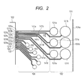
- FIG. 2 is a plan view illustrating a surface layer of a lower interposer according to the first embodiment of the present invention.
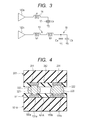
- FIG. 3 is an equivalent circuit diagram of a first transmission line and a second transmission line according to the first embodiment of the present invention.
- FIG. 4 is a sectional view of a principal part of a stacked semiconductor package according to a second embodiment of the present invention.
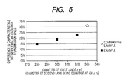
- FIG. 5 is a graph showing difference in characteristics between the first transmission line and the second transmission line.
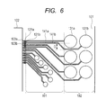
- FIG. 6 is a plan view illustrating a surface layer of a lower interposer in Comparative Example.
- FIG. 1 is a sectional view illustrating a schematic structure of a printed circuit board including a stacked semiconductor package according to a first embodiment of the present invention.
- a printed circuit board 500 includes a stacked semiconductor package 300 and a motherboard 400 having the stacked semiconductor package 300 mounted thereon. The stacked semiconductor package 300 and the motherboard 400 are joined together by multiple lower solder balls 320.
- the stacked semiconductor package 300 is a stacked semiconductor package having a PoP structure.
- the stacked semiconductor package 300 includes a lower semiconductor package 100 as a first semiconductor package and an upper semiconductor package 200 as a second semiconductor package that is stacked on the lower semiconductor package 100.
- the lower semiconductor package 100 and the upper semiconductor package 200 are joined together by multiple upper solder balls 310.
- the lower semiconductor package 100 includes a lower interposer 101 as a first printed wiring board and a lower semiconductor chip 102 as a first semiconductor element that is mounted on the lower interposer 101.
- the lower interposer 101 is formed into the shape of a rectangle (for example, into the shape of a square) as seen from a direction perpendicular to the plane of the lower interposer 101.
- the lower semiconductor chip 102 is also formed into the shape of a rectangle (for example, into the shape of a square) as seen from a direction perpendicular to the plane of the lower semiconductor chip 102.
- the upper semiconductor package 200 includes an upper interposer 201 as a second printed wiring board and an upper semiconductor chip 202 as a second semiconductor element that is mounted on the upper interposer 201.
- the upper interposer 201 is formed into the shape of a rectangle (for example, into the shape of a square) as seen from a direction perpendicular to the plane of the upper interposer 201.
- the upper semiconductor chip 202 is also formed into the shape of a rectangle (for example, into the shape of a square) as seen from a direction perpendicular to the plane of the upper semiconductor chip 202.
- the lower semiconductor chip 102 is, for example, an LSI
- the upper semiconductor chip 202 is, for example, a DDR memory.
- the lower interposer 101, the solder balls 310 as an upper solder joint portion, and the upper interposer 201 form transmission lines used for communication between the lower semiconductor chip 102 and the upper semiconductor chip 202.
- two surface layers 111 and 112 of the lower interposer 101 are wiring layers having multiple wirings formed thereon.
- the lower semiconductor chip 102 is mounted on the surface layer 111 of the two surface layers 111 and 112 of the lower interposer 101.
- FIG. 2 is a plan view illustrating the surface layer 111 of the lower interposer 101.
- the lower semiconductor chip 102 has multiple signal terminals 103a to 103f and 104.
- the lower interposer 101 has lands 121a to 121f and 122 for multiple semiconductor chips, which are formed on the surface layer 111, and are solder joined to the signal terminals 103a to 103f and 104, respectively.
- the signal terminals 103a to 103f are for communication with the upper semiconductor chip 202 of the upper semiconductor package 200, while the signal terminals 104 are for communication with a semiconductor element (not shown) mounted on the motherboard 400 illustrated in FIG. 1 .
- the lower interposer 101 has multiple lands 131a to 131f for solder joining, which are formed on the surface layer 111.
- the lower interposer 101 further has multiple wirings 141a to 141f (wiring pattern) that are formed on the surface layer 111 and electrically connect the lands 121a to 121f for a semiconductor chip and the lands 131a to 131f, respectively.
- the wirings 141a to 141f are electrically connected to the signal terminals 103a to 103f through the lands 121a to 121f for a semiconductor chip, respectively.
- the lands 121a to 121f for a semiconductor chip, the lands 131a to 131f, and the wirings 141a to 141f are formed of the same conductive material and are patterned by etching.
- the lower interposer 101 has multiple via lands 151 that are formed on the surface layer 111, and multiple wirings 152 (wiring pattern) that electrically connect the lands 122 for a semiconductor chip and the via lands 151, respectively.
- the wirings 152 are electrically connected to the signal terminals 104 through the lands 122 for a semiconductor chip, respectively.
- the lower interposer 101 includes, in an inner layer thereof, a ground pattern 161, multiple via lands 153, and via holes 154 that electrically connect the via lands 153.
- the ground pattern 161 is formed in a wiring layer 113 that is adjacent to the surface layer 111 through an insulator 171 (for example, an epoxy resin) that forms an insulating layer, and is arranged so as to be opposed to the lands 131a to 131f.
- the lower interposer 101 has multiple external connection lands 155 for solder joining, which are formed on the surface layer 112, and are electrically connected to the via lands 151 on the surface layer 111 through the via lands 153 and the via holes 154 in the inner layer, respectively.
- the lower interposer 101 has solder resists 181 and 182 that are formed on the surface layers 111 and 112, respectively, and cover the wirings 141a to 141f and 152 and the lands 131a to 131f, 151, and 155 on the surface layers 111 and 112.
- the lands 131a to 131f and 155 on the surface layers 111 and 112, respectively, have exposed areas that are controlled by openings provided in the solder resists 181 and 182, respectively.
- the solder balls 310 and 320 are connected to the lands 131a to 131f and 155, respectively, through the openings.
- Two surface layers 211 and 212 of the upper interposer 201 are wiring layers having multiple wirings formed therein.
- the upper semiconductor chip 202 is mounted on the surface layer 211 of the two surface layers 211 and 212 of the upper interposer 201.
- the upper interposer 201 has multiple wire lands 221 and via lands 222 that are formed in the surface layer 211, and the via lands 222 are electrically connected to the wire lands 221, respectively. Further, the upper interposer 201 has multiple lands 231 for solder joining and via lands 223 that are formed in the surface layer 212, and the via lands 223 are electrically connected to the lands 231, respectively. The via lands 222 in the surface layer 211 and the via lands 223 in the surface layer 212 are electrically connected through via holes 224, respectively.
- the upper semiconductor chip 202 and the wire lands 221 are electrically connected through wires 241.
- the upper semiconductor chip 202 and the wires 241 are encapsulated in an encapsulating resin 291.
- the upper interposer 201 has solder resists 281 and 282 that are formed on the surface layers 211 and 212, respectively, and cover the wirings in the surface layers 211 and 212.
- the lands 231 in the surface layer 212 have exposed areas that are controlled by openings provided in the solder resist 282, and the solder balls 310 as the upper solder joint portion are connected to the lands 231, respectively, through the openings.
- the lands 131 of the lower interposer 101 and the lands 231 of the upper interposer 201 are opposed to each other and are solder joined to each other by the upper solder balls 310 as the solder joint portion.
- the lands 121 for a semiconductor chip, the wirings 141, the lands 131, the upper solder balls 310, the lands 231, the via lands 222 and 223, the via holes 224, the wire lands 221, and the wires 241 form the transmission lines that connect the semiconductor chips 102 and 202.
- the signal terminals 103a to 103f of the lower semiconductor chip 102 are terminals that output data signals, and the signal terminals 103e and 103f are terminals that output strobe signals having opposite phases. Therefore, the wirings 141a to 141d are bus wirings used for transmitting data signals, and the wirings 141e and 141f are differential signal wirings used for transmitting strobe signals.
- the widths of the wirings 141a to 141f are the same, and are, for example, 25 ⁇ m.
- clearance which is equal to or larger than the width of the wirings 141a to 141f, is provided around the wirings 141a to 141f so that a short-circuit is not caused between the wirings 141a to 141f or between the wirings 141a to 141f and the lands 131a to 131f.
- the lands 131a to 131f are in peripheral arrangement in which the lands 131a to 131f are arranged in a lattice-like manner in a land region 192 located outside a wiring region 191.
- the surfaces of the lands 131a to 131f are formed in the shape of a circle.
- the land region 192 is a region between an end 101a of the interposer 101 and ends of the lands on the semiconductor chip 102 side.
- the lands 131a to 131f are arranged in a lattice-like manner with equal pitches in the land region 192.
- the pitches are, for example, 0.4 mm.
- lands 131a to 131f are divided into lands arranged on the inside (on the semiconductor chip side) (first lands) 131a, 131c, and 131e and lands arranged on the outside (on the interposer end side) (second lands) 131b, 131d, and 131f.
- the wiring region 191 is a region between the ends of the lands on the semiconductor chip 102 side and the lands 121 for a semiconductor chip.
- the bus wirings 141a to 141d and the differential signal wirings 141e and 141f are arranged in the wiring region 191. Further, the via lands 151 used for connection with the motherboard 400 are arranged in the wiring region 191.
- the bus wirings 141b and 141d are respectively connected to, among the lands, the lands 131b and 131d (second lands) arranged on the end 101a side of the interposer 101. Therefore, the lengths of the bus wirings 141b and 141d are larger by at least the pitch than the lengths of the bus wirings 141a and 141c (first wirings) that are respectively connected to, among the lands, the lands 131a and 131c (first lands) arranged on the semiconductor chip 102 side.
- the differential signal wiring 141f (second wiring) is connected to, among the lands, the land 131f (second land) arranged on the end 101a side of the interposer 101. Therefore, the length of the differential signal wiring 141f is larger by at least the pitch than the length of the differential signal wiring 141e (first wiring) that is connected to, among the lands, the land 131e (first land) arranged on the semiconductor chip 102 side.
- each of the surface areas of the lands 131b, 131d, and 131f is larger than each of the surface areas of the lands 131a, 131c, and 131e.
- the diameter of the lands 131b, 131d, and 131f is larger than the diameter of the lands 131a, 131c, and 131e.
- the wiring 141a (141c, 141e) and the land 131a (131c, 131e) form a first transmission line.
- the wiring 141b (141d, 141f) and the land 131b (131d, 131f) form a second transmission line.
- FIG. 3 is an equivalent circuit diagram of the first and second transmission lines according to the first embodiment of the present invention.
- the semiconductor chip 102 includes transmitting circuits 102a and 102b as bus circuits.
- the transmitting circuit 102a outputs a data signal from the signal terminal 103a as a first signal terminal.
- the transmitting circuit 102b outputs a data signal from the signal terminal 103b as a second signal terminal.
- the wirings are structured to have a fine line shape. For example, while the width is 25 ⁇ m and the thickness is 25 ⁇ m, the length is several millimeters. In this wiring structure, the inductance is proportional to the length.
- the value of a parasitic inductance 14 of the wiring 141a as the first wiring is represented by La.
- the length of the wiring 141b as the second wiring is larger than that of the wiring 141a, and thus, the inductance of the wiring 141b is higher by the parasitic inductance corresponding to the difference in wiring length.
- the value of the parasitic inductance corresponding to the difference is represented by Lb.
- the value of a parasitic inductance 16 of the wiring 141b is represented by La+Lb.
- the lands 131a to 131f form a parallel plate structure with the ground pattern 161 arranged on an adjacent layer at positions opposed thereto.
- This structure behaves as a parasitic capacitance, and the value thereof is proportional to the surface areas of the lands 131a to 131f.
- the value of a parasitic capacitance 17 of the land 131a as the first land is represented by Ca.
- the surface area of the land 131b as the second land is larger than that of the land 131a, and thus, the capacitance of the land 131b is higher by the parasitic capacitance corresponding to the difference in area.
- the value of the parasitic capacitance corresponding to the difference is represented by Cb.
- the value of a parasitic capacitance 19 of the land 131b is represented by Ca+Cb.
- a characteristic impedance Z1 of the first transmission line and a characteristic impedance Z2 of the second transmission line are dependent on these parasitic inductances and parasitic capacitances.
- Z1 and Z2 are expressed by the following expressions (1) and (2):
- Z 1 L a C a ⁇
- Z 2 L a + L b C a + C b ⁇
- a difference is made between the sizes of the lands 131a and 131b to adjust the difference Cb so that the difference in characteristics between the transmission lines expressed by the expression (3) becomes smaller. This reduces the difference in characteristics between the transmission lines to enable synchronization of signals transmitted through the transmission lines. Therefore, a stacked semiconductor package excellent in high speed transmission characteristics can be realized.
- the relationship between the land 131a and the land 131b is described.
- the difference Cb is set with regard to the relationship between the land 131b and the land 131c and with regard to the relationship between the land 131c and the land 131d. Therefore, in the first embodiment of the present invention, synchronization of data signals can be ensured with regard to all the bus wirings.
- the wirings 141a to 141d connected to the bus circuits of the semiconductor chip 102 are described.
- the difference Lb is caused in accordance with the wiring lengths with regard to the wirings 141e and 141f connected to a differential circuit of the semiconductor chip 102. Therefore, also in this case, by making a difference between the sizes of the lands 131e and 131f, the difference Cb may be adjusted so that the difference in transmission line characteristics expressed by the expression (3) is reduced. In this way, synchronization can be ensured with regard to strobe signals transmitted through the differential signal wirings.
- the areas of the lands 131a to 131f are the same.
- the space among the lands 131a to 131f can be reduced to reduce the area of the land region 192.
- the space between the first lands 131a and 131c (131c and 131e) is reduced, and thus, space for placing the second wiring 141b (141d) is lost. Therefore, it is necessary to increase the number of layers of the interposer 101 of the lower semiconductor package and to arrange, in a layer other than the surface layer, wirings for connecting the second lands 131b and 131d and the lands 121b and 121d for a semiconductor chip, respectively. This becomes a factor in preventing the stacked semiconductor package from being thinned.
- the surface areas of the first lands 131a, 131c, and 131e are relatively smaller than those of the second lands 131b, 131d, and 131f. Therefore, even when the pitches are narrowed, the space between the lands 131a and 131c (131c and 131e) is ensured. Therefore, both downsizing and thinning of the semiconductor package 100 can be achieved at the same time, and, by extension, both downsizing and thinning of the stacked semiconductor package 300 can be achieved at the same time.
- the via lands 151 used for connection with the motherboard 400 it is necessary to arrange in the wiring region 191, in addition to the transmission lines, the via lands 151 used for connection with the motherboard 400.
- the number of vias for connection with the motherboard increases. In this case, the space that can be used for placing the transmission lines in the wiring region 191 is reduced.
- the size of the space for placing the transmission lines is partly determined by space necessary for routing around the lands 131a, 131c, and 131e.
- the second wirings 141b, 141d, and 141f connect the lands 121b, 121d, and 141f for a semiconductor chip and the second lands 131b, 131d, and 131f, respectively.
- the pitches of the lands 121a to 121f for a semiconductor chip are about one tenth of the pitches of the lands 131a to 131f. Therefore, the second wirings 141b, 141d, and 141f are arranged so as to route around the first lands 131a, 131c, and 131e, respectively.
- the first lands 131a, 131c, and 131e are smaller than the second lands 131b, 131d, and 131f, and thus, the space necessary for routing around the first lands can be reduced. This enables further downsizing of the semiconductor package 100, and, by extension, further downsizing of the stacked semiconductor package 300.
- FIG. 4 is a sectional view of a principal part of the stacked semiconductor package according to the second embodiment of the present invention.
- FIG. 4 is an enlarged view of a region in which the upper semiconductor package and the lower semiconductor package are connected together. Note that, in the second embodiment of the present invention, like reference symbols are used to designate like members in the first embodiment of the present invention, and description thereof is omitted.
- a lower interposer 101A as a first printed wiring board has a solder resist 181A formed on the surface layer 111.
- the solder resist 181A has formed therein an opening 185a as a first opening for exposing the surface of the land 131a as the first land, and an opening 185b as a second opening for exposing the surface of the land 131b as the second land.
- the solder balls 320 are connected to the lands 131a and 131b through the openings 185a and 185b, respectively.
- the opening 185b as the second opening is formed so as to have a larger opening area than that of the opening 185a as the first opening.
- the rest of the structure is the same as that of the first embodiment of the present invention.
- the parasitic inductances of the solder balls 320 are determined by the heights and the diameters of the solder balls 320.
- the diameters depend on the contact areas between the solder balls 320 and the lands 131a and 131b, and thus, in the second embodiment of the present invention, the diameters are controlled by the diameters of the openings.
- the heights depend on the thermal deformation of the upper and the lower semiconductor packages, and thus, the heights vary depending on the places at which the solder balls 320 are arranged. In a stacked semiconductor package, terminals of the upper and lower semiconductor packages are arranged only on the periphery of the packages, and thus, the heights of the terminals are substantially the same.
- the precise shapes of the solder balls 320 are determined taking into consideration the conditions of a mounting step and the like, and thus, it is difficult to determine the precise shapes at the time of designing the stacked semiconductor package. Therefore, when transmission line characteristics are considered, generally, a circular cylinder or a circular cone frustum with the openings in the upper and lower semiconductor packages being top and bottom surfaces thereof, respectively, is assumed to be an effective shape, and the parasitic inductance thereof is considered.
- the diameter of the effective shape (second effective shape) 322 of the solder ball 320 connected to the second transmission line is larger than the diameter of the effective shape (first effective shape) 321 of the solder ball 320 connected to the first transmission line. Therefore, the parasitic inductance of the second effective shape 322 is lower than that of the first effective shape 321.
- the difference in transmission line characteristics due to the difference in wiring length is absorbed by the difference in characteristics of the solder balls 320, and thus, the difference in transmission line characteristics can be further reduced. Therefore, according to the second embodiment of the present invention, further improvement in high speed transmission characteristics can be realized.
- the length of the wiring 141a as the first wiring was 0.5 mm, and the length of the wiring 141b as the second wiring was 0.9 mm.
- the width of the wirings 141a and 141b was 25 ⁇ m, and the clearance provided around the wirings was 25 ⁇ m.
- the thickness of the wirings 141a and 141b was 25 ⁇ m.
- the distance between the surface layer and a layer adjacent to the surface layer was 40 ⁇ m.
- the diameter of the land 131b as the second land was 330 ⁇ m.
- the diameter of the first land 131a was 320 ⁇ m, 300 ⁇ m, and 280 ⁇ m.
- the pitch between the lands 131a and 131b was 0.4 mm.
- the frequency of signals to be transmitted was 400 MHz.
- the allowable difference in transmission line characteristics becomes smaller in accordance with the frequency, and, when the frequency is 400 MHz, the allowable difference in transmission line characteristics is 30% or less.
- FIG. 5 is a graph showing the result of the simulation of the difference in characteristics between the first transmission line and the second transmission line.
- the simulation was performed using Q3D Extractor (manufactured by Ansoft Corporation) that is a commercially available simulator.
- the parasitic inductance of the wiring 141a as the first wiring was 0.33 nH
- the parasitic inductance of the wiring 141b as the second wiring was 0.69 nH.
- the parasitic capacitance of the land 131b as the second land was 0.038 pF.
- the parasitic capacitance of the land 131a as the first land was 0.030 pF (when the diameter was 320 ⁇ m), 0.027 pF (when the diameter was 300 ⁇ m), and 0.025 pF (when the diameter was 280 ⁇ m).
- the characteristic impedance of the second transmission line was 135 ⁇ .
- the characteristic impedance of the first transmission line was 104 ⁇ (when the diameter was 320 ⁇ m), 109 ⁇ (when the diameter was 300 ⁇ m), and 115 ⁇ (when the diameter was 280 ⁇ m).
- the difference between the first transmission line characteristics and the second transmission line characteristics was 22.9% (when the diameter was 320 ⁇ m), 18.9% (when the diameter was 300 ⁇ m), and 14.5% (when the diameter was 280 ⁇ m).
- the differences in all cases were 30% or less, and thus, were allowable.
- the length D (see FIG. 2 ) of the part of the wiring 141b routing around the land 131a was 97.5 ⁇ m (when the diameter of the first land was 320 ⁇ m), 87.5 ⁇ m (when the diameter was 300 ⁇ m), and 77.5 ⁇ m (when the diameter was 280 ⁇ m).
- the lands 131a and 131b in Comparative Example had the same diameter.
- the diameter of the first land 131a and the second land 131b was 330 ⁇ m, and the rest of the dimensions were the same as those in the example.
- FIG. 5 also shows the result of this simulation.
- the difference in transmission line characteristics was 31.2%, which was more than the allowable difference.
- the length of the part of the wiring routing around the land in Comparative Example was 102.5 ⁇ m (when the diameter was 330 ⁇ m).
- solder balls (lands) are in two lines, but the solder balls (lands) may be in three or more lines.
- solder connected to the lands is solder balls
- solder may be, other than the solder balls, connection terminals formed by applying solder to rigid balls.
- the semiconductor chips and the interposers are in the shape of a square, and thus, a wiring close to a corner tends to be longer than a wiring close to a midpoint of an edge of an interposer.
- a land close to a corner is formed so as to be larger than a land close to a midpoint of an edge. In this way, the difference in transmission line characteristics due to the difference in wiring length can be reduced.
- the lower semiconductor package is described, but it is apparent that, by applying a similar structure to the upper semiconductor package, the difference in transmission line characteristics can be further reduced. Further, the present invention is also applicable to the lands in the lower semiconductor package that are joined by solder to the motherboard.
- a semiconductor package including a printed wiring board (101) and a semiconductor chip (102) that has a first signal terminal (103a) and a second signal terminal (103b) and is mounted on the printed wiring board (101).
- the printed wiring board (101) has a first land (131a) and a second land (131b) for solder joining, which are formed on a surface layer thereof.
- the printed wiring board (101) has a first wiring (141a) for electrically connecting the first signal terminal (103a) of the semiconductor chip (102) and the first land (131a), and a second wiring (141b) for electrically connecting the second signal terminal (103b) of the semiconductor chip (102) and the second land (131b).
- the second wiring (141b) is formed so that the wiring length thereof is larger than that of the first wiring (141a).
- the second land (131b) is formed so that the surface area thereof is larger than that of the first land (131a). This reduces difference in transmission line characteristics due to the difference in wiring length.
Landscapes
- Engineering & Computer Science (AREA)
- Microelectronics & Electronic Packaging (AREA)
- Structures For Mounting Electric Components On Printed Circuit Boards (AREA)
- Production Of Multi-Layered Print Wiring Board (AREA)
Applications Claiming Priority (1)
| Application Number | Priority Date | Filing Date | Title |
|---|---|---|---|
| JP2012122975A JP6128756B2 (ja) | 2012-05-30 | 2012-05-30 | 半導体パッケージ、積層型半導体パッケージ及びプリント回路板 |
Publications (2)
| Publication Number | Publication Date |
|---|---|
| EP2669944A2 true EP2669944A2 (de) | 2013-12-04 |
| EP2669944A3 EP2669944A3 (de) | 2017-08-23 |
Family
ID=48482946
Family Applications (1)
| Application Number | Title | Priority Date | Filing Date |
|---|---|---|---|
| EP13168859.0A Withdrawn EP2669944A3 (de) | 2012-05-30 | 2013-05-23 | Halbleitergehäuse und gestapeltes Halbleiterpaket |
Country Status (4)
| Country | Link |
|---|---|
| US (1) | US8803329B2 (de) |
| EP (1) | EP2669944A3 (de) |
| JP (1) | JP6128756B2 (de) |
| CN (1) | CN103458611B (de) |
Cited By (1)
| Publication number | Priority date | Publication date | Assignee | Title |
|---|---|---|---|---|
| WO2014130828A1 (en) * | 2013-02-21 | 2014-08-28 | Marvell World Trade Ltd. | Package-on-package structures |
Families Citing this family (7)
| Publication number | Priority date | Publication date | Assignee | Title |
|---|---|---|---|---|
| US9864826B2 (en) * | 2014-11-03 | 2018-01-09 | Toshiba Memory Corporation | Multilayer printed board and layout method for multilayer printed board |
| KR102339899B1 (ko) | 2014-12-12 | 2021-12-15 | 삼성전자주식회사 | 반도체 패키지, 모듈 기판 및 이를 포함하는 반도체 패키지 모듈 |
| US9859202B2 (en) * | 2015-06-24 | 2018-01-02 | Dyi-chung Hu | Spacer connector |
| KR102580836B1 (ko) * | 2018-11-14 | 2023-09-20 | 삼성전기주식회사 | 인터포저와 이를 포함하는 패키지 구조물 |
| MY202209A (en) * | 2019-06-10 | 2024-04-17 | Intel Corp | Electronic device and crosstalk mitigating substrate |
| KR102653770B1 (ko) * | 2019-11-11 | 2024-04-03 | 에스케이하이닉스 주식회사 | 인터포저 브리지를 포함한 스택 패키지 |
| CN116130445A (zh) * | 2021-11-12 | 2023-05-16 | 合肥本源量子计算科技有限责任公司 | 一种量子器件及其制备方法、一种量子计算机 |
Citations (2)
| Publication number | Priority date | Publication date | Assignee | Title |
|---|---|---|---|---|
| US20100265684A1 (en) * | 2008-10-08 | 2010-10-21 | Akira Minegishi | Interposer substrate and including capacitor for adjusting phase of signal transmitted in same interposer substrate |
| JP2011014757A (ja) | 2009-07-03 | 2011-01-20 | Panasonic Corp | 積層型半導体装置 |
Family Cites Families (20)
| Publication number | Priority date | Publication date | Assignee | Title |
|---|---|---|---|---|
| JPH098081A (ja) * | 1995-06-20 | 1997-01-10 | Fujitsu General Ltd | Bga型パッケージの実装構造 |
| JPH10189809A (ja) * | 1996-12-24 | 1998-07-21 | Matsushita Electric Works Ltd | 半導体パッケージ及びそれを用いた半導体装置 |
| JP3016380B2 (ja) * | 1997-07-04 | 2000-03-06 | 日本電気株式会社 | 半導体装置 |
| JP3846611B2 (ja) * | 1998-09-25 | 2006-11-15 | ソニー株式会社 | 実装用半導体部品、実装構造及び実装方法 |
| US6825544B1 (en) * | 1998-12-09 | 2004-11-30 | Cypress Semiconductor Corporation | Method for shallow trench isolation and shallow trench isolation structure |
| US6208225B1 (en) * | 1999-02-25 | 2001-03-27 | Formfactor, Inc. | Filter structures for integrated circuit interfaces |
| JP3368870B2 (ja) * | 1999-06-25 | 2003-01-20 | 日本電気株式会社 | パッケージ基板及びこれを備えた半導体装置 |
| JP3912199B2 (ja) * | 2002-06-25 | 2007-05-09 | 凸版印刷株式会社 | 高密度配線板及びその製造方法 |
| KR100574954B1 (ko) * | 2003-11-15 | 2006-04-28 | 삼성전자주식회사 | 중앙부 패드와 재 배선된 패드에서 와이어 본딩된집적회로 칩패키지 |
| US7528473B2 (en) * | 2004-03-19 | 2009-05-05 | Renesas Technology Corp. | Electronic circuit, a semiconductor device and a mounting substrate |
| JP4717598B2 (ja) | 2004-12-16 | 2011-07-06 | キヤノン株式会社 | レーザー回路基板 |
| US7247937B2 (en) * | 2005-01-06 | 2007-07-24 | Via Technologies, Inc. | Mounting pad structure for wire-bonding type lead frame packages |
| JP2006278805A (ja) * | 2005-03-30 | 2006-10-12 | Elpida Memory Inc | 半導体装置 |
| US20070018292A1 (en) * | 2005-07-22 | 2007-01-25 | Sehat Sutardja | Packaging for high speed integrated circuits |
| US7420286B2 (en) * | 2005-07-22 | 2008-09-02 | Seagate Technology Llc | Reduced inductance in ball grid array packages |
| JP2008078184A (ja) * | 2006-09-19 | 2008-04-03 | Alps Electric Co Ltd | 高周波チップ搭載用多層配線板および高周波回路モジュール |
| JP2008166440A (ja) * | 2006-12-27 | 2008-07-17 | Spansion Llc | 半導体装置 |
| JP2008244703A (ja) * | 2007-03-27 | 2008-10-09 | Nec Corp | 差動信号線路 |
| JP2010010288A (ja) * | 2008-06-25 | 2010-01-14 | Renesas Technology Corp | 積層型半導体装置 |
| JP5585071B2 (ja) * | 2009-12-18 | 2014-09-10 | 富士通株式会社 | 電子装置及びその製造方法 |
-
2012
- 2012-05-30 JP JP2012122975A patent/JP6128756B2/ja active Active
-
2013
- 2013-05-13 US US13/892,538 patent/US8803329B2/en active Active
- 2013-05-23 EP EP13168859.0A patent/EP2669944A3/de not_active Withdrawn
- 2013-05-27 CN CN201310199603.4A patent/CN103458611B/zh active Active
Patent Citations (2)
| Publication number | Priority date | Publication date | Assignee | Title |
|---|---|---|---|---|
| US20100265684A1 (en) * | 2008-10-08 | 2010-10-21 | Akira Minegishi | Interposer substrate and including capacitor for adjusting phase of signal transmitted in same interposer substrate |
| JP2011014757A (ja) | 2009-07-03 | 2011-01-20 | Panasonic Corp | 積層型半導体装置 |
Cited By (1)
| Publication number | Priority date | Publication date | Assignee | Title |
|---|---|---|---|---|
| WO2014130828A1 (en) * | 2013-02-21 | 2014-08-28 | Marvell World Trade Ltd. | Package-on-package structures |
Also Published As
| Publication number | Publication date |
|---|---|
| JP2013251303A (ja) | 2013-12-12 |
| US20130320568A1 (en) | 2013-12-05 |
| CN103458611B (zh) | 2016-09-07 |
| JP6128756B2 (ja) | 2017-05-17 |
| EP2669944A3 (de) | 2017-08-23 |
| CN103458611A (zh) | 2013-12-18 |
| US8803329B2 (en) | 2014-08-12 |
Similar Documents
| Publication | Publication Date | Title |
|---|---|---|
| EP2669944A2 (de) | Halbleitergehäuse und gestapeltes Halbleiterpaket | |
| US8018037B2 (en) | Semiconductor chip package | |
| JP4006447B2 (ja) | 半導体装置およびプリント回路板 | |
| US9397074B1 (en) | Semiconductor device package and method of manufacturing the same | |
| US20120063110A1 (en) | Module board | |
| US9059084B2 (en) | Stacked semiconductor device and printed circuit board | |
| KR20020016867A (ko) | 라우팅층에 대한 신호 라인수를 최대화하기 위한 가변피치 콘택 어레이를 가진 집적 회로 다이 및/또는 패키지 | |
| JP5499696B2 (ja) | 半導体装置及び実装構造 | |
| CN103889145A (zh) | 线路板及电子总成 | |
| US6566761B1 (en) | Electronic device package with high speed signal interconnect between die pad and external substrate pad | |
| KR101209458B1 (ko) | 반도체 칩, 이의 제조 방법 및 이를 포함하는 반도체 모듈 | |
| JP2014183085A (ja) | マルチチップモジュール用基板、マルチチップモジュール用多層配線基板、マルチチップモジュール及びマルチチップ多層配線モジュール | |
| US8288269B2 (en) | Methods for avoiding parasitic capacitance in an integrated circuit package | |
| US8044302B2 (en) | Printed circuit board having coplanar LC balance | |
| CN109509737B (zh) | 电子封装构件以及电路布局结构 | |
| CN118919512A (zh) | 包括联接到迹线图案的辅助导体的半导体封装 | |
| CN116314151A (zh) | 芯片封装组件和电子设备 | |
| US7312523B2 (en) | Enhanced via structure for organic module performance | |
| TWI615933B (zh) | 半導體裝置及其製造方法 | |
| US8803339B1 (en) | Bump out for differential signals | |
| US20070029663A1 (en) | Multilayered circuit substrate and semiconductor package structure using the same | |
| Rossi et al. | BGA Package for DDR3 Interface–4 vs 6 Layers Design Strategy and Electrical Performance Comparison | |
| JP2012009778A (ja) | 配線構造及び電子部品パッケージ | |
| JP5855913B2 (ja) | 半導体装置 | |
| KR20240148688A (ko) | 스택 패키지 |
Legal Events
| Date | Code | Title | Description |
|---|---|---|---|
| PUAI | Public reference made under article 153(3) epc to a published international application that has entered the european phase |
Free format text: ORIGINAL CODE: 0009012 |
|
| AK | Designated contracting states |
Kind code of ref document: A2 Designated state(s): AL AT BE BG CH CY CZ DE DK EE ES FI FR GB GR HR HU IE IS IT LI LT LU LV MC MK MT NL NO PL PT RO RS SE SI SK SM TR |
|
| AX | Request for extension of the european patent |
Extension state: BA ME |
|
| PUAL | Search report despatched |
Free format text: ORIGINAL CODE: 0009013 |
|
| AK | Designated contracting states |
Kind code of ref document: A3 Designated state(s): AL AT BE BG CH CY CZ DE DK EE ES FI FR GB GR HR HU IE IS IT LI LT LU LV MC MK MT NL NO PL PT RO RS SE SI SK SM TR |
|
| AX | Request for extension of the european patent |
Extension state: BA ME |
|
| RIC1 | Information provided on ipc code assigned before grant |
Ipc: H01L 25/10 20060101ALI20170714BHEP Ipc: H01L 23/498 20060101AFI20170714BHEP |
|
| STAA | Information on the status of an ep patent application or granted ep patent |
Free format text: STATUS: REQUEST FOR EXAMINATION WAS MADE |
|
| 17P | Request for examination filed |
Effective date: 20180223 |
|
| RBV | Designated contracting states (corrected) |
Designated state(s): AL AT BE BG CH CY CZ DE DK EE ES FI FR GB GR HR HU IE IS IT LI LT LU LV MC MK MT NL NO PL PT RO RS SE SI SK SM TR |
|
| STAA | Information on the status of an ep patent application or granted ep patent |
Free format text: STATUS: EXAMINATION IS IN PROGRESS |
|
| 17Q | First examination report despatched |
Effective date: 20190709 |
|
| RIC1 | Information provided on ipc code assigned before grant |
Ipc: H01L 23/498 20060101ALI20201130BHEP Ipc: H01L 23/31 20060101ALN20201130BHEP Ipc: H01L 23/64 20060101AFI20201130BHEP Ipc: H01L 23/00 20060101ALN20201130BHEP Ipc: H01L 25/10 20060101ALI20201130BHEP |
|
| GRAP | Despatch of communication of intention to grant a patent |
Free format text: ORIGINAL CODE: EPIDOSNIGR1 |
|
| STAA | Information on the status of an ep patent application or granted ep patent |
Free format text: STATUS: GRANT OF PATENT IS INTENDED |
|
| RIC1 | Information provided on ipc code assigned before grant |
Ipc: H01L 23/00 20060101ALN20201209BHEP Ipc: H01L 25/10 20060101ALI20201209BHEP Ipc: H01L 23/31 20060101ALN20201209BHEP Ipc: H01L 23/64 20060101AFI20201209BHEP Ipc: H01L 23/498 20060101ALI20201209BHEP |
|
| INTG | Intention to grant announced |
Effective date: 20210112 |
|
| RIC1 | Information provided on ipc code assigned before grant |
Ipc: H01L 23/498 20060101ALI20201214BHEP Ipc: H01L 23/64 20060101AFI20201214BHEP Ipc: H01L 25/10 20060101ALI20201214BHEP Ipc: H01L 23/00 20060101ALN20201214BHEP Ipc: H01L 23/31 20060101ALN20201214BHEP |
|
| STAA | Information on the status of an ep patent application or granted ep patent |
Free format text: STATUS: THE APPLICATION HAS BEEN WITHDRAWN |
|
| 18W | Application withdrawn |
Effective date: 20210505 |