EP2650909A1 - Method for manufacturing semiconductor device - Google Patents
Method for manufacturing semiconductor device Download PDFInfo
- Publication number
- EP2650909A1 EP2650909A1 EP11846625.9A EP11846625A EP2650909A1 EP 2650909 A1 EP2650909 A1 EP 2650909A1 EP 11846625 A EP11846625 A EP 11846625A EP 2650909 A1 EP2650909 A1 EP 2650909A1
- Authority
- EP
- European Patent Office
- Prior art keywords
- silicon carbide
- region
- carbide substrate
- laser light
- semiconductor device
- Prior art date
- Legal status (The legal status is an assumption and is not a legal conclusion. Google has not performed a legal analysis and makes no representation as to the accuracy of the status listed.)
- Withdrawn
Links
Images


Classifications
-
- H—ELECTRICITY
- H01—ELECTRIC ELEMENTS
- H01L—SEMICONDUCTOR DEVICES NOT COVERED BY CLASS H10
- H01L21/00—Processes or apparatus adapted for the manufacture or treatment of semiconductor or solid state devices or of parts thereof
- H01L21/02—Manufacture or treatment of semiconductor devices or of parts thereof
- H01L21/04—Manufacture or treatment of semiconductor devices or of parts thereof the devices having potential barriers, e.g. a PN junction, depletion layer or carrier concentration layer
- H01L21/18—Manufacture or treatment of semiconductor devices or of parts thereof the devices having potential barriers, e.g. a PN junction, depletion layer or carrier concentration layer the devices having semiconductor bodies comprising elements of Group IV of the Periodic Table or AIIIBV compounds with or without impurities, e.g. doping materials
-
- H—ELECTRICITY
- H01—ELECTRIC ELEMENTS
- H01L—SEMICONDUCTOR DEVICES NOT COVERED BY CLASS H10
- H01L21/00—Processes or apparatus adapted for the manufacture or treatment of semiconductor or solid state devices or of parts thereof
- H01L21/02—Manufacture or treatment of semiconductor devices or of parts thereof
- H01L21/04—Manufacture or treatment of semiconductor devices or of parts thereof the devices having potential barriers, e.g. a PN junction, depletion layer or carrier concentration layer
- H01L21/0445—Manufacture or treatment of semiconductor devices or of parts thereof the devices having potential barriers, e.g. a PN junction, depletion layer or carrier concentration layer the devices having semiconductor bodies comprising crystalline silicon carbide
- H01L21/0455—Making n or p doped regions or layers, e.g. using diffusion
- H01L21/046—Making n or p doped regions or layers, e.g. using diffusion using ion implantation
-
- H—ELECTRICITY
- H01—ELECTRIC ELEMENTS
- H01L—SEMICONDUCTOR DEVICES NOT COVERED BY CLASS H10
- H01L21/00—Processes or apparatus adapted for the manufacture or treatment of semiconductor or solid state devices or of parts thereof
- H01L21/02—Manufacture or treatment of semiconductor devices or of parts thereof
- H01L21/04—Manufacture or treatment of semiconductor devices or of parts thereof the devices having potential barriers, e.g. a PN junction, depletion layer or carrier concentration layer
- H01L21/18—Manufacture or treatment of semiconductor devices or of parts thereof the devices having potential barriers, e.g. a PN junction, depletion layer or carrier concentration layer the devices having semiconductor bodies comprising elements of Group IV of the Periodic Table or AIIIBV compounds with or without impurities, e.g. doping materials
- H01L21/26—Bombardment with radiation
- H01L21/263—Bombardment with radiation with high-energy radiation
- H01L21/265—Bombardment with radiation with high-energy radiation producing ion implantation
-
- H—ELECTRICITY
- H01—ELECTRIC ELEMENTS
- H01L—SEMICONDUCTOR DEVICES NOT COVERED BY CLASS H10
- H01L21/00—Processes or apparatus adapted for the manufacture or treatment of semiconductor or solid state devices or of parts thereof
- H01L21/02—Manufacture or treatment of semiconductor devices or of parts thereof
- H01L21/04—Manufacture or treatment of semiconductor devices or of parts thereof the devices having potential barriers, e.g. a PN junction, depletion layer or carrier concentration layer
- H01L21/18—Manufacture or treatment of semiconductor devices or of parts thereof the devices having potential barriers, e.g. a PN junction, depletion layer or carrier concentration layer the devices having semiconductor bodies comprising elements of Group IV of the Periodic Table or AIIIBV compounds with or without impurities, e.g. doping materials
- H01L21/26—Bombardment with radiation
- H01L21/263—Bombardment with radiation with high-energy radiation
- H01L21/268—Bombardment with radiation with high-energy radiation using electromagnetic radiation, e.g. laser radiation
-
- H—ELECTRICITY
- H10—SEMICONDUCTOR DEVICES; ELECTRIC SOLID-STATE DEVICES NOT OTHERWISE PROVIDED FOR
- H10D—INORGANIC ELECTRIC SEMICONDUCTOR DEVICES
- H10D12/00—Bipolar devices controlled by the field effect, e.g. insulated-gate bipolar transistors [IGBT]
- H10D12/01—Manufacture or treatment
- H10D12/031—Manufacture or treatment of IGBTs
-
- H—ELECTRICITY
- H10—SEMICONDUCTOR DEVICES; ELECTRIC SOLID-STATE DEVICES NOT OTHERWISE PROVIDED FOR
- H10D—INORGANIC ELECTRIC SEMICONDUCTOR DEVICES
- H10D30/00—Field-effect transistors [FET]
- H10D30/01—Manufacture or treatment
- H10D30/021—Manufacture or treatment of FETs having insulated gates [IGFET]
- H10D30/028—Manufacture or treatment of FETs having insulated gates [IGFET] of double-diffused metal oxide semiconductor [DMOS] FETs
- H10D30/0291—Manufacture or treatment of FETs having insulated gates [IGFET] of double-diffused metal oxide semiconductor [DMOS] FETs of vertical DMOS [VDMOS] FETs
-
- H—ELECTRICITY
- H10—SEMICONDUCTOR DEVICES; ELECTRIC SOLID-STATE DEVICES NOT OTHERWISE PROVIDED FOR
- H10D—INORGANIC ELECTRIC SEMICONDUCTOR DEVICES
- H10D30/00—Field-effect transistors [FET]
- H10D30/60—Insulated-gate field-effect transistors [IGFET]
- H10D30/64—Double-diffused metal-oxide semiconductor [DMOS] FETs
- H10D30/66—Vertical DMOS [VDMOS] FETs
-
- H—ELECTRICITY
- H10—SEMICONDUCTOR DEVICES; ELECTRIC SOLID-STATE DEVICES NOT OTHERWISE PROVIDED FOR
- H10D—INORGANIC ELECTRIC SEMICONDUCTOR DEVICES
- H10D62/00—Semiconductor bodies, or regions thereof, of devices having potential barriers
- H10D62/80—Semiconductor bodies, or regions thereof, of devices having potential barriers characterised by the materials
- H10D62/83—Semiconductor bodies, or regions thereof, of devices having potential barriers characterised by the materials being Group IV materials, e.g. B-doped Si or undoped Ge
- H10D62/832—Semiconductor bodies, or regions thereof, of devices having potential barriers characterised by the materials being Group IV materials, e.g. B-doped Si or undoped Ge being Group IV materials comprising two or more elements, e.g. SiGe
- H10D62/8325—Silicon carbide
Definitions
- the present invention relates to methods of manufacturing semiconductor devices, and more particularly to a method of manufacturing a semiconductor device including a silicon carbide substrate.
- a silicon carbide substrate has recently begun to be used for manufacturing a semiconductor device.
- Silicon carbide has a wider band gap than silicon, which is a more common material.
- a semiconductor device including a silicon carbide substrate has advantages such as high breakdown voltage, low on-resistance, and small performance reduction under a high temperature environment.
- Patent Literature 1 discloses an annealing step of irradiating a wide band gap semiconductor such as silicon carbide with laser light having energy equal to or larger than the band gap.
- Laser annealing with an intensity required to sufficiently activate an impurity region using the above conventional technique may cause damage to a surface of a silicon carbide substrate, resulting in lowered reliability of a semiconductor device.
- the surface of the silicon carbide substrate may be roughened, resulting in lowered reliability of a film formed thereon, particularly a gate insulating film.
- an object of the present invention is to provide a method of manufacturing a semiconductor device capable of reducing damage to a surface of a silicon carbide substrate during laser annealing.
- a method of manufacturing a semiconductor device of the present invention includes the following steps.
- a silicon carbide substrate having a surface is prepared.
- An impurity region is formed by implanting ions from the surface into the silicon carbide substrate.
- Annealing for activating the impurity region is performed.
- the annealing includes the step of applying first laser light having a first wavelength to the surface of the silicon carbide substrate, and the step of applying second laser light having a second wavelength to the surface of the silicon carbide substrate.
- the silicon carbide substrate has first and second extinction coefficients at the first and second wavelengths, respectively.
- a ratio of the first extinction coefficient to the first wavelength is higher than 5 ⁇ 10 5 /m.
- a ratio of the second extinction coefficient to the second wavelength is lower than 5 ⁇ 10 5 /m.
- the annealing is performed by combination of the first laser light that tends to be absorbed particularly near the surface of the silicon carbide substrate, and the second laser light that tends to reach a deep position from the surface of the silicon carbide substrate.
- an amount of laser light absorbed in a depth direction of the impurity region can be more optimized than when the annealing is performed with single laser light.
- the annealing conditions can be adjusted such that a portion near the surface is not annealed more strongly than necessary, while a region deep in the silicon carbide substrate is sufficiently annealed.
- damage to the surface of the silicon carbide substrate can be reduced.
- the step of forming an impurity region includes the following steps.
- a first impurity layer having a first impurity concentration and reaching a first depth with reference to the surface of the silicon carbide substrate is formed.
- a second impurity layer having a second impurity concentration and reaching a second depth with reference to the surface of the silicon carbide substrate is formed.
- the second depth is smaller than the first depth, and the second impurity concentration is higher than the first impurity concentration.
- the first laser light that tends to be absorbed in a shallower position than the second laser light contributes mainly to the annealing of the second impurity layer located in a shallower position than the first impurity layer. Consequently, the second laser light can be optimized to anneal mainly the first impurity layer.
- the first impurity layer is sufficiently activated by relatively weak annealing due to its impurity concentration lower than that of the second impurity layer.
- the intensity of the second laser light can be reduced. Accordingly, damage to the surface of the silicon carbide substrate can be reduced.
- the step of applying first laser light is a step of applying the first laser light only to a first region which is a portion of the surface of the silicon carbide substrate.
- damage to a portion of the surface other than the first region can be prevented.
- the step of applying second laser light is a step of applying the second laser light to a second region of the surface of the silicon carbide substrate, the first region being smaller than the second region.
- a portion of the surface irradiated with both of the first and second laser lights, i.e., a portion that tends to be significantly damaged can be made smaller than when the first region has the same size as the second region.
- One of the step of applying first laser light and the step of applying second laser light may be performed after the other.
- the step of applying first laser light and the step of applying second laser light can be independently controlled.
- the step of applying first laser light and the step of applying second laser light may be simultaneously performed.
- heating is performed simultaneously with both laser lights, to heat the silicon carbide substrate to a higher temperature.
- stronger annealing can be performed.
- the step of performing annealing includes the step of heating the silicon carbide substrate by a heater.
- the intensity of laser light required for sufficient annealing can be reduced.
- the step of performing annealing is carried out in any of an inert gas atmosphere and an atmosphere under a reduced pressure from atmospheric pressure.
- the step of performing annealing is carried out in any of an inert gas atmosphere and an atmosphere under a reduced pressure from atmospheric pressure.
- photon energy of each of the first and second laser lights is higher than band gap energy of the silicon carbide substrate.
- the first and second laser lights are absorbed in the silicon carbide substrate with greater efficiency.
- a semiconductor device 100 in this embodiment is a vertical DiMOSFET (Double Implanted Metal Oxide Semiconductor Field Effect Transistor), and includes an oxide film 126, a source electrode 111, an upper source electrode 127, a gate electrode 110, a drain electrode 112, and a silicon carbide substrate.
- the silicon carbide substrate includes a base substrate 80, a buffer layer 121, an n - layer 122, a p B region 123 (first impurity layer), and a region (second impurity layer) having an n + region 124 and a p + region 125.
- Base substrate 80 is made of single crystal silicon carbide.
- Base substrate 80 preferably has a hexagonal crystal structure, and more preferably has a 4H polytype.
- Base substrate 80 is of n conductivity type in this embodiment, and has an n conductivity type impurity concentration on the order of about 10 19 cm -3 , for example.
- Buffer layer 121 is of n conductivity type, and has a thickness of 0.5 ⁇ m, for example.
- Buffer layer 121 has an n conductivity type impurity concentration on the order of 10 17 to 10 18 cm -3 , for example.
- N- layer 122 is a breakdown voltage holding layer formed on buffer layer 121, and is made of silicon carbide of n conductivity type.
- N - layer 122 has a thickness of 10 ⁇ m, for example, and an n conductivity type impurity concentration on the order of 10 15 cm -3 , for example.
- n - layer 122 In a surface of n - layer 122, a plurality of p B regions 123 of p conductivity type are formed at a distance from each other.
- P B region 123 has a thickness of about 0.7 ⁇ m, for example.
- P B region 123 has a p conductivity type impurity concentration on the order of 10 17 to 10 18 cm -3 , for example.
- n + region 124 is formed in a surface layer of p B region 123.
- P + region 125 is formed in a position adjacent to n + region 124. That is, a depth of n + region 124 and p + region 125 with reference to a surface of the silicon carbide substrate is smaller than a depth of p B region 123 with reference to the surface of the silicon carbide substrate.
- n conductivity type impurity concentration in n + region 124 and a p conductivity type impurity concentration in p + region 125 are on the order of 10 19 to 10 20 cm -3 , for example. That is, the n conductivity type impurity concentration in n + region 124 and the p conductivity type impurity concentration in p + region 125 are higher than the p conductivity type impurity concentration in p B region 123.
- Oxide film 126 is formed to extend from over n + region 124 in one of p B regions 123, through over that p B region 123, n - layer 122 exposed between two p B regions 123, the other p B region 123, onto n + region 124 in the other p B region 123.
- Gate electrode 110 is formed on oxide film 126.
- Source electrode 111 is formed on n + region 124 and p + region 125.
- Upper source electrode 127 is formed on source electrode 111.
- Figs. 3(A) to 3(C) illustrate impurity concentration profiles along arrows PR1 to PR3 ( Fig. 2 ) of semiconductor device 100.
- a section p + corresponding to p + region 125, a section p B corresponding to p B region 123, and a section n - corresponding to n - layer 122 are illustrated.
- Profiles Dp + and Dp B represent ion implantation profiles for the purpose of forming p + region 125 and p B region 123, respectively.
- a profile Dn - corresponds to an impurity concentration when forming n - layer 122.
- a profile Dn + represents an ion implantation profile for the purpose of forming n + region 124.
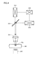
- a laser annealing device used for activating an ion implanted impurity is described.
- This device includes first and second lasers 201 and 202, a trigger unit 200, a half mirror 203, a condenser lens 204, and a heater 205.
- a dichroic mirror may be used instead of the half mirror.
- Trigger unit 200 transmits a trigger signal to first and second lasers 201 and 202 at the same time or at different timings.
- first and second lasers 201 and 202 emit pulse laser lights having first and second wavelengths, respectively.
- Half mirror 203 is arranged such that both of the laser lights from first and second lasers 201 and 202 enter condenser lens 204 along an optical axis.
- Condenser lens 204 condenses the laser lights from first and second lasers 201 and 202 onto an annealed region RG of work WK.
- Annealed region RG is laser annealed with the condensed laser light.
- Heater 205 heats work WK to assist the laser annealing.
- Wavelengths X and Y (meter) of the laser lights generated by first and second lasers 201 and 202, respectively, are selected to satisfy the following equation, provided that an extinction coefficient of silicon carbide with respect to light having a wavelength W (meter) is represented as k (W): k Y / Y ⁇ 5 ⁇ 10 5 ⁇ k X / X
- the laser light from first laser 201 tends to be absorbed near a surface of work WK compared to the laser light from second laser 202.
- the laser light from second laser 202 tends to reach a deeper position in work WK than the laser light from first laser 201.
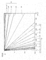
- Fig. 5 is a graph illustrating variation in light intensity RT when lights having wavelengths L1 to L36 reach a depth DP in silicon carbide.
- Wavelengths L1 to L21 are classified as a first group G1, and wavelengths L22 to L36 are classified as a second group G2.
- the wavelengths belonging to first group G1 correspond to first laser 201, and the wavelengths belonging to second group G2 correspond to second laser 202.
- wavelengths L1 to L13 are represented as a single hatching area instead of graphs. The same applies to wavelengths L25 to L36.
- a method of manufacturing semiconductor device 100 will now be described.
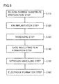
- a substrate preparation step (step S110: Fig. 6 ) is performed to prepare a silicon carbide substrate as follows.
- buffer layer 121 is formed on base substrate 80.
- base substrate 80 is of n conductivity type.
- Buffer layer 121 is made of silicon carbide of n conductivity type, and is an epitaxial layer having a thickness of 0.5 ⁇ m, for example.
- Buffer layer 121 has a conduction impurity concentration of 5 ⁇ 10 17 cm -3 , for example.
- n - layer 122 is formed on buffer layer 121. Specifically, a layer made of silicon carbide of n conductivity type is formed by epitaxial growth. N- layer 122 has a thickness of 10 ⁇ m, for example. N - layer 122 has an n conductivity type impurity concentration of 5 ⁇ 10 15 cm -3 , for example.
- the silicon carbide substrate including base substrate 80, buffer layer 121 and n - layer 122 ( Fig. 7 ) is prepared.
- This silicon carbide substrate has a surface made of n - layer 122 (upper surface in Fig. 7 ) and a rear surface made of base substrate 80 (lower surface in Fig. 7 ).
- an ion implantation step (step S120: Fig. 6 ) is performed to form the impurity regions (p B region 123, n + region 124 and p + region 125) by implanting ions from the surface of the silicon carbide substrate into the silicon carbide substrate.
- the impurity regions are formed as follows.
- a p conductivity type impurity is selectively implanted into a portion of n - layer 122, to form p B region 123. Then, an n conductivity type impurity is selectively implanted into a prescribed region to form n + region 124, and a p conductivity type impurity is selectively implanted into a prescribed region to form p + region 125.
- the selective implantations of the impurities are performed using a mask formed of an oxide film, for example.
- an annealing step for activating the implanted impurities is performed using the laser annealing device shown in Fig. 4 . That is, laser light having a wavelength selected from first group G 1 ( Fig. 5 ) (first laser light) and laser light having a wavelength selected from second group G2 ( Fig. 5 ) (second laser light) are applied to the surface of the silicon carbide substrate.
- the step of applying the first laser light is a step of applying the first laser light only to a first region which is a portion of the surface of the silicon carbide substrate.
- the first region includes at least n + region 124 and p + region 125.
- the step of applying the second laser light is a step of applying the second laser light to a second region which is a portion of the surface of the silicon carbide substrate.
- the second region includes at least p B region 123. More preferably, the first region is smaller than the second region.
- the steps of applying the first and second laser lights may be performed successively or simultaneously. It is preferable to raise the temperature of the silicon carbide substrate by heater 205 ( Fig. 4 ) before the first and second laser lights enter the substrate. It is preferable to apply the first and second laser lights either in an inert gas atmosphere, or in an atmosphere under a reduced pressure from atmospheric pressure. It is preferable that photon energy of each of the first and second laser lights be higher than band gap energy of the silicon carbide substrate.
- a gate insulating film formation step (step S 140: Fig. 6 ) is performed. Specifically, oxide film 126 is formed to cover n - layer 122, p B regions 123, n + regions 124, and p + regions 125. This formation may be done with dry oxidation (thermal oxidation). The dry oxidation is performed under the condition of a heating temperature of 1200°C and a heating period of 30 minutes, for example.
- a nitrogen annealing step (step S 150: Fig. 6 ) is performed. Specifically, an annealing process is performed in a nitrogen monoxide (NO) atmosphere. This process is performed under the condition of a heating temperature of 1100°C and a heating period of 120 minutes, for example. As a result, nitrogen atoms are introduced into a portion near an interface between each of n - layer 122, p B regions 123, n + regions 124, p + regions 125, and oxide film 126.
- NO nitrogen monoxide
- an annealing process using an argon (Ar) gas which is inert gas may be further performed. This process is performed under the condition of a heating temperature of 1100°C and a heating period of 60 minutes, for example.
- an electrode formation step (step S160: Fig. 6 ) is performed to form source electrode 111 and drain electrode 112 as follows.
- a resist film having a pattern is formed on oxide film 126 by photolithography. Using this resist film as a mask, a portion of oxide film 126 located on n + region 124 and p + region 125 is removed by etching. An opening is thus formed in oxide film 126. Then, a conductor film is formed to be in contact with n + region 124 and p + region 125 in this opening. The resist film is then removed to remove (lift off) a portion of the conductor film that has been located on the resist film.
- This conductor film may be a metal film, and is made of nickel (Ni), for example. As a result of this liftoff, source electrode 111 is formed.
- heat treatment is performed for two minutes in an atmosphere of an argon (Ar) gas which is inert gas at a heating temperature of 950°C.
- upper source electrode 127 is formed on source electrode 111.
- Drain electrode 112 is formed on the rear surface of base substrate 80.
- Gate electrode 110 is formed on oxide film 126. Consequently, semiconductor device 100 is obtained.
- the annealing is performed by combination of the laser light of first group G1 ( Fig. 5 ) that tends to be absorbed particularly near the surface of the silicon carbide substrate, and the laser light of second group G2 ( Fig. 5 ) that tends to reach a deep position from the surface of the silicon carbide substrate.
- the annealing conditions can be adjusted such that a portion near the surface is not annealed more strongly than necessary, while a region deep in the silicon carbide substrate is sufficiently annealed.
- damage to the surface of the silicon carbide substrate can be reduced.
- the above function and effect is particularly useful in a structure having a diffusion region of relatively low concentration such as p B region 123 and a diffusion region of relatively high concentration such as n + region 124 and p + region 125 at a surface side of the low concentration diffusion region, i.e., a structure having double diffusion.
- laser light of first group G1 that tends to be absorbed in a shallower position than laser light of second group G2 contributes mainly to the annealing of n + region 124 and p + region 125 located in a shallower position than p B region 123. Consequently, the laser light of second group G2 can be optimized to anneal mainly p B region 123.
- P B region 123 is sufficiently activated by relatively weak annealing due to its impurity concentration lower than those of n + region 124 and p + region 125.
- the intensity of the laser light of second group G2 can be made lower than when the laser light of first group G1 is not used together.
- damage to the surface of the silicon carbide substrate can be reduced.
- the laser light of first group G1 is applied only to a partial region of the surface of silicon carbide, damage to the other region and warp of the substrate can be suppressed. Furthermore, since the region irradiated with the laser light of first group G1 is smaller than the region irradiated with the laser light of second group G2, a portion of the surface irradiated with both laser lights, i.e., a portion that tends to be more significantly damaged can be made smaller than when both regions have the same size. In particular, damage to a portion of the surface of the silicon carbide substrate opposite gate electrode 110 ( Fig. 1 ) can be suppressed, to improve reliability of semiconductor device 100. This is because surface roughness due to the damage of this portion results in lowered reliability of the gate insulating film (oxide film 126) formed on this portion, facilitating the generation of leak current.
- the laser lights of first group G1 and second group G2 may be successively applied.
- the application steps can be controlled independently of each other.
- the laser lights may be simultaneously applied.
- the silicon carbide substrate is heated to a higher temperature than when the lights are applied separately. Thus, stronger annealing can be performed.
- heater 205 ( Fig. 4 ) is used, the intensity of laser light required for sufficient annealing can be reduced.
- the annealing is performed either in an inert gas atmosphere, or in an atmosphere under a reduced pressure from atmospheric pressure, deterioration of the surface of the silicon carbide substrate can be suppressed.
- photon energy of laser light used for the laser annealing is higher than band gap energy of the silicon carbide substrate, the laser light can be absorbed in the silicon carbide substrate with greater efficiency.
- a vertical DiMOSFET has been illustrated, another semiconductor device such as a RESURF-JFET (Reduced Surface Field-Junction Field Effect Transistor) or a Schottky diode may be manufactured using the semiconductor substrate of the present invention.
- RESURF-JFET Reduced Surface Field-Junction Field Effect Transistor
- Schottky diode may be manufactured using the semiconductor substrate of the present invention.
- 100 semiconductor device 110 gate electrode; 111 source electrode; 112 drain electrode; 121 buffer layer; 122 n - layer; 123 p B region; 124 n + region; 125 p + region; 126 oxide film; 127 upper source electrode, 200 trigger unit; 201 first laser; 202 second laser; 203 half mirror; 204 condenser lens; 205 heater.
Landscapes
- Physics & Mathematics (AREA)
- Engineering & Computer Science (AREA)
- Computer Hardware Design (AREA)
- Microelectronics & Electronic Packaging (AREA)
- Power Engineering (AREA)
- Condensed Matter Physics & Semiconductors (AREA)
- General Physics & Mathematics (AREA)
- Manufacturing & Machinery (AREA)
- High Energy & Nuclear Physics (AREA)
- Toxicology (AREA)
- Health & Medical Sciences (AREA)
- Chemical & Material Sciences (AREA)
- Crystallography & Structural Chemistry (AREA)
- Electromagnetism (AREA)
- Optics & Photonics (AREA)
- Electrodes Of Semiconductors (AREA)
- Insulated Gate Type Field-Effect Transistor (AREA)
Applications Claiming Priority (2)
| Application Number | Priority Date | Filing Date | Title |
|---|---|---|---|
| JP2010272622A JP5569376B2 (ja) | 2010-12-07 | 2010-12-07 | 半導体装置の製造方法 |
| PCT/JP2011/075590 WO2012077443A1 (ja) | 2010-12-07 | 2011-11-07 | 半導体装置の製造方法 |
Publications (1)
| Publication Number | Publication Date |
|---|---|
| EP2650909A1 true EP2650909A1 (en) | 2013-10-16 |
Family
ID=46206945
Family Applications (1)
| Application Number | Title | Priority Date | Filing Date |
|---|---|---|---|
| EP11846625.9A Withdrawn EP2650909A1 (en) | 2010-12-07 | 2011-11-07 | Method for manufacturing semiconductor device |
Country Status (8)
Families Citing this family (7)
| Publication number | Priority date | Publication date | Assignee | Title |
|---|---|---|---|---|
| CA2772610C (en) | 2009-08-28 | 2018-01-23 | The Cleveland Clinic Foundation | Sdf-1 delivery for treating ischemic tissue |
| JP5694096B2 (ja) * | 2011-09-08 | 2015-04-01 | 株式会社東芝 | 炭化珪素半導体装置の製造方法 |
| US9966339B2 (en) | 2014-03-14 | 2018-05-08 | Taiwan Semiconductor Manufacturing Company | Barrier structure for copper interconnect |
| US8962468B1 (en) | 2014-04-23 | 2015-02-24 | United Silicon Carbide, Inc. | Formation of ohmic contacts on wide band gap semiconductors |
| CN106471605A (zh) * | 2014-04-23 | 2017-03-01 | 美国联合碳化硅公司 | 宽带隙半导体上的欧姆触点的形成 |
| JP6870286B2 (ja) * | 2016-11-15 | 2021-05-12 | 富士電機株式会社 | 炭化珪素半導体装置の製造方法 |
| CN113097059A (zh) * | 2021-04-07 | 2021-07-09 | 芯璨半导体科技(山东)有限公司 | 一种铝掺杂4h碳化硅的激光热处理方法 |
Family Cites Families (10)
| Publication number | Priority date | Publication date | Assignee | Title |
|---|---|---|---|---|
| JPS56142630A (en) * | 1980-04-09 | 1981-11-07 | Fujitsu Ltd | Manufacture of semiconductor device |
| EP0971397B1 (en) * | 1997-11-28 | 2003-04-23 | Matsushita Electric Industrial Co., Ltd. | Method and device for activating semiconductor impurities |
| JP2000340671A (ja) * | 1999-05-26 | 2000-12-08 | Fujitsu Ltd | 半導体装置の製造方法及び半導体装置 |
| JP3820424B2 (ja) * | 2001-03-27 | 2006-09-13 | 独立行政法人産業技術総合研究所 | 不純物イオン注入層の活性化法 |
| US7109087B2 (en) * | 2003-10-03 | 2006-09-19 | Applied Materials, Inc. | Absorber layer for DSA processing |
| JP2005302883A (ja) * | 2004-04-08 | 2005-10-27 | Hitachi Ltd | 半導体装置の製造方法 |
| JP2006351659A (ja) * | 2005-06-14 | 2006-12-28 | Toyota Motor Corp | 半導体装置の製造方法 |
| US7928469B2 (en) * | 2005-10-19 | 2011-04-19 | Mitsubishi Electric Corporation | MOSFET and method for manufacturing MOSFET |
| JP2007123300A (ja) * | 2005-10-25 | 2007-05-17 | Toyota Motor Corp | 不純物活性化方法、レーザアニール装置、半導体装置とその製造方法 |
| DE102008003953A1 (de) * | 2007-02-28 | 2008-09-04 | Fuji Electric Device Technology Co. Ltd. | Verfahren zur Herstellung eines Halbleiterelements |
-
2010
- 2010-12-07 JP JP2010272622A patent/JP5569376B2/ja not_active Expired - Fee Related
-
2011
- 2011-11-07 US US13/583,564 patent/US8609521B2/en active Active
- 2011-11-07 CA CA2792550A patent/CA2792550A1/en not_active Abandoned
- 2011-11-07 CN CN2011800188617A patent/CN102859660A/zh active Pending
- 2011-11-07 KR KR1020127024090A patent/KR20130135725A/ko not_active Withdrawn
- 2011-11-07 EP EP11846625.9A patent/EP2650909A1/en not_active Withdrawn
- 2011-11-07 WO PCT/JP2011/075590 patent/WO2012077443A1/ja active Application Filing
- 2011-11-15 TW TW100141705A patent/TW201225162A/zh unknown
Non-Patent Citations (1)
| Title |
|---|
| See references of WO2012077443A1 * |
Also Published As
| Publication number | Publication date |
|---|---|
| JP5569376B2 (ja) | 2014-08-13 |
| WO2012077443A9 (ja) | 2012-11-08 |
| US20130040445A1 (en) | 2013-02-14 |
| WO2012077443A1 (ja) | 2012-06-14 |
| CA2792550A1 (en) | 2012-06-14 |
| US8609521B2 (en) | 2013-12-17 |
| CN102859660A (zh) | 2013-01-02 |
| TW201225162A (en) | 2012-06-16 |
| JP2012124263A (ja) | 2012-06-28 |
| KR20130135725A (ko) | 2013-12-11 |
Similar Documents
| Publication | Publication Date | Title |
|---|---|---|
| EP2650909A1 (en) | Method for manufacturing semiconductor device | |
| JP7229852B2 (ja) | 炭化ケイ素ウェハを処理するための方法および炭化ケイ素半導体デバイス | |
| US9892919B2 (en) | Semiconductor device manufacturing method | |
| US8252672B2 (en) | Silicon carbide semiconductor device comprising silicon carbide layer and method of manufacturing the same | |
| CN102479807B (zh) | 碳化硅半导体装置及其制造方法 | |
| CN215183858U (zh) | 电子器件 | |
| US10453687B2 (en) | Method of manufacturing semiconductor device | |
| JP6647621B2 (ja) | 不純物導入装置、不純物導入方法及び半導体素子の製造方法 | |
| EP2015348A2 (en) | Method for manufacturing a SiC semiconductor device | |
| JP4506100B2 (ja) | 炭化珪素ショットキーバリアダイオードの製造方法 | |
| JP4862207B2 (ja) | 半導体装置の製造方法 | |
| JP6870286B2 (ja) | 炭化珪素半導体装置の製造方法 | |
| JP4827829B2 (ja) | 炭化珪素半導体基板の製造方法および炭化珪素半導体装置の製造方法 | |
| JP2010073857A (ja) | 半導体装置の製造方法 | |
| JP2024528579A (ja) | 電子半導体部品の製造方法 | |
| JP2005223219A (ja) | 薄膜及びp型酸化亜鉛薄膜製造方法と半導体デバイス | |
| JP4250822B2 (ja) | 炭化珪素半導体装置の製造方法 | |
| JP6387855B2 (ja) | 炭化珪素半導体装置の製造方法およびそれに用いるレーザ加工装置 | |
| JP5092353B2 (ja) | 炭化珪素へのドーピング方法および炭化珪素半導体装置の製造方法 | |
| US20130109200A1 (en) | Method for manufacturing semiconductor device | |
| EP4420153B1 (en) | Coating-assisted laser annealing process for the manufacturing of wide-bandgap semiconductor devices | |
| US7195996B2 (en) | Method of manufacturing silicon carbide semiconductor device | |
| KR20040046644A (ko) | 레이저 활성화를 이용한 화합물 반도체 소자의 제조방법 | |
| KR20250112833A (ko) | 반도체 기판 및 반도체 기판의 제조 방법 | |
| JP2005294732A (ja) | 導電特性領域の作成方法 |
Legal Events
| Date | Code | Title | Description |
|---|---|---|---|
| PUAI | Public reference made under article 153(3) epc to a published international application that has entered the european phase |
Free format text: ORIGINAL CODE: 0009012 |
|
| 17P | Request for examination filed |
Effective date: 20130225 |
|
| AK | Designated contracting states |
Kind code of ref document: A1 Designated state(s): AL AT BE BG CH CY CZ DE DK EE ES FI FR GB GR HR HU IE IS IT LI LT LU LV MC MK MT NL NO PL PT RO RS SE SI SK SM TR |
|
| DAX | Request for extension of the european patent (deleted) | ||
| STAA | Information on the status of an ep patent application or granted ep patent |
Free format text: STATUS: THE APPLICATION HAS BEEN WITHDRAWN |
|
| 18W | Application withdrawn |
Effective date: 20141024 |