EP2618128A1 - Dispositif de détection, détecteur et appareil d'imagerie l'utilisant - Google Patents
Dispositif de détection, détecteur et appareil d'imagerie l'utilisant Download PDFInfo
- Publication number
- EP2618128A1 EP2618128A1 EP13151169.3A EP13151169A EP2618128A1 EP 2618128 A1 EP2618128 A1 EP 2618128A1 EP 13151169 A EP13151169 A EP 13151169A EP 2618128 A1 EP2618128 A1 EP 2618128A1
- Authority
- EP
- European Patent Office
- Prior art keywords
- detecting device
- antenna
- electromagnetic waves
- semiconductor rectifying
- rectifying devices
- Prior art date
- Legal status (The legal status is an assumption and is not a legal conclusion. Google has not performed a legal analysis and makes no representation as to the accuracy of the status listed.)
- Withdrawn
Links
- 238000003384 imaging method Methods 0.000 title claims description 13
- 239000004065 semiconductor Substances 0.000 claims abstract description 144
- 230000000644 propagated effect Effects 0.000 claims abstract description 27
- 239000004020 conductor Substances 0.000 claims description 42
- 238000005259 measurement Methods 0.000 claims description 12
- 230000005540 biological transmission Effects 0.000 claims description 8
- 230000005684 electric field Effects 0.000 claims description 7
- 230000004888 barrier function Effects 0.000 description 50
- 238000010586 diagram Methods 0.000 description 37
- 239000000463 material Substances 0.000 description 8
- 238000000034 method Methods 0.000 description 7
- 230000035945 sensitivity Effects 0.000 description 7
- 239000000758 substrate Substances 0.000 description 5
- VYPSYNLAJGMNEJ-UHFFFAOYSA-N Silicium dioxide Chemical compound O=[Si]=O VYPSYNLAJGMNEJ-UHFFFAOYSA-N 0.000 description 4
- 230000000052 comparative effect Effects 0.000 description 4
- 229910001218 Gallium arsenide Inorganic materials 0.000 description 3
- 238000001816 cooling Methods 0.000 description 3
- 230000003247 decreasing effect Effects 0.000 description 3
- 239000007772 electrode material Substances 0.000 description 3
- 230000000704 physical effect Effects 0.000 description 3
- 230000009467 reduction Effects 0.000 description 3
- 230000004044 response Effects 0.000 description 3
- 238000004088 simulation Methods 0.000 description 3
- 238000004364 calculation method Methods 0.000 description 2
- 229910052681 coesite Inorganic materials 0.000 description 2
- 229910052906 cristobalite Inorganic materials 0.000 description 2
- 238000001514 detection method Methods 0.000 description 2
- 238000009826 distribution Methods 0.000 description 2
- 150000002500 ions Chemical class 0.000 description 2
- 238000004519 manufacturing process Methods 0.000 description 2
- 230000004048 modification Effects 0.000 description 2
- 238000012986 modification Methods 0.000 description 2
- 230000000737 periodic effect Effects 0.000 description 2
- 239000005360 phosphosilicate glass Substances 0.000 description 2
- 230000008569 process Effects 0.000 description 2
- 230000001902 propagating effect Effects 0.000 description 2
- 239000000377 silicon dioxide Substances 0.000 description 2
- 229910052682 stishovite Inorganic materials 0.000 description 2
- 229910052905 tridymite Inorganic materials 0.000 description 2
- 229910012463 LiTaO3 Inorganic materials 0.000 description 1
- 238000000862 absorption spectrum Methods 0.000 description 1
- 229910021417 amorphous silicon Inorganic materials 0.000 description 1
- 230000008901 benefit Effects 0.000 description 1
- 239000003990 capacitor Substances 0.000 description 1
- 238000004891 communication Methods 0.000 description 1
- 150000001875 compounds Chemical class 0.000 description 1
- 238000011109 contamination Methods 0.000 description 1
- 230000007423 decrease Effects 0.000 description 1
- 230000001419 dependent effect Effects 0.000 description 1
- 238000000151 deposition Methods 0.000 description 1
- 238000001312 dry etching Methods 0.000 description 1
- 230000000694 effects Effects 0.000 description 1
- 238000005530 etching Methods 0.000 description 1
- 230000005669 field effect Effects 0.000 description 1
- 239000002184 metal Substances 0.000 description 1
- 229910052751 metal Inorganic materials 0.000 description 1
- 150000004767 nitrides Chemical class 0.000 description 1
- 229910052763 palladium Inorganic materials 0.000 description 1
- 238000002161 passivation Methods 0.000 description 1
- 238000000206 photolithography Methods 0.000 description 1
- 229910052697 platinum Inorganic materials 0.000 description 1
- 230000010287 polarization Effects 0.000 description 1
- 229910052710 silicon Inorganic materials 0.000 description 1
- 239000010703 silicon Substances 0.000 description 1
- 238000003325 tomography Methods 0.000 description 1
- XLYOFNOQVPJJNP-UHFFFAOYSA-N water Substances O XLYOFNOQVPJJNP-UHFFFAOYSA-N 0.000 description 1
- 238000001039 wet etching Methods 0.000 description 1
Images


Classifications
-
- H—ELECTRICITY
- H01—ELECTRIC ELEMENTS
- H01L—SEMICONDUCTOR DEVICES NOT COVERED BY CLASS H10
- H01L27/00—Devices consisting of a plurality of semiconductor or other solid-state components formed in or on a common substrate
- H01L27/14—Devices consisting of a plurality of semiconductor or other solid-state components formed in or on a common substrate including semiconductor components sensitive to infrared radiation, light, electromagnetic radiation of shorter wavelength or corpuscular radiation and specially adapted either for the conversion of the energy of such radiation into electrical energy or for the control of electrical energy by such radiation
- H01L27/144—Devices controlled by radiation
- H01L27/146—Imager structures
- H01L27/14665—Imagers using a photoconductor layer
- H01L27/14669—Infrared imagers
-
- G—PHYSICS
- G01—MEASURING; TESTING
- G01N—INVESTIGATING OR ANALYSING MATERIALS BY DETERMINING THEIR CHEMICAL OR PHYSICAL PROPERTIES
- G01N21/00—Investigating or analysing materials by the use of optical means, i.e. using sub-millimetre waves, infrared, visible or ultraviolet light
- G01N21/17—Systems in which incident light is modified in accordance with the properties of the material investigated
- G01N21/25—Colour; Spectral properties, i.e. comparison of effect of material on the light at two or more different wavelengths or wavelength bands
- G01N21/31—Investigating relative effect of material at wavelengths characteristic of specific elements or molecules, e.g. atomic absorption spectrometry
- G01N21/35—Investigating relative effect of material at wavelengths characteristic of specific elements or molecules, e.g. atomic absorption spectrometry using infrared light
- G01N21/3581—Investigating relative effect of material at wavelengths characteristic of specific elements or molecules, e.g. atomic absorption spectrometry using infrared light using far infrared light; using Terahertz radiation
-
- G—PHYSICS
- G01—MEASURING; TESTING
- G01S—RADIO DIRECTION-FINDING; RADIO NAVIGATION; DETERMINING DISTANCE OR VELOCITY BY USE OF RADIO WAVES; LOCATING OR PRESENCE-DETECTING BY USE OF THE REFLECTION OR RERADIATION OF RADIO WAVES; ANALOGOUS ARRANGEMENTS USING OTHER WAVES
- G01S7/00—Details of systems according to groups G01S13/00, G01S15/00, G01S17/00
- G01S7/02—Details of systems according to groups G01S13/00, G01S15/00, G01S17/00 of systems according to group G01S13/00
- G01S7/03—Details of HF subsystems specially adapted therefor, e.g. common to transmitter and receiver
- G01S7/032—Constructional details for solid-state radar subsystems
-
- G—PHYSICS
- G01—MEASURING; TESTING
- G01S—RADIO DIRECTION-FINDING; RADIO NAVIGATION; DETERMINING DISTANCE OR VELOCITY BY USE OF RADIO WAVES; LOCATING OR PRESENCE-DETECTING BY USE OF THE REFLECTION OR RERADIATION OF RADIO WAVES; ANALOGOUS ARRANGEMENTS USING OTHER WAVES
- G01S13/00—Systems using the reflection or reradiation of radio waves, e.g. radar systems; Analogous systems using reflection or reradiation of waves whose nature or wavelength is irrelevant or unspecified
- G01S13/003—Bistatic radar systems; Multistatic radar systems
-
- G—PHYSICS
- G01—MEASURING; TESTING
- G01S—RADIO DIRECTION-FINDING; RADIO NAVIGATION; DETERMINING DISTANCE OR VELOCITY BY USE OF RADIO WAVES; LOCATING OR PRESENCE-DETECTING BY USE OF THE REFLECTION OR RERADIATION OF RADIO WAVES; ANALOGOUS ARRANGEMENTS USING OTHER WAVES
- G01S13/00—Systems using the reflection or reradiation of radio waves, e.g. radar systems; Analogous systems using reflection or reradiation of waves whose nature or wavelength is irrelevant or unspecified
- G01S13/02—Systems using reflection of radio waves, e.g. primary radar systems; Analogous systems
- G01S13/0209—Systems with very large relative bandwidth, i.e. larger than 10 %, e.g. baseband, pulse, carrier-free, ultrawideband
-
- G—PHYSICS
- G01—MEASURING; TESTING
- G01S—RADIO DIRECTION-FINDING; RADIO NAVIGATION; DETERMINING DISTANCE OR VELOCITY BY USE OF RADIO WAVES; LOCATING OR PRESENCE-DETECTING BY USE OF THE REFLECTION OR RERADIATION OF RADIO WAVES; ANALOGOUS ARRANGEMENTS USING OTHER WAVES
- G01S7/00—Details of systems according to groups G01S13/00, G01S15/00, G01S17/00
- G01S7/02—Details of systems according to groups G01S13/00, G01S15/00, G01S17/00 of systems according to group G01S13/00
- G01S7/024—Details of systems according to groups G01S13/00, G01S15/00, G01S17/00 of systems according to group G01S13/00 using polarisation effects
-
- H—ELECTRICITY
- H01—ELECTRIC ELEMENTS
- H01Q—ANTENNAS, i.e. RADIO AERIALS
- H01Q1/00—Details of, or arrangements associated with, antennas
- H01Q1/36—Structural form of radiating elements, e.g. cone, spiral, umbrella; Particular materials used therewith
Definitions
- the present invention relates to a detecting device that detects electromagnetic waves, a detector, and an imaging apparatus that uses the detecting device and detector.
- a thermal detecting device As a detecting device that detects electromagnetic waves from millimeter wavebands (30 GHz to 300 GHz) to Terahertz bands (300 GHz to 30 THz), a thermal detecting device or a quantum detecting device has been used.
- a thermal detecting device may be a microbolometer that uses material such as a-Si, VOx, or the like, a pyroelectric element that uses material such as LiTaO3, TGS, or the like, and a Golay cell, or the like.
- Such a thermal detecting device is a device that can convert electromagnetic wave energy into heat energy, and detect changes in thermoelectric power. While a thermal detecting device does not necessarily have to have cooling, heat exchange is used, so response is relatively slow.
- a quantum detecting device may be an intrinsic semiconductor device that uses a semiconductor having no accepter or donor doping (MCT, photoconductive device, etc.) or an extrinsic semiconductor device that uses a semiconductor to which an acceptor or donor has been added, or doped.
- MCT semiconductor having no accepter or donor doping
- extrinsic semiconductor device that uses a semiconductor to which an acceptor or donor has been added, or doped.
- Such a quantum detecting device is a device that captures the electromagnetic waves as photons, and detects the photovoltaic power or resistance changes from the semiconductor having a smaller band gap. While response is relatively fast, the heat energy from the ambient temperature cannot be ignored, and so cooling is needed.
- a detecting device that detects electromagnetic waves from millimeter wavebands to Terahertz bands, using an antenna and semiconductor rectifying device, has been used.
- This detecting device captures electromagnetic waves as a high frequency signal, rectifies the high frequency signal received by an antenna or the like with a semiconductor rectifying device such as a Schottky barrier diode or the like, and detects the current flow at that time.
- the function of an RC low-pass filter is formed of junction capacity Cj in the Schottky barrier and serial resistance Rs. That is to say, high frequency components of the signal are cut off by the function of the RC low-pass filter, which then cannot be detected by the detecting device. Therefore, the cutoff frequency serving as the upper limit of the frequency band beyond which the detecting device cannot detect has to be higher than the frequency band of the electromagnetic wave to be detected.
- fc becomes approximately 300 GHz. If the junction area of the Schottky electrode is microfabricated to 0.1 ⁇ m 2 which is one-tenth thereof (approximately 0.3 ⁇ m 2 by when converted into terms of diameter), then fc becomes approximately 3 THz. Further, if the junction area of the Schottky electrode is microfabricated to 0.01 ⁇ m 2 which is one-tenth thereof (approximately 0.1 ⁇ m 2 when converted into terms of diameter), then fc can be estimated to be approximately 30 THz.
- Japanese Patent Laid-Open No. 09-162424 discloses a detecting device that detects high frequency electromagnetic waves in this manner.
- the junction area of a Schottky barrier diode which is a semiconductor rectifying device is microfabricated to 0.0007 ⁇ m 2 , and an electromagnetic wave of approximately 28 THz from a CO 2 laser (wavelength 10.6 ⁇ m) is detected.
- the junction area of the semiconductor rectifying device has been microfabricated in order to increase the cutoff frequency which is the frequency at the upper limit of the frequency band that can be detected.
- the current flowing through the semiconductor rectifying device is limited, whereby the device resistance of the semiconductor rectifying device is increases.
- the device resistance results in at least several thousand ⁇ .
- the present invention provides a detecting device to detect electromagnetic waves with improved sensitivity, by reducing device resistance.
- the present invention in its first aspect provides a detecting device as specified in claims 1 to 13.
- the present invention in its second aspect provides a detector as specified in claim 14.
- the present invention in its second aspect provides an imaging apparatus as specified in claim 15.
- the device resistance of the overall detecting device is reduced, and accordingly electric power efficiency for detecting electromagnetic waves is increased, so the sensitivity of the detecting device is improved.
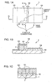
- Fig. 1A is a perspective diagram illustrating a schematic configuration of a detecting device according to a first embodiment.
- Fig. 1B is a diagram illustrating a cross-section of a detecting device according to the first embodiment.
- Fig. 1C is a diagram illustrating a cross-section of a detecting device that is parallel as to a plane of common phase of electromagnetic waves, according to the first embodiment.
- Fig. 2 is a diagram illustrating an equivalent circuit of a detecting device according to the first embodiment.
- Figs. 3A through 3F are diagrams illustrating the disposal of a semiconductor rectifying device according to the first embodiment.
- Fig. 4A is a diagram illustrating a configuration of a detecting device according to a second embodiment.
- Fig. 4B is a diagram illustrating a cross-section of a detecting device according to the second embodiment.
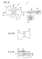
- Fig. 5A is a diagram illustrating a configuration of a detector according to a third embodiment.
- Fig. 5B is a diagram illustrating an enlarged view of the center portion of a detecting device according to the third embodiment.
- Fig. 5C is a diagram illustrating a cross-section of a detecting device according to the third embodiment.
- Fig. 6 is a diagram illustrating the impedance of an antenna according to the third embodiment.
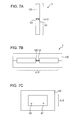
- Figs. 7A through 7C are diagrams illustrating modification examples of the antenna according to the third embodiment.
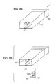
- Fig. 8A is a perspective diagram illustrating a schematic configuration of a detecting device according to a fourth embodiment.
- Fig. 8B is an exploded perspective diagram illustrating the detecting device and a semiconductor chip according to the fourth embodiment.
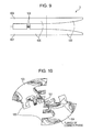
- Fig. 9 is a diagram illustrating a detecting device applied to a planar antenna according to the fourth embodiment.
- Fig. 10 is a diagram illustrating a phase of electromagnetic waves of the detecting device according to the third embodiment.
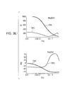
- Fig. 11 is a diagram comparing a comparative example with the present invention.
- Fig. 12 is a schematic diagram illustrating a schematic configuration of an imaging apparatus according to another embodiment.
- the detecting device relates to a detecting device that receives electromagnetic waves by a receiving antenna, and detects electromagnetic waves (oscillating electric field) that propagate over an antenna using a semiconductor rectifying device such as a Schottky barrier diode or the like.
- the device resistance of the device in a semiconductor rectifying device increases itself.
- the detecting device has an antenna that receives electromagnetic waves and multiple semiconductor rectifying devices, which are serially connected to the antenna and are connected so as to be mutually parallel with the polarity in the same direction, and which receive the electromagnetic waves propagated from the antenna.
- the multiple semiconductor rectifying devices are each disposed in positions so that the phase of the electromagnetic waves (oscillating electric field) that propagated from the antenna is substantially the same phase.
- disposing the semiconductor rectifying devices with the same phase means that the semiconductor rectifying devices are each disposed in positions so that the phases of the electromagnetic waves propagated from the antenna are substantially the same phase.
- the positions for each of the multiple semiconductor rectifying devices to be disposed are not limited to positions where the absolute value of the phase difference of the propagated electromagnetic wave is 0, and positions having a phase difference within a predetermined range is allowable.
- positions having a phase difference in propagated electromagnetic waves of 0 or greater and ⁇ /16 are included as the same phase. Details of the disposal of the semiconductor rectifying devices will be described later.
- a semiconductor rectifying device may be a Schottky barrier diode, planar doped barrier diode (PDBD), PN (PIN) diode, Mott diode, backward diode, self-switching diode, and the like. Also, the semiconductor rectifying device may be used as a base-emitter configuration in a transistor or a gate-source configuration in a field-effect transistor (FET).
- PDBD planar doped barrier diode
- PIN PIN
- Mott diode Mott diode
- backward diode backward diode
- self-switching diode and the like.
- the semiconductor rectifying device may be used as a base-emitter configuration in a transistor or a gate-source configuration in a field-effect transistor (FET).
- FET field-effect transistor
- the antenna may be a dipole antenna, slot antenna, patch antenna, Cassegrain antenna, parabola antenna or the like. Also, the antenna is not restricted to planar antennas, and a stereo antenna may be used.
- the detecting device according to a first embodiment will be described with reference to Fig. 1 . Configuration of Detecting Device
- Fig. 1A is a diagram illustrating a schematic configuration of a detecting device, where a portion is enlarged, according to the present embodiment.
- Fig. 1B is a diagram illustrating a cross-section of a detecting device according to the present embodiment, perpendicular as to planes of common phase of electromagnetic waves, taken along line IB in Fig. 1A.
- Fig. 1C is a diagram illustrating a cross-section of a detecting device according to the present embodiment, parallel as to planes of common phase of electromagnetic waves, taken along line IC in Fig. 1A .
- a detecting device 3 has two semiconductor rectifying devices 101, and strip conductors 103 and 104 which are conductors made up of A1 serving as antennas that propagate electromagnetic waves. Also, the detecting device 3 has a substrate 1, dielectric 2, and semiconductor layer 102. That is to say, at least one of the conductors making up the antenna and a semiconductor rectifying device are serially connected electrically via the semiconductor layer.
- Figs. 1A through 1C illustrate a contact portion, where the semiconductor rectifying devices 101 and strip conductors 103 and 104 are contact, in an enlarged manner.
- the detecting device 3 has two independent semiconductor rectifying devices 101, and are serially connected electrically so that the polarity of the strip conductors 103 and 104 which are antennas are facing the same direction. Also, the two semiconductor rectifying devices 101 are disposed so as to have the same phase as to the electromagnetic wave propagated from the strip conductors 103 and 104 which are antennas. This roughly equates to multiple semiconductor rectifying devices being disposed in positions where the phase of the electromagnetic wave propagated from the antenna is substantially the same phase.
- the semiconductor rectifying device 101 is in contact with the strip conductor 103 which is a portion of the antenna. That is to say, the antenna is made up of a pair of conductors, and multiple semiconductor rectifying devices are arrayed in parallel touching one conductor of the pair.
- the shape of the semiconductor rectifying device 101 according to the present embodiment is a uniform cylinder, and the periphery of the semiconductor rectifying device 101 is surrounded by a dielectric 2.
- the multiple semiconductor rectifying devices each have a cylindrical form where a junction making up the semiconductor rectifying device is surrounded by a dielectric.
- the multiple semiconductor rectifying devices are configured such that the areas of the cross-section perpendicular to the direction of current flowing at the junction making up the semiconductor rectifying devices are mutually equal.
- the dielectric 2 has a significantly higher resistance as to the propagated electromagnetic waves, as compared to the semiconductor rectifying device 101.
- the semiconductor device 101 is also in contact with the semiconductor layer 102.
- the two strip conductors 103 and 104 are in ohmic contact electrically via the semiconductor rectifying device 101 and semiconductor layer 102.
- the area of the junction of the semiconductor rectifying device 101 of the detecting device 3, in order to detect electromagnetic waves of a frequency band of 30 GHz to 30 THz, has a minute area that is 10 ⁇ m 2 or less.
- the area of the junction here is as described above.
- the junction of the strip conductor 103 and semiconductor device 101 can be considered to be junction area A. Also, if the semiconductor rectifying device uses PDBD or a transistor, the area indicates the junction area on a mesa.
- junction area A of the semiconductor rectifying device 1 ⁇ m 2 or less is preferable if the material of the semiconductor rectifying device uses silicon. Also, a junction area A of 10 ⁇ m 2 or less is preferable if, of compound semiconductor materials with a relatively high mobility, a Group III-V semiconductor material such as GaAs is used. This is because the junction capacity Cj of the semiconductor rectifying device 101 is determined from the typical junction thickness in a Schottky barrier diode being approximately 10 to 100 nm and the relative permittivity being approximately 10. Also, the serial resistance Rs of the semiconductor rectifying device 101 depends on the mobility of the material, but on minutely small areas as described above, reducing to around 100 ⁇ is difficult.
- the junction area of the semiconductor rectifying devices herein is near the precision limitation of photolithography such as a stepper or aligner. Therefore, a gap 105 that approximates the precision limitation in manufacturing occurs between the semiconductor rectifying device 101 and the strip conductor 104.
- the gap 105 is filled in with a semiconductor layer 102 having an electrical conductivity lower than the strip conductor 104, as needed, between the semiconductor rectifying device 101 and strip conductor 104.
- the semiconductor rectifying device 101 and strip conductor 104 are in ohmic contact electrically via the semiconductor layer 102.
- the main factor of the serial resistor Rs which is the resistance component from the semiconductor rectifying device 101 to the strip conductor 104 is the resistance of the semiconductor layer 102.
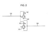
- the equivalent circuit of the detecting device 3 in the configuration described above with reference to Fig. 1 will be described below, having the junction area at the Schottky junction between the semiconductor rectifying device 101 and strip conductor 103 as A.
- Fig. 2 is a diagram illustrating an equivalent circuit of a detecting device according to the present embodiment.
- the circuit is assumed to be configured only with a serial resistor Rs which is a resistor combining the semiconductor rectifying device 101 and semiconductor layer 102 or the like, and a junction capacity Cj of the semiconductor rectifying device. That is to say, this can be viewed as a resistor-capacitor circuit (RC circuit) made up of the junction capacity Cj of the Schottky barrier diode 101 and the serial resistor Rs, i.e. an RC low-pass filter.
- RC circuit resistor-capacitor circuit
- the serial resistor Rs between the Schottky barrier diode 101 and strip conductor 104 can be viewed as being approximately the same as the resistor of the semiconductor layer 102, and is inversely proportional to ⁇ A at the junction area A between the Schottky barrier diode 101 and strip conductor 103.
- the serial resistor Rs has to be reduced, and as a method thereto, increasing the junction area A of the semiconductor rectifying device 101 may be considered.
- the detecting device 3 has two mutually independent semiconductor rectifying devices 101 of the junction area A, whereby reduction of the frequency band can be suppressed and combined impedance of the detecting device can be reduced. That is to say, the detection sensitivity of detecting can be improved as compared to a detecting device used in the past that uses one semiconductor rectifying device 101. Further details will be described below.
- the detecting device 3 has two semiconductor rectifying devices 101, which are disposed so that the phases of the electromagnetic waves propagated (transmitted) to the semiconductor rectifying devices 101 are the same phase, and the two semiconductor rectifying devices 101 are serially connected electrically and the polarity thereof are facing the same direction as to the propagated electromagnetic waves.
- the two serial resistors Rs are also serially connected and distributed, whereby in the case of combining resistance for the overall detecting device, the resistance becomes Rs/2.
- the semiconductor rectifying devices 101 are disposed so as to have the polarity thereof face the same direction, whereby the overall junction area is 2A, and the overall junction capacity is 2Cj.
- the cutoff frequency of the detecting device 3 being reduced can be suppressed, and also the device resistance of the entire detecting device as to the detected electromagnetic wave (combined resistance) can be reduced by half.
- the device resistance of the entire detecting device mismatching of resistance with an antenna having a comparatively small resistance value can be reduced.
- the disposal of the two Schottky barrier diodes used as semiconductor rectifying devices 101 are set as "positions at the same phase" as to the propagated electromagnetic wave, but even if not in positions where the phase difference is strictly 0, the advantage of the present invention of improving detecting sensitivity can be obtained.
- a position at the same phase is not limited to disposal where the phase difference of electromagnetic waves propagated to each of multiple semiconductor rectifying devices is 0, and disposal having a phase difference within a predetermined range is allowable.
- a position at the same phase is the position where the phases of the electromagnetic waves propagated from the antenna are substantially the same phase.
- the semiconductor rectifying devices are each disposed at these positions.
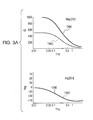
- FIG. 3 is a diagram describing the disposal relation of the two Schottky barrier diodes.
- the diagram illustrates the device resistance of the detecting device (combined resistance) [ ⁇ ], and a phase angle Mag[Zin] of the electromagnetic waves propagating over the two Schottky barrier diodes, as to the frequency bands of the detected electromagnetic waves.
- phase angles Arg[Zin] of the electromagnetic waves that are propagated over the two Schottky barrier diodes are separated.
- the phase angles Arg[Zin] gradually begin to match, and at ⁇ /64, are almost matched. Therefore, with a THz detector or the like for communication where phase angle becomes important, it is desirable for the disposal of the two semiconductor rectifying devices to be disposed so that the absolute value of the phase difference of the transmitted electromagnetic waves (oscillating electric field) is 0 or greater and ⁇ /32 or less.
- the impedance Mag[Zin] is half of when one Schottky barrier diode is used, and is roughly an ideal value. Therefore, in the case of using for an imaging apparatus or the like where phase angle does not have to be considered, it is more desirable for the two Schottky barrier diodes to be disposed so that the transmitted electromagnetic waves have a phase difference of 0 or greater and ⁇ /16 or less. That is to say, the combined impedance and the range of same phases from the perspective of a phase angle are determined according to the use situation of the detecting device.
- an optimal detecting wavelength is generally 32 to ( ⁇ /16)/2 ⁇ times the square root of the junction area thereof or more. Therefore, it is preferable for a detector according to the present embodiment to detect a frequency band from a millimeter waveband having a wavelength of 10 ⁇ m or greater to a terahertz band, where disposal of the Schottky barrier diodes are such that the phase difference is ⁇ /16 or less is easy.
- a portion of the strip conductor touching the Schottky barrier diodes 101 is flat so that the phase and wave front of the electromagnetic waves of the strip conductors 103 and 104 (e.g., equipotential plane) can be defined.
- Schottky barrier diodes having the same junction area A are used, but this is not restrictive, and Schottky barrier diodes each having different junction areas may also be used.
- configuring the detecting device using the same semiconductor rectifying devices is not restrictive, and semiconductor rectifying devices of different types or dimensions may be used.
- the present embodiment has n(n ⁇ 3) semiconductor rectifying devices such as Schottky barrier diodes or the like disposed in a row.
- the other configurations are the same as in the first embodiment, so descriptions of similar configurations will be omitted.
- FIG. 4A is a schematic diagram illustrating a detecting device according to the present embodiment.
- Fig. 4B is a diagram illustrating a cross-section of the detecting device that is vertical as to a plane of the same phase, according to the present embodiment.
- the present embodiment exemplifies a case of having three semiconductor rectifying devices 101, but is not limited to three. There may be three semiconductor rectifying devices 101, or the number may be expanded to 4, 5, ... n. That is to say, the detecting device according to the present embodiment only has to have multiple semiconductor rectifying devices, and these may be disposed so that at least three of the semiconductor rectifying devices have the same phase as to the electromagnetic wave. Now, when having n semiconductor rectifying devices, the detecting device resistance is ideally 1/n times the resistance of when there is one semiconductor rectifying device, which is low resistance.
- Parallelization efficiency here approximates to the amount of resistance that is decreased when n semiconductor rectifying devices are connected in parallel, and the ideal parallelization efficiency is approximately 1/n times as compared to when the combined resistance of the overall detecting device is one.
- a salient portion 106 may be provided to the strip conductor 104. That is to say, a salient portion 106 that is in a salient shape formed to be positioned between the semiconductor rectifying devices may be provided to the edge portion positioned on the semiconductor rectifying device side of the strip conductor 104. The reason thereof is to have the same shortest distance between the strip conductor 104 and all of the semiconductor rectifying devices 101, whereby the serial resistance Rs is not increased when the distance to the semiconductor layer 102 is short, and reduction of parallelization efficiency can be suppressed.
- the shape of the salient portion 106 is not limited to a rectangular shape, and various shapes such as a triangle, half-circle, or the like may be used. In the case that the number of devices of the semiconductor rectifying devices 101 increases to three or four, disposing the salient portion 106 of the strip conductor 104 formed of a material having an electric conductivity higher than the semiconductor layer 102 between the devices of the semiconductor rectifying devices 101 is effective.
- the salient portion 106 of the present embodiment is also important in an arrayed device array such that the phase difference between the semiconductor rectifying devices is sufficient small.
- the salient portions may be disposed in a mesh form.
- the configuration has multiple semiconductor rectifying devices connected to an antenna, but a configuration may have a transmission line that transmits electromagnetic waves connected to the antenna, enabling electromagnetic waves to be propagated to the semiconductor rectifying devices from the antenna via the transmission line.
- FIG. 5A is a perspective view of a detector according to the present embodiment.
- Fig. 5B is a diagram enlarging the center portion of the detector according to the present embodiment.
- Fig. 5C is a diagram illustrating a cross-section of the detector according to the present embodiment.
- the detector has a log periodic antenna serving as an antenna 100 that receives and transmits electromagnetic waves.
- the band received on the log periodic antenna is a wide band, and electromagnetic waves of various frequencies can be received on one antenna.
- the antenna 100 according to the present embodiment receives electromagnetic waves in frequency bands from 0.2 THz to 2.5 THz.
- the antenna 100 is made up of strip conductors 103 and 104, which are two non-contact conductors disposed on a substrate.
- the dimensions of the antenna 100 are 250 ⁇ m for the radius (outer radius) from the center portion where the illustrated Schottky barrier diode is disposed to the outermost side, 10 mm for the radius (inner radius) to the innermost side, the number of teeth having log period 0.7 is nine, and the angle of the teeth is 45 degrees.
- two mesa-shaped Schottky barrier diodes are disposed in the center portion of the strip conductors 103 and 104 so as to have a plane of common phase of the electromagnetic waves.
- the Schottky barrier diodes 101 are embedded in a oxide film or the like, and connected with the strip conductor 103 that approximates a Schottky electrode.
- the Schottky barrier diodes 101 are configured to be connected to the strip conductor 104 which approximates an ohmic electrode via the semiconductor layer 102 which is a high density carrier layer.
- the detecting device 3 with this type of configuration first forms a n+ layer with a carrier density of 10 19 cm -3 and a n layer of 10 18 cm -3 on an Si substrate with a Fz (Floating Zone) method, using an epitaxial growth method.
- etching is performed on an epitaxial layer, following which a Schottky electrode is formed on the epitaxial layer by vapor-depositing a Schottky metal, thereby forming a Schottky barrier diode 101. Both dry etching and wet etching may be used.
- the strip conductor 104 made up of A1 is formed, and passivation (Film protecting process to protect chip surface from contamination such as water, movable ions (ions that move freely and are not fixed) and increase device reliability.
- passivation Fin protecting process to protect chip surface from contamination such as water, movable ions (ions that move freely and are not fixed) and increase device reliability.
- Generally used materials are nitride film and phosphosilicate glass (PSG)) by a SiO 2 dielectric 2 is performed.
- the SiO 2 is exposed to expose the Schottky barrier diode 101.
- the strip conductor 103 made up of A1 is formed as a film, whereby the manufacturing of the detecting device according to the present embodiment is completed.
- the detecting device 3 according to the present embodiment can be readily manufactured using common semiconductor process techniques.
- the diameter on the contact portion side of the strip conductor 103 and Schottky barrier diode 101 is set to 0.6 ⁇ m and the distance between the Schottky barrier diode 101 and strip conductor 104 is 1 ⁇ m, so that the cutoff frequency of the RC low-pass filter is approximately 3 THz. Also, the spacing between the two Schottky barrier diodes 101 is 2 ⁇ m.
- Fig. 10 describes the results of simulating a plane of common phase of an antenna, whereby we can see that in the center area, wave fronts of electromagnetic waves that are approximately uniform with equal spacing (plane of common phase) are formed.
- the serial resistance Rs in the case of using one Schottky barrier diode according to the present embodiment is 1000 ⁇ . Therefore, the combined resistance of the detecting device according to the present embodiment where two Schottky barrier diodes 101 are connected in parallel is approximately 500 ⁇ .
- Ra is the resistance of the antenna
- Rd is the device resistance of the Schottky barrier diodes.
- Rd according to the present embodiment is the device resistance of the two Schottky barrier diodes.
- power efficiency can be found from the reflection coefficient herein, and the power efficiency can be found by 1 - ⁇ 2 . Therefore, from the above expression, power efficiency can be compared in the case of using one Schottky barrier diode and in the case of using two Schottky barrier diodes as with the present embodiment.
- Fig. 11 is a diagram comparing a configuration using one Schottky barrier diode with the present invention. The power efficiency increased from 28% in the case of one Schottky barrier diode to 48% in the present example.
- the cutoff frequency is 2 THz, both for the comparative example and the present invention. From this diagram, with the configuration of the present embodiment, the cutoff frequency is unchanged from the comparative example, but the power efficiency can be increased, i.e. the signal strength relating to electrical field strength of the electromagnetic wave (oscillating electrical field) obtained by the detector 4 can be increased, whereby SN (Signal/Noise) ratio can be increased compared to the comparative example.
- the detector 4 is connected to a mixer unit 202, high-frequency power source 201, and a current measurement unit (measuring unit) 203, via a read line 200.
- the electromagnetic wave (oscillating electrical field) received at the antenna 100 causes high-frequency current to flow at the detecting device 3.
- the high-frequency current is mixed with the high-frequency current applied from the high-frequency power source 201 at the mixer unit 202, and the mixed current is measured at the current measurement unit (measuring unit) 203.
- bias voltage may be applied to the read line 200 by an unshown voltage applying unit, thereby setting diode device operating point voltage.
- bias voltage is also dependent on the electrode material of the strip conductor 103 and so forth, so forward bias of around 0.1 V is optimal with electrode materials having a relatively low work function such as Ti and Al, and forward bias of around 0.3 to 0.5 V is optimal with electrode materials having a relatively low work function such as Pt and Pd.
- Fig. 6 is a diagram illustrating the results of impedance properties of the antenna 100, obtained by performing a simulation with a high-frequency total-field simulator HFSS v12 (manufactured by Ansoft).
- the antenna 100 according to the present embodiment is a self-complementary antenna, with impedance of 188 ⁇ . Further, effects of the permittivity ⁇ r of the Si substrate result in 188 ⁇ / ⁇ (1 + ⁇ r )/2 to 80 ⁇ , which is relatively low-impedance.
- FIGs. 7A through 7C are diagrams illustrating receiving antennas applicable to the present embodiment.
- log-periodic antennas and spiral antennas are effective with detecting devices capable of detecting electromagnetic waves with extremely broad frequency bands.
- Slot antennas and dipole antennas having resonant frequency properties are effective as detecting devices restricting frequency band of which reception is desired.
- the present embodiment is not restricted to dipole antennas, and resonant patch antennas and the like may be used as well.
- a feature of the detector according to the present embodiment is using a stereo antenna and a waveguide.
- Other configurations are the same as with the third embodiment, so description thereof will be omitted.
- Fig. 8A is a perspective view illustrating a detecting device according to the present embodiment.
- Fig. 8B is a diagram with the detecting device according to the present embodiment and semiconductor chip disassembled.
- a planar doped barrier diode 101 (hereinafter, PDBD) is used as a semiconductor rectifying device. Also, the arrangement includes a horn antenna 100 and a double-bridge waveguide 405 as a transmission line. Further, the detecting device 3 according to the present embodiment is arranged such that a semiconductor chip 41 includes a PDBD, so that the stereo antenna is mounted with a PDBD.
- the horn antenna 100 is advantageous in that it has excellent wideband properties, and also has good directivity.
- the double bridge waveguide 405 is used to guide the electromagnetic waves to the semiconductor chip.
- the traveling-wave antenna 100 according to the present embodiment is arranged to receive between 30 GHz to 0.1 THz.
- the double-bridge waveguide is 3.5 mm ⁇ 7.0 mm at the smallest portion, which is the near side in Figs. 8A and 8B , and each side is fourfold in length at the widest portion, which is the opening at the far side.
- Ridges 406 and 407 extend from the top and bottom directions in Figs. 8A and 8B , with the semiconductor chip 41 being soldered or the like to the ridges 406 and 407.
- Fig. 8B is a diagram illustrating the parts of the detecting device before mounting.
- a planar barrier is formed of an n-type layer / p-type layer / n-type layer of GaAs, on a GaAs substrate, having two mesas 101 which are 5 ⁇ m in diameter.
- Ohmic electrodes 403 and 404 which are the two electrodes of the PDBD are electrically connected to the ridges 406 and 407.
- the panes of electromagnetic waves from the traveling-wave antenna 100 temporally changes, but there is no phase difference between the two PDBDs, so the two PDBDs are located at the same phase.
- FIG. 9 is a diagram illustrating the configuration of a detecting device in a case of applying the configuration according to the present embodiment to a planar antenna.
- the detecting device 3 is of a configuration having a tapered slot antenna 100 and a slot line 405 (403, 404) serving as a transmission line.
- Fig. 12 is a diagram schematically illustrating the configuration of an imaging apparatus. As illustrated in Fig. 12 , the imaging apparatus 10 according to the present embodiment performs image pickup of images relating to objects of measurement.
- the imaging apparatus 10 includes an oscillator 11 emitting electromagnetic waves of a frequency band including a part of 30 GHz to 30 THz to an object of measurement, and an image pickup unit 12 which is an image constructing unit to construct an image of an object to be measured, where two of the detecting device 3 of the above embodiments are arrayed, so as to construct an image of the object of measurement based on information relating to electromagnetic waves which have transmitted and reflected off of the object of measurement, detected by the multiple detecting devices. Also included is a power source 13 to apply voltage to the oscillator 11.
- the imaging apparatus 10 emits terahertz waves generated at the oscillator 11 to the object of measurement, and detects transmitting waves and reflected waves thereafter at the detecting devices 3.
- physical property information such as absorption spectrum and refractive index of the object to be measured is obtained from signals relating to the field intensity (field distribution) of the terahertz waves detected at the detecting devices 3.
- constructing an image of the object of measurement from the obtained physical property information allows the physical property information of the object of measurement to be visualized.
- detecting devices with different antenna lengths may be disposed so as to realize an imaging apparatus corresponding to different frequencies. Also, arraying detecting devices with different antenna orientations also realizes imaging apparatus corresponding to different polarizations.
- the present invention may be applied to a conventionally-used tomography apparatus.
- a detecting device (3) to detect electromagnetic waves includes an antenna (100) configured to receive electromagnetic waves, and a plurality of semiconductor rectifying devices (101) serially connected to the antenna (100), and connected in parallel to each other such that the polarity is aligned, so as to receive electromagnetic waves propagated from the antenna (100), wherein the plurality of semiconductor rectifying devices (101) are each disposed at positions where the phase of electromagnetic waves propagated from the antenna (100) is substantially the same phase.
Applications Claiming Priority (1)
| Application Number | Priority Date | Filing Date | Title |
|---|---|---|---|
| JP2012009335 | 2012-01-19 |
Publications (1)
| Publication Number | Publication Date |
|---|---|
| EP2618128A1 true EP2618128A1 (fr) | 2013-07-24 |
Family
ID=47779825
Family Applications (1)
| Application Number | Title | Priority Date | Filing Date |
|---|---|---|---|
| EP13151169.3A Withdrawn EP2618128A1 (fr) | 2012-01-19 | 2013-01-14 | Dispositif de détection, détecteur et appareil d'imagerie l'utilisant |
Country Status (4)
| Country | Link |
|---|---|
| US (1) | US9437646B2 (fr) |
| EP (1) | EP2618128A1 (fr) |
| JP (1) | JP6141027B2 (fr) |
| CN (1) | CN103217587A (fr) |
Families Citing this family (6)
| Publication number | Priority date | Publication date | Assignee | Title |
|---|---|---|---|---|
| JP6296681B2 (ja) * | 2012-01-19 | 2018-03-20 | キヤノン株式会社 | 発振素子、発振器及びこれを用いた撮像装置 |
| JP6643799B2 (ja) * | 2014-11-28 | 2020-02-12 | キヤノン株式会社 | センサ、及び、これを用いた情報取得装置 |
| KR101804781B1 (ko) * | 2016-09-27 | 2018-01-10 | 현대자동차주식회사 | 영상 시스템 |
| US10332553B1 (en) | 2017-12-29 | 2019-06-25 | Headway Technologies, Inc. | Double ridge near-field transducers |
| KR20200014576A (ko) | 2018-08-01 | 2020-02-11 | 임철수 | 횡단보조 음성안내 보조장치 |
| CN110109082A (zh) * | 2019-04-17 | 2019-08-09 | 天津大学 | 一种共天线的太赫兹主动雷达成像阵列 |
Citations (6)
| Publication number | Priority date | Publication date | Assignee | Title |
|---|---|---|---|---|
| US5030962A (en) * | 1981-03-11 | 1991-07-09 | The Secretary Of State For Defence In Her Britannic Majesty's Government Of The United Kingdom Of Great Britain And Northern Ireland Of Whitehall | Electromagnetic radiation sensor |
| US5047783A (en) * | 1987-11-06 | 1991-09-10 | Millitech Corporation | Millimeter-wave imaging system |
| US5623145A (en) * | 1995-02-15 | 1997-04-22 | Lucent Technologies Inc. | Method and apparatus for terahertz imaging |
| JPH09162424A (ja) | 1995-12-04 | 1997-06-20 | Yokogawa Electric Corp | アンテナ結合電界検出型光検出素子およびその製造方法 |
| US20070001895A1 (en) * | 2003-08-12 | 2007-01-04 | Trex Enterprises | Multi-channel millimeter wave imaging system |
| US20080017813A1 (en) * | 2004-02-16 | 2008-01-24 | Jan Vetrovec | Composite dipole array systems and methods |
Family Cites Families (47)
| Publication number | Priority date | Publication date | Assignee | Title |
|---|---|---|---|---|
| US3671970A (en) * | 1970-08-31 | 1972-06-20 | Boeing Co | Switched rhombic automatic direction finding antenna system and apparatus |
| US3678414A (en) * | 1970-10-19 | 1972-07-18 | Collins Radio Co | Microstrip diode high isolation switch |
| US3852755A (en) * | 1971-07-22 | 1974-12-03 | Raytheon Co | Remotely powered transponder having a dipole antenna array |
| US4015259A (en) * | 1975-05-21 | 1977-03-29 | The United States Of America As Represented By The Secretary Of The Army | Method and apparatus for interrogating and identifying fixed or moving targets |
| FR2400781A1 (fr) * | 1977-06-24 | 1979-03-16 | Radant Etudes | Antenne hyperfrequence, plate, non dispersive, a balayage electronique |
| FR2412960A1 (fr) * | 1977-12-20 | 1979-07-20 | Radant Etudes | Dephaseur hyperfrequence et son application au balayage electronique |
| US4157550A (en) * | 1978-03-13 | 1979-06-05 | Alpha Industries, Inc. | Microwave detecting device with microstrip feed line |
| FR2448231A1 (fr) * | 1979-02-05 | 1980-08-29 | Radant Et | Filtre spatial adaptatif hyperfrequence |
| FR2469808A1 (fr) * | 1979-11-13 | 1981-05-22 | Etude Radiant Sarl | Dispositif de balayage electronique dans le plan de polarisation |
| US4302734A (en) * | 1980-03-12 | 1981-11-24 | Nasa | Microwave switching power divider |
| FR2506026A1 (fr) * | 1981-05-18 | 1982-11-19 | Radant Etudes | Procede et dispositif pour l'analyse d'un faisceau de rayonnement d'ondes electromagnetiques hyperfrequence |
| FR2514203B1 (fr) * | 1981-10-05 | 1986-04-25 | Radant Etudes | Filtre adaptatif spatial hyperfrequence pour antenne a polarisation quelconque et son procede de mise en oeuvre |
| US5574471A (en) * | 1982-09-07 | 1996-11-12 | Radant Systems, Inc. | Electromagnetic energy shield |
| US5621423A (en) * | 1983-08-29 | 1997-04-15 | Radant Systems, Inc. | Electromagnetic energy shield |
| FR2629920B1 (fr) * | 1984-01-23 | 1991-09-20 | Cmh Sarl | Filtre spatial adaptatif hyperfrequence fonctionnant a la reflexion et son procede de mise en oeuvre |
| US4542532A (en) * | 1984-03-09 | 1985-09-17 | Medtronic, Inc. | Dual-antenna transceiver |
| US5579024A (en) * | 1984-08-20 | 1996-11-26 | Radant Systems, Inc. | Electromagnetic energy shield |
| US5266963A (en) * | 1985-01-17 | 1993-11-30 | British Aerospace Public Limited Company | Integrated antenna/mixer for the microwave and millimetric wavebands |
| FR2595873B1 (fr) * | 1986-03-14 | 1988-09-16 | Thomson Csf | Reseau reflecteur a controle de phases et antenne comportant un tel reseau |
| FR2597621A1 (fr) * | 1986-04-22 | 1987-10-23 | Thomson Csf | Reseau d'elements diffusants d'energie electromagnetique a commande optique |
| US4910523A (en) * | 1987-11-06 | 1990-03-20 | Millitech Corporation | Micrometer wave imaging device |
| US4924238A (en) * | 1987-02-06 | 1990-05-08 | George Ploussios | Electronically tunable antenna |
| FR2614419B1 (fr) * | 1987-04-21 | 1989-06-16 | Centre Nat Rech Scient | Dispositif de mesure, en une pluralite de points, du champ micro-onde diffracte par un objet |
| US4806944A (en) * | 1987-09-14 | 1989-02-21 | General Electric Company | Switchable matching network for an element of a steerable antenna array |
| US5170140A (en) * | 1988-08-11 | 1992-12-08 | Hughes Aircraft Company | Diode patch phase shifter insertable into a waveguide |
| US4975712A (en) * | 1989-01-23 | 1990-12-04 | Trw Inc. | Two-dimensional scanning antenna |
| JPH02228072A (ja) * | 1989-03-01 | 1990-09-11 | Shindengen Electric Mfg Co Ltd | ショットキダイオード |
| CA2011298C (fr) * | 1990-03-01 | 1999-05-25 | Adrian William Alden | Antenne reseau de doublets a double polarisation |
| FR2663426B1 (fr) * | 1990-06-14 | 1992-10-02 | Centre Nat Rech Scient | Dispositif de mesure, en une pluralite de points d'une surface du champ micro-onde rayonne par une source. |
| CN2205014Y (zh) | 1994-09-26 | 1995-08-09 | 申漳 | 毫米波治疗仪的输出信号检测器 |
| JPH09197042A (ja) * | 1996-01-17 | 1997-07-31 | Eikichi Yamashita | ミリ波カメラ装置 |
| US6137996A (en) * | 1998-07-20 | 2000-10-24 | Motorola, Inc. | Apparatus and method for overcoming the effects of signal loss due to a multipath environment in a mobile wireless telephony system |
| US6317092B1 (en) * | 2000-01-31 | 2001-11-13 | Focus Antennas, Inc. | Artificial dielectric lens antenna |
| JP2001296183A (ja) * | 2000-04-17 | 2001-10-26 | Toyota Motor Corp | 赤外線検出装置並びに赤外線画像処理装置 |
| US7456803B1 (en) * | 2003-05-12 | 2008-11-25 | Hrl Laboratories, Llc | Large aperture rectenna based on planar lens structures |
| US7245269B2 (en) * | 2003-05-12 | 2007-07-17 | Hrl Laboratories, Llc | Adaptive beam forming antenna system using a tunable impedance surface |
| US7068234B2 (en) * | 2003-05-12 | 2006-06-27 | Hrl Laboratories, Llc | Meta-element antenna and array |
| US7105820B2 (en) * | 2004-01-16 | 2006-09-12 | New Jersey Institute Of Technology | Terahertz imaging for near field objects |
| US7358497B1 (en) * | 2005-04-08 | 2008-04-15 | University Of Central Florida Research Foundation, Inc. | Infrared/millimeter-wave focal plane array |
| US7324043B2 (en) * | 2005-09-02 | 2008-01-29 | Delphi Technologies, Inc. | Phase shifters deposited en masse for an electronically scanned antenna |
| FR2895574A1 (fr) * | 2005-12-22 | 2007-06-29 | France Telecom | Reflecteur bipolarisation configurable |
| US7605767B2 (en) * | 2006-08-04 | 2009-10-20 | Raytheon Company | Space-fed array operable in a reflective mode and in a feed-through mode |
| US7868829B1 (en) * | 2008-03-21 | 2011-01-11 | Hrl Laboratories, Llc | Reflectarray |
| US8115683B1 (en) * | 2008-05-06 | 2012-02-14 | University Of South Florida | Rectenna solar energy harvester |
| DE102008002270A1 (de) * | 2008-06-06 | 2009-12-17 | Robert Bosch Gmbh | Multispektraler Sensor |
| JP5506258B2 (ja) * | 2008-08-06 | 2014-05-28 | キヤノン株式会社 | 整流素子 |
| US20100301217A1 (en) * | 2009-05-28 | 2010-12-02 | The Ohio State University | MINIATURE PHASE-CORRECTED ANTENNAS FOR HIGH RESOLUTION FOCAL PLANE THz IMAGING ARRAYS |
-
2013
- 2013-01-14 EP EP13151169.3A patent/EP2618128A1/fr not_active Withdrawn
- 2013-01-15 US US13/742,195 patent/US9437646B2/en active Active
- 2013-01-18 JP JP2013007455A patent/JP6141027B2/ja active Active
- 2013-01-21 CN CN2013100207820A patent/CN103217587A/zh active Pending
Patent Citations (6)
| Publication number | Priority date | Publication date | Assignee | Title |
|---|---|---|---|---|
| US5030962A (en) * | 1981-03-11 | 1991-07-09 | The Secretary Of State For Defence In Her Britannic Majesty's Government Of The United Kingdom Of Great Britain And Northern Ireland Of Whitehall | Electromagnetic radiation sensor |
| US5047783A (en) * | 1987-11-06 | 1991-09-10 | Millitech Corporation | Millimeter-wave imaging system |
| US5623145A (en) * | 1995-02-15 | 1997-04-22 | Lucent Technologies Inc. | Method and apparatus for terahertz imaging |
| JPH09162424A (ja) | 1995-12-04 | 1997-06-20 | Yokogawa Electric Corp | アンテナ結合電界検出型光検出素子およびその製造方法 |
| US20070001895A1 (en) * | 2003-08-12 | 2007-01-04 | Trex Enterprises | Multi-channel millimeter wave imaging system |
| US20080017813A1 (en) * | 2004-02-16 | 2008-01-24 | Jan Vetrovec | Composite dipole array systems and methods |
Also Published As
| Publication number | Publication date |
|---|---|
| CN103217587A (zh) | 2013-07-24 |
| US20130188041A1 (en) | 2013-07-25 |
| US9437646B2 (en) | 2016-09-06 |
| JP2013168933A (ja) | 2013-08-29 |
| JP6141027B2 (ja) | 2017-06-07 |
Similar Documents
| Publication | Publication Date | Title |
|---|---|---|
| US9437646B2 (en) | Detecting device, detector, and imaging apparatus using the same | |
| JP5563356B2 (ja) | 電磁波検出素子 | |
| US8450687B2 (en) | Integrated terahertz antenna and transmitter and/or receiver, and a method of fabricating them | |
| JP4341573B2 (ja) | 電波送受信モジュールおよび、この電波送受信モジュールを用いたイメージングセンサ | |
| Deng et al. | 340 GHz on-chip 3-D antenna with 10 dBi gain and 80% radiation efficiency | |
| JP6643799B2 (ja) | センサ、及び、これを用いた情報取得装置 | |
| US9797778B2 (en) | Active terahertz imager | |
| EP2731195A1 (fr) | Module d'antenne | |
| Liu et al. | A multichannel THz detector using integrated bow-tie antennas | |
| US10897073B2 (en) | Receiver for detecting a terahertz wave and image forming apparatus | |
| US9553211B2 (en) | Schottky barrier diode and apparatus using the same | |
| JP2009124437A (ja) | 光導電アンテナ素子 | |
| US9431960B2 (en) | Solution testing equipment | |
| US9349881B2 (en) | Diode element and detecting device | |
| US11616918B2 (en) | Element and image forming device | |
| Jakhar et al. | Room temperature terahertz detector based on single silicon nanowire junctionless transistor with high detectivity | |
| JP2018017684A (ja) | テラヘルツ分光器およびテラヘルツセンシングシステム | |
| US9356170B2 (en) | THz distributed detectors and arrays | |
| Aldrigo et al. | Graphene-based nano-rectenna in the far infrared frequency band | |
| Xu et al. | Integrated W-band RECTENNA (rectifying antenna) with Ge quantum dot Schottky Diode | |
| Tan et al. | Broadband planar Yagi antenna for millimetre & sub-millimetre detectors | |
| Li et al. | Terahertz resonant-tunneling diode with series-fed patch array antenna | |
| CN111864004B (zh) | 肖特基二极管及其制备方法 | |
| Apriono et al. | Geometrical Parameterization of Bowtie Terahertz Receiver Antenna Connected with Conductor Bar as Bolometer | |
| JP2016109677A (ja) | 電磁波検出・発生装置 |
Legal Events
| Date | Code | Title | Description |
|---|---|---|---|
| PUAI | Public reference made under article 153(3) epc to a published international application that has entered the european phase |
Free format text: ORIGINAL CODE: 0009012 |
|
| AK | Designated contracting states |
Kind code of ref document: A1 Designated state(s): AL AT BE BG CH CY CZ DE DK EE ES FI FR GB GR HR HU IE IS IT LI LT LU LV MC MK MT NL NO PL PT RO RS SE SI SK SM TR |
|
| AX | Request for extension of the european patent |
Extension state: BA ME |
|
| 17P | Request for examination filed |
Effective date: 20140124 |
|
| RBV | Designated contracting states (corrected) |
Designated state(s): AL AT BE BG CH CY CZ DE DK EE ES FI FR GB GR HR HU IE IS IT LI LT LU LV MC MK MT NL NO PL PT RO RS SE SI SK SM TR |
|
| STAA | Information on the status of an ep patent application or granted ep patent |
Free format text: STATUS: THE APPLICATION HAS BEEN WITHDRAWN |
|
| 18W | Application withdrawn |
Effective date: 20160419 |