EP2616946B1 - Dynamic ram phy interface with configurable power states - Google Patents
Dynamic ram phy interface with configurable power states Download PDFInfo
- Publication number
- EP2616946B1 EP2616946B1 EP11760647.5A EP11760647A EP2616946B1 EP 2616946 B1 EP2616946 B1 EP 2616946B1 EP 11760647 A EP11760647 A EP 11760647A EP 2616946 B1 EP2616946 B1 EP 2616946B1
- Authority
- EP
- European Patent Office
- Prior art keywords
- power
- context
- interface
- memory
- phyps
- Prior art date
- Legal status (The legal status is an assumption and is not a legal conclusion. Google has not performed a legal analysis and makes no representation as to the accuracy of the status listed.)
- Active
Links
Images

Classifications
-
- G—PHYSICS
- G06—COMPUTING OR CALCULATING; COUNTING
- G06F—ELECTRIC DIGITAL DATA PROCESSING
- G06F13/00—Interconnection of, or transfer of information or other signals between, memories, input/output devices or central processing units
- G06F13/38—Information transfer, e.g. on bus
- G06F13/40—Bus structure
-
- G—PHYSICS
- G06—COMPUTING OR CALCULATING; COUNTING
- G06F—ELECTRIC DIGITAL DATA PROCESSING
- G06F1/00—Details not covered by groups G06F3/00 - G06F13/00 and G06F21/00
- G06F1/26—Power supply means, e.g. regulation thereof
- G06F1/32—Means for saving power
- G06F1/3203—Power management, i.e. event-based initiation of a power-saving mode
- G06F1/3234—Power saving characterised by the action undertaken
- G06F1/325—Power saving in peripheral device
- G06F1/3275—Power saving in memory, e.g. RAM, cache
-
- G—PHYSICS
- G06—COMPUTING OR CALCULATING; COUNTING
- G06F—ELECTRIC DIGITAL DATA PROCESSING
- G06F12/00—Accessing, addressing or allocating within memory systems or architectures
-
- G—PHYSICS
- G06—COMPUTING OR CALCULATING; COUNTING
- G06F—ELECTRIC DIGITAL DATA PROCESSING
- G06F13/00—Interconnection of, or transfer of information or other signals between, memories, input/output devices or central processing units
- G06F13/14—Handling requests for interconnection or transfer
- G06F13/16—Handling requests for interconnection or transfer for access to memory bus
- G06F13/1668—Details of memory controller
- G06F13/1689—Synchronisation and timing concerns
-
- G—PHYSICS
- G06—COMPUTING OR CALCULATING; COUNTING
- G06F—ELECTRIC DIGITAL DATA PROCESSING
- G06F13/00—Interconnection of, or transfer of information or other signals between, memories, input/output devices or central processing units
- G06F13/38—Information transfer, e.g. on bus
- G06F13/40—Bus structure
- G06F13/4063—Device-to-bus coupling
- G06F13/4068—Electrical coupling
- G06F13/4072—Drivers or receivers
-
- G—PHYSICS
- G06—COMPUTING OR CALCULATING; COUNTING
- G06F—ELECTRIC DIGITAL DATA PROCESSING
- G06F13/00—Interconnection of, or transfer of information or other signals between, memories, input/output devices or central processing units
- G06F13/38—Information transfer, e.g. on bus
- G06F13/40—Bus structure
- G06F13/4063—Device-to-bus coupling
- G06F13/4068—Electrical coupling
- G06F13/4086—Bus impedance matching, e.g. termination
-
- G—PHYSICS
- G06—COMPUTING OR CALCULATING; COUNTING
- G06F—ELECTRIC DIGITAL DATA PROCESSING
- G06F13/00—Interconnection of, or transfer of information or other signals between, memories, input/output devices or central processing units
- G06F13/38—Information transfer, e.g. on bus
- G06F13/42—Bus transfer protocol, e.g. handshake; Synchronisation
-
- Y—GENERAL TAGGING OF NEW TECHNOLOGICAL DEVELOPMENTS; GENERAL TAGGING OF CROSS-SECTIONAL TECHNOLOGIES SPANNING OVER SEVERAL SECTIONS OF THE IPC; TECHNICAL SUBJECTS COVERED BY FORMER USPC CROSS-REFERENCE ART COLLECTIONS [XRACs] AND DIGESTS
- Y02—TECHNOLOGIES OR APPLICATIONS FOR MITIGATION OR ADAPTATION AGAINST CLIMATE CHANGE
- Y02D—CLIMATE CHANGE MITIGATION TECHNOLOGIES IN INFORMATION AND COMMUNICATION TECHNOLOGIES [ICT], I.E. INFORMATION AND COMMUNICATION TECHNOLOGIES AIMING AT THE REDUCTION OF THEIR OWN ENERGY USE
- Y02D10/00—Energy efficient computing, e.g. low power processors, power management or thermal management
Definitions
- This invention relates to memory subsystems including physical layers that directly interface with dynamic random access memory (DRAM) devices.
- DRAM dynamic random access memory
- Typical memory systems use either an asynchronous or synchronous clocking scheme to transmit data between the memory controller and the memory device.
- Synchronous clocking means that the memory device waits for a clock signal before responding to control inputs and is therefore synchronized with the computer's system bus.
- Synchronous dynamic random access memory (SDRAM) is widely used since such devices typically support higher clock speeds than asynchronous memory devices.
- Double data rate (DDR) SDRAM transfers data on both the rising and falling edges of the clock signal.
- Such memory devices use a lower clock frequency but require strict control of the timing of the electrical data and clock signals.
- the first version of such devices (DDR1) achieved nearly twice the bandwidth of a single data rate (SDR) SDRAM running at the same clock frequency.
- DDR2 and DDR3 SDRAM devices are subsequent improvements over DDR1 devices.
- a physical interface (Phy) is coupled directly between the memory controller and the DDR SDRAM devices.
- the Phy interface generally includes circuitry for handling the timing requirements of the DDR SDRAM data strobes. Typical Phy interface implementations provide no mechanism to rapidly adjust memory performance level or demanded power.
- a physical memory interface (Phy) is provided.
- the Phy interfaces between a memory controller and physical memory devices.
- the Phy interface includes command and status registers (CSRs) configured to receive a first power context and second power context.
- CSRs command and status registers
- Selection circuitry is provided.
- the selection circuitry is configured to switch between the first and second power contexts.
- the Phy interface includes a plurality of adjustable delay elements, each having a delay time responsive the selected power context. Switching between power contexts results in an adjustment of one or more of the adjustable delay elements.
- the Phy interface includes a first set of CSRs configured to store the first power context and a second set of CSRs configured to store the second power context.
- the Phy interface may also include a plurality of drivers each having a selectable drive strength responsive to the selected power context.
- the Phy interface may also include a plurality of receivers each having a selectable termination impedance responsive to the selected power context. Switching between power contexts may result in adjusting of the drive strength and/or termination impedance of one or more drivers/receivers.
- the first and second power context may be determined via a BIOS training procedure. Such procedures may have multiple phases.
- the first power context may be determined via a first memory training phase and the second power context may be determined via a second memory training phase.
- the Phy interface may include a configuration bus that is configured to allow read/write access the CSRs.
- the Phy interface may also be configured to support multiple channels of physical memory devices.
- the Phy interface may be located in various locations including on a die of a central processing unit (CPU).
- main memory 30 may transfer data in 32 or 64 bit data units. It should be understood that other size data units may be supported.
- Some memory systems include multiple channels (e.g., two or more independent memory controllers) as reflected by blocks 20, 24 and 30. For purposes of clarity, the examples contained herein may illustrate only a single memory channel. It should be understood that multiple channels may be used without departing from the scope of this disclosure.
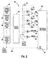
- a Phy interface 22 resides between the memory controller 18 and the physical memory devices.
- the Phy interface is typically located in the central processing unit but may be located elsewhere. For purposes of clarity, the Phy interface 22 is shown as a separate block in Figure 1 .
- the Phy interface generally includes circuitry for handling the timing requirements of the main memory data strobes.
- double data rate encompasses DDR1 / DDR2 / DDR 3 and/or subsequent generations of such memory devices.
- DDR memory devices typically conform to Joint Electron Devices Engineering Councils (JEDEC) standards. These standards define how DDR memory data is accessed (read), and stored (written). It should be understood that a Phy interface may be constructed to operate with other memory types and/or other memory standards.
- DQ data 32 and DQS (data strobe) 34.
- Other signals include the memory clock (MEMCLK) 38 as well as address and command signals (shown generally as ADDR/CMD 36).
- MEMCLK memory clock
- ADDR/CMD 36 address and command signals
- a DDR SDRAM issues DQ and DQS at the same time, a manner commonly referred to as "edge aligned."
- the Phy interface 22 utilizes delay circuitry, such as a delay-locked loop (DLL), to delay the DQS signal so that it may be used to correctly latch the DQ signals during a valid data window or "data eye”.
- the Phy interface 22 also utilizes delay circuitry to support the writing of data to the DDR DRAM.
- the DQS 34 For reading data, the DQS 34 must be delayed.
- the DQS and DQ 34, 32 must be delayed.
- the Phy interface 22 includes a plurality of command and status registers (CSRs) 42 that are utilized to control delay timing, drive strengths and a variety of other parameters as described in more detail below. It should be understood that such circuitry may be duplicated on a per channel basis as well.
- CSRs command and status registers
- the Phy interface may also adjust or select transmitter drive strength and receiver termination impedance. Rather than use fixed timing delays, transmitter drive strength and receiver termination impedance, these parameters may be adjusted each time the computer system is turned on. This is typically accomplished with the assistance of a training program.
- the training program is typically stored in a basic input/output system (BIOS) memory device 26, but it may also be implemented within the device hardware.
- BIOS basic input/output system
- the training program executes an algorithm during power-on self-test (POST), which determines appropriate timing delays, drive strengths and termination impedances associated with many of the memory interface signals.
- POST power-on self-test
- Theses parameters are saved within the Phy interface in a plurality of registers that define the overall timing of the various signal paths to and from the Phy. In the alternative, these parameters may be stored elsewhere (e.g., in the north bridge 14 or south bridge 16).
- Typical memory devices are also provided with a clock enable (self refresh) input 40.
- the clock enable input 40 is used to place the memory device in self refresh mode. In this mode, the memory device uses an on-chip timer to generate internal refresh cycles as necessary. External clocks may also be stopped during this time.
- This input is typically used in connection with power down modes since it allows the memory controller to be disabled without loss of main memory data.
- the DQ 32 (data) and DQS 34 (strobe) lines are bidirectional. It should be understood that each DIMM will have multiple DQ lines (e.g., 64 data bits) and multiple DQS lines. Each of these lines has an associated driver 52, 56 and receiver 54, 58 in the Phy interface 22. A single driver/receiver pair is shown in Figure 2 for purposes of clarity. Each driver has a selectable or adjustable drive output. Similarly, each receiver has a selectable or adjustable termination impedance (e.g., on die termination).
- the DQ and DQS lines 32, 34 are also associated with delay elements such as delay locked loops (DLLs) 72, 74, 76.
- DLLs delay locked loops
- Adjustments to delay elements are accomplished via programming appropriate values into the proper field of an associated CSR 42 as described in more detail below.
- the logical connection between CSRs and adjustments in delay elements, drive strength or termination impedance are shown generally in dashed lines.
- the Phy interface may dynamically change the DLL settings on a burst-by-burst (or transaction) basis.
- the Phy interface may store an optimum tupple of delay settings for DQ and DQS for each DIMM in the system. Depending upon the DIMM being accessed, the Phy interface retrieves the appropriate DLL settings and applies them.
- the Phy interface may tailor its demanded power based upon the desired level of performance. It should be understood that the determination of when to change power contexts may come from a variety of sources. For example, the operating system may determine that a context change is desired (e.g., after a set period of inactivity, by user command, time schedule or the like). In the alternative, hardware may be used to determine when a context change is desired.
- the context change is accomplished by switching between different sets of Phy interface parameters associated with different power states. For example, a high power state (e.g., higher memory speed) and a low power state (e.g., lower memory speed). Each power state has an associated set of Phy interface parameters or context (i.e., delay element settings, drive strengths and termination impedances for each signal line). As described in more detail hereafter, switching between power states may be accomplished in several ways. It should be understood that switching between multiple power states as disclosed herein can be applied to any memory type and is not limited to use with DDR memory as used in the examples below.
- the memory controller 18 may access the CSRs 42 via a 32-bit, time interleaved, uni-directional configuration bus 80.
- Address and command e.g., read, write, do nothing
- CSRs could be accessed via other communication links.
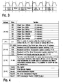
- the CSR address space is 16 bits wide, allowing for a space of 65,536 unique 16-bit registers. Instead of allowing for such a large space, the address is mapped to allow for the following functions: chiplet identification; intra-chiplet broadcast; compensation broadcast; chiplet instance identification (the D3DBYTE, D3CLK and D3CMP are chiplets that are placed more than once).
- Figure 4 shows a breakdown for CSRs addressing.
- a set of power context sensitive CSRs are provided for each power state.
- a first set of CSRs are associated with a first power context - PhyPS[0] 44.
- Another set of CSRs are associated with a second power context - PhyPS[1] 46.
- additional sets of CSRs may be provided to support more than two power contexts as shown by PhyPS[n] 48.
- a multiplexer or selection circuitry 50 is provided to select between the different sets of CSRs.
- the Phy interface also contains CSRs that are not power context sensitive. Such CSRs are applicable in all power states.
- Table 1 No. Description 1 DDR PLL rate; 2 DLL (Delay Locked Loop) frequency specific programming; 3 DQS (strobe bit) Drive Strength (DS); 4 DQ (date bit) DS 5 MemClk DS 6 Address & Command (Addr, Bank, RAS, CAS, WE, AddrParity) DS 7 Chip select (Cs) & On-die termination (Odt) DS 8 Clock Enable (Cke) DS 9 ProcOdt strength 10 ProcOdtOff 11 TxDqsDll control per Channel per DIMM per Byte 12 TxDqDll control per Channel per DIMM per Byte 13 RxEnDll control per Channel per DIMM per Byte 14 RxDqsLDll control per Channel per DIMM per nibble (used in x4 and x8 DIMM types) 15 RxDqsUDll control per Channel per DIMM per nibble (used in x4 and x8 DIMM types) 15 RxDqsUDll control per Channel per
- programming of the relevant fields of the Phy interface is accomplished by issuing commands or programming specific fields in CSRs via the configuration bus 80. For example, changing from one PhyPS to another may be accomplished with a single command issued to the DDR Phy interface indirect register space.
- Programming of PhyPS context sensitive CSRs may be accomplished by setting the appropriate PhyPS context and then performing normal indirect CSR writes or reads. Alternatively, direct CSR writes or reads may reach any CSR without regard to the PhyPS context.
- the Phy interface may be controlled via a series of commands including: Master_0x08[12] - PhyPS, Master_0x08[8] - PstateToAccess and Master_0x18[8] - PhyPSMasterChannel.
- the nomenclature [12], [8] and the like refers to the bit position within the command.
- the Master_0x08[12] command corresponds to the current Phy interface P-state (0 or 1). This command controls power context (e.g., which set of CSRs) is currently active.
- the Master_0x08[8] command selects which P-State to read or write to during CSR accesses. BIOS may use this method to control which P-State to write to without having to do an actual P-State change.
- the Master_0x18[8] command selects the master channel. In this embodiment, only the channel designated by this bit (master channel) is allowed to issue 0x0B[PhyPS Change] commands. Any 0x0B[PhyPS change] commands issued from other channels will be ignored. It should be understood that additional bits may be added to support more than two channels. In this embodiment, the following 0x0B commands are defined: Table 2 No. Description 1 Change PhyPS 2 Enter and exit PhySR (Self Refresh) 3 DDR rate change (i.e., change the DDR PLL frequency) 4 Update other Phy interface sub modes (via sub commands) 5 ⁇ PwrOk default settings
- the power context is selected via a single bit (i.e., PhyPS[0] and PhyPS[1] - bit position 26). It should be understood that additional bits may be added to support more than two contexts.
- the PhyPSRequest bit (bit position 30) is used to indicate that the command includes a context change.
- SR self refresh
- the entry into SR mode may happen at different times but all channels should be in SR mode before the context change.
- the Phy interface Upon receipt of the context change command, the Phy interface will change the PhyPS context, the DDR PLL multiplier and divider will be updated, and the PLL will be relocked. When this is all complete, CfgDone will be set. When SR mode is subsequently exited the DLLs will relock. During the time the PhyPS change is occurring the memory controller maintains control over all inputs to the Phy interface (specifically CKE, MemReset, ReadPending, WritePending, all other tri-state controls).
- the 0x0B command to enter and exit Phy interface Self Refresh may be issued in either channel 0 or 1; making it possible to have one DRAM channel in SR mode while the other is not.
- PhySR Phy interface Self Refresh
- 0x0B[25:24] control the behavior of the PLL while in SR. Entry into SR mode is very quick, taking ⁇ 300ns from receipt of the 0x0B command to the time CfgDone is asserted. To allow the memory controller to move forward as quickly as possible, the memory controller may monitor CfgDone for a transition from 1 to 0. This indicates the Phy interface has closed off input from the memory controller, driving all CKE low, driving MemReset appropriately and placing all remaining DDR bus pins into tristate. At this point it is safe for the memory controller to go proficient. It is not safe to drop the Vddr rail until CfgDone has asserted, indicating all necessary CSR transactions are complete.
- PhySR Phy interface clock grid
- PClk Phy interface clock grid
- the PLL may be left on or turned off during SR.
- the DDR rate is set first to load the CSRs containing the Phy interface PLL multiplier and divider.
- the 0x0B command for the DRAM data rate on the DDR bus is set by BIOS in channel 0 only. Sending 0x0B commands to set the DRAM data rate in channel 1 has no effect. It should be understood that other embodiments may support independent DDR data rates on each channel.
- BIOSes that understand Phy interface P-States should instead program the DDR Rates for both Phy interface PStates through the direct CSRs Master_0x00[DdrRate] and Master_0x40[DdrRate]. These rate changes (through the direct CSRs) will only take affect after a subsequent 0x0B[PhyPS change].
- the PhyPS state after cold reset, warm reset, or Advanced Configuration and Power Interface (ACPI) power state S3 (commonly referred to as Standby, Sleep, or Suspend to RAM) are shown in Table 6 below. All states are persistent through warm reset. Therefore, in the warm reset entries below, the values remain as they were prior to the warm reset.
- ACPI Advanced Configuration and Power Interface
- DDR3 requires a two pass training procedure to have an unambiguous convergence of Write Levelization (WL) and RxEn, it is possible to train for the lower-frequency PState as part of the process of training for the higher-powered PState.
- the procedure also assumes that BIOS has already determined that this is a cold reset (and thus requires training), as opposed to a warm reset or S3 exit.
- the PhyPS context is PhyPS0. Both channels, if memory is present, are ready to begin training. Training follows the known protocols such as the AMD Generic Encapsulated Software Architecture (AGESA) bootstrap protocol as shown generally in Table 8: Table 8 Description 6 Set all Drive Strengths fields. 7 Set NB_TxChnClkEn, perform hardware-based fence training, note and set the final Fence Value. 8 Set Address/Bank/RAS/CAS/WE/MemClk Dll launch delay. 9 Set Cs & Odt Dll launch delay. 10 Set Cke Dll launch delay. 11 Execute DRAM init. 12 Perform hardware-based WL training using default constants. 13 Perform hardware-based RxEn training using default constants. 14 Perform TxDq/RxDqs write/read training. 15 MRL training may occur here or it may occur later. NCLK must be running at the eventual target speed for this DDR rate.
- AGESA AMD Generic Encapsulated Software Architecture
- This DDR rate and other parameters established during this initial training protocol may be used as a first power context (e.g., lower speed - PhyPS[1]). It should be understood that PhyPS[1] may be set based on another DDR rate (i.e., repeat steps 4 through 15 for this frequency).
- the next phase trains for the higher (PhyPS[0]) DDR rate.
- the Write Levelization and RxEn training values are scaled by the MemClk data rate ratio PhyPS0/PhyPS1 and used as the seed for the second phase of training in PhyPS[0].
- the PhyPS context is still PhyPS[0], and the Phy interface is running at the PhyPS[0] DDR Rate. Both channels, if memory is present, are ready to begin the next phase of training as shown generally in Table 8: Table 10 Description 19 Set all Drive Strengths fields. 20 Set NB_TxChnClkEn, perform hardware-based fence training, note and set the final FenceValue. 21 Set Address/Bank/RAS/CAS/WE/MemClk Dll launch delay. 22 Set Cs & Odt Dll launch delay. 23 Set Cke Dll launch delay. 24 Execute DRAM init. 25 Perform hardware-based WL training using default constants. 26 Perform hardware-based RxEn training using default constants. 27 Perform TxDq/RxDqs write/read training. 28 MRL training may occur here or it may occur later. NCLK must be running at the eventual target speed for this DDR rate.
- BIOS may choose which PhyPS context should be used. In order to preserve historical meaning, BIOS may configure the Phy interface for PhyPS[0].
- Resumption from S3 does not involve any DRAM training, only restoring the trained values from nonvolatile state (generally in the South Bridge). Resumption from S3 will typically guarantee (because of ⁇ PwrOk) that the PhyPS context is PhyPS0, Master_0x08[PStateToAccess] is 0, that both channels are out of PhySR, and that the master channel is channel 0 (even if memory is not present on channel 0).
- the procedure for resuming from S3 are generally shown in Table 12: Table 12 Description 1 Put all active channels into SR. 2 If there is no memory on channel 0, set Master_0x18[PhyPSMasterChannel] (see 3.7) to ensure PhyPS changes being issued on channel 1 by the only active DCT have effect.
- a warm reset resume is almost identical to a resume from S3.
- Resume from S3 has ⁇ PwrOk set the PhyPS context to PhyPS0, designate channel 0 as the master channel to communicate PhyPS changes and take the Phy interface out of PhySR in both channels.
- warm reset leaves the PhyPS and PhySR as well as master channel in an unknown state.
- an architectural hole exists with a warm reset resume. If a warm reset resume is issued before the system may cold boot, complete memory training and store all trained values in non-volatile memory, the resume will fail.
- BIOS should use a flag (which is reset on cold reset but persistent through warm reset) to indicate whether the training values have been calculated and stored successfully - if during a warm reset, BIOS sees this flag set, it may resume by restoring the trained state.
- the trained state also includes the Master_0x18[PhyPSMasterChannel] as well as any unpopulated channel is left in SR mode. If this flag is not set then BIOS must (re)train the Phy. For purposes of the following disclosure, it is assumed that this flag has been set and that training values have been stored. Therefore warm reset resume does not involve any DRAM training, only restoring the trained values from non-volatile state (generally in the South Bridge).
- Table 14 shows a list of all PhyPS CSRs that are duplicated for each power context: Table 14 Description 1 Master_0x00[Config0] for PhyPS0 2 Master_0x40[Config0] for PhyPS1 3 Master_0x01[Config1] for PhyPS0 4 Master_0x41[Config1] for PhyPS1 5 Master_0x02[AddrCmdCke] for PhyPS0 6 Master_0x42[AddrCmdCke] for PhyPS1 7 Master_0x03 [PllDiv, PllMult, PllDiv2Bypass, PllUpdate] will now be for PhyPS0 PLL control 8 Master_0x43[PllDiv, PllMult, PllDiv2Bypass, PllUpdate] will now be for PhvPS1 PLL control 9 8:0.DByte_0x ⁇ 00,04,08 ⁇ are the PhyPS0 DS and POdt control 10 8:0.DByte_0x
- multiple power contexts could be stored in other memory locations (e.g., in the north bridge 14 or south bridge 16).
- a standard Phy interface could switch power contexts without the need for a dedicated set of context sensitive CSRs.
- Such a scenario could eliminate the need for multiple sets of CSRs but would increase the latency for the context change.
- ROM read only memory
- RAM random access memory
- register cache memory
- semiconductor memory devices magnetic media such as internal hard disks and removable disks, magneto-optical media, and optical media such as CD-ROM disks, and digital versatile disks (DVDs).
- Suitable processors include, by way of example, a general purpose processor, a special purpose processor, a conventional processor, a digital signal processor (DSP), a plurality of microprocessors, one or more microprocessors in association with a DSP core, a controller, a microcontroller, Application Specific Integrated Circuits (ASICs), Field Programmable Gate Arrays (FPGAs) circuits, any other type of integrated circuit (IC), and/or a state machine.
- DSP digital signal processor
- ASICs Application Specific Integrated Circuits
- FPGAs Field Programmable Gate Arrays
- Such processors may be manufactured by configuring a manufacturing process using the results of processed hardware description language (HDL) instructions (such instructions capable of being stored on a computer readable media). The results of such processing may be maskworks that are then used in a semiconductor manufacturing process to manufacture a processor which implements aspects of the present invention.
- HDL hardware description language
Landscapes
- Engineering & Computer Science (AREA)
- Theoretical Computer Science (AREA)
- General Engineering & Computer Science (AREA)
- Physics & Mathematics (AREA)
- General Physics & Mathematics (AREA)
- Computer Hardware Design (AREA)
- Dram (AREA)
- Power Sources (AREA)
Applications Claiming Priority (3)
| Application Number | Priority Date | Filing Date | Title |
|---|---|---|---|
| US38208910P | 2010-09-13 | 2010-09-13 | |
| US12/910,412 US8356155B2 (en) | 2010-09-13 | 2010-10-22 | Dynamic RAM Phy interface with configurable power states |
| PCT/US2011/051345 WO2012037086A1 (en) | 2010-09-13 | 2011-09-13 | Dynamic ram phy interface with configurable power states |
Publications (2)
| Publication Number | Publication Date |
|---|---|
| EP2616946A1 EP2616946A1 (en) | 2013-07-24 |
| EP2616946B1 true EP2616946B1 (en) | 2014-06-04 |
Family
ID=44674909
Family Applications (1)
| Application Number | Title | Priority Date | Filing Date |
|---|---|---|---|
| EP11760647.5A Active EP2616946B1 (en) | 2010-09-13 | 2011-09-13 | Dynamic ram phy interface with configurable power states |
Country Status (6)
| Country | Link |
|---|---|
| US (2) | US8356155B2 (enExample) |
| EP (1) | EP2616946B1 (enExample) |
| JP (1) | JP5955323B2 (enExample) |
| KR (1) | KR101879707B1 (enExample) |
| CN (1) | CN103168296B (enExample) |
| WO (1) | WO2012037086A1 (enExample) |
Cited By (2)
| Publication number | Priority date | Publication date | Assignee | Title |
|---|---|---|---|---|
| WO2015200338A1 (en) * | 2014-06-27 | 2015-12-30 | Advanced Micro Devices, Inc. | Integrated controller for training memory physical layer interface |
| US10275386B2 (en) | 2014-06-27 | 2019-04-30 | Advanced Micro Devices, Inc. | Memory physical layer interface logic for generating dynamic random access memory (DRAM) commands with programmable delays |
Families Citing this family (26)
| Publication number | Priority date | Publication date | Assignee | Title |
|---|---|---|---|---|
| US8799553B2 (en) * | 2010-04-13 | 2014-08-05 | Apple Inc. | Memory controller mapping on-the-fly |
| US9363115B2 (en) * | 2012-07-02 | 2016-06-07 | Taiwan Semiconductor Manufacturing Co., Ltd. | System and method for aligning data bits |
| JP6184064B2 (ja) * | 2012-07-19 | 2017-08-23 | インターナショナル・ビジネス・マシーンズ・コーポレーションInternational Business Machines Corporation | メモリサブシステム、コンピュータ・システム |
| TWI493566B (zh) * | 2012-10-15 | 2015-07-21 | Via Tech Inc | 資料儲存裝置、儲存媒體控制器與控制方法 |
| US9305632B2 (en) | 2013-04-29 | 2016-04-05 | Qualcomm Incorporated | Frequency power manager |
| US9123408B2 (en) | 2013-05-24 | 2015-09-01 | Qualcomm Incorporated | Low latency synchronization scheme for mesochronous DDR system |
| KR101925694B1 (ko) | 2013-12-26 | 2018-12-05 | 인텔 코포레이션 | 멀티칩 패키지 링크 |
| KR20160029392A (ko) | 2014-09-05 | 2016-03-15 | 에스케이하이닉스 주식회사 | 임피던스 조정 회로 및 이를 이용한 반도체 메모리와 메모리 시스템 |
| US9733957B2 (en) * | 2014-09-05 | 2017-08-15 | Qualcomm Incorporated | Frequency and power management |
| CN104536917B (zh) * | 2015-01-19 | 2017-04-26 | 中国电子科技集团公司第二十四研究所 | 应用于fpaa的基于存储器的多功能动态配置电路 |
| US10409357B1 (en) * | 2016-09-30 | 2019-09-10 | Cadence Design Systems, Inc. | Command-oriented low power control method of high-bandwidth-memory system |
| JP2018101835A (ja) * | 2016-12-19 | 2018-06-28 | 株式会社東芝 | 携帯可能電子装置、及びicカード |
| KR102340446B1 (ko) * | 2017-09-08 | 2021-12-21 | 삼성전자주식회사 | 스토리지 장치 및 그것의 데이터 트레이닝 방법 |
| CN110347620A (zh) * | 2019-05-29 | 2019-10-18 | 深圳市紫光同创电子有限公司 | 一种fpga电路和系统 |
| US20210200298A1 (en) * | 2019-12-30 | 2021-07-01 | Advanced Micro Devices, Inc. | Long-idle state system and method |
| US11176986B2 (en) * | 2019-12-30 | 2021-11-16 | Advanced Micro Devices, Inc. | Memory context restore, reduction of boot time of a system on a chip by reducing double data rate memory training |
| US11100028B1 (en) | 2020-04-27 | 2021-08-24 | Apex Semiconductor | Programmable I/O switch/bridge chiplet |
| US12322433B2 (en) | 2020-12-22 | 2025-06-03 | Intel Corporation | Power and performance optimization in a memory subsystem |
| US11609879B2 (en) * | 2021-02-26 | 2023-03-21 | Nvidia Corporation | Techniques for configuring parallel processors for different application domains |
| US12437827B2 (en) * | 2021-12-29 | 2025-10-07 | Advanced Micro Devices, Inc. | DRAM specific interface calibration via programmable training sequences |
| US12079490B2 (en) * | 2021-12-29 | 2024-09-03 | Advanced Micro Devices, Inc. | Reducing power consumption associated with frequency transitioning in a memory interface |
| CN114492286B (zh) * | 2022-01-18 | 2025-02-14 | Oppo广东移动通信有限公司 | 控制芯片的方法及装置 |
| CN115344215B (zh) * | 2022-08-29 | 2025-03-18 | 深圳市紫光同创电子股份有限公司 | 存储器训练方法及系统 |
| US12072381B2 (en) | 2022-10-18 | 2024-08-27 | Micron Technology, Inc. | Multi-modal memory apparatuses and systems |
| US20240355379A1 (en) * | 2023-04-21 | 2024-10-24 | Advanced Micro Devices, Inc. | Voltage Range for Training Physical Memory |
| WO2025024727A1 (en) * | 2023-07-26 | 2025-01-30 | Advanced Micro Devices, Inc. | Memory self-refresh power gating |
Family Cites Families (21)
| Publication number | Priority date | Publication date | Assignee | Title |
|---|---|---|---|---|
| US4631659A (en) * | 1984-03-08 | 1986-12-23 | Texas Instruments Incorporated | Memory interface with automatic delay state |
| US6154821A (en) * | 1998-03-10 | 2000-11-28 | Rambus Inc. | Method and apparatus for initializing dynamic random access memory (DRAM) devices by levelizing a read domain |
| US6401213B1 (en) * | 1999-07-09 | 2002-06-04 | Micron Technology, Inc. | Timing circuit for high speed memory |
| JP5034133B2 (ja) * | 2000-02-29 | 2012-09-26 | 富士通セミコンダクター株式会社 | 半導体記憶装置 |
| AU2001296911A1 (en) * | 2000-09-26 | 2002-04-08 | Sun Microsystems, Inc. | Method and apparatus for reducing power consumption |
| US6618791B1 (en) * | 2000-09-29 | 2003-09-09 | Intel Corporation | System and method for controlling power states of a memory device via detection of a chip select signal |
| US6788593B2 (en) * | 2001-02-28 | 2004-09-07 | Rambus, Inc. | Asynchronous, high-bandwidth memory component using calibrated timing elements |
| KR100403347B1 (ko) * | 2001-09-14 | 2003-11-01 | 주식회사 하이닉스반도체 | 반도체 메모리 장치의 파워-업 발생회로 |
| US7000065B2 (en) * | 2002-01-02 | 2006-02-14 | Intel Corporation | Method and apparatus for reducing power consumption in a memory bus interface by selectively disabling and enabling sense amplifiers |
| US6816994B2 (en) * | 2002-06-21 | 2004-11-09 | Micron Technology, Inc. | Low power buffer implementation |
| US7234099B2 (en) * | 2003-04-14 | 2007-06-19 | International Business Machines Corporation | High reliability memory module with a fault tolerant address and command bus |
| US6876593B2 (en) * | 2003-07-01 | 2005-04-05 | Intel Corporation | Method and apparatus for partial refreshing of DRAMS |
| US20050198542A1 (en) | 2004-03-08 | 2005-09-08 | David Freker | Method and apparatus for a variable memory enable deassertion wait time |
| US7386654B2 (en) | 2004-10-15 | 2008-06-10 | Intel Corporation | Non-volatile configuration data storage for a configurable memory |
| KR100673904B1 (ko) * | 2005-04-30 | 2007-01-25 | 주식회사 하이닉스반도체 | 반도체메모리소자 |
| US7471130B2 (en) * | 2005-05-19 | 2008-12-30 | Micron Technology, Inc. | Graduated delay line for increased clock skew correction circuit operating range |
| US8244971B2 (en) * | 2006-07-31 | 2012-08-14 | Google Inc. | Memory circuit system and method |
| JP4615461B2 (ja) * | 2006-03-10 | 2011-01-19 | 京セラミタ株式会社 | メモリコントローラ |
| JP2007249738A (ja) * | 2006-03-17 | 2007-09-27 | Kawasaki Microelectronics Kk | メモリアクセス制御装置 |
| US7869287B2 (en) | 2008-03-31 | 2011-01-11 | Advanced Micro Devices, Inc. | Circuit for locking a delay locked loop (DLL) and method therefor |
| JP2010160724A (ja) * | 2009-01-09 | 2010-07-22 | Ricoh Co Ltd | メモリ制御システム、メモリ制御方法、メモリ制御プログラム及び記録媒体 |
-
2010
- 2010-10-22 US US12/910,412 patent/US8356155B2/en active Active
-
2011
- 2011-09-13 KR KR1020137009085A patent/KR101879707B1/ko active Active
- 2011-09-13 CN CN201180049362.4A patent/CN103168296B/zh active Active
- 2011-09-13 EP EP11760647.5A patent/EP2616946B1/en active Active
- 2011-09-13 WO PCT/US2011/051345 patent/WO2012037086A1/en not_active Ceased
- 2011-09-13 JP JP2013529258A patent/JP5955323B2/ja active Active
-
2013
- 2013-01-09 US US13/737,306 patent/US9274938B2/en active Active
Cited By (2)
| Publication number | Priority date | Publication date | Assignee | Title |
|---|---|---|---|---|
| WO2015200338A1 (en) * | 2014-06-27 | 2015-12-30 | Advanced Micro Devices, Inc. | Integrated controller for training memory physical layer interface |
| US10275386B2 (en) | 2014-06-27 | 2019-04-30 | Advanced Micro Devices, Inc. | Memory physical layer interface logic for generating dynamic random access memory (DRAM) commands with programmable delays |
Also Published As
| Publication number | Publication date |
|---|---|
| CN103168296A (zh) | 2013-06-19 |
| WO2012037086A1 (en) | 2012-03-22 |
| JP2013543612A (ja) | 2013-12-05 |
| US9274938B2 (en) | 2016-03-01 |
| KR101879707B1 (ko) | 2018-07-18 |
| US8356155B2 (en) | 2013-01-15 |
| JP5955323B2 (ja) | 2016-07-20 |
| US20120066445A1 (en) | 2012-03-15 |
| US20130124806A1 (en) | 2013-05-16 |
| KR20140007331A (ko) | 2014-01-17 |
| EP2616946A1 (en) | 2013-07-24 |
| CN103168296B (zh) | 2016-08-03 |
Similar Documents
| Publication | Publication Date | Title |
|---|---|---|
| EP2616946B1 (en) | Dynamic ram phy interface with configurable power states | |
| US10872652B2 (en) | Method and apparatus for optimizing calibrations of a memory subsystem | |
| US6263448B1 (en) | Power control system for synchronous memory device | |
| US8619492B2 (en) | On-die termination circuit, memory device, memory module, and method of operating and training an on-die termination | |
| KR102444201B1 (ko) | 플랫폼 마지닝 및 디버그를 위한 소프트웨어 모드 레지스터 액세스 | |
| TWI895084B (zh) | 記憶體中的增強型資料時鐘操作 | |
| US20100246294A1 (en) | System and method for delay locked loop relock mode | |
| US20120117402A1 (en) | Memory Read Timing Margin Adjustment | |
| GB2470631A (en) | Registered memory module | |
| US10719058B1 (en) | System and method for memory control having selectively distributed power-on processing | |
| US20150194196A1 (en) | Memory system with high performance and high power efficiency and control method of the same | |
| CN112041925A (zh) | 用于在读取操作期间控制数据选通信号的系统及方法 | |
| US7039817B2 (en) | Method and apparatus for supplying power to a processor at a controlled voltage | |
| US20080052481A1 (en) | Method and circuit for transmitting a memory clock signal | |
| EP4202604B1 (en) | Fast self-refresh exit power state | |
| US8379459B2 (en) | Memory system with delay locked loop (DLL) bypass control | |
| US11934251B2 (en) | Data fabric clock switching |
Legal Events
| Date | Code | Title | Description |
|---|---|---|---|
| PUAI | Public reference made under article 153(3) epc to a published international application that has entered the european phase |
Free format text: ORIGINAL CODE: 0009012 |
|
| 17P | Request for examination filed |
Effective date: 20130402 |
|
| AK | Designated contracting states |
Kind code of ref document: A1 Designated state(s): AL AT BE BG CH CY CZ DE DK EE ES FI FR GB GR HR HU IE IS IT LI LT LU LV MC MK MT NL NO PL PT RO RS SE SI SK SM TR |
|
| DAX | Request for extension of the european patent (deleted) | ||
| GRAP | Despatch of communication of intention to grant a patent |
Free format text: ORIGINAL CODE: EPIDOSNIGR1 |
|
| INTG | Intention to grant announced |
Effective date: 20140110 |
|
| GRAS | Grant fee paid |
Free format text: ORIGINAL CODE: EPIDOSNIGR3 |
|
| GRAA | (expected) grant |
Free format text: ORIGINAL CODE: 0009210 |
|
| AK | Designated contracting states |
Kind code of ref document: B1 Designated state(s): AL AT BE BG CH CY CZ DE DK EE ES FI FR GB GR HR HU IE IS IT LI LT LU LV MC MK MT NL NO PL PT RO RS SE SI SK SM TR |
|
| REG | Reference to a national code |
Ref country code: GB Ref legal event code: FG4D |
|
| REG | Reference to a national code |
Ref country code: CH Ref legal event code: EP |
|
| REG | Reference to a national code |
Ref country code: AT Ref legal event code: REF Ref document number: 671426 Country of ref document: AT Kind code of ref document: T Effective date: 20140615 |
|
| REG | Reference to a national code |
Ref country code: IE Ref legal event code: FG4D |
|
| REG | Reference to a national code |
Ref country code: DE Ref legal event code: R096 Ref document number: 602011007494 Country of ref document: DE Effective date: 20140717 |
|
| REG | Reference to a national code |
Ref country code: AT Ref legal event code: MK05 Ref document number: 671426 Country of ref document: AT Kind code of ref document: T Effective date: 20140604 |
|
| REG | Reference to a national code |
Ref country code: NL Ref legal event code: VDEP Effective date: 20140604 |
|
| PG25 | Lapsed in a contracting state [announced via postgrant information from national office to epo] |
Ref country code: CY Free format text: LAPSE BECAUSE OF FAILURE TO SUBMIT A TRANSLATION OF THE DESCRIPTION OR TO PAY THE FEE WITHIN THE PRESCRIBED TIME-LIMIT Effective date: 20140604 Ref country code: FI Free format text: LAPSE BECAUSE OF FAILURE TO SUBMIT A TRANSLATION OF THE DESCRIPTION OR TO PAY THE FEE WITHIN THE PRESCRIBED TIME-LIMIT Effective date: 20140604 Ref country code: NO Free format text: LAPSE BECAUSE OF FAILURE TO SUBMIT A TRANSLATION OF THE DESCRIPTION OR TO PAY THE FEE WITHIN THE PRESCRIBED TIME-LIMIT Effective date: 20140904 Ref country code: GR Free format text: LAPSE BECAUSE OF FAILURE TO SUBMIT A TRANSLATION OF THE DESCRIPTION OR TO PAY THE FEE WITHIN THE PRESCRIBED TIME-LIMIT Effective date: 20140905 Ref country code: LT Free format text: LAPSE BECAUSE OF FAILURE TO SUBMIT A TRANSLATION OF THE DESCRIPTION OR TO PAY THE FEE WITHIN THE PRESCRIBED TIME-LIMIT Effective date: 20140604 |
|
| REG | Reference to a national code |
Ref country code: LT Ref legal event code: MG4D |
|
| PG25 | Lapsed in a contracting state [announced via postgrant information from national office to epo] |
Ref country code: LV Free format text: LAPSE BECAUSE OF FAILURE TO SUBMIT A TRANSLATION OF THE DESCRIPTION OR TO PAY THE FEE WITHIN THE PRESCRIBED TIME-LIMIT Effective date: 20140604 Ref country code: RS Free format text: LAPSE BECAUSE OF FAILURE TO SUBMIT A TRANSLATION OF THE DESCRIPTION OR TO PAY THE FEE WITHIN THE PRESCRIBED TIME-LIMIT Effective date: 20140604 Ref country code: SE Free format text: LAPSE BECAUSE OF FAILURE TO SUBMIT A TRANSLATION OF THE DESCRIPTION OR TO PAY THE FEE WITHIN THE PRESCRIBED TIME-LIMIT Effective date: 20140604 Ref country code: AT Free format text: LAPSE BECAUSE OF FAILURE TO SUBMIT A TRANSLATION OF THE DESCRIPTION OR TO PAY THE FEE WITHIN THE PRESCRIBED TIME-LIMIT Effective date: 20140604 Ref country code: HR Free format text: LAPSE BECAUSE OF FAILURE TO SUBMIT A TRANSLATION OF THE DESCRIPTION OR TO PAY THE FEE WITHIN THE PRESCRIBED TIME-LIMIT Effective date: 20140604 |
|
| PG25 | Lapsed in a contracting state [announced via postgrant information from national office to epo] |
Ref country code: CZ Free format text: LAPSE BECAUSE OF FAILURE TO SUBMIT A TRANSLATION OF THE DESCRIPTION OR TO PAY THE FEE WITHIN THE PRESCRIBED TIME-LIMIT Effective date: 20140604 Ref country code: SK Free format text: LAPSE BECAUSE OF FAILURE TO SUBMIT A TRANSLATION OF THE DESCRIPTION OR TO PAY THE FEE WITHIN THE PRESCRIBED TIME-LIMIT Effective date: 20140604 Ref country code: RO Free format text: LAPSE BECAUSE OF FAILURE TO SUBMIT A TRANSLATION OF THE DESCRIPTION OR TO PAY THE FEE WITHIN THE PRESCRIBED TIME-LIMIT Effective date: 20140604 Ref country code: PT Free format text: LAPSE BECAUSE OF FAILURE TO SUBMIT A TRANSLATION OF THE DESCRIPTION OR TO PAY THE FEE WITHIN THE PRESCRIBED TIME-LIMIT Effective date: 20141006 Ref country code: EE Free format text: LAPSE BECAUSE OF FAILURE TO SUBMIT A TRANSLATION OF THE DESCRIPTION OR TO PAY THE FEE WITHIN THE PRESCRIBED TIME-LIMIT Effective date: 20140604 Ref country code: ES Free format text: LAPSE BECAUSE OF FAILURE TO SUBMIT A TRANSLATION OF THE DESCRIPTION OR TO PAY THE FEE WITHIN THE PRESCRIBED TIME-LIMIT Effective date: 20140604 |
|
| PG25 | Lapsed in a contracting state [announced via postgrant information from national office to epo] |
Ref country code: PL Free format text: LAPSE BECAUSE OF FAILURE TO SUBMIT A TRANSLATION OF THE DESCRIPTION OR TO PAY THE FEE WITHIN THE PRESCRIBED TIME-LIMIT Effective date: 20140604 Ref country code: IS Free format text: LAPSE BECAUSE OF FAILURE TO SUBMIT A TRANSLATION OF THE DESCRIPTION OR TO PAY THE FEE WITHIN THE PRESCRIBED TIME-LIMIT Effective date: 20141004 Ref country code: NL Free format text: LAPSE BECAUSE OF FAILURE TO SUBMIT A TRANSLATION OF THE DESCRIPTION OR TO PAY THE FEE WITHIN THE PRESCRIBED TIME-LIMIT Effective date: 20140604 |
|
| REG | Reference to a national code |
Ref country code: DE Ref legal event code: R097 Ref document number: 602011007494 Country of ref document: DE |
|
| PLBE | No opposition filed within time limit |
Free format text: ORIGINAL CODE: 0009261 |
|
| STAA | Information on the status of an ep patent application or granted ep patent |
Free format text: STATUS: NO OPPOSITION FILED WITHIN TIME LIMIT |
|
| PG25 | Lapsed in a contracting state [announced via postgrant information from national office to epo] |
Ref country code: LU Free format text: LAPSE BECAUSE OF FAILURE TO SUBMIT A TRANSLATION OF THE DESCRIPTION OR TO PAY THE FEE WITHIN THE PRESCRIBED TIME-LIMIT Effective date: 20140913 Ref country code: MC Free format text: LAPSE BECAUSE OF FAILURE TO SUBMIT A TRANSLATION OF THE DESCRIPTION OR TO PAY THE FEE WITHIN THE PRESCRIBED TIME-LIMIT Effective date: 20140604 Ref country code: IT Free format text: LAPSE BECAUSE OF FAILURE TO SUBMIT A TRANSLATION OF THE DESCRIPTION OR TO PAY THE FEE WITHIN THE PRESCRIBED TIME-LIMIT Effective date: 20140604 Ref country code: DK Free format text: LAPSE BECAUSE OF FAILURE TO SUBMIT A TRANSLATION OF THE DESCRIPTION OR TO PAY THE FEE WITHIN THE PRESCRIBED TIME-LIMIT Effective date: 20140604 |
|
| REG | Reference to a national code |
Ref country code: CH Ref legal event code: PL |
|
| 26N | No opposition filed |
Effective date: 20150305 |
|
| REG | Reference to a national code |
Ref country code: IE Ref legal event code: MM4A |
|
| REG | Reference to a national code |
Ref country code: DE Ref legal event code: R097 Ref document number: 602011007494 Country of ref document: DE Effective date: 20150305 |
|
| REG | Reference to a national code |
Ref country code: FR Ref legal event code: ST Effective date: 20150529 |
|
| PG25 | Lapsed in a contracting state [announced via postgrant information from national office to epo] |
Ref country code: SI Free format text: LAPSE BECAUSE OF FAILURE TO SUBMIT A TRANSLATION OF THE DESCRIPTION OR TO PAY THE FEE WITHIN THE PRESCRIBED TIME-LIMIT Effective date: 20140604 Ref country code: CH Free format text: LAPSE BECAUSE OF NON-PAYMENT OF DUE FEES Effective date: 20140930 Ref country code: LI Free format text: LAPSE BECAUSE OF NON-PAYMENT OF DUE FEES Effective date: 20140930 |
|
| PG25 | Lapsed in a contracting state [announced via postgrant information from national office to epo] |
Ref country code: FR Free format text: LAPSE BECAUSE OF NON-PAYMENT OF DUE FEES Effective date: 20140930 Ref country code: IE Free format text: LAPSE BECAUSE OF NON-PAYMENT OF DUE FEES Effective date: 20140913 |
|
| PG25 | Lapsed in a contracting state [announced via postgrant information from national office to epo] |
Ref country code: SM Free format text: LAPSE BECAUSE OF FAILURE TO SUBMIT A TRANSLATION OF THE DESCRIPTION OR TO PAY THE FEE WITHIN THE PRESCRIBED TIME-LIMIT Effective date: 20140604 |
|
| PG25 | Lapsed in a contracting state [announced via postgrant information from national office to epo] |
Ref country code: MT Free format text: LAPSE BECAUSE OF FAILURE TO SUBMIT A TRANSLATION OF THE DESCRIPTION OR TO PAY THE FEE WITHIN THE PRESCRIBED TIME-LIMIT Effective date: 20140604 Ref country code: BG Free format text: LAPSE BECAUSE OF FAILURE TO SUBMIT A TRANSLATION OF THE DESCRIPTION OR TO PAY THE FEE WITHIN THE PRESCRIBED TIME-LIMIT Effective date: 20140604 |
|
| PG25 | Lapsed in a contracting state [announced via postgrant information from national office to epo] |
Ref country code: BE Free format text: LAPSE BECAUSE OF FAILURE TO SUBMIT A TRANSLATION OF THE DESCRIPTION OR TO PAY THE FEE WITHIN THE PRESCRIBED TIME-LIMIT Effective date: 20140604 Ref country code: HU Free format text: LAPSE BECAUSE OF FAILURE TO SUBMIT A TRANSLATION OF THE DESCRIPTION OR TO PAY THE FEE WITHIN THE PRESCRIBED TIME-LIMIT; INVALID AB INITIO Effective date: 20110913 |
|
| PG25 | Lapsed in a contracting state [announced via postgrant information from national office to epo] |
Ref country code: TR Free format text: LAPSE BECAUSE OF FAILURE TO SUBMIT A TRANSLATION OF THE DESCRIPTION OR TO PAY THE FEE WITHIN THE PRESCRIBED TIME-LIMIT Effective date: 20140604 |
|
| PG25 | Lapsed in a contracting state [announced via postgrant information from national office to epo] |
Ref country code: MK Free format text: LAPSE BECAUSE OF FAILURE TO SUBMIT A TRANSLATION OF THE DESCRIPTION OR TO PAY THE FEE WITHIN THE PRESCRIBED TIME-LIMIT Effective date: 20140604 |
|
| PG25 | Lapsed in a contracting state [announced via postgrant information from national office to epo] |
Ref country code: AL Free format text: LAPSE BECAUSE OF FAILURE TO SUBMIT A TRANSLATION OF THE DESCRIPTION OR TO PAY THE FEE WITHIN THE PRESCRIBED TIME-LIMIT Effective date: 20140604 |
|
| P01 | Opt-out of the competence of the unified patent court (upc) registered |
Effective date: 20230530 |
|
| PGFP | Annual fee paid to national office [announced via postgrant information from national office to epo] |
Ref country code: DE Payment date: 20250819 Year of fee payment: 15 |
|
| PGFP | Annual fee paid to national office [announced via postgrant information from national office to epo] |
Ref country code: GB Payment date: 20250911 Year of fee payment: 15 |