EP2616831B1 - Kalibriereinheit für ein messgerät - Google Patents
Kalibriereinheit für ein messgerät Download PDFInfo
- Publication number
- EP2616831B1 EP2616831B1 EP11758142.1A EP11758142A EP2616831B1 EP 2616831 B1 EP2616831 B1 EP 2616831B1 EP 11758142 A EP11758142 A EP 11758142A EP 2616831 B1 EP2616831 B1 EP 2616831B1
- Authority
- EP
- European Patent Office
- Prior art keywords
- inner conductor
- connecting element
- housing
- segment
- part segment
- Prior art date
- Legal status (The legal status is an assumption and is not a legal conclusion. Google has not performed a legal analysis and makes no representation as to the accuracy of the status listed.)
- Active
Links
Images




Classifications
-
- G—PHYSICS
- G01—MEASURING; TESTING
- G01R—MEASURING ELECTRIC VARIABLES; MEASURING MAGNETIC VARIABLES
- G01R35/00—Testing or calibrating of apparatus covered by the other groups of this subclass
- G01R35/005—Calibrating; Standards or reference devices, e.g. voltage or resistance standards, "golden" references
-
- G—PHYSICS
- G01—MEASURING; TESTING
- G01R—MEASURING ELECTRIC VARIABLES; MEASURING MAGNETIC VARIABLES
- G01R35/00—Testing or calibrating of apparatus covered by the other groups of this subclass
- G01R35/005—Calibrating; Standards or reference devices, e.g. voltage or resistance standards, "golden" references
- G01R35/007—Standards or reference devices, e.g. voltage or resistance standards, "golden references"
-
- H—ELECTRICITY
- H01—ELECTRIC ELEMENTS
- H01P—WAVEGUIDES; RESONATORS, LINES, OR OTHER DEVICES OF THE WAVEGUIDE TYPE
- H01P1/00—Auxiliary devices
- H01P1/24—Terminating devices
-
- H—ELECTRICITY
- H01—ELECTRIC ELEMENTS
- H01R—ELECTRICALLY-CONDUCTIVE CONNECTIONS; STRUCTURAL ASSOCIATIONS OF A PLURALITY OF MUTUALLY-INSULATED ELECTRICAL CONNECTING ELEMENTS; COUPLING DEVICES; CURRENT COLLECTORS
- H01R13/00—Details of coupling devices of the kinds covered by groups H01R12/70 or H01R24/00 - H01R33/00
- H01R13/646—Details of coupling devices of the kinds covered by groups H01R12/70 or H01R24/00 - H01R33/00 specially adapted for high-frequency, e.g. structures providing an impedance match or phase match
-
- H—ELECTRICITY
- H01—ELECTRIC ELEMENTS
- H01R—ELECTRICALLY-CONDUCTIVE CONNECTIONS; STRUCTURAL ASSOCIATIONS OF A PLURALITY OF MUTUALLY-INSULATED ELECTRICAL CONNECTING ELEMENTS; COUPLING DEVICES; CURRENT COLLECTORS
- H01R24/00—Two-part coupling devices, or either of their cooperating parts, characterised by their overall structure
- H01R24/38—Two-part coupling devices, or either of their cooperating parts, characterised by their overall structure having concentrically or coaxially arranged contacts
- H01R24/40—Two-part coupling devices, or either of their cooperating parts, characterised by their overall structure having concentrically or coaxially arranged contacts specially adapted for high frequency
-
- H—ELECTRICITY
- H01—ELECTRIC ELEMENTS
- H01R—ELECTRICALLY-CONDUCTIVE CONNECTIONS; STRUCTURAL ASSOCIATIONS OF A PLURALITY OF MUTUALLY-INSULATED ELECTRICAL CONNECTING ELEMENTS; COUPLING DEVICES; CURRENT COLLECTORS
- H01R24/00—Two-part coupling devices, or either of their cooperating parts, characterised by their overall structure
- H01R24/38—Two-part coupling devices, or either of their cooperating parts, characterised by their overall structure having concentrically or coaxially arranged contacts
- H01R24/40—Two-part coupling devices, or either of their cooperating parts, characterised by their overall structure having concentrically or coaxially arranged contacts specially adapted for high frequency
- H01R24/42—Two-part coupling devices, or either of their cooperating parts, characterised by their overall structure having concentrically or coaxially arranged contacts specially adapted for high frequency comprising impedance matching means or electrical components, e.g. filters or switches
-
- G—PHYSICS
- G01—MEASURING; TESTING
- G01R—MEASURING ELECTRIC VARIABLES; MEASURING MAGNETIC VARIABLES
- G01R3/00—Apparatus or processes specially adapted for the manufacture or maintenance of measuring instruments, e.g. of probe tips
-
- H—ELECTRICITY
- H01—ELECTRIC ELEMENTS
- H01R—ELECTRICALLY-CONDUCTIVE CONNECTIONS; STRUCTURAL ASSOCIATIONS OF A PLURALITY OF MUTUALLY-INSULATED ELECTRICAL CONNECTING ELEMENTS; COUPLING DEVICES; CURRENT COLLECTORS
- H01R2103/00—Two poles
-
- Y—GENERAL TAGGING OF NEW TECHNOLOGICAL DEVELOPMENTS; GENERAL TAGGING OF CROSS-SECTIONAL TECHNOLOGIES SPANNING OVER SEVERAL SECTIONS OF THE IPC; TECHNICAL SUBJECTS COVERED BY FORMER USPC CROSS-REFERENCE ART COLLECTIONS [XRACs] AND DIGESTS
- Y10—TECHNICAL SUBJECTS COVERED BY FORMER USPC
- Y10T—TECHNICAL SUBJECTS COVERED BY FORMER US CLASSIFICATION
- Y10T156/00—Adhesive bonding and miscellaneous chemical manufacture
- Y10T156/10—Methods of surface bonding and/or assembly therefor
- Y10T156/1052—Methods of surface bonding and/or assembly therefor with cutting, punching, tearing or severing
- Y10T156/108—Flash, trim or excess removal
Definitions
- the invention relates to a calibration unit for an electronic measuring device, in particular for a network analyzer.
- Network analyzers used to determine scattering parameters of connected measurement objects e.g. of filters, amplifiers and attenuators cover a wide frequency range and reach ever higher upper limit frequencies. Via special step-up stages, the scattering parameters of measuring objects can be determined e.g. in the W band (75 GHz to 110 GHz).
- the individual components of a network analyzer are themselves faulty and have a frequency and phase response, which in particular at high frequencies leads to the fact that no more accurate statements from the measurement object are possible.
- a calibration of the network analyzer allows to compensate for these system errors, whereby the measurement accuracy is greatly increased.
- Such a calibration is carried out by successively connecting different calibration standards with known electrical properties to the measurement ports and determining the measured values.
- Known calibration standards are open, short, close, and through. In this case, for example, the standard calibration standard must achieve the highest possible signal attenuation over as wide a frequency range as possible, so that a good distinctness, for example, between the calibration standard conclusion of the calibration standard short circuit is ensured.
- the calibration standards idle, short-circuit and termination are present as coaxial connectors, which are screwed one after the other onto the individual coaxial measuring ports of the network analyzer.
- coaxial cables are used whose outer conductor diameter is 1 mm and whose inner conductor diameter is 0.434 mm.
- the calibration standards designed as coaxial connectors therefore have to be made correspondingly filigree and at the same time mechanically stable, because even deviations of 0.005 mm in the outer conductor diameter cause the characteristic impedance to change by approx. 0.7 ohms, which means that highly accurate measurements are no longer possible.
- the calibration unit according to the invention for a measuring device for connection to a coaxial connector has a housing and an inner conductor, wherein the inner conductor is formed centered within an opening of the housing.
- the calibration unit further has a connecting element, wherein the connecting element is insertable into the opening of the housing and accommodates the inner conductor and wherein the connecting element is designed to be elastic and supports the inner conductor relative to the housing.
- an elastic connecting element can be introduced into the opening of the housing of the calibration unit and receives the inner conductor. This ensures that the inner conductor is particularly well centered and always has the same distance from the outer conductor, so that the characteristic impedance of the calibration hardly changes over the frequency range.
- the elastic design of the connecting element ensures that the mechanical integrity of the calibration unit is not adversely affected by multiple screwing with the measuring unit to be calibrated, even if the calibration unit is not mounted on a slide only in a horizontal axis to be calibrated to the measuring unit to be calibrated.
- the elastic connecting element also damps minor shocks, e.g. caused by the accidental dropping of the calibration unit.
- a forming die which has a negative form of a connecting element, is galvanized, so that in this case the connecting element is formed.
- the galvanized connecting element by etching away the forming punch or removed by pulling off the connecting element of the forming die.
- the elastic connecting element is produced by a galvanization process, because thereby the layer thickness and thus the spring rate can be adjusted very precisely according to the requirements. Furthermore, it is advantageous that the forming die is separated from the connecting element by means of etching, because thereby the connecting element is retained in its structure itself.
- the connecting element is funnel-shaped and comprises a plurality of contiguous sub-segments.
- the funnel-shaped design with a variable in diameter segment ensures that the calibration unit has optimal properties over a very wide frequency range.
- the different sub-segments of the connecting element are designed differently and serve e.g. the attachment of the connecting element on the housing or for receiving the inner conductor by the connecting element.
- an advantage of the calibration unit according to the invention when a first sub-segment of the connecting element is designed as a flange or hood and electrically conductively bonded to the housing and / or pressed and / or soldered.
- a formed as a flange or hood first sub-segment of the connecting element, which lays over the opening of the housing, ensures that the connecting element is not tilted within the opening of the housing, but can always be mounted in optimum alignment.
- the connecting element with the housing glued and / or pressed and / or soldered it is ensured that the connecting element does not dissolve over time and thus the inner conductor received by the connecting element is permanently fixed in its position.
- the calibration unit when the inner conductor in the case of load conditions idle and termination consists of at least two sub-segments, wherein a second sub-segment consists of a dielectric, which in the case of the load state completion sections with a thin film resistor or thick film resistor and an electrically conductive material is covered.
- a second sub-segment consists of a dielectric, which in the case of the load state completion sections with a thin film resistor or thick film resistor and an electrically conductive material is covered.
- This allows the calibration unit on the one hand covers the calibration standards short circuit and open circuit and on the other hand also by means of the thin film resistor or thick film resistor for the calibration standard termination is usable.
- the thin-film resistor or the thick-film resistor is usually chosen such that the calibration unit reaches as closely as possible a resistance of 50 ohms over the widest possible frequency range up to 110 GHz.
- the inner conductor or a first segment of the inner conductor is produced in a turning process and galvanized and / or sputtered with a material of very good conductivity. Based on these further process steps, the inner conductor can be made very accurately, so that the characteristic impedance does not change. Turning processes allow an accuracy of a few micrometers.
- a second segment of the inner conductor with the electrical properties is produced by a pressing process and / or Sintering process and / or rotational process is produced and when the thin film resistor or thick film resistor and an electrically conductive layer is applied to the second segment and then when the thin film resistor or the thick film resistor are trimmed by means of a laser and if the second segment of the inner conductor by means of a soldering process and / / or gluing process is connected to a first segment of the inner conductor.
- This allows the production of a calibration unit for the calibration standard completion, wherein the thin-film resistor is selected such that the calibration unit as accurately as possible represents a resistance of, for example, 50 ohms.
- the inner conductor or the first subsegment and the second subsegment of the inner conductor are pushed into the connecting element, so that subsequently the connecting element is inserted into the opening of the housing and soldered or glued to the housing can be.
- Such a configuration of the connecting element allows a very simple assembly, wherein the connecting element can also be used for calibration units that cover the calibration standards idle and short circuit.
- the second segment of the inner conductor is not coated with the thin-film resistor, and in the case of the calibration standard short-circuit, the second segment of the inner conductor is made of metal or coated with a metallic layer.
- Fig. 1 shows a section along a longitudinal axis 20 by an inventive embodiment of the calibration unit 1.
- the calibration unit 1 is connected to a measuring device, which is preferably a network analyzer.
- the calibration unit 1 is designed as a coaxial plug-in connection and can record at a frequency range of up to 110 GHz an outer conductor with an outer conductor diameter of 1 mm.
- the calibration unit 1 comprises a housing 2 which is electrically conductive or at least coated with a very good electrically conductive layer.
- the housing 2 is coated with a gold layer in a galvanization process.
- the housing 2 can also be coated with the conductive layer in a sputtering process.
- the housing 2 is in the embodiment of the invention from Fig.
- the opening 3 is preferably formed by a drilling process, wherein a first Bohrradius 4 at the receiving end of the housing 2 is preferably selected to be smaller than a second Bohrradius 5 at the receiving end opposite end of the second housing 2.
- the outer diameter of the housing 2 is also smaller at the receiving end than at the second end of the housing. 2 ,
- a groove 6 is formed, which can be produced in a turning process.
- a snap ring 7 is inserted, on which a cap 8 is attached, so that the cap 8 is movably held on the housing 2.
- the cap 8 has at the connection-side end of the housing 2 a thread, by means of which the calibration unit 1 is firmly screwed to a connection port of the network analyzer.
- the calibration unit 1 has a connecting element 9, wherein the connecting element 9 is preferably inserted into the opening 3 of the connection-side end of the housing 2.
- the connecting element 9 is preferably funnel-shaped and comprises several contiguous sub-segments.
- a first sub-segment 10 of the connecting element 9 is formed as a flange or hood and glued to the connection-side end of the housing 2 and / or pressed and / or soldered. Because a radius of the first subsegment 10 of the connecting element 9 is greater than the radius 4 of the first bore, it is ensured that the connecting element 9 does not fall through the opening 3 of the housing 2 during assembly.
- a hood shape of the first partial segment 10 of the connecting element 9 which partially surrounds the housing 2 causes the connecting element 9 to be partially fixed in the axial direction until it is glued and / or pressed and / or soldered and self-centered.
- a second sub-segment 11 of the connecting element 9 has an inner diameter which corresponds to the inner diameter the outer conductor of the connector to be connected plus twice the wall thickness of the connecting element 9 corresponds, wherein the radius 4 of the first bore is preferably selected such that the second sub-segment 11 rests positively against an inner surface 12 of the housing 2.
- a third sub-segment 13 of the connecting element 9 is narrowing, e.g. formed conically, so that the connecting element 9 thereby tapers in its diameter.
- the narrowing shape of the third subsegment 13 of the connecting element 9 has the effect that the connecting element 9 on the one hand has elastic properties and on the other hand permits optimum adaptation up to frequencies of 110 GHz and more.
- other mathematically based shapes for the third sub-segment 13 may also be conceivable if they favorably influence the reflection behavior.
- a fourth sub-segment 14 of the connecting element 9 serves as a receiving element for an inner conductor 15.
- the diameter of this fourth sub-segment 14 is chosen so that the inner conductor 15 is inserted into this.
- the connecting element 9 consists of a very good conductive material, preferably of gold. The manufacturing process of the connecting element 9 will be discussed separately in the following.
- the inner conductor 15 is centered on the connecting element 9 formed within the opening 3 of the housing 2.
- the inner conductor 15 of the calibration unit 1 is, depending on whether the calibration unit 1, the calibration standard idle or short circuit or conclusion represents one-piece or multi-part design.
- the inner conductor 15 is preferably made of a metal in one piece, wherein the surface of the inner conductor 15 is preferably coated with a very good conductive material, preferably with gold.
- Fig. 1 shows a two-part design of the inner conductor 15, as it can be constructed for the calibration standards idle and completion.
- the inner conductor 15 is constructed from two sub-segments.
- a first sub-segment 15 1 of the inner conductor 15 is formed either as a contact plug 17 or as a contact socket 43 and contacts a connection port of the network analyzer to be calibrated directly or indirectly via a coaxial connection cable. It can be seen that in the embodiment Fig. 1 the first sub-segment 15 1 of the inner conductor 15 is formed as a contact plug 17.
- the contact plug 17 of the first subsegment 15 1 of the inner conductor 15 has a smaller diameter than the inner conductor 15 itself.
- the first subsegment 15 1 of the inner conductor 15 has, at the end remote from the contact plug 17, a bore 19 into which the second sub-segment 15 2 of the inner conductor 15 is inserted.
- the second sub-segment 15 2 of the inner conductor 15 is electrically conductively bonded to the first sub-segment 15 1 of the inner conductor 15 and / or soldered.
- the diameter of the inner conductor 15 is, in the case where the plug connection of the calibration unit 1 is a coaxial 1 mm plug connection, which is suitable for frequencies up to 110 GHz, 0.434 mm.
- the second sub-segment 15 2 consists of a dielectric with the lowest possible dielectric conductivity ⁇ r and a high bending strength, so that the inner conductor 15 also withstands mechanical stresses.
- zirconium oxide unlike aluminum oxide, has a higher flexural strength, however, the permittivity ⁇ r is quite high.
- a good compromise is silicon nitride (Si 3 N 4 ), which has sintered or preferably tilted a very high flexural strength with low permittivity ⁇ r .
- the second sub-segment 15 2 of the inner conductor 15 which serves as an absorber, coated with a thin-film resistor or thick-film resistor.
- a material for the thin-film resistor for example, a nickel-chromium alloy is suitable.
- the second sub-segment 15 2 of the inner conductor 15 is completely or partially covered with the thin-film resistor or the thick-film resistor.
- the second sub-segment 15 2 of the inner conductor 15 is preferably coated with a very good electrically conductive material, such as gold.
- the coating of the second subsegment 15 2 of the inner conductor 15 with the thin-film resistor or the thick-film resistor can be completely dispensed with.
- the second sub-segment 15 2 of the inner conductor 15 is glued to the connecting element 9, or with the fourth sub-segment 14 of the connecting element 9 and / or soldered and / or jammed.
- the inner conductor 15 is pushed so far into the opening 3 of the connecting element 9 until only the contact plug 17 protrudes from the opening 3 of the connecting element 9. Instead of a contact plug 17, the inner conductor 15 at its not connected to the connecting element 9 side as well
- Contact bush 43 may be formed, in which case the contact bushing 43 is flush with the opening of the connecting element 9.
- the connecting element 9 consists of an electrically conductive material and connects the inner conductor 15 electrically conductively connected to the housing. 2
- Fig. 2A shows a section along the longitudinal axis 20 through an inventive embodiment of the connecting element 9.
- the connecting element 9 Good to see the four sub-segments 10, 11, 13, 14 which are seamlessly interconnected and form the connecting element 9.
- the third segment 13 allows the inner conductor 15 received by the connecting element 9 to be elastically supported relative to the housing. This ensures that the inner conductor 15 is always centered within the opening 3 of the housing 2, even when the calibration unit 1 is screwed on and off several times to a connection port of the network analyzer or to a coaxial connection line to the network analyzer, so that the desired properties of the calibration unit 1 remain reliable even for high frequencies. This also applies in the event that the calibration unit 1 accidentally falls to the ground.
- the connecting element 9 which on the one hand ensures optimum adaptation and on the other hand the calibration unit 1 is a sufficient mechanical stability, are made very accurate.
- the forming punch 21 is preferably rotated from aluminum. This forming punch 21 is in Fig. 2B to recognize.
- the forming die 21 is coated in a galvanization process with a very good electrically conductive material, such as gold.
- the wall thickness of the connecting element 9 can thereby can be set very precisely in the range of a few tens of micrometers.
- the wall thickness of the connecting element 9 is chosen so that the inner conductor 15 of the calibration unit 1 is elastically movable in the small and thus a break of the inner conductor 15, and the second subsegment 15 2 of the inner conductor 15 is avoided.
- the connecting element 9 can be deducted from the forming die 21.
- the e.g. etched out of aluminum forming punch 21 so that only the connecting element 9 is maintained. This can e.g. be achieved by using sodium hydroxide. This ensures that the desired shape of the connecting element 9 is maintained. Due to the preferred conical shape of the third subsegment 13 is achieved that a calibration unit 1, which forms the calibration standard conclusion, shows over a wide frequency range optimum damping behavior.
- the depression 22 at the end of the forming punch 21 ensures that an inwardly extending cone is formed in the fourth sub-segment 14 of the connecting element. This serves as a centering aid for a hole in order to accelerate the subsequent etching process after the galvanization step.
- Fig. 3 shows a section along the longitudinal axis 20 through an embodiment of the connecting element 9 according to the invention in a perspective view.
- the first sub-segment 10 of the connecting element 9 in this case has a hood shape as in Fig. 1 on.
- a planar flange-shaped training is also possible.
- the further sub-segments 11, 13, 14 are shown, wherein the inner conductor 15 is glued to the fourth sub-segment 14 and / or soldered and / or jammed.
- Fig. 4A shows a spatial representation of an embodiment of an inner conductor 15 according to the invention with its contact plug 17.
- the inner conductor 15 and its contact plug 17 are produced in a turning process and then coated by sputtering or electroplating with a very good electrically conductive layer. The sputtering or electroplating process is adjusted so that the desired diameter for the inner conductor 15 results.
- Fig. 4B shows a spatial representation of an embodiment of an inner conductor 15 according to the invention with a contact socket 43, which is also only about the first segment 15 1 of the inner conductor 15 from Fig. 1 can act and is also preferably produced in a turning process.
- a borehole 41 is bored into the inner conductor 15 and, in a subsequent milling process, at least one longitudinal slot 42 is milled into the contact bush 43.
- the contact socket 43 as in Fig. 4B shown conically pressed so that the contact socket 43 when contacting a plug contact as in Fig. 4A widens so that the inner conductor 15 has a diameter of 0.434 mm.
- Fig. 5A shows a spatial representation of an embodiment of an inner conductor 15 according to the invention, as for example for the calibration standard short circuit can be used.
- the inner conductor 15 consists in this embodiment of a first sub-segment 15 1 and a second sub-segment 15 2 , the surfaces 44 and 45 are each coated with a very good electrically conductive layer.
- the inner conductor 15 for the calibration standard short-circuit is preferably formed in one piece, so that no defect between the first sub-segment 15 1 and the second sub-segment 15 2 can form.
- Fig. 5B shows a spatial representation of an embodiment of the inner conductor 15 according to the invention, as it can be used for the standard calibration standard.
- the inner conductor 15 is formed in two parts and has a first sub-segment 15 1 and a second sub-segment 15 2 . At least the surface 44 of the first subsegment 15 1 is coated with a highly electrically conductive material, preferably gold.
- the second sub-segment 15 2 which consists of a dielectric, is preferably provided on its surface 47, which is electrically conductively connected to the fourth sub-segment 14 of the connecting element 9, with an electrically conductive layer, for example of gold.
- the surface 47 occupies only a part of the surface of the second subsegment 15 2 of the inner conductor 15.
- the remaining surface 46 of the second subsegment 15 2 of the inner conductor 15 is coated with a thin-film resistor or a thick-film resistor whose thickness is selected such that the inner conductor 15 with its first sub-segment 15 1 and its second sub-segment 15 2 and the connecting element 9 and the housing 2 reaches a resistance value, for example slightly below 50 ohms.
- a resistance value for example slightly below 50 ohms.
- Fig. 5C shows a spatial representation of an embodiment of an inner conductor according to the invention 15, as it can be used for the calibration standard idle.
- the inner conductor 15 is formed with its first sub-segment 15 1 and its second sub-segment 15 2 in two parts.
- the first sub-segment 15 1 of the inner conductor 15 is coated at least on its surface 44 with an electrically conductive layer.
- the second sub-segment 15 2 is preferably coated on its surface 47, which is mechanically directly connected to the fourth sub-segment 14 of the connecting element 9, with no or with an electrically non-conductive layer.
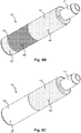
- Fig. 6 shows a spatial representation of an embodiment of the entire calibration unit 1 according to the invention as a plug in the assembled state.
- the housing 2 with the cover 8.
- a thread is further formed by which the calibration unit 1 is screwed to a connection port of the network analyzer to be calibrated.
- the first segment 10 of the connecting element 9 can be seen.
- inner conductor 15 is formed in between, provided with a contact plug 17 inner conductor 15 is formed.
- a housing cap 60 is mounted on the side facing away from the connector of the housing 2.
- FIG. 6 shown embodiment of the entire calibration unit 1 according to the invention are also designed as a socket.
- the inner conductor 15 is replaced by a contact socket 43.
- the union 8 is eliminated and the housing 2 receives an additional thread.
- Fig. 7 shows a sectional spatial representation of an embodiment of the calibration unit 1 according to the invention along the longitudinal axis 20.
- the cut inner conductor 15 is not shown hatched. Shown are the union 8 with its thread, the snap ring 7, the groove 6 and the housing 2. In the housing 2, the different Bohrradien 4 and 5 are clearly visible.
- the two-part inner conductor 15 is centered in the opening third formed of the housing 2 and firmly clamped to the connecting element 9 and / or soldered and / or glued.
- the connecting element 9 is glued with its hood-shaped first segment 10 fixed to the housing 2 and / or soldered.
- Fig. 8 shows the amount of the scattering parameter S11 in a logarithmic representation, ie the reflection loss over the frequency for an embodiment of the calibration unit according to the invention 1.
- the calibration 1 represents in this embodiment, the calibration standard conclusion. It can be seen that the reflection loss in the frequency range from 20 MHz up to 110 GHz takes a maximum value of -30 dB, for example.
- the frequency is plotted on the abscissa linearly from 20 MHz to 110 GHz.
- Termination this is a very good value, which ensures a safer distinction, ie a large dynamic range, between the calibration standard completion and the calibration standards idle and short circuit.
- Fig. 9 shows a flowchart of the method for the production of the calibration unit 1 according to the invention for the embodiment of a conclusion.
- the method steps S 5 to S 8 or S 6 to S 7 are preferably omitted.
- a prefabricated forming die 21 consisting of a base material, preferably of aluminum, is galvanized in a galvanization process, preferably with a gold layer having an adjustable wall thickness.
- the forming punch 21 is also a negative mold of the connecting element 9.
- a thin layer which preferably consists of gold, can be applied to the forming punch 21 by sputtering.
- a second method step S 2 the forming punch 21 is etched away or the connecting element 9 produced by the plating process is pulled off the forming punch 21.
- a third method step S 3 the inner conductor 15 or only a first sub-segment 15 1 is produced in a turning process from a possibly hard metal.
- a very good conductive cover layer is applied to the inner conductor 15 or only a first sub-segment 15 1 by electroplating and / or sputtering.
- the conductive covering layer is preferably a gold layer.
- a thin-film resistor or a thick-film resistor is applied to the second sub-segment 15 2 of the inner conductor 15.
- the second sub-segment 15 2 of the inner conductor 15 is preferably coated with a very good electrically conductive material, such as gold.
- the thin-film resistor or the thick-film resistor of the partial segment 15 2 is formed in a seventh method step S 7 the desired value of eg exactly 50 ohms trimmed with the help of a laser.
- the second sub-segment 15 2 of the inner conductor 15 is electrically conductively soldered and / or glued to a first sub-segment 15 1 of the inner conductor 15.
- both the one-piece inner conductor 15 and the multi-part inner conductor 15 with its first segment 15 1 and its second segment 15 2 are inserted into the connecting element 9 such that the inner conductor 15 is centered in the connecting element 9 and with its end facing away from the connector firmly soldered to the connecting element 9 and / or glued and / or jammed.
- the inner conductor 15 is inserted into the connecting element 9 so far that only the contact plug 17 protrudes from the connecting element 9 or the contact bush 43 is flush with the connecting element 9.
- a tenth method step S 10 the connecting element 9 is inserted into an opening 3 of the housing 2 of the calibration unit 1.
- step S 11 the connecting element 9 is soldered and / or glued electrically conductively to the housing at its first segment 10.
- the calibration unit 1 is suitable for all coaxial plug connections and for all types of measuring devices which have coaxial connection gates. By shrinking In terms of dimensions, the calibration unit can also be used for frequencies above 110 GHz.
- the calibration unit 1 can be designed both as a plug and as a socket.
- the inner conductor 15 has a contact socket 43. In this case, eliminates the cap 8, the groove 6 and the snap ring 7 on the calibration unit 1 and the housing 2 receives an additional thread.
Landscapes
- Physics & Mathematics (AREA)
- General Physics & Mathematics (AREA)
- Measurement Of Resistance Or Impedance (AREA)
Description
- Die Erfindung betrifft eine Kalibriereinheit für ein elektronisches Messgerät, insbesondere für einen Netzwerkanalysator.
- Netzwerkanalysatoren, die zum Bestimmen von Streuparametern von angeschlossenen Messobjekten, wie z.B. von Filtern, Verstärkern und Dämpfungsgliedern dienen, decken einen weiten Frequenzbereich ab und erreichen immer höhere obere Grenzfrequenzen. Über spezielle Aufwärtsmischstufen können die Streuparameter von Messobjekten z.B. im W-Band (75 GHz bis 110 GHz) ermittelt werden. Die einzelnen Komponenten eines Netzwerkanalysators sind dabei selbst fehlerbehaftet und weisen einen Frequenz- und Phasengang auf, der insbesondere bei hohen Frequenzen dazu führt, dass keine genauen Aussagen vom Messobjekt mehr möglich sind. Eine Kalibrierung des Netzwerkanalysators erlaubt dabei diese Systemfehler zu kompensieren, wodurch die Messgenauigkeit stark erhöht wird.
- Eine solche Kalibrierung erfolgt dadurch, dass nacheinander verschiedene Kalibrierstandards mit bekannten elektrischen Eigenschaften an den Messtoren angeschlossen werden und die Messwerte ermittelt werden. Bekannte Kalibrierstandards sind Leerlauf (engl. open), Kurzschluss (engl. short), Abschluss (engl. match) und Durchverbindung (engl. through). Dabei muss z.B. der Kalibrierstandard Abschluss über einen möglichst weiten Frequenzbereich eine möglichst hohe Signaldämpfung erreichen, so dass eine gute Unterscheidbarkeit z.B. zwischen dem Kalibrierstandard Abschluss von dem Kalibrierstandard Kurzschluss gewährleistet ist. Die Kalibrierstandards Leerlauf, Kurschluss und Abschluss liegen dabei als koaxiale Steckverbinder vor, die nacheinander auf die einzelnen koaxialen Messtore des Netzwerkanalysators geschraubt werden. Um Signale mit Frequenzen bis hin zu 110 GHz über eine koaxiale Verbindung übertragen zu können, werden koaxiale Leitungen verwendet, deren Außenleiterdurchmesser 1 mm und deren Innenleiterdurchmesser 0,434 mm betragen. Die als koaxiale Steckverbinder ausgeführten Kalibrierstandards müssen daher entsprechend filigran und gleichzeitig mechanisch stabil gefertigt sein, denn bereits Abweichungen von 0,005 mm im Außenleiterdurchmesser führen dazu, dass sich der Wellenwiderstand um ca. 0,7 Ohm ändert, wodurch keine hoch genauen Messungen mehr möglich sind.
- Aus der
US 5,047,737 A ist ein Abschluss für ein koaxiales Leitungssystem bekannt. Ein Innenleiter besitzt eine Nut, welche zur Aufnahme eines Substrats dient. Das Substrat ist mit einem Dünnschichtwiderstand überzogen, der mit Hilfe einer Lötverbindung mit dem Innenleiter kontaktiert wird. Der Dünnschichtwiderstand verbindet den Innenleiter mit dem Gehäuse. Die Bohrung innerhalb des Gehäuses ist dabei zum Ende hin getapert. Nachteilig an derUS 5,047,737 A ist, dass der Übergang vom Innenleiter auf das Substrat eine nicht unerhebliche Störung des elektromagnetischen Feldes darstellt und damit die Effizienz des Dämpfungsglieds reduziert. - Aus der
WO2006/021280 ist ein koaxialer Kalibrierstandard bekannt. - Es ist daher die Aufgabe der Erfindung eine Kalibriereinheit, die einerseits mechanisch stabil ist und andererseits auch bei sehr hohen Frequenzen optimale Eigenschaften erzielt, und ein entsprechendes Herstellungsverfahren zu schaffen.
- Die Aufgabe wird bezüglich der Kalibriereinheit durch die Merkmale des Anspruchs 1 und bezüglich des Verfahrens durch die Merkmale des Anspruchs 12 gelöst. In den Unteransprüchen sind vorteilhafte Weiterbildungen der erfindungsgemäßen Kalibriereinheit und des erfindungsgemäßen Verfahrens angegeben.
- Die erfindungsgemäße Kalibriereinheit für ein Messgerät zum Verbinden mit einer koaxial ausgeführten Steckverbindung weist ein Gehäuse und einen Innenleiter auf, wobei der Innenleiter zentriert innerhalb einer Öffnung des Gehäuses ausgebildet ist. Die Kalibriereinheit weist weiterhin ein Verbindungselement auf, wobei das Verbindungselement in die Öffnung des Gehäuses einführbar ist und den Innenleiter aufnimmt und wobei das Verbindungselement elastisch ausgeführt ist und den Innenleiter gegenüber dem Gehäuse abstützt.
- Besonders vorteilhaft ist es, dass ein elastisches Verbindungselement in die Öffnung des Gehäuses der Kalibriereinheit einführbar ist und den Innenleiter aufnimmt. Dadurch wird erreicht, dass der Innenleiter besonders gut zentriert ist und immer denselben Abstand zum Außenleiter aufweist, so dass sich der Wellenwiderstand der Kalibrierschaltung über den Frequenzbereich kaum ändert. Durch die elastische Ausbildung des Verbindungselements ist sichergestellt, dass die mechanische Integrität der Kalibriereinheit durch mehrfaches Verschrauben mit der zu kalibrierenden Messeinheit nicht beeinträchtigt ist, auch wenn die Kalibriereinheit nicht auf einem Schlitten befestigt einzig in horizontaler Achse auf die zu kalibrierende Messeinheit zu bewegt wird. Das elastische Verbindungselement dämpft auch kleinere Erschütterungen, die z.B. durch das versehentliche Fallenlassen der Kalibriereinheit entstehen.
- In einem ersten Verfahrensschritt des erfindungsgemäßen Verfahrens zur Herstellung der Kalibriereinheit wird ein Formstempel, welcher eine Negativform eines Verbindungselements hat, galvanisiert, so dass dabei das Verbindungselement entsteht. In einem zweiten Verfahrensschritt wird das galvanisierte Verbindungselement durch Wegätzen des Formstempels oder durch Abziehen des Verbindungselements von dem Formstempel herausgelöst.
- Es ist besonders vorteilhaft, dass bei dem erfindungsgemäßen Verfahren das elastische Verbindungselement durch einen Galvanisierungsprozess hergestellt wird, weil dadurch die Schichtdicke und damit auch die Federrate sehr genau den Erfordernissen entsprechend eingestellt werden kann. Weiterhin ist es von Vorteil, dass der Formstempel durch Ätzten von dem Verbindungselement getrennt wird, weil dadurch das Verbindungselement in seiner Struktur selbst erhalten bleibt.
- Ein weiterer Vorteil der erfindungsgemäßen Kalibriereinheit besteht, wenn das Verbindungselement trichterförmig ausgebildet ist und mehrere zusammenhängende Teilsegmente umfasst. Die trichterförmige Ausbildung mit einem sich in seinem Durchmesser verändernden Segment, sorgt dafür, dass die Kalibriereinheit über einen sehr weiten Frequenzbereich optimale Eigenschaften aufweist. Die verschiedenen Teilsegmente des Verbindungselements sind unterschiedlich ausgebildet und dienen z.B. der Befestigung des Verbindungselements am Gehäuse oder zur Aufnahme des Innenleiters durch das Verbindungselement.
- Außerdem besteht ein Vorteil der erfindungsgemäßen Kalibriereinheit, wenn ein erstes Teilsegment des Verbindungselements als Flansch oder Haube ausgebildet ist und mit dem Gehäuse elektrisch leitend verklebt und/oder verpresst und/oder verlötet ist. Ein als Flansch oder Haube ausgebildetes erstes Teilsegment des Verbindungselements, welches sich über die Öffnung des Gehäuses legt, stellt sicher, dass das Verbindungselement nicht innerhalb der Öffnung des Gehäuses verkantet, sondern immer in optimaler Ausrichtung montiert werden kann. Dadurch, dass das Verbindungselement mit dem Gehäuse verklebt und/oder verpresst und/oder verlötet wird, ist sichergestellt, dass sich das Verbindungselement auch im Laufe der Zeit nicht löst und somit der vom Verbindungselement aufgenommene Innenleiter dauerhaft in seiner Position fixiert ist.
- Schlussendlich besteht ein Vorteil der erfindungsgemäßen Kalibriereinheit, wenn der Innenleiter im Falle der Lastzustände Leerlauf und Abschluss aus zumindest zwei Teilsegmenten besteht, wobei ein zweites Teilsegment aus einem Dielektrikum besteht, welches im Falle des Lastzustands Abschluss abschnittsweise mit einem Dünnschichtwiderstand oder Dickschichtwiderstand und einem elektrisch leitfähigen Material überzogen ist. Dies erlaubt, dass die Kalibriereinheit einerseits die Kalibrierstandards Kurzschluss und Leerlauf abdeckt und andererseits auch mittels des Dünnschichtwiderstands oder Dickschichtwiderstands für den Kalibrierstandard Abschluss verwendbar ist. Der Dünnschichtwiderstand oder der Dickschichtwiderstand ist für gewöhnlich derart gewählt, dass die Kalibriereinheit einen Widerstand von 50 Ohm über einen möglichst weiten Frequenzbereich bis hin zu 110 GHz möglichst genau erreicht.
- Bei dem erfindungsgemäßen Verfahren zur Herstellung der Kalibriereinheit besteht weiterhin ein Vorteil, wenn der Innenleiter oder ein erstes Segment des Innenleiters in einem Drehprozess hergestellt und mit einem sehr gut leitfähigen Material galvanisiert und/oder besputtert wird. Anhand dieser weiteren Verfahrensschritte kann der Innenleiter sehr genau hergestellt werden, so dass sich der Wellenwiderstand nicht ändert. Drehprozesse erlauben eine Genauigkeit von wenigen Mikrometern.
- Ferner besteht bei dem erfindungsgemäßen Verfahren zur Herstellung der Kalibriereinheit ein Vorteil, wenn ein zweites Segment des Innenleiters mit dieelektrischen Eigenschaften durch einen Pressprozess und/oder Sinterprozess und/oder Drehprozess hergestellt wird und wenn auf das zweite Segment abschnittsweise ein Dünnschichtwiderstand oder Dickschichtwiderstand und eine elektrisch leitfähige Schicht aufgetragen wird und wenn anschließend der Dünnschichtwiderstand oder der Dickschichtwiderstand mittels eines Lasers getrimmt werden und wenn das zweite Segment des Innenleiters mittels eines Lötprozesses und/oder Klebeprozesses mit einem ersten Segment des Innenleiters verbunden wird. Dies erlaubt die Herstellung einer Kalibriereinheit für den Kalibrierstandard Abschluss, wobei der Dünnschichtwiderstand derart gewählt wird, dass die Kalibriereinheit möglichst genau einen Widerstandstand von z.B. 50 Ohm darstellt.
- Schlussendlich besteht bei dem erfindungsgemäßen Verfahren zur Herstellung einer Kalibriereinheit ein Vorteil, wenn der Innenleiter oder das erste Teilsegment und das zweite Teilsegment des Innenleiters in das Verbindungselement geschoben wird, so dass anschließend das Verbindungselement in die Öffnung des Gehäuses eingeführt und mit dem Gehäuse verlötet oder verklebt werden kann. Eine derartige Ausgestaltung des Verbindungselements erlaubt eine sehr einfache Montage, wobei das Verbindungselement dabei auch für Kalibriereinheiten verwendet werden kann, die die Kalibrierstandards Leerlauf und Kurzschluss abdecken. Beim Kalibrierstandard Leerlauf wird das zweite Segment des Innenleiters nicht mit dem Dünnschichtwiderstand beschichtet und beim Kalibrierstandard Kurzschluss besteht das zweite Segment des Innenleiters aus einem Metall oder ist mit einer metallischen Schicht überzogen.
- Verschiedene Ausführungsbeispiele der Erfindung werden nachfolgend unter Bezugnahme auf die Zeichnung beispielhaft beschrieben. Gleiche Gegenstände weisen dieselben Bezugszeichen auf. Die entsprechenden Figuren der Zeichnung zeigen im Einzelnen:
- Fig. 1
- einen Schnitt entlang einer Längsachse durch ein erfindungsgemäßes Ausführungsbeispiel der Kalibriereinheit;
- Fig. 2A
- einen Schnitt entlang der Längsachse durch ein erfindungsgemäßes Ausführungsbeispiel des Verbindungselements;
- Fig. 2B
- einen Schnitt entlang der Längsachse durch einen Formstempel eines Ausführungsbeispiels des erfindungsgemäßen Verbindungselements;
- Fig. 3
- einen Schnitt entlang der Längsachse durch ein Ausführungsbeispiel des erfindungsgemäßen Verbindungselements in einer perspektivischen Ansicht;
- Fig. 4A
- eine räumliche Darstellung eines Ausführungsbeispiels eines erfindungsgemäßen Innenleiters mit einem Kontaktstecker;
- Fig. 4B
- eine räumliche Darstellung eines Ausführungsbeispiels eines erfindungsgemäßen Innenleiters mit einer Kontaktbuchse;
- Fig. 5A
- eine räumliche Darstellung eines Ausführungsbeispiels eines erfindungsgemäßen Innenleiters, wie er für den Kalibrierstandard Kurzschluss verwendet werden kann;
- Fig. 5B
- eine räumliche Darstellung eines Ausführungsbeispiels eines erfindungsgemäßen Innenleiters, wie er für den Kalibrierstandard Abschluss verwendet werden kann;
- Fig. 5C
- eine räumliche Darstellung eines Ausführungsbeispiels eines erfindungsgemäßen Innenleiters, wie er für den Kalibrierstandard Leerlauf verwendet werden kann;
- Fig. 6
- eine räumliche Darstellung eines Ausführungsbeispiels der erfindungsgemäßen Kalibriereinheit im montierten Zustand;
- Fig. 7
- eine geschnittene räumliche Darstellung eines Ausführungsbeispiels der erfindungsgemäßen Kalibriereinheit entlang der Längsachse;
- Fig. 8
- den S11-Parameter über die Frequenz aufgetragen für ein Ausführungsbeispiel der erfindungsgemäßen Kalibriereinheit; und
- Fig. 9
- ein Ausführungsbeispiel für ein Flussdiagramm für die Herstellung der erfindungsgemäßen Kalibriereinheit.
-
Fig. 1 zeigt einen Schnitt entlang einer Längsachse 20 durch ein erfindungsgemäßes Ausführungsbeispiel der Kalibriereinheit 1. Die Kalibriereinheit 1 wird mit einem Messgerät, bei welchem es sich bevorzugt um einen Netzwerkanalysator handelt, verbunden. Dabei ist die Kalibriereinheit 1 als koaxial ausgeführte Steckverbindung ausgebildet und kann bei einem Frequenzbereich von bis zu 110 GHz einen Außenleiter mit einem Außenleiterdurchmesser von 1 mm aufnehmen. Die Kalibriereinheit 1 umfasst ein Gehäuse 2, welches elektrisch leitfähig ist oder zumindest mit einer sehr gut elektrisch leitfähigen Schicht überzogen ist. Bevorzugt wird das Gehäuse 2 mit einer Goldschicht in einem Galvanisierungsprozess überzogen. Abhängig von der Gehäuseform kann das Gehäuse 2 auch in einem Sputterprozess mit der leitfähigen Schicht überzogen werden. Das Gehäuse 2 ist in dem erfindungsgemäßen Ausführungsbeispiel ausFig. 1 als Hohlzylinder ausgebildet und weist eine Öffnung 3 auf. Die Öffnung 3 entsteht dabei bevorzugt durch einen Bohrprozess, wobei ein erster Bohrradius 4 am aufnahmeseitigen Ende des Gehäuses 2 bevorzugt kleiner gewählt ist, als ein zweiter Bohrradius 5 an dem aufnahmeseitigen Ende entgegengesetzten zweiten Ende des Gehäuses 2. Der Außendurchmesser des Gehäuses 2 ist am aufnahmeseitigen Ende ebenfalls kleiner als an dem zweiten Ende des Gehäuses 2. - An dem zweiten Ende des Gehäuses 2 ist eine Nut 6 ausgebildet, die in einem Drehprozess herstellbar ist. In die Nut 6 wird ein Sprengring 7 eingeführt, an dem ein Überwurf 8 befestigt ist, so dass der Überwurf 8 beweglich am Gehäuse 2 gehalten wird. Der Überwurf 8 weist an dem anschlussseitigen Ende des Gehäuses 2 ein Gewinde auf, mit dessen Hilfe die Kalibriereinheit 1 fest an einem Anschlusstor des Netzwerkanalysators verschraubbar ist. Weiterhin weist die Kalibriereinheit 1 ein Verbindungselement 9 auf, wobei das Verbindungselement 9 bevorzugt in die Öffnung 3 des anschlussseitigen Endes des Gehäuses 2 einführbar ist. Das Verbindungselement 9 ist bevorzugt trichterförmig ausgebildet und umfasst mehrere zusammenhängende Teilsegmente. Ein erstes Teilsegment 10 des Verbindungselements 9 ist als Flansch oder Haube ausgebildet und mit dem anschlussseitigen Ende des Gehäuses 2 verklebt und/oder verpresst und/oder verlötet. Weil ein Radius des ersten Teilsegments 10 des Verbindungelements 9 größer ist, als der Radius 4 der ersten Bohrung, ist sichergestellt, dass das Verbindungselements 9 bei der Montage nicht durch die Öffnung 3 des Gehäuses 2 hindurch fällt. Eine das Gehäuse 2 teilweise umgreifende Haubenform des ersten Teilsegments 10 des Verbindungselements 9 bewirkt, dass das Verbindungselement 9 teilweise in axialer Richtung fixiert ist, bis es verklebt und/oder verpresst und/oder verlötet ist und sich selbstständig zentriert.
- Ein zweites Teilsegment 11 des Verbindungselements 9 besitzt einen Innendurchmesser, der dem Innendurchmesser des Außenleiters der anzuschließenden Steckverbindung plus zweimal der Wandstärke des Verbindungselements 9 entspricht, wobei der Radius 4 der ersten Bohrung bevorzugt derart gewählt ist, dass das zweite Teilsegment 11 formschlüssig an einer Innenfläche 12 des Gehäuses 2 anliegt.
- Ein drittes Teilsegment 13 des Verbindungselements 9 ist verengend, z.B. konisch ausgebildet, so dass sich das Verbindungselement 9 dadurch in seinem Durchmesser verjüngt. Die sich verengende Form des dritten Teilsegments 13 des Verbindungselements 9 bewirkt, dass das Verbindungselement 9 einerseits elastische Eigenschaften aufweist und anderseits eine optimale Anpassung bis hin zu Frequenzen von 110 GHz und mehr ermöglicht. Je nach Formgebung des Gehäuses 2 sind unter Umständen auch andere mathematisch basierte Formgebungen für das dritte Teilsegment 13 denkbar, wenn sie das Reflexionsverhalten günstig beeinflussen.
- Ein viertes Teilsegment 14 des Verbindungselements 9 dient dabei als Aufnahmeelement für einen Innenleiter 15. Der Durchmesser dieses vierten Teilsegments 14 ist dabei so gewählt, dass der Innenleiter 15 in dieses einführbar ist. Das Verbindungselement 9 besteht aus einem sehr gut leitfähigen Material, bevorzugt aus Gold. Auf den Herstellungsprozess des Verbindungselements 9 wird im Weiteren noch gesondert eingegangen.
- Der Innenleiter 15 ist über das Verbindungselement 9 zentriert innerhalb der Öffnung 3 des Gehäuses 2 ausgebildet. Der Innenleiter 15 der Kalibriereinheit 1 ist, je nachdem, ob die Kalibriereinheit 1 die Kalibrierstandards Leerlauf oder Kurzschluss oder Abschluss darstellt, einteilig oder mehrteilig ausgebildet.
- Soll die Kalibriereinheit 1 den Kalibrierstandard Kurzschluss erfüllen, dann ist der Innenleiter 15 bevorzugt aus einem Metall einteilig ausgebildet, wobei die Oberfläche des Innenleiters 15 bevorzugt mit einem sehr gut leitfähigen Material, bevorzugt mit Gold, überzogen ist.
-
Fig. 1 zeigt eine zweiteilige Ausbildung des Innenleiters 15, wie er für die Kalibrierstandards Leerlauf und Abschluss aufgebaut sein kann. Der Innenleiter 15 ist aus zwei Teilsegmenten aufgebaut. Ein erstes Teilsegment 151 des Innenleiters 15 ist entweder als Kontaktstecker 17 oder als Kontaktbuchse 43 ausgebildet und kontaktiert ein Anschlusstor des zu kalibrierenden Netzwerkanalysators direkt oder indirekt über ein koaxiales Verbindungskabel. Zu erkennen ist, dass in dem Ausführungsbeispiel ausFig. 1 das erste Teilsegment 151 des Innenleiters 15 als Kontaktstecker 17 ausgebildet ist. Der Kontaktstecker 17 des ersten Teilsegments 151 des Innenleiters 15 weist dabei einen kleineren Durchmesser auf, als der Innenleiter 15 selbst. Das erste Teilsegment 151 des Innenleiters 15 weist an dem, dem Kontaktstecker 17 abgewandtem Ende, eine Bohrung 19 auf, in die das zweite Teilsegment 152 des Innenleiters 15 gesteckt ist. Das zweite Teilsegment 152 des Innenleiters 15 ist elektrisch leitend mit dem ersten Teilsegment 151 des Innenleiters 15 verklebt und/oder verlötet. Der Durchmesser des Innenleiters 15 beträgt für den Fall, dass es sich bei der Steckverbindung der Kalibriereinheit 1 um eine koaxiale 1mm-Steckverbindung handelt, die für Frequenzen bis 110 GHz geeignet ist, 0,434 mm. - Das zweite Teilsegment 152 besteht aus einem Dielektrikum mit einer möglichst niedrigen dielektrischen Leitfähigkeit εr und einer hohen Biegefestigkeit, so dass der Innenleiter 15 auch mechanischen Beanspruchungen standhält. Zirkoniumoxid weist im Gegensatz zu Aluminiumoxid zwar eine höhere Biegefestigkeit auf, allerdings ist die Permittivität εr recht hoch. Ein guter Kompromiss stellt Siliziumnitrid (Si3N4) dar, welches gesintert oder bevorzugt gehippt eine sehr hohe Biegefestigkeit bei gleichzeitig niedriger Permittivität εr aufweist.
- Für den Fall, dass die Kalibriereinheit 1 den Kalibrierstandard Abschluss bildet, ist das zweite Teilsegment 152 des Innenleiters 15, welches als Absorber dient, mit einem Dünnschichtwiderstand oder Dickschichtwiderstand überzogen. Als Material für den Dünnschichtwiderstand eignet sich z.B. eine Nickel-Chrom-Legierung. Das zweite Teilsegment 152 des Innenleiters 15 ist dabei ganz oder teilweise mit dem Dünnschichtwiderstand oder dem Dickschichtwiderstand überzogen. An einer Kontaktstelle zwischen dem vierten Teilsegment 14 des Verbindungselements 9 und dem zweiten Teilsegment 152 des Innenleiters 15 ist das zweite Teilsegment 152 des Innenleiters 15 bevorzugt mit einem elektrisch sehr gut leitfähigen Material, wie z.B. Gold, überzogen.
- Für den Fall, dass die Kalibriereinheit 1 den Kalibrierstandard Leerlauf bildet, kann z.B. auf den Überzug des zweiten Teilsegments 152 des Innenleiters 15 mit dem Dünnschichtwiderstand oder dem Dickschichtwiderstand ganz verzichtet werden. Das zweite Teilsegment 152 des Innenleiters 15 wird mit dem Verbindungselement 9, bzw. mit dem vierten Teilsegment 14 des Verbindungselements 9 verklebt und/oder verlötet und/oder verklemmt.
- Der Innenleiter 15 wird derart weit in die Öffnung 3 des Verbindungselements 9 hineingeschoben, bis einzig der Kontaktstecker 17 aus der Öffnung 3 des Verbindungselements 9 hervorsteht. Anstelle eines Kontaktsteckers 17 kann der Innenleiter 15 an seiner nicht mit dem Verbindungselement 9 verbundenen Seite auch als
- Kontaktbuchse 43 ausgebildet sein, wobei in diesem Fall die Kontaktbuchse 43 mit der Öffnung des Verbindungselements 9 bündig abschließt. Das Verbindungselement 9 besteht dabei aus einem elektrisch leitfähigen Material und verbindet den Innenleiter 15 elektrisch leitend mit dem Gehäuse 2.
-
Fig. 2A zeigt einen Schnitt entlang der Längsachse 20 durch ein erfindungsgemäßes Ausführungsbeispiel des Verbindungselements 9. Gut zu erkennen sind die vier Teilsegmente 10, 11, 13, 14 die nahtlos miteinander verbunden sind und das Verbindungselement 9 bilden. Wie bereits erläutert, erlaubt das dritte Segment 13, dass der durch das Verbindungselement 9 aufgenommene Innenleiter 15 gegenüber dem Gehäuse elastisch abgestützt wird. Dadurch ist sichergestellt, dass der Innenleiter 15 auch bei mehrmaligem An- und Abschrauben der Kalibriereinheit 1 an ein Anschlusstor des Netzwerkanalysators oder an eine koaxiale Verbindungsleitung zum Netzwerkanalysator stets zentriert innerhalb der Öffnung 3 des Gehäuses 2 ausgerichtet ist, so dass die gewünschten Eigenschaften der Kalibriereinheit 1 auch für hohe Frequenzen zuverlässig erhalten bleiben. Dies gilt auch für den Fall, dass die Kalibriereinheit 1 versehentlich zu Boden fällt.Fig. 2B zeigt einen Schnitt entlang der Längsachse 20 durch einen Formstempel 21 eines Ausführungsbeispiels des erfindungsgemäßen Verbindungselements 9. Damit die Kalibriereinheit 1 die verschiedenen Kalibrierstandards für Frequenzen bis zu 110 GHz optimal abbildet, muss das Verbindungselement 9, welches einerseits für die optimale Anpassung sorgt und andererseits der Kalibriereinheit 1 eine ausreichende mechanische Stabilität gibt, sehr genau gefertigt werden. Hierzu wird der Formstempel 21 bevorzugt aus Aluminium gedreht. Dieser Formstempel 21 ist inFig. 2B zu erkennen. Anschließend wird der Formstempel 21 in einem Galvanisierungsverfahren mit einem sehr gut elektrisch leitfähigen Material, wie z.B. Gold, überzogen. Die Wandstärke des Verbindungselements 9 kann dabei beliebig im Bereich einiger zig Mikrometer sehr präzise eingestellt werden. Die Wandstärke des Verbindungselements 9 wird dabei so gewählt, dass der Innenleiter 15 der Kalibriereinheit 1 im Kleinen elastisch beweglich ist und dadurch ein Bruch des Innenleiters 15, bzw. des zweiten Teilsegments 152 des Innenleiters 15 vermieden wird. - Sobald die richtige Wandstärke erreicht ist, kann das Verbindungselement 9 von dem Formstempel 21 abgezogen werden. Bevorzugt wird allerdings der z.B. aus Aluminium bestehende Formstempel 21 weggeätzt, so dass einzig das Verbindungselement 9 erhalten bleibt. Dies kann z.B. durch Verwendung von Natronlauge erreicht werden. Dadurch ist sichergestellt, dass die gewünschte Form des Verbindungselements 9 erhalten bleibt. Durch die bevorzugt konische Form des dritten Teilsegments 13 wird erreicht, dass eine Kalibriereinheit 1, die den Kalibrierstandard Abschluss bildet, über einen weiten Frequenzbereich ein optimales Dämpfungsverhalten zeigt. Die Vertiefung 22 am Ende des Formstempels 21 sorgt dafür, dass im vierten Teilsegment 14 des Verbindungselements ein nach innen verlaufender Kegel entsteht. Dieser dient als Zentrierhilfe für eine Bohrung, um nach dem Galvanisierungsschritt den späteren Ätzprozess zu beschleunigen.
-
Fig. 3 zeigt einen Schnitt entlang der Längsachse 20 durch ein Ausführungsbeispiel des erfindungsgemäßen Verbindungselements 9 in einer perspektivischen Ansicht. Das erste Teilsegment 10 des Verbindungselements 9 weist dabei eine Haubenform wie inFig. 1 auf. Eine planare flanschförmige Ausbildung ist aber ebenfalls möglich. Außerdem sind die weiteren Teilsegmente 11, 13, 14 gezeigt, wobei der Innenleiter 15 mit dem vierten Teilsegment 14 verklebt und/oder verlötet und/oder verklemmt ist. -
Fig. 4A zeigt eine räumliche Darstellung eines Ausführungsbeispiels eines erfindungsgemäßen Innenleiters 15 mit seinem Kontaktstecker 17. Bei dem dargestellten Innenleiter 15 kann es sich auch nur um das erste Segment 151 des Innenleiters 15 ausFig. 1 handeln. Der Innenleiter 15 und sein Kontaktstecker 17 werden in einem Drehprozess hergestellt und anschließend durch Sputtern oder Galvanisieren mit einer sehr gut elektrisch leitfähigen Schicht überzogen. Der Sputter- oder Galvanisierungsprozess wird dabei so eingestellt, dass sich der gewünschte Durchmesser für den Innenleiter 15 ergibt. -
Fig. 4B zeigt eine räumliche Darstellung eines Ausführungsbeispiels eines erfindungsgemäßen Innenleiters 15 mit einer Kontaktbuchse 43, bei dem es sich ebenfalls nur um das erste Segment 151 des Innenleiters 15 ausFig. 1 handeln kann und der ebenfalls bevorzugt in einem Drehprozess hergestellt wird. Anschließend wird in einem Bohrprozess ein Bohrloch 41 in den Innenleiter 15 gebohrt und in einem anschließenden Fräsprozess zumindest ein Längsschlitz 42 in die Kontaktbuchse 43 gefräst. Schließlich wird die Kontaktbuchse 43, wie inFig. 4B gezeigt, konisch zusammengepresst, so dass sich die Kontaktbuchse 43 bei Kontaktierung mit einem Steckkontakt wie inFig. 4A derart weitet, dass der Innenleiter 15 einen Durchmesser von 0,434 mm aufweist. Der mit der Kontaktbuchse 43 versehene geschlitzte und in seinem Durchmesser etwas verkleinerte Innenleiter 15 wird, wie auch der mit einem Steckkontakt versehene Innenleiter 15, in einem Sputter- oder Galvanisierungsprozess mit einer sehr gut elektrisch leitfähigen Schicht überzogen, wobei der Prozess so eingestellt ist, dass sich der gewünschte Durchmesser des Innenleiters 15 ergibt. -
Fig. 5A zeigt eine räumliche Darstellung eines Ausführungsbeispiels eines erfindungsgemäßen Innenleiters 15, wie er z.B. für den Kalibrierstandard Kurzschluss verwendet werden kann. Der Innenleiter 15 besteht in diesem Ausführungsbeispiel aus einem ersten Teilsegment 151 und einem zweiten Teilsegment 152, deren Oberflächen 44 und 45 jeweils mit einer sehr gut elektrisch leitfähigen Schicht überzogen sind. Bevorzugt ist der Innenleiter 15 für den Kalibrierstandard Kurzschluss allerdings einteilig ausgebildet, so dass sich keinerlei Störstelle zwischen dem ersten Teilsegment 151 und dem zweiten Teilsegment 152 ausbilden kann. -
Fig. 5B zeigt eine räumliche Darstellung eines Ausführungsbeispiels des erfindungsgemäßen Innenleiters 15, wie er für den Kalibrierstandard Abschluss verwendet werden kann. Der Innenleiter 15 ist dabei zweiteilig ausbildet und weist ein erstes Teilsegment 151 und ein zweites Teilsegment 152 auf. Zumindest die Oberfläche 44 des ersten Teilsegments 151 ist dabei mit einem elektrisch sehr gut leitenden Material, bevorzugt Gold, beschichtet. Das zweite Teilsegment 152, welches aus einem Dielektrikum besteht, ist bevorzugt an seiner Oberfläche 47, die elektrisch leitend mit dem vierten Teilsegment 14 des Verbindungselements 9 verbunden ist, mit einer elektrisch leitfähigen Schicht, z.B. aus Gold versehen. Die Oberfläche 47 nimmt dabei nur einen Teil der Oberfläche des zweiten Teilsegments 152 des Innenleiters 15 ein. Die restliche Oberfläche 46 des zweiten Teilsegments 152 des Innenleiters 15 ist mit einem Dünnschichtwiderstand oder einem Dickschichtwiderstand überzogen, dessen Dicke derart gewählt ist, dass der Innenleiter 15 mit seinem ersten Teilsegment 151 und seinem zweiten Teilsegment 152 und dem Verbindungselement 9 sowie dem Gehäuse 2 einen Widerstandswert z.B. etwas unterhalb von 50 Ohm erreicht. Durch einen Trimmvorgang mit Hilfe eines Lasers wird dann der gewünschte Widerstandswert von z.B. exakt 50 Ohm eingestellt. -
Fig. 5C zeigt eine räumliche Darstellung eines Ausführungsbeispiels eines erfindungsgemäßen Innenleiters 15, wie er für den Kalibrierstandard Leerlauf verwendet werden kann. Der Innenleiter 15 ist mit seinem ersten Teilsegment 151 und seinem zweiten Teilsegment 152 dabei zweiteilig ausgebildet. Das erste Teilsegment 151 des Innenleiters 15 ist dabei zumindest an seiner Oberfläche 44 mit einer elektrisch leitfähigen Schicht überzogen. Das zweite Teilsegment 152 ist bevorzugt an seiner Oberfläche 47, die mechanisch direkt mit dem vierten Teilsegment 14 des Verbindungselements 9 verbunden ist, mit keiner oder mit einer elektrisch nicht leitenden Schicht überzogen. -
Fig. 6 zeigt eine räumliche Darstellung eines Ausführungsbeispiels der gesamten erfindungsgemäßen Kalibriereinheit 1 als Stecker im montierten Zustand. Zu erkennen ist das Gehäuse 2 mit dem Überwurf 8. In dem Überwurf 8 ist ferner noch ein Gewinde ausgebildet, durch welches die Kalibriereinheit 1 mit einem Anschlusstor des zu kalibrierenden Netzwerkanalysators verschraubt wird. Weiterhin ist das erste Segment 10 des Verbindungselements 9 zu erkennen. Dazwischen ist der mit einem Kontaktstecker 17 versehene Innenleiter 15 ausgebildet. Eine Gehäusekappe 60 ist auf der, der Steckverbindung abgewandten Seite des Gehäuses 2, angebracht. Prinzipiell kann das inFig. 6 gezeigte Ausführungsbeispiel der gesamten erfindungsgemäßen Kalibriereinheit 1 auch als Buchse ausgeführt werden. Dazu erhält der Innenleiter 15 eine Kontaktbuchse 43. Ferner entfällt der Überwurf 8 und das Gehäuse 2 erhält ein zusätzliches Gewinde. -
Fig. 7 zeigt eine geschnittene räumliche Darstellung eines Ausführungsbeispiels der erfindungsgemäßen Kalibriereinheit 1 entlang der Längsachse 20. Zur besseren Übersicht ist der geschnittene Innenleiter 15 nicht schraffiert abgebildet. Dargestellt sind der Überwurf 8 mit seinem Gewinde, der Sprengring 7, die Nut 6 und das Gehäuse 2. Bei dem Gehäuse 2 sind die unterschiedlichen Bohrradien 4 und 5 gut erkennbar. Der zweiteilig ausgebildete Innenleiter 15 ist zentriert in der Öffnung 3 des Gehäuses 2 ausgebildet und fest mit dem Verbindungselement 9 verklemmt und/oder verlötet und/oder verklebt. Das Verbindungselement 9 ist mit seinem haubenförmig ausgebildeten ersten Segment 10 fest mit dem Gehäuse 2 verklebt und/oder verlötet. -
Fig. 8 zeigt den Betrag des Streuparameters S11 in logarithmischer Darstellung, also die Reflexionsdämpfung über der Frequenz für ein Ausführungsbeispiel der erfindungsgemäßen Kalibriereinheit 1. Die Kalibrierienheit 1 stellt in diesem Ausführungsbeispiel den Kalibrierstandard Abschluss dar. Zu erkennen ist, dass die Reflexionsdämpfung im Frequenzbereich von 20 MHz bis zu 110 GHz maximal einen Wert von z.B. -30 dB annimmt. Die Frequenz ist auf der Abszisse linear von 20 MHz bis 110 GHz aufgetragen. Für den Kalibrierstandard Abschluss ist dies ein sehr guter Wert, der eine sicherere Unterscheidung, also einen großen Dynamikbereich, zwischen dem Kalibrierstandard Abschluss und den Kalibrierstandards Leerlauf und Kurzschluss gewährleistet. -
Fig. 9 zeigt ein Flussdiagramm des Verfahrens für die Herstellung der erfindungsgemäßen Kalibriereinheit 1 für das Ausführungsbeispiels eines Abschlusses. Für die Ausführungsbeispiele Kurzschluss, bzw. Leerlauf werden die Verfahrensschritte S5 bis S8 bzw. S6 bis S7 bevorzugt ausgelassen. In einem ersten Verfahrensschritt S1 wird ein vorgefertigter Formstempel 21 bestehend aus einem Grundmaterial, bevorzugt aus Aluminium, in einem Galvanisierungsverfahren bevorzugt mit einer Goldschicht mit einstellbarer Wandstärke galvanisiert. Bei dem Formstempel 21 handelt es sich auch um eine Negativform des Verbindungselements 9. Vor dem Galvanisierungsprozess kann auf den Formstempel 21 auch eine dünne Schicht, die bevorzugt aus Gold besteht, durch Sputtern aufgetragen werden. - In einem zweiten Verfahrensschritt S2 wird der Formstempel 21 weggeätzt oder das durch den Galvanisierungsprozess entstandene Verbindungselement 9 von dem Formstempel 21 abgezogen.
- In einem dritten Verfahrensschritt S3 wird der Innenleiter 15 oder nur ein erstes Teilsegment 151 in einem Drehprozess aus einem nach Möglichkeit hartem Metall hergestellt.
- In einem vierten Verfahrensschritt S4 wird eine sehr gut leitfähige Deckschicht auf den Innenleiter 15 oder nur ein erstes Teilsegment 151 durch Galvanisieren und/oder Sputtern aufgetragen. Bevorzugt handelt es sich bei der leitfähigen Deckschicht um eine Goldschicht.
- Für den Fall, dass die Kalibriereinheit 1 die Kalibrierstandards Leerlauf oder Abschluss bilden soll, wird in einem fünften Verfahrensschritt S5 ein zweites Teilsegment 152 des Innenleiters 15, bevorzugt aus einem Dielektrikum, wie z.B. gesintertem oder gehipptem Silizium-Nitrid (Si3N4), hergestellt.
- Für den Fall, dass die Kalibriereinheit 1 den Kalibrierstandard Abschluss bilden soll, wird in einem sechsten Verfahrensschritt S6 ein Dünnschichtwiderstand oder ein Dickschichtwiderstand auf das zweite Teilsegment 152 des Innenleiters 15 aufgetragen. An einer Kontaktstelle zwischen dem vierten Teilsegment 14 des Verbindungselements 9 und dem zweiten Teilsegment 152 des Innenleiters 15 ist das zweite Teilsegment 152 des Innenleiters 15 bevorzugt mit einem elektrisch sehr gut leitfähigen Material, wie z.B. Gold, überzogen.
- Für den Fall, dass die Kalibriereinheit 1 den Kalibrierstandard Abschluss bilden soll, wird in einem siebten Verfahrensschritt S7 der Dünnschichtwiderstand oder der Dickschichtwiderstand des Teilsegments 152 auf den gewünschten Wert von z.B. exakt 50 Ohm mit Hilfe eines Lasers getrimmt.
- Für den Fall, dass die Kalibriereinheit 1 die Kalibrierstandards Leerlauf oder Abschluss bilden soll, wird in einem achten Verfahrensschritt S8 das zweite Teilsegment 152 des Innenleiters 15 mit einem ersten Teilsegment 151 des Innenleiters 15 elektrisch leitend verlötet und/oder verklebt.
- In einem neunten Verfahrensschritt S9 wird sowohl der einteilige ausgebildete Innenleiter 15 als auch der mehrteilig ausgebildete Innenleiter 15 mit seinem ersten Segment 151 und seinem zweiten Segment 152 in das Verbindungselement 9 derart eingeschoben, dass der Innenleiter 15 zentriert in dem Verbindungselement 9 angeordnet ist und mit seinem dem Anschlussstecker abgewandten Ende fest mit dem Verbindungselement 9 verlötet und/oder verklebt und/oder verklemmt ist. Der Innenleiter 15 wird dabei soweit in das Verbindungselement 9 eingeschoben, dass einzig der Kontaktstecker 17 aus dem Verbindungselement 9 hervorsteht oder die Kontaktbuchse 43 bündig mit dem Verbindungselement 9 abschließt.
- In einem zehnten Verfahrensschritt S10 wird das Verbindungselement 9 in eine Öffnung 3 des Gehäuses 2 der Kalibriereinheit 1 eingeführt.
- In einem elften Verfahrensschritt S11 wird das Verbindungelement 9 an seinem ersten Segment 10 mit dem Gehäuse elektrisch leitend verlötet und/oder verklebt.
- Im Rahmen der Erfindung sind alle beschriebenen und/oder gezeichneten Merkmale beliebig miteinander kombinierbar. Die Kalibriereinheit 1 eignet sich für sämtliche koaxiale Steckverbindungen und für alle Arten von Messgeräten die über koaxiale Anschlusstore verfügen. Durch Verkleinern der Abmessungen ist die Kalibriereinheit auch für Frequenzen oberhalb von 110 GHz einsetzbar.
- Die erfindungsgemäße Kalibriereinheit 1 kann sowohl als Stecker und auch als Buchse ausgeführt sein. Bei Ausführung als Buchse weist der Innenleiter 15 eine Kontaktbuchse 43 auf. Dabei entfällt der Überwurf 8, die Nut 6 und der Sprengring 7 an der Kalibriereinheit 1 und das Gehäuse 2 erhält ein zusätzliches Gewinde.
Claims (17)
- Kalibriereinheit (1) für ein Messgerät zum Verbinden mit einer koaxial ausgeführten Steckverbindung, aufweisend ein Gehäuse (2) und einen Innenleiter (15), wobei der Innenleiter (15) zentriert innerhalb einer Öffnung (3) des Gehäuses (2) ausgebildet ist,
wobei die Kalibriereinheit (1) ein Verbindungselement (9) aufweist,
wobei das Verbindungselement (9) in die Öffnung (3) des Gehäuses (2) eingesetzt ist und
wobei das Verbindungselement (9) elastisch ausgebildet ist,
wobei das Verbindungselement (9) den Innenleiter (15) aufnimmt,
wobei das Verbindungselement (9) den Innenleiter (15) gegenüber dem Gehäuse (2) elastisch abstützt,
wobei Verbindungselement (9) trichterförmig ausgebildet ist und mehrere nahtlos zusammenhängende Teilsegmente (10, 11, 13, 14) umfasst,
wobei ein erstes Teilsegment (10) des Verbindungselements (9) als Flansch oder Haube ausgebildet ist und mit dem Gehäuse (2) elektrisch leitend verklebt und/oder verpresst und/oder verlötet ist,
wobei das Gehäuse (2) elektrisch leitfähig ist oder zumindest mit einer elektrisch leitfähigen Schicht überzogen ist und
wobei das Verbindungselement (9) aus einem elektrisch leitfähigen Material besteht. - Kalibriereinheit nach Anspruch 1,
dadurch gekennzeichnet,
dass ein zweites Teilsegment (11) des Verbindungselements (9) einen Innendurchmesser aufweist, der dem Innendurchmesser des Außenleiters der anzuschließenden Steckverbindung entspricht. - Kalibriereinheit nach Anspruch 1 oder 2,
dadurch gekennzeichnet,
dass ein drittes Teilsegment (13) des Verbindungselements (9) verengend, insbesondere konisch ausgebildet ist und das Verbindungselement (9) dadurch in seinem Durchmesser verjüngt. - Kalibriereinheit nach einem der Ansprüche 1 bis 3,
dadurch gekennzeichnet,
dass ein viertes Teilsegment (14) des Verbindungselements (9) als Aufnahmeelement für den Innenleiter (15) dient. - Kalibriereinheit nach einem der vorherigen Ansprüche,
dadurch gekennzeichnet,
dass die Kalibriereinheit (1) für die Lastzustände Leerlauf oder Kurzschluss oder Abschluss verwendbar ist. - Kalibriereinheit nach Anspruch 5,
dadurch gekennzeichnet,
dass der Innenleiter (1) im Falle der Lastzustände Leerlauf und Abschluss aus zumindest zwei Teilsegmenten (151, 152) besteht, wobei ein zweites Teilsegment (152) des Innenleiters (15) aus einem Dielektrikum besteht, welches im Falle des Lastzustands Abschluss abschnittsweise mit einem Dünnschichtwiderstand oder einem Dickschichtwiderstand und einem elektrisch leitfähigen Material überzogen ist. - Kalibriereinheit nach Anspruch 6,
dadurch gekennzeichnet,
dass ein erstes Teilsegment (151) des Innenleiters (15) eine Bohrung (19) aufweist, in die das zweite Teilsegment (152) des Innenleiters (15) gesteckt ist und wobei beide Teilsegmente (151, 152) des Innenleiters (15) miteinander elektrisch verbindbar sind. - Kalibriereinheit nach Anspruch 6 oder 7,
dadurch gekennzeichnet,
dass ein nicht mit dem ersten Teilsegment (151) des Innenleiters (15) verbundenes Ende des zweiten Teilsegments (152) des Innenleiters (15) mit dem Verbindungselement (9) verklebt und/oder verlötet und/oder verklemmt ist. - Kalibriereinheit nach einem der vorherigen Ansprüche,
dadurch gekennzeichnet,
dass das Verbindungselement (9) aus einem elektrisch leitfähigen Material besteht und den Innenleiter (15) mit dem Gehäuse (2) elektrisch leitend verbindet. - Kalibriereinheit nach einem der vorherigen Ansprüche,
dadurch gekennzeichnet,
dass der Innenleiter (15) an seiner nicht mit dem Verbindungselement (9) verbundenen Seite als Kontaktstecker (17) oder als Kontaktbuchse (43) ausgebildet ist. - Kalibriereinheit nach Anspruch 10,
dadurch gekennzeichnet,
dass die als Kontaktbuchse (43) ausgebildete Seite des Innenleiters (15) geschlitzt und in ihrem Durchmesser konisch ausgebildet ist. - Verfahren zur Herstellung der Kalibriereinheit (1) für ein Messgerät zum Verbinden mit einer koaxialen Steckverbindung, wobei die Kalibriereinheit (1) ein Gehäuse (2) und einen Innenleiter (15) aufweist, wobei der Innenleiter (15) durch ein elastisches Verbindungselement (9) zentriert innerhalb einer Öffnung (3) des Gehäuses (2) ausgebildet ist mit den folgenden Verfahrensschritten:- Galvanisieren (S1) eines Formstempels (21) welcher eine Negativform des Verbindungselements (9) darstellt;- Wegätzen (S2) des Formstempels (21) oder Abziehen des Verbindungselements (9) von dem Formstempel (21).
- Verfahren nach Anspruch 12,
gekennzeichnet durch,
folgende Verfahrensschritte:- Herstellen (S3) des Innenleiters (15) oder eines ersten Teilsegments (151) des Innenleiters (15) in einem Drehprozess;- Galvanisieren (S4) und/oder Sputtern des gedrehten Innenleiters (15) oder des gedrehten ersten Teilsegments (151) des Innenleiters (15); - Verfahren nach Anspruch 13,
gekennzeichnet durch,
folgende Verfahrensschritte:- Pressen oder Sintern oder Drehen (S5) eines zweiten Teilsegments (152) des Innenleiters (15) mit dielektrischen Eigenschaften;- Abschnittsweises Auftragen (S6) eines Dünnschichtwiderstands oder eines Dickschichtwiderstands und einer elektrisch leitfähigen Schicht auf das zweite Teilsegment (152);- Trimmen (S7) des Dünnschichtwiderstands oder des Dickschichtwiderstands mit Hilfe eines Lasers;- Verlöten (S8) oder Verkleben des zweiten Teilsegments (152) des Innenleiters (15) mit dem ersten Teilsegment (151) des Innenleiters (15). - Verfahren nach Anspruch 14,
gekennzeichnet durch,
folgende Verfahrensschritte:- Einschieben (S9) des Innenleiters (15) oder des ersten Teilsegments (151) und des zweiten Teilsegments (152) des Innenleiters (15) in das Verbindungselement (9);- Einführen (S10) des Verbindungselements (9) in die Öffnung (3) des Gehäuses (2);- Verlöten (S11) oder Verkleben des Verbindungselements (9) mit dem Gehäuse (2). - Verfahren nach einem der Ansprüche 12 bis 15,
dadurch gekennzeichnet,
dass das Verbindungselement (9) zumindest ein konisches sich verengendes Teilsegment (13) aufweist und elastisch ausgebildet ist. - Verfahren nach einem der Ansprüche 12 bis 16,
dadurch gekennzeichnet,
dass das Verbindungselement (9) den Innenleiter (15) elektrisch leitend mit dem Gehäuse (2) verbindet.
Applications Claiming Priority (2)
| Application Number | Priority Date | Filing Date | Title |
|---|---|---|---|
| DE102010045780A DE102010045780A1 (de) | 2010-09-17 | 2010-09-17 | Kalibriereinheit für ein Messgerät |
| PCT/EP2011/064121 WO2012034803A1 (de) | 2010-09-17 | 2011-08-17 | Kalibriereinheit für ein messgerät |
Publications (2)
| Publication Number | Publication Date |
|---|---|
| EP2616831A1 EP2616831A1 (de) | 2013-07-24 |
| EP2616831B1 true EP2616831B1 (de) | 2018-03-07 |
Family
ID=44654078
Family Applications (1)
| Application Number | Title | Priority Date | Filing Date |
|---|---|---|---|
| EP11758142.1A Active EP2616831B1 (de) | 2010-09-17 | 2011-08-17 | Kalibriereinheit für ein messgerät |
Country Status (4)
| Country | Link |
|---|---|
| US (1) | US9423481B2 (de) |
| EP (1) | EP2616831B1 (de) |
| DE (1) | DE102010045780A1 (de) |
| WO (1) | WO2012034803A1 (de) |
Families Citing this family (9)
| Publication number | Priority date | Publication date | Assignee | Title |
|---|---|---|---|---|
| CN104701598A (zh) * | 2013-12-06 | 2015-06-10 | 华为终端有限公司 | 一种具有多模天线的终端 |
| CN103926551A (zh) * | 2014-03-19 | 2014-07-16 | 江苏丽阳电子仪表有限公司 | 电能表电性能自动检测装置 |
| CN104749543B (zh) * | 2015-03-26 | 2019-01-01 | 苏州朗博校准检测有限公司 | 一种插头综合测试仪的校准方法 |
| DE102017117004B4 (de) * | 2017-07-27 | 2021-08-12 | Ims Connector Systems Gmbh | Koaxialer Steckverbinder |
| WO2020230326A1 (ja) * | 2019-05-16 | 2020-11-19 | 三菱電機株式会社 | Trl校正装置及びtrl検査方法 |
| DE202019103485U1 (de) * | 2019-06-24 | 2020-10-01 | Rosenberger Hochfrequenztechnik Gmbh & Co. Kg | Diagnosesteckverbindung, Diagnosekopf und Diagnosesystem |
| CN214706539U (zh) * | 2021-05-18 | 2021-11-12 | 康普技术有限责任公司 | 用于无线通信设备的外部设备对外部设备连接器 |
| EP4202450B1 (de) * | 2021-12-23 | 2024-03-06 | Spinner GmbH | Breitbandige koaxiale last |
| CN121104442B (zh) * | 2025-11-12 | 2026-01-30 | 江苏安胜达航天科技股份有限公司 | 导体焊接连接用中间件、导体连接结构及其连接方法 |
Family Cites Families (93)
| Publication number | Priority date | Publication date | Assignee | Title |
|---|---|---|---|---|
| US2510614A (en) * | 1945-06-21 | 1950-06-06 | Polytechnic Inst Brooklyn | Variable attenuator |
| US2606974A (en) * | 1946-05-16 | 1952-08-12 | Hazeltine Research Inc | Directional coupler |
| US2561184A (en) * | 1948-09-18 | 1951-07-17 | Gen Electric | Transmission line attenuator |
| US2636120A (en) * | 1949-06-16 | 1953-04-21 | Bird Electronic Corp | Combined voltage divider and crystal cartridge assembly for highfrequency electricaldevices |
| US2968774A (en) * | 1956-10-22 | 1961-01-17 | Empire Devices Inc | Microwave attenuation units |
| US3521201A (en) * | 1968-11-01 | 1970-07-21 | Hewlett Packard Co | Coaxial attenuator having at least two regions of resistive material |
| US3545002A (en) * | 1969-02-04 | 1970-12-01 | Sperry Rand Corp | Wideband wave trapping antenna having a time limited impulse response |
| US3683320A (en) * | 1970-05-08 | 1972-08-08 | Bunker Ramo | Coaxial cable connectors |
| DE2042821C3 (de) | 1970-08-28 | 1979-06-28 | Spinner-Gmbh Elektrotechnische Fabrik, 8000 Muenchen | Koaxialleitungsabschluß mittels Parallelkombination eines ohmschen Widerstandes mit einer Diode |
| US3744007A (en) * | 1971-10-01 | 1973-07-03 | Vikoa Inc | Three-piece coaxial cable connector |
| US3786374A (en) * | 1972-06-26 | 1974-01-15 | Weinschel Eng Co Inc | Variable resistive film attenuator |
| US4049902A (en) * | 1975-11-24 | 1977-09-20 | Hughes Aircraft Company | Connector for coaxial cables |
| US4091233A (en) * | 1976-08-23 | 1978-05-23 | Berman Alfred J | Electrical connector and method of connecting an electrical cable to same |
| US4139936A (en) * | 1977-07-05 | 1979-02-20 | Hughes Aircraft Company | Method of making hermetic coaxial cable |
| US4178054A (en) * | 1977-08-22 | 1979-12-11 | Amp Incorporated | Plug termination for coaxial cable |
| US4261632A (en) * | 1979-04-09 | 1981-04-14 | Thomas & Betts Corporation | Coaxial cable connector |
| EP0023437A1 (de) * | 1979-07-27 | 1981-02-04 | The Bendix Corporation | Radiofrequenz-Abschlusswiderstand |
| US4339166A (en) * | 1980-06-19 | 1982-07-13 | Dayton John P | Connector |
| US4358764A (en) * | 1980-07-28 | 1982-11-09 | Southwest Microwave, Inc. | Coupling unit for coaxial cable including means for radiating wave energy |
| US4734046A (en) * | 1984-09-21 | 1988-03-29 | International Business Machines Corporation | Coaxial converter with resilient terminal |
| US4610032A (en) * | 1985-01-16 | 1986-09-02 | At&T Bell Laboratories | Sis mixer having thin film wrap around edge contact |
| US4714911A (en) * | 1986-09-19 | 1987-12-22 | Adm Tronics Unlimited, Inc. | Technique for treating manufactured thick film resistors |
| US4831346A (en) * | 1987-03-26 | 1989-05-16 | Andrew Corporation | Segmented coaxial transmission line |
| US5091709A (en) * | 1987-09-21 | 1992-02-25 | Hewlett-Packard Company | Electrically short air line for network analyzer calibration |
| US4797642A (en) * | 1987-12-31 | 1989-01-10 | Hewlett-Packard Company | Zero-setback sliding load for network analyzer calibration |
| US5524281A (en) * | 1988-03-31 | 1996-06-04 | Wiltron Company | Apparatus and method for measuring the phase and magnitude of microwave signals |
| US5047737A (en) | 1988-03-31 | 1991-09-10 | Wiltron Company | Directional coupler and termination for stripline and coaxial conductors |
| US4967173A (en) * | 1989-08-21 | 1990-10-30 | Hewlett-Packard Company | Short airline calibration standards and methods for error-corrected microwave network analysis |
| US5052946A (en) * | 1990-10-24 | 1991-10-01 | Haug Gmbh & Co. Kg | Plug connector for high-voltage coaxial cables |
| JP2777747B2 (ja) * | 1990-11-26 | 1998-07-23 | 東亞合成株式会社 | 電磁波シールド層を有するプリント抵抗器内蔵多層プリント回路板 |
| US5074043A (en) * | 1990-11-26 | 1991-12-24 | Mills Edward O | Safety-cable jacket remover |
| US5066248A (en) * | 1991-02-19 | 1991-11-19 | Lrc Electronics, Inc. | Manually installable coaxial cable connector |
| DE4343229C2 (de) * | 1993-06-01 | 1995-04-13 | Spinner Gmbh Elektrotech | Steckverbinder für Wellrohrkoaxialkabel |
| NL9302115A (nl) * | 1993-12-06 | 1995-07-03 | Connector Systems Tech Nv | Coax-connector met impedantiesturing. |
| US5704809A (en) * | 1995-07-26 | 1998-01-06 | The Whitaker Corporation | Coaxial electrical connector |
| DE19533721C2 (de) * | 1995-09-12 | 1999-12-02 | Rosenberger Hochfrequenztech | Verbindungseinrichtung zum Anschluß eines Koaxialsteckers an ein Wellrohrkoaxialkabel |
| US6007349A (en) * | 1996-01-04 | 1999-12-28 | Tessera, Inc. | Flexible contact post and post socket and associated methods therefor |
| DE29603571U1 (de) * | 1996-02-27 | 1996-04-18 | Rosenberger Hochfrequenztechnik GmbH & Co., 84529 Tittmoning | Einrichtung zur Verbindung eines Koaxialsteckers mit einem Koaxialkabel |
| US5795188A (en) * | 1996-03-28 | 1998-08-18 | Andrew Corporation | Connector kit for a coaxial cable, method of attachment and the resulting assembly |
| US5775934A (en) * | 1996-05-15 | 1998-07-07 | Centerpin Technology, Inc. | Coaxial cable connector |
| DE19734236C2 (de) * | 1996-09-14 | 2000-03-23 | Spinner Gmbh Elektrotech | Koaxialkabel-Steckverbinder |
| DE19746637C1 (de) * | 1997-10-22 | 1999-02-11 | Siemens Ag | HF-Koaxial-Winkelsteckverbinderteil sowie Verfahren zum automatischen Zusammenbau |
| US6053755A (en) * | 1998-07-22 | 2000-04-25 | Anritsu Company | Connector having an axial resilient inner and outer conductors |
| US6334942B1 (en) * | 1999-02-09 | 2002-01-01 | Tessera, Inc. | Selective removal of dielectric materials and plating process using same |
| US6314779B1 (en) * | 1999-05-19 | 2001-11-13 | Donald A. Kesinger | Conductor reducer for co-axial cable |
| US6705884B1 (en) * | 1999-08-16 | 2004-03-16 | Centerpin Technology, Inc. | Electrical connector apparatus and method |
| DE10000090A1 (de) * | 2000-01-04 | 2001-08-30 | Elfo Ag Sachseln Sachseln | Verfahren zum Herstellen einer mehrlagigen Planarspule |
| WO2001076336A1 (en) * | 2000-03-31 | 2001-10-11 | Dyconex Patente Ag | Method for fabricating electrical connecting elements, and connecting element |
| US6862189B2 (en) * | 2000-09-26 | 2005-03-01 | Kabushiki Kaisha Toshiba | Electronic component, circuit device, method for manufacturing the circuit device, and semiconductor device |
| US6450829B1 (en) * | 2000-12-15 | 2002-09-17 | Tyco Electronics Canada, Ltd. | Snap-on plug coaxial connector |
| US6538452B2 (en) * | 2001-03-09 | 2003-03-25 | Adc Telecommunications, Inc. | Device for testing coaxial connectors |
| US6824415B2 (en) * | 2001-11-01 | 2004-11-30 | Andrew Corporation | Coaxial connector with spring loaded coupling mechanism |
| US7372616B2 (en) * | 2001-12-06 | 2008-05-13 | Microfabrica, Inc. | Complex microdevices and apparatus and methods for fabricating such devices |
| ATE390724T1 (de) * | 2002-09-04 | 2008-04-15 | Huber+Suhner Ag | Dämpfungs- oder abschlusselement in koaxialbauweise für hochfrequente elektromagnetische wellen |
| US6982384B2 (en) * | 2003-09-25 | 2006-01-03 | Intelliserv, Inc. | Load-resistant coaxial transmission line |
| US6802739B2 (en) * | 2003-01-16 | 2004-10-12 | Corning Gilbert Inc. | Coaxial cable connector |
| US7642790B2 (en) * | 2003-05-06 | 2010-01-05 | Profile Technologies, Inc. | Systems and methods for testing conductive members employing electromagnetic back scattering |
| US6997753B2 (en) * | 2003-10-22 | 2006-02-14 | Gore Enterprise Holdings, Inc. | Apparatus, system and method for improved calibration and measurement of differential devices |
| DE10353972B4 (de) * | 2003-11-19 | 2006-03-16 | Beru Ag | Verfahren zum Herstellen von keramischen Glühkerzen |
| US7044785B2 (en) * | 2004-01-16 | 2006-05-16 | Andrew Corporation | Connector and coaxial cable with outer conductor cylindrical section axial compression connection |
| US7053643B2 (en) * | 2004-03-25 | 2006-05-30 | Intel Corporation | Radio frequency (RF) test probe |
| US7224248B2 (en) * | 2004-06-25 | 2007-05-29 | D Ostilio James P | Ceramic loaded temperature compensating tunable cavity filter |
| US20050285706A1 (en) * | 2004-06-28 | 2005-12-29 | Hall David R | Downhole transmission system comprising a coaxial capacitor |
| DE202004013305U1 (de) | 2004-08-25 | 2004-11-04 | Rosenberger Hochfrequenztechnik Gmbh & Co. Kg | Kalibrierstandard |
| DE102004043518B3 (de) * | 2004-09-08 | 2006-05-18 | Kathrein-Werke Kg | Vorrichtung zum Anschluss eines Koaxialkabels an ein Gehäuse |
| DE102004044975A1 (de) * | 2004-09-16 | 2006-03-23 | Rohde & Schwarz Gmbh & Co Kg | Koaxiales Verbindungsteil |
| US7277026B2 (en) * | 2005-05-21 | 2007-10-02 | Hall David R | Downhole component with multiple transmission elements |
| DE112006001357B4 (de) * | 2005-06-09 | 2012-01-19 | Autonetworks Technologies, Ltd. | Koaxialverbinder und Anordnung zur Anbringung desselben an einem Verbindergehäuse |
| DE102006016566B4 (de) * | 2005-09-22 | 2008-06-12 | Beru Ag | Zusammengesetzter Leiter, insbesondere für Glühkerzen für Dieselmotoren |
| US7483251B2 (en) * | 2006-01-13 | 2009-01-27 | Andrew Llc | Multiple planar inductive loop surge suppressor |
| DE102006006845B3 (de) * | 2006-02-15 | 2007-07-19 | Tyco Electronics Amp Gmbh | Elektrische Außenleiterhülse für einen koaxialen Steckverbinder |
| US7811125B2 (en) * | 2006-09-13 | 2010-10-12 | Huber + Suhner Ag | Coaxial connecting element for the microwave band as well as a method for its production |
| EP2604314B1 (de) * | 2006-10-10 | 2015-05-27 | Medical Device Innovations Limited | Vorrichtung zur Behandlung von Gewebe mit Mikrowellenstrahlung |
| US7448907B2 (en) * | 2007-03-22 | 2008-11-11 | Palco Connector Incorporated | Dual connector for an antenna element |
| DE202007004296U1 (de) * | 2007-03-23 | 2007-07-12 | Rosenberger Hochfrequenztechnik Gmbh & Co. Kg | Kalibrieradapter |
| DE202007008848U1 (de) * | 2007-06-25 | 2007-08-16 | Rosenberger Hochfrequenztechnik Gmbh & Co. Kg | Koaxialsteckverbinder |
| DE202007008847U1 (de) * | 2007-06-25 | 2007-08-16 | Rosenberger Hochfrequenztechnik Gmbh & Co. Kg | Koaxialsteckverbinder |
| US20090012515A1 (en) * | 2007-07-06 | 2009-01-08 | Hoenig Peter A | Devices, systems and methods for treating tissues |
| JP5084706B2 (ja) * | 2007-12-03 | 2012-11-28 | 日本電気株式会社 | 同軸コネクタ接続構造および同構造を備えた高周波装置ならびに同軸コネクタ接続構造の組立て方法 |
| JP5083081B2 (ja) * | 2008-07-11 | 2012-11-28 | 富士通株式会社 | 同軸コネクタ及び高周波信号伝送方法 |
| US7794274B2 (en) * | 2008-07-30 | 2010-09-14 | Delphi Technologies, Inc. | RF connector with integrated shield |
| WO2010060616A2 (de) * | 2008-11-27 | 2010-06-03 | Borgwarner Beru Systems Gmbh | Glühkerze und verfahren zu ihrer herstellung |
| US20100295637A1 (en) * | 2009-05-19 | 2010-11-25 | Hatem Aead | Coaxial Attenuator and Method of Manufacture |
| JP5699147B2 (ja) * | 2009-08-03 | 2015-04-08 | デューン・メディカル・デバイシズ・リミテッド | 被験者の測定に使用するための電磁センサ |
| US8610069B2 (en) * | 2010-01-13 | 2013-12-17 | Tegam, Inc. | Coaxial to dual co-planar waveguide launcher for microwave bolometry |
| DE102010014981A1 (de) * | 2010-04-14 | 2011-10-20 | Pfisterer Kontaktsysteme Gmbh | Vorrichtung zum elektrischen Verbinden eines Kabels, insbesondere Steckverbindungsteil |
| DE102010014982A1 (de) * | 2010-04-14 | 2011-10-20 | Pfisterer Kontaktsysteme Gmbh | Vorrichtung zum elektrischen Verbinden eines Kabels, insbesondere Steckverbindungsteil mit einem Schirmkontaktelement |
| DE102010014980A1 (de) * | 2010-04-14 | 2011-10-20 | Pfisterer Kontaktsysteme Gmbh | Elektrisches Steckverbindungselement und Steckverbindungsteil mit mehreren Steckverbindungselementen |
| DE102010038732B4 (de) * | 2010-07-30 | 2023-07-27 | Endress+Hauser SE+Co. KG | Vorrichtung und Verfahren zur Sicherung der Befestigung eines koaxial um eine Messsonde angeordneten Rohres einer Messsondeneinheit eines Füllstandsmessgerätes an einem Prozessanschlusselement |
| US8557507B2 (en) * | 2010-11-05 | 2013-10-15 | California Institute Of Technology | Fabrication of nano-twinned nanopillars |
| US9044254B2 (en) * | 2012-08-07 | 2015-06-02 | Covidien Lp | Microwave ablation catheter and method of utilizing the same |
| US8888528B2 (en) * | 2012-11-09 | 2014-11-18 | Andrew Llc | Dual connector interface for capacitive or conductive coupling |
| US9166307B2 (en) * | 2013-03-15 | 2015-10-20 | Perfectvision Manufacturing, Inc. | Enhanced continuity coaxial connectors with socketed nut |
-
2010
- 2010-09-17 DE DE102010045780A patent/DE102010045780A1/de not_active Withdrawn
-
2011
- 2011-08-17 US US13/821,870 patent/US9423481B2/en active Active
- 2011-08-17 EP EP11758142.1A patent/EP2616831B1/de active Active
- 2011-08-17 WO PCT/EP2011/064121 patent/WO2012034803A1/de not_active Ceased
Also Published As
| Publication number | Publication date |
|---|---|
| US20130221984A1 (en) | 2013-08-29 |
| EP2616831A1 (de) | 2013-07-24 |
| WO2012034803A1 (de) | 2012-03-22 |
| US9423481B2 (en) | 2016-08-23 |
| DE102010045780A1 (de) | 2012-03-22 |
Similar Documents
| Publication | Publication Date | Title |
|---|---|---|
| WO2012034803A1 (de) | Kalibriereinheit für ein messgerät | |
| DE69700120T2 (de) | Federkontaktelement | |
| DE60314824T2 (de) | Prüfkopf für RF-Gerät, und im Prüfkopf eingebaute Prüfnadel | |
| DE60300223T2 (de) | System und Verfahren zur Verbindung von Hochfrequenzübertragungsleitungen | |
| DE102009019626B3 (de) | Elektrischer Verbinder mit Impedanzkorrekturelement und Verfahren zu seiner Herstellung | |
| EP1932218B1 (de) | Koaxialverbinder | |
| DE2058419B2 (de) | Verfahren zur Herstellung eines verlustbehafteten Hochfrequenzfilters | |
| EP2867904A1 (de) | Widerstand, insbesondere niederohmiger strommesswiderstand | |
| DE29611678U1 (de) | Schallwandler, insbesondere Ultraschallwandler | |
| EP2140281B1 (de) | Kalibrieradapter | |
| DE60101530T2 (de) | Krimpfreier Zugentlastungsabschluss für Koaxialkabel | |
| DE68909510T2 (de) | Steckverbindung für eine Mikrowelleneinheit. | |
| DE102009008156B4 (de) | Elektrische Hochfrequenz-Prüfstiftvorrichtung und Verwendung einer solchen | |
| WO2006119953A1 (de) | Batteriestromsensor für ein kraftfahrzeug | |
| DE19843471A1 (de) | Druckerkennungsvorrichtung | |
| EP0772253A1 (de) | Winkelverbindungselement | |
| WO2023232407A1 (de) | Herstellungsverfahren für einen elektrischen widerstand | |
| DE102004044975A1 (de) | Koaxiales Verbindungsteil | |
| EP3443374A1 (de) | Kalibriervorrichtung | |
| DE3024896C2 (de) | Als einseitig kurzgeschlossener Viertelwellenlängen-Sperrtopf ausgebildete Symmetriereinrichtung | |
| DE10047900C2 (de) | Anordnung und Verfahren zur Messung von Hochfrequenzparametern einer elektronischen Schaltung mit angeschlossener Antenne | |
| EP1885016B1 (de) | Überspannungsschutz für eine Koaxialleitung | |
| DE202007018203U1 (de) | Gehäusebuchse oder Gehäusestecker | |
| DE2914902C2 (de) | Koaxialleitungsstecker für Meßzwecke | |
| CH708512A2 (de) | Load Standard für Hochfrequenzgeräte. |
Legal Events
| Date | Code | Title | Description |
|---|---|---|---|
| PUAI | Public reference made under article 153(3) epc to a published international application that has entered the european phase |
Free format text: ORIGINAL CODE: 0009012 |
|
| 17P | Request for examination filed |
Effective date: 20130124 |
|
| AK | Designated contracting states |
Kind code of ref document: A1 Designated state(s): AL AT BE BG CH CY CZ DE DK EE ES FI FR GB GR HR HU IE IS IT LI LT LU LV MC MK MT NL NO PL PT RO RS SE SI SK SM TR |
|
| DAX | Request for extension of the european patent (deleted) | ||
| REG | Reference to a national code |
Ref country code: DE Ref legal event code: R079 Ref document number: 502011013868 Country of ref document: DE Free format text: PREVIOUS MAIN CLASS: G01R0035000000 Ipc: H01R0103000000 |
|
| GRAP | Despatch of communication of intention to grant a patent |
Free format text: ORIGINAL CODE: EPIDOSNIGR1 |
|
| RIC1 | Information provided on ipc code assigned before grant |
Ipc: G01R 3/00 20060101ALI20171031BHEP Ipc: H01R 24/40 20110101ALI20171031BHEP Ipc: G01R 35/00 20060101ALI20171031BHEP Ipc: H01R 13/646 20110101ALI20171031BHEP Ipc: H01R 103/00 20060101AFI20171031BHEP Ipc: H01R 24/42 20110101ALI20171031BHEP Ipc: H01P 1/24 20060101ALI20171031BHEP |
|
| INTG | Intention to grant announced |
Effective date: 20171122 |
|
| GRAS | Grant fee paid |
Free format text: ORIGINAL CODE: EPIDOSNIGR3 |
|
| GRAA | (expected) grant |
Free format text: ORIGINAL CODE: 0009210 |
|
| AK | Designated contracting states |
Kind code of ref document: B1 Designated state(s): AL AT BE BG CH CY CZ DE DK EE ES FI FR GB GR HR HU IE IS IT LI LT LU LV MC MK MT NL NO PL PT RO RS SE SI SK SM TR |
|
| REG | Reference to a national code |
Ref country code: GB Ref legal event code: FG4D Free format text: NOT ENGLISH |
|
| REG | Reference to a national code |
Ref country code: CH Ref legal event code: EP Ref country code: AT Ref legal event code: REF Ref document number: 977510 Country of ref document: AT Kind code of ref document: T Effective date: 20180315 |
|
| REG | Reference to a national code |
Ref country code: DE Ref legal event code: R096 Ref document number: 502011013868 Country of ref document: DE |
|
| REG | Reference to a national code |
Ref country code: IE Ref legal event code: FG4D Free format text: LANGUAGE OF EP DOCUMENT: GERMAN |
|
| REG | Reference to a national code |
Ref country code: NL Ref legal event code: MP Effective date: 20180307 |
|
| REG | Reference to a national code |
Ref country code: LT Ref legal event code: MG4D |
|
| PG25 | Lapsed in a contracting state [announced via postgrant information from national office to epo] |
Ref country code: NO Free format text: LAPSE BECAUSE OF FAILURE TO SUBMIT A TRANSLATION OF THE DESCRIPTION OR TO PAY THE FEE WITHIN THE PRESCRIBED TIME-LIMIT Effective date: 20180607 Ref country code: FI Free format text: LAPSE BECAUSE OF FAILURE TO SUBMIT A TRANSLATION OF THE DESCRIPTION OR TO PAY THE FEE WITHIN THE PRESCRIBED TIME-LIMIT Effective date: 20180307 Ref country code: CY Free format text: LAPSE BECAUSE OF FAILURE TO SUBMIT A TRANSLATION OF THE DESCRIPTION OR TO PAY THE FEE WITHIN THE PRESCRIBED TIME-LIMIT Effective date: 20180307 Ref country code: HR Free format text: LAPSE BECAUSE OF FAILURE TO SUBMIT A TRANSLATION OF THE DESCRIPTION OR TO PAY THE FEE WITHIN THE PRESCRIBED TIME-LIMIT Effective date: 20180307 Ref country code: ES Free format text: LAPSE BECAUSE OF FAILURE TO SUBMIT A TRANSLATION OF THE DESCRIPTION OR TO PAY THE FEE WITHIN THE PRESCRIBED TIME-LIMIT Effective date: 20180307 Ref country code: LT Free format text: LAPSE BECAUSE OF FAILURE TO SUBMIT A TRANSLATION OF THE DESCRIPTION OR TO PAY THE FEE WITHIN THE PRESCRIBED TIME-LIMIT Effective date: 20180307 |
|
| REG | Reference to a national code |
Ref country code: FR Ref legal event code: PLFP Year of fee payment: 8 |
|
| PG25 | Lapsed in a contracting state [announced via postgrant information from national office to epo] |
Ref country code: BG Free format text: LAPSE BECAUSE OF FAILURE TO SUBMIT A TRANSLATION OF THE DESCRIPTION OR TO PAY THE FEE WITHIN THE PRESCRIBED TIME-LIMIT Effective date: 20180607 Ref country code: GR Free format text: LAPSE BECAUSE OF FAILURE TO SUBMIT A TRANSLATION OF THE DESCRIPTION OR TO PAY THE FEE WITHIN THE PRESCRIBED TIME-LIMIT Effective date: 20180608 Ref country code: RS Free format text: LAPSE BECAUSE OF FAILURE TO SUBMIT A TRANSLATION OF THE DESCRIPTION OR TO PAY THE FEE WITHIN THE PRESCRIBED TIME-LIMIT Effective date: 20180307 Ref country code: LV Free format text: LAPSE BECAUSE OF FAILURE TO SUBMIT A TRANSLATION OF THE DESCRIPTION OR TO PAY THE FEE WITHIN THE PRESCRIBED TIME-LIMIT Effective date: 20180307 Ref country code: SE Free format text: LAPSE BECAUSE OF FAILURE TO SUBMIT A TRANSLATION OF THE DESCRIPTION OR TO PAY THE FEE WITHIN THE PRESCRIBED TIME-LIMIT Effective date: 20180307 |
|
| PG25 | Lapsed in a contracting state [announced via postgrant information from national office to epo] |
Ref country code: MT Free format text: LAPSE BECAUSE OF FAILURE TO SUBMIT A TRANSLATION OF THE DESCRIPTION OR TO PAY THE FEE WITHIN THE PRESCRIBED TIME-LIMIT Effective date: 20180307 |
|
| PG25 | Lapsed in a contracting state [announced via postgrant information from national office to epo] |
Ref country code: NL Free format text: LAPSE BECAUSE OF FAILURE TO SUBMIT A TRANSLATION OF THE DESCRIPTION OR TO PAY THE FEE WITHIN THE PRESCRIBED TIME-LIMIT Effective date: 20180307 Ref country code: IT Free format text: LAPSE BECAUSE OF FAILURE TO SUBMIT A TRANSLATION OF THE DESCRIPTION OR TO PAY THE FEE WITHIN THE PRESCRIBED TIME-LIMIT Effective date: 20180307 Ref country code: RO Free format text: LAPSE BECAUSE OF FAILURE TO SUBMIT A TRANSLATION OF THE DESCRIPTION OR TO PAY THE FEE WITHIN THE PRESCRIBED TIME-LIMIT Effective date: 20180307 Ref country code: EE Free format text: LAPSE BECAUSE OF FAILURE TO SUBMIT A TRANSLATION OF THE DESCRIPTION OR TO PAY THE FEE WITHIN THE PRESCRIBED TIME-LIMIT Effective date: 20180307 Ref country code: AL Free format text: LAPSE BECAUSE OF FAILURE TO SUBMIT A TRANSLATION OF THE DESCRIPTION OR TO PAY THE FEE WITHIN THE PRESCRIBED TIME-LIMIT Effective date: 20180307 Ref country code: PL Free format text: LAPSE BECAUSE OF FAILURE TO SUBMIT A TRANSLATION OF THE DESCRIPTION OR TO PAY THE FEE WITHIN THE PRESCRIBED TIME-LIMIT Effective date: 20180307 |
|
| PG25 | Lapsed in a contracting state [announced via postgrant information from national office to epo] |
Ref country code: SK Free format text: LAPSE BECAUSE OF FAILURE TO SUBMIT A TRANSLATION OF THE DESCRIPTION OR TO PAY THE FEE WITHIN THE PRESCRIBED TIME-LIMIT Effective date: 20180307 Ref country code: CZ Free format text: LAPSE BECAUSE OF FAILURE TO SUBMIT A TRANSLATION OF THE DESCRIPTION OR TO PAY THE FEE WITHIN THE PRESCRIBED TIME-LIMIT Effective date: 20180307 Ref country code: SM Free format text: LAPSE BECAUSE OF FAILURE TO SUBMIT A TRANSLATION OF THE DESCRIPTION OR TO PAY THE FEE WITHIN THE PRESCRIBED TIME-LIMIT Effective date: 20180307 |
|
| REG | Reference to a national code |
Ref country code: DE Ref legal event code: R097 Ref document number: 502011013868 Country of ref document: DE |
|
| PG25 | Lapsed in a contracting state [announced via postgrant information from national office to epo] |
Ref country code: PT Free format text: LAPSE BECAUSE OF FAILURE TO SUBMIT A TRANSLATION OF THE DESCRIPTION OR TO PAY THE FEE WITHIN THE PRESCRIBED TIME-LIMIT Effective date: 20180709 |
|
| PLBE | No opposition filed within time limit |
Free format text: ORIGINAL CODE: 0009261 |
|
| STAA | Information on the status of an ep patent application or granted ep patent |
Free format text: STATUS: NO OPPOSITION FILED WITHIN TIME LIMIT |
|
| PG25 | Lapsed in a contracting state [announced via postgrant information from national office to epo] |
Ref country code: DK Free format text: LAPSE BECAUSE OF FAILURE TO SUBMIT A TRANSLATION OF THE DESCRIPTION OR TO PAY THE FEE WITHIN THE PRESCRIBED TIME-LIMIT Effective date: 20180307 |
|
| 26N | No opposition filed |
Effective date: 20181210 |
|
| PG25 | Lapsed in a contracting state [announced via postgrant information from national office to epo] |
Ref country code: SI Free format text: LAPSE BECAUSE OF FAILURE TO SUBMIT A TRANSLATION OF THE DESCRIPTION OR TO PAY THE FEE WITHIN THE PRESCRIBED TIME-LIMIT Effective date: 20180307 |
|
| PG25 | Lapsed in a contracting state [announced via postgrant information from national office to epo] |
Ref country code: MC Free format text: LAPSE BECAUSE OF FAILURE TO SUBMIT A TRANSLATION OF THE DESCRIPTION OR TO PAY THE FEE WITHIN THE PRESCRIBED TIME-LIMIT Effective date: 20180307 |
|
| REG | Reference to a national code |
Ref country code: CH Ref legal event code: PL |
|
| PG25 | Lapsed in a contracting state [announced via postgrant information from national office to epo] |
Ref country code: CH Free format text: LAPSE BECAUSE OF NON-PAYMENT OF DUE FEES Effective date: 20180831 Ref country code: LI Free format text: LAPSE BECAUSE OF NON-PAYMENT OF DUE FEES Effective date: 20180831 Ref country code: LU Free format text: LAPSE BECAUSE OF NON-PAYMENT OF DUE FEES Effective date: 20180817 |
|
| REG | Reference to a national code |
Ref country code: BE Ref legal event code: MM Effective date: 20180831 |
|
| REG | Reference to a national code |
Ref country code: IE Ref legal event code: MM4A |
|
| PG25 | Lapsed in a contracting state [announced via postgrant information from national office to epo] |
Ref country code: IE Free format text: LAPSE BECAUSE OF NON-PAYMENT OF DUE FEES Effective date: 20180817 |
|
| PG25 | Lapsed in a contracting state [announced via postgrant information from national office to epo] |
Ref country code: BE Free format text: LAPSE BECAUSE OF NON-PAYMENT OF DUE FEES Effective date: 20180831 |
|
| REG | Reference to a national code |
Ref country code: AT Ref legal event code: MM01 Ref document number: 977510 Country of ref document: AT Kind code of ref document: T Effective date: 20180817 |
|
| PG25 | Lapsed in a contracting state [announced via postgrant information from national office to epo] |
Ref country code: AT Free format text: LAPSE BECAUSE OF NON-PAYMENT OF DUE FEES Effective date: 20180817 |
|
| PG25 | Lapsed in a contracting state [announced via postgrant information from national office to epo] |
Ref country code: TR Free format text: LAPSE BECAUSE OF FAILURE TO SUBMIT A TRANSLATION OF THE DESCRIPTION OR TO PAY THE FEE WITHIN THE PRESCRIBED TIME-LIMIT Effective date: 20180307 |
|
| PG25 | Lapsed in a contracting state [announced via postgrant information from national office to epo] |
Ref country code: HU Free format text: LAPSE BECAUSE OF FAILURE TO SUBMIT A TRANSLATION OF THE DESCRIPTION OR TO PAY THE FEE WITHIN THE PRESCRIBED TIME-LIMIT; INVALID AB INITIO Effective date: 20110817 |
|
| PG25 | Lapsed in a contracting state [announced via postgrant information from national office to epo] |
Ref country code: MK Free format text: LAPSE BECAUSE OF NON-PAYMENT OF DUE FEES Effective date: 20180307 |
|
| PG25 | Lapsed in a contracting state [announced via postgrant information from national office to epo] |
Ref country code: IS Free format text: LAPSE BECAUSE OF FAILURE TO SUBMIT A TRANSLATION OF THE DESCRIPTION OR TO PAY THE FEE WITHIN THE PRESCRIBED TIME-LIMIT Effective date: 20180707 |
|
| P01 | Opt-out of the competence of the unified patent court (upc) registered |
Effective date: 20230525 |
|
| PGFP | Annual fee paid to national office [announced via postgrant information from national office to epo] |
Ref country code: DE Payment date: 20250819 Year of fee payment: 15 |
|
| PGFP | Annual fee paid to national office [announced via postgrant information from national office to epo] |
Ref country code: GB Payment date: 20250822 Year of fee payment: 15 |
|
| PGFP | Annual fee paid to national office [announced via postgrant information from national office to epo] |
Ref country code: FR Payment date: 20250821 Year of fee payment: 15 |