EP2593959B1 - Elektrode zur erzeugung eines plasmas, plasmakammer mit dieser elektrode und verfahren zur in situ analyse oder in situ bearbeitung einer schicht oder des plasmas - Google Patents
Elektrode zur erzeugung eines plasmas, plasmakammer mit dieser elektrode und verfahren zur in situ analyse oder in situ bearbeitung einer schicht oder des plasmas Download PDFInfo
- Publication number
- EP2593959B1 EP2593959B1 EP11781429.3A EP11781429A EP2593959B1 EP 2593959 B1 EP2593959 B1 EP 2593959B1 EP 11781429 A EP11781429 A EP 11781429A EP 2593959 B1 EP2593959 B1 EP 2593959B1
- Authority
- EP
- European Patent Office
- Prior art keywords
- electrode
- plasma
- optical
- layer
- plasma chamber
- Prior art date
- Legal status (The legal status is an assumption and is not a legal conclusion. Google has not performed a legal analysis and makes no representation as to the accuracy of the status listed.)
- Not-in-force
Links
Images



Classifications
-
- H—ELECTRICITY
- H01—ELECTRIC ELEMENTS
- H01J—ELECTRIC DISCHARGE TUBES OR DISCHARGE LAMPS
- H01J1/00—Details of electrodes, of magnetic control means, of screens, or of the mounting or spacing thereof, common to two or more basic types of discharge tubes or lamps
- H01J1/02—Main electrodes
-
- C—CHEMISTRY; METALLURGY
- C23—COATING METALLIC MATERIAL; COATING MATERIAL WITH METALLIC MATERIAL; CHEMICAL SURFACE TREATMENT; DIFFUSION TREATMENT OF METALLIC MATERIAL; COATING BY VACUUM EVAPORATION, BY SPUTTERING, BY ION IMPLANTATION OR BY CHEMICAL VAPOUR DEPOSITION, IN GENERAL; INHIBITING CORROSION OF METALLIC MATERIAL OR INCRUSTATION IN GENERAL
- C23C—COATING METALLIC MATERIAL; COATING MATERIAL WITH METALLIC MATERIAL; SURFACE TREATMENT OF METALLIC MATERIAL BY DIFFUSION INTO THE SURFACE, BY CHEMICAL CONVERSION OR SUBSTITUTION; COATING BY VACUUM EVAPORATION, BY SPUTTERING, BY ION IMPLANTATION OR BY CHEMICAL VAPOUR DEPOSITION, IN GENERAL
- C23C14/00—Coating by vacuum evaporation, by sputtering or by ion implantation of the coating forming material
- C23C14/22—Coating by vacuum evaporation, by sputtering or by ion implantation of the coating forming material characterised by the process of coating
- C23C14/52—Means for observation of the coating process
-
- C—CHEMISTRY; METALLURGY
- C23—COATING METALLIC MATERIAL; COATING MATERIAL WITH METALLIC MATERIAL; CHEMICAL SURFACE TREATMENT; DIFFUSION TREATMENT OF METALLIC MATERIAL; COATING BY VACUUM EVAPORATION, BY SPUTTERING, BY ION IMPLANTATION OR BY CHEMICAL VAPOUR DEPOSITION, IN GENERAL; INHIBITING CORROSION OF METALLIC MATERIAL OR INCRUSTATION IN GENERAL
- C23C—COATING METALLIC MATERIAL; COATING MATERIAL WITH METALLIC MATERIAL; SURFACE TREATMENT OF METALLIC MATERIAL BY DIFFUSION INTO THE SURFACE, BY CHEMICAL CONVERSION OR SUBSTITUTION; COATING BY VACUUM EVAPORATION, BY SPUTTERING, BY ION IMPLANTATION OR BY CHEMICAL VAPOUR DEPOSITION, IN GENERAL
- C23C16/00—Chemical coating by decomposition of gaseous compounds, without leaving reaction products of surface material in the coating, i.e. chemical vapour deposition [CVD] processes
- C23C16/44—Chemical coating by decomposition of gaseous compounds, without leaving reaction products of surface material in the coating, i.e. chemical vapour deposition [CVD] processes characterised by the method of coating
-
- C—CHEMISTRY; METALLURGY
- C23—COATING METALLIC MATERIAL; COATING MATERIAL WITH METALLIC MATERIAL; CHEMICAL SURFACE TREATMENT; DIFFUSION TREATMENT OF METALLIC MATERIAL; COATING BY VACUUM EVAPORATION, BY SPUTTERING, BY ION IMPLANTATION OR BY CHEMICAL VAPOUR DEPOSITION, IN GENERAL; INHIBITING CORROSION OF METALLIC MATERIAL OR INCRUSTATION IN GENERAL
- C23C—COATING METALLIC MATERIAL; COATING MATERIAL WITH METALLIC MATERIAL; SURFACE TREATMENT OF METALLIC MATERIAL BY DIFFUSION INTO THE SURFACE, BY CHEMICAL CONVERSION OR SUBSTITUTION; COATING BY VACUUM EVAPORATION, BY SPUTTERING, BY ION IMPLANTATION OR BY CHEMICAL VAPOUR DEPOSITION, IN GENERAL
- C23C16/00—Chemical coating by decomposition of gaseous compounds, without leaving reaction products of surface material in the coating, i.e. chemical vapour deposition [CVD] processes
- C23C16/44—Chemical coating by decomposition of gaseous compounds, without leaving reaction products of surface material in the coating, i.e. chemical vapour deposition [CVD] processes characterised by the method of coating
- C23C16/50—Chemical coating by decomposition of gaseous compounds, without leaving reaction products of surface material in the coating, i.e. chemical vapour deposition [CVD] processes characterised by the method of coating using electric discharges
- C23C16/505—Chemical coating by decomposition of gaseous compounds, without leaving reaction products of surface material in the coating, i.e. chemical vapour deposition [CVD] processes characterised by the method of coating using electric discharges using radio frequency discharges
- C23C16/509—Chemical coating by decomposition of gaseous compounds, without leaving reaction products of surface material in the coating, i.e. chemical vapour deposition [CVD] processes characterised by the method of coating using electric discharges using radio frequency discharges using internal electrodes
- C23C16/5096—Flat-bed apparatus
-
- C—CHEMISTRY; METALLURGY
- C23—COATING METALLIC MATERIAL; COATING MATERIAL WITH METALLIC MATERIAL; CHEMICAL SURFACE TREATMENT; DIFFUSION TREATMENT OF METALLIC MATERIAL; COATING BY VACUUM EVAPORATION, BY SPUTTERING, BY ION IMPLANTATION OR BY CHEMICAL VAPOUR DEPOSITION, IN GENERAL; INHIBITING CORROSION OF METALLIC MATERIAL OR INCRUSTATION IN GENERAL
- C23C—COATING METALLIC MATERIAL; COATING MATERIAL WITH METALLIC MATERIAL; SURFACE TREATMENT OF METALLIC MATERIAL BY DIFFUSION INTO THE SURFACE, BY CHEMICAL CONVERSION OR SUBSTITUTION; COATING BY VACUUM EVAPORATION, BY SPUTTERING, BY ION IMPLANTATION OR BY CHEMICAL VAPOUR DEPOSITION, IN GENERAL
- C23C16/00—Chemical coating by decomposition of gaseous compounds, without leaving reaction products of surface material in the coating, i.e. chemical vapour deposition [CVD] processes
- C23C16/44—Chemical coating by decomposition of gaseous compounds, without leaving reaction products of surface material in the coating, i.e. chemical vapour deposition [CVD] processes characterised by the method of coating
- C23C16/52—Controlling or regulating the coating process
-
- G—PHYSICS
- G01—MEASURING; TESTING
- G01J—MEASUREMENT OF INTENSITY, VELOCITY, SPECTRAL CONTENT, POLARISATION, PHASE OR PULSE CHARACTERISTICS OF INFRARED, VISIBLE OR ULTRAVIOLET LIGHT; COLORIMETRY; RADIATION PYROMETRY
- G01J3/00—Spectrometry; Spectrophotometry; Monochromators; Measuring colours
- G01J3/28—Investigating the spectrum
- G01J3/44—Raman spectrometry; Scattering spectrometry ; Fluorescence spectrometry
-
- H—ELECTRICITY
- H01—ELECTRIC ELEMENTS
- H01J—ELECTRIC DISCHARGE TUBES OR DISCHARGE LAMPS
- H01J37/00—Discharge tubes with provision for introducing objects or material to be exposed to the discharge, e.g. for the purpose of examination or processing thereof
- H01J37/32—Gas-filled discharge tubes
-
- H—ELECTRICITY
- H01—ELECTRIC ELEMENTS
- H01J—ELECTRIC DISCHARGE TUBES OR DISCHARGE LAMPS
- H01J37/00—Discharge tubes with provision for introducing objects or material to be exposed to the discharge, e.g. for the purpose of examination or processing thereof
- H01J37/32—Gas-filled discharge tubes
- H01J37/32431—Constructional details of the reactor
- H01J37/32623—Mechanical discharge control means
-
- H—ELECTRICITY
- H01—ELECTRIC ELEMENTS
- H01J—ELECTRIC DISCHARGE TUBES OR DISCHARGE LAMPS
- H01J37/00—Discharge tubes with provision for introducing objects or material to be exposed to the discharge, e.g. for the purpose of examination or processing thereof
- H01J37/32—Gas-filled discharge tubes
- H01J37/32917—Plasma diagnostics
- H01J37/32935—Monitoring and controlling tubes by information coming from the object and/or discharge
- H01J37/32972—Spectral analysis
Definitions
- the invention relates to an electrode for generating a plasma, a plasma chamber with this electrode and a method for in situ analysis or in-situ processing of a layer or the plasma.
- an rf electrode for generating a plasma in a plasma chamber equipped with at least one optical feedthrough, the rf electrode being a gas shower.
- an optical detection system is known, which is integrated in an electrode and has a cylindrical passage.
- an apparatus for improving the optical scanning of a plasma process through the use of a fiber optic sensor in a gas shower is known. The light is detected through an opening in the gas shower. A special protection or a special configuration of the opening for the protection of the optical elements is not disclosed.
- an optical detection system is known, which is also integrated in a gas shower. In order to avoid local unwanted discharges in the opening for optical measurement, a plurality of small holes are present in the region of the optical feedthrough.
- the object of the invention is to provide an electrode for generating a plasma in a plasma chamber, which is independent of the deposition method used, such as. As PECVD, MOVPE, as well as regardless of the selected examination method, such.
- the Raman spectroscopy and optical emission spectroscopy can be used universally.
- a further object of the invention is to provide a plasma chamber with which, independently of the production method of the layer, a multiplicity of examination methods in situ is made possible.
- Another object of the invention is to provide a method with which the analysis of a layer to be deposited, as well as the process gases during the current production process, can be carried out in situ.
- this is an RF electrode for the generation of the plasma by means of a high-frequency voltage.
- the plasma can z. B. for the deposition of semiconductor layers or plasma etching of semiconductor layers can be used.
- gases such as SiH 4 or H 2
- a gas such as NF 3 are fed into the chamber.
- the RF electrode is inventively characterized in that Sieb comprises an optical implementation.
- the optical implementation advantageously provides optical access both to the plasma space itself and through the plasma space to the substrate, which is arranged on the counter electrode (also called the ground electrode).
- the passage of a beam path through the optical implementation of the rf electrode according to the invention is thus granted.
- This advantageously has the effect that both the analysis and the processing of the substrate and of the layer growing thereon during the Plasma burning is possible.
- the arrangement of the optical feed-through in the rf electrode has the particular effect of causing the plasma in the plasma chamber itself to be examined for the gas composition and to be readjusted.
- the prior art both with regard to the arrangement of an optical feedthrough in the counterelectrode in 1973mans et al., And with regard to the examination methods used in Li et al. and the deposition method in Wagner et al., are limited.
- Only the rf electrode according to the invention ensures that, in the case of more or less any deposition process (PECVD, MOVPE and others), the most varied examination or processing steps of the layer as well as of the plasma are made possible in situ.
- the method according to the invention utilizes an angle of incidence of approximately zero degrees to the layer to be deposited, both for entry into the plasma chamber and for the exit of electromagnetic radiation. This advantageously has the effect that Raman spectroscopy on a growing layer or locally resolved, optical emission spectroscopy on the plasma while the plasma is burning (in situ) can be performed.
- the processing of the layer may include a processing step with a laser.
- the optical feedthrough in the rf electrode has the particular effect of enabling a direct observation of a slice by coupling the light in and out at an angle of incidence of about zero degrees to the slice. Minor deviations from the zero degree angle of incidence are conceivable.
- the beam path for analyzing the layer is irradiated at a 70 ° angle to the layer. This has the disadvantage that a large part of the deposition space in the plasma chamber is also considered and incorrectly analyzed and interpreted. Within the scope of the invention, it has been recognized that this form of in situ analysis provided erroneous results in the interpretation of the layer's property or plasma property.
- the rf electrode according to the invention can also be used to analyze and process production-relevant regions of the layer in real time, and not just the edge regions.
- in situ Raman spectroscopy is considered as an analysis.
- a pulsed laser beam through the optical feedthrough of the rf electrode to the film and by spectroscopy of the scattered light in the direct return reflection, during deposition, e.g. B. of material for a thin-film solar cell, a Raman spectroscopy are performed. This makes it possible to better monitor the growth and structural properties of the layer during deposition.
- the analysis also uses spatially resolved emission spectroscopy.
- the plasma emissions can be spectroscopically spatially resolved over a growing silicon surface, that is, at different distances from the surface of the layer.
- the lens may be fixedly attached to the RF electrode.
- the lens can also be fixed in the housing of the plasma chamber.
- the lens can also be arranged displaceably in the housing so that a confocal measuring station is achieved for different applications. Other methods such as reflectance spectroscopy are applicable.
- the optical feedthrough extends through the RF electrode from one side of the surface to the side of the RF electrode opposite this side.
- a passage is therefore encompassed by the construction of the electrode, which ensures the passage of electromagnetic radiation, in particular laser radiation, for scanning in the direction of the growing layer.
- the optical implementation ensures the passage of the radiation emitted by the layer or the plasma (for example reflection, scattering or thermal radiation) back to an analyzer. Also temperature measurements of the layer are guaranteed.
- the electrode with the optical feedthrough is accordingly arranged in the beam path of the radiation coupled into the plasma chamber.
- the electrode is particularly advantageously integrated into a plasma chamber in which a vacuum can be generated.
- the electrode is electrically isolated from the chamber wall.
- the rf electrode is provided with a connection possibility for a high-frequency alternating voltage (rf connection: 30 kHz-300 GHz oscillation, preferably 13.56 MHz to 108.48 MHz).
- the AC voltage of a rf generator is applied to the metal plate as an electrode, which is located in a low-pressure chamber. Parallel to the RF electrode and this opposite the counter electrode is arranged with the substrate holder.
- the vacuum chamber advantageously contains a window as an optical passage in its wall, through which the electromagnetic radiation can be switched on and off again.
- the decoupled from the plasma chamber radiation is advantageously performed by the lens and optionally also mirror system and on the entrance slit of a spectrograph, such as. As an Oriel instrument MS260, focused. With the help of the spectrograph, the radiation is decomposed into its spectroscopic components, which are detected by means of a CCD camera, z. An Andor iDus 420.
- a spectrograph such as an Oriel instrument MS260, focused.
- the radiation is decomposed into its spectroscopic components, which are detected by means of a CCD camera, z.
- An Andor iDus 420 An optical notch filter is arranged in the optical path from the substrate surface to the spectroscope.
- the notch filter advantageously has the effect that the wavelength used to excite the Raman scattering is suppressed with a very narrow bandwidth.
- optical access to the layer or to the plasma above the layer is in the simplest case a hole, preferably in the middle or in the vicinity of the center of the RF electrode, so that production-relevant parts of the substrate or the layer to be deposited are analyzed or can be edited. Again, this is not possible with prior art electrodes.
- the RF electrode particularly advantageously has an optical feedthrough, which is shielded directed toward the plasma chamber.
- the shielding is preferably carried out with a metallic grid, which is arranged on the opening of the optical feedthrough. This advantageously ensures that the electric field generated by the electrode is not disturbed.
- the optical implementation can lead to inhomogeneities in the layer deposition or during an etching due to a disturbed electric field, depending on the parameters of the deposition method used. Therefore, the optical implementation of the rf electrode to the plasma space, preferably by a metal mesh, so shielded that an optical access with small losses is possible. This advantageously has the effect that the high-frequency field generated by the electrode plates is largely unaffected by the optical feedthrough.
- optical feedthrough is part of a gas shower electrode as rf electrode (English: showerhead electrode).
- the optical feedthrough is integrated in the gas shower electrode as rf electrode, so that the homogeneity of the gas distribution is not disturbed. This is achieved by the choice of a location for the optical implementation, in which only a few or at best no holes are affected for the passage of gas through the optical implementation.
- the optical feedthrough and the metallic grid as the shield may be made of the same material, for. B. of VA steel or aluminum.
- the grid as a shield can preferably be produced by laser beam cutting.
- the thickness of the grid bars can be about 0.3 mm and the web width z. B. about 0.1 mm.
- the opening of the optical feedthrough may preferably be covered by 12 to 19% through the webs of the shield. An approximately 10% coverage of the opening through the shield should be enough to maintain the homogeneity of the plasma. An optimal shielding One would also get through a metal plate, but of course no analysis or processing steps of the substrate or the plasma are possible. Even with less than 10% of the covered surface of the opening of the optical feedthrough shielding is basically possible. The exact percentage coverage of the opening of the optical feed through the shield depends on the process conditions, e.g. B. from the pressure used in the plasma chamber from.
- an electrode gap of 9 mm, a power density of ⁇ 1 W / cm 2 and a growth rate of 0.5 nm / s is in the deposition of microcrystalline silicon, with a substrate facing hole diameter of 1 cm , no shielding of the optical feedthrough necessary.
- an electrode gap of 9 mm, a power density of 0.6 W / cm 2 and a growth rate of 0.5 nm / s should in the deposition of microcrystalline silicon, with a substrate facing hole diameter of 1 cm , about 10% of the opening of the optical passage to be covered by the shield.
- the opening of the optical feedthrough directed to the deposition zone is shielded.
- the plasma chamber is usually the entire vacuum chamber.
- the optical implementation must generally be so large that the desired examination method is made possible through the electrode according to the invention.
- This can be z.
- the area of the optical feedthrough should be at least 0.03 cm 2 . In the case of circular optical feedthroughs, this corresponds to a diameter of the opening directed to the deposition zone of more than 2 mm. Preferably, the opening has an area of 1 to 10 cm 2 .
- a lens may be disposed on the rf electrode or generally in the plasma chamber.
- the lens is intended to focus the electromagnetic radiation through the optical feedthrough onto the plasma or the layer or the substrate.
- the same lens or, depending on the angle of incidence of the radiation, a lens of another optical feedthrough in the rf electrode parallelizes the electromagnetic radiation reflected or scattered or emitted from the substrate or plasma through the optical feedthrough.
- the angle of incidence of the electromagnetic radiation on the substrate or the layer is zero degrees. A small deviation from this is possible, so that a smaller angle of incidence is possible for access to the production-relevant part of the layer or the discharge zone, as in an access through the space laterally between the electrodes.
- the size of the optical implementation is therefore by no means confused with the size of the openings of the holes in a gas shower electrode according to the prior art and therefore also not to be compared with it. These usually have a diameter of only about 0.8 mm corresponding to about 0.005 cm 2 area. These prior art apertures are unsuitable for analysis or processing of the layer or plasma by optical means in accordance with the present invention.
- the optical feedthrough passes completely through the electrode.
- the electrode has a first opening on one side of the surface and a second opening on the surface of the electrode opposite this surface. Both openings of the optical feedthrough can have the same diameter. Then the electrode according to the invention is particularly easy to produce.
- the optical feedthrough has a conical section.
- the optical feedthrough is arranged conically in the electrode.
- the opening directed towards the plasma chamber has a larger area than the opening of the optical passage opposite this opening.
- the optical implementation by a single z. B. cylindrical hole in the electrode can be realized. It can, for. B. with a 10 mm drill the RF electrode to be pierced. However, it is also possible to introduce a conical bushing into the RF electrode instead using a countersink.
- the smaller of the two openings of a conical optical feedthrough may have an area of 0.03 cm 2 to 5 cm 2 .
- the larger of the two openings of the conical optical Feedthrough may have an area of 0.031 to 100 cm 2 . Particularly advantageous is the area of the larger opening of the optical implementation up to 20 times larger.
- the size of the opening, which faces away from the substrate for a given angle of the cone depends on the thickness of the electrode according to the invention.
- no gas or as much gas flows through the optical feedthrough as from an equally large area of an unmodified gas shower electrode into the plasma chamber. This has the advantageous effect that the homogeneity of the gas flow is not disturbed by the optical implementation.
- An optical feedthrough may be formed by a device in addition to a simple hole in the electrode. This clothes the hole in the electrode like a sleeve.
- a gas shower arrangement as rf electrode for example, three gas distribution plates of different diameters are arranged one above the other, such as. In FIG. 2 shown. These form the gas shower according to the invention as rf electrode.
- a hole of different size is arranged to form the optical feedthrough.
- these are arranged one above the other, so that a conical optical feedthrough is formed.
- a funnel-shaped conical component for forming the conical optical feedthrough is arranged in the gas shower. This component clad the optical implementation from the inside.
- the funnel has step-shaped bearing surfaces for the gas distributor plates. Holding means, such as screws, attach the plate (s) to the funnel. Through the wall of the funnel-shaped component is advantageously prevents an influx of gas into the plasma chamber by the optical feeder.
- the funnel provides here for gas-tightness of the optical implementation.
- a metal grid can be arranged as a shield on the smaller opening of the funnel-shaped component.
- a convex, in particular a plano-convex converging lens is arranged fixed to the optical feedthrough of the RF electrode.
- This advantageously has the effect that, for analysis purposes or for processing purposes, electromagnetic beam path is guided through the optical feedthrough onto the substrate or the growing layer or into the plasma and focused on its surface becomes.
- the light or generally the electromagnetic radiation can be collected and focused using the lens and also be parallelized.
- the lens is then arranged on the side of the optical feedthrough which is not aligned with the plasma space.
- the lens is correspondingly arranged on one side of the opening facing the shield.
- an exchangeable glass plate for protecting the converging lens is arranged between the converging lens and the opening of the optical feedthrough. This advantageously has the effect that the lens is not coated while the plasma is burning. This has the advantageous effect that when cleaning the chamber, the lens does not need to be removed. Thus, the optic advantageously does not need to be readjusted after cleaning.
- a plasma chamber according to the invention comprises the RF electrode with one or more optical feedthroughs and an RF radio-frequency connection.
- a grounded or floating counter electrode is arranged with a substrate disposed thereon. Between the electrode and the counter electrode, a high-frequency alternating field for generating the plasma is formed.
- the chamber has the RF electrode with the optical leadthrough. This advantageously has the effect that electromagnetic radiation can be directed through the optical feedthrough onto the substrate or the layer growing thereon or into the plasma itself. This allows the substrate, layer or gas composition in the chamber to be examined in situ during deposition and while the plasma is burning.
- the opening of the optical leadthrough which is oriented toward the interior of the plasma chamber, is advantageously shielded, so that a particularly homogeneous deposition or etching of the layer arranged on the substrate is produced.
- a convex condenser lens on the side of the optical feedthrough facing away from the plasma chamber focuses the beam path onto the substrate or onto the layer growing on the substrate or onto the plasma itself.
- the lens collects, focuses and parallelizes the reflected or scattered radiation or from the sample surface the layer for the purpose of analysis. That is, the radiation reflected or scattered or emitted by the layer is in turn collected by the optical feedthrough on the return path and led out of the plasma chamber.
- the rf electrode according to the invention and the chamber according to the invention thus enable, in the sense of a uniform idea, a method for the in-situ analysis or in-situ processing of a layer in the plasma chamber as well as of the plasma while it is burning.
- the substrate is arranged on the counter electrode.
- the RF electrode On the side facing the substrate, the RF electrode is arranged at a distance X from the substrate.
- the process gases used for deposition or etching are admitted and the process pressure is set. Then the plasma is started.
- an electrode with an optical feedthrough is selected which has a shield on the side of the electrode facing the substrate. It is particularly advantageous to arrange a plano-convex converging lens on the side of the electrode opposite the shield.
- a converging lens is selected which has a focal length X plus the thickness of the electrode. This advantageously has the effect that a beam path passing through the optical feedthrough is focused onto the substrate. Reflected or scattered or emitted by the layer surface radiation is, however, collected by the lens and passed in parallel out of the chamber. For this purpose, the radiation which is reflected or scattered or emitted by the layer surface can first be conducted onto a mirror, depending on the structure of the analysis device and the space available.
- the plasma chamber with an adjustability of the converging lens along the beam path is particularly preferred.
- the lens is slidably mounted in the housing of the plasma chamber.
- a plasma chamber with a holder is selected, which is height-adjustable attached to the electrode.
- the lens may also be fixed to the RF electrode and the electrode itself is movable. With both structures is advantageously effected that different areas between the RF electrode and the layer and the layer as well as the plasma itself can be variably spectroscopy.
- the height adjustment can be ensured by a screw in a slot.
- an in situ Raman spectroscopy is performed by collecting phonons by means of the condenser lens, the lens focusing the light directed to the substrate onto the layer to be examined, and the radiation reflected or scattered from the layer or emitted by the layer surface parallelized out of the chamber passes.
- layer according to the invention also means the substrate itself.
- FIG. 1 shows the principle of the solution of the object of the invention by an optical implementation.
- the substrate 6 is arranged.
- the RF electrode 2 according to the invention has the optical feedthrough, which is large enough to carry out an analysis or processing of the substrate or of the plasma in situ.
- the beam path is for this purpose at zero degrees angle of incidence directed to the substrate on this and focused by the lens.
- the range of the optical implementation is indicated by reference numeral 5.
- the cone of the passage 5 with the smaller opening directed to the substrate advantageously causes more re-radiation from the substrate can be collected by the lens, as in the case of a simple hole feedthrough as in FIG. 3 ,
- the metallic screen grid 4 represented by the dotted line, is arranged.
- the shield can be soldered for this purpose in a groove in the optical bushing.
- Reference numeral 3 indicates a height-adjustable in the holder of the plasma chamber condenser lens.
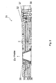
- FIG. 2 shows in section a gas shower electrode assembly according to the invention with three gas distribution plates, which are fitted in a holder 39 made of stainless steel. It is on average a first gas distribution plate 32, which is aligned with the substrate (not shown in the figure, but to be placed above the electrode 31). This is attached with two screws 37 to the bracket. A second gas distribution plate 33 and a third gas distribution plate 34 are separated by spacer rings 38. The diameter of the gas distribution plates increases continuously from the gas distributor plate 32 to the gas distributor plate 34.
- the hole in plate 32 has an inner diameter of 10 mm, in plate 33 16 mm and in plate 34 19 mm.
- Reference numeral 35 designates a stepped funnel as a physically existing component.
- the funnel 35 has marginal, outwardly directed steps on which the gas distribution plates 32, 33 and 34 are placed.
- a Matterschante is arranged, which carries in its edge two or more holes. The holes are provided for the screws 36. Only the left of the two screws 36 is provided with reference numerals.
- the entire electrode 31 of the plates and the holder 39 is by means of ceramic holders 52, as in FIG. 4 shown attached in the plasma chamber.
- the gas distribution plates 32 to 34 allow a homogeneous gas distribution in the plasma chamber (above in the figure). By an increasing number of gas distribution holes per gas distribution plate from bottom to top in the figure, the necessary pressure drop is achieved. As a result, the gas flows homogeneously from the uppermost plate 32 into the plasma chamber above. For this purpose, the gas is first introduced into the region arranged below plate 34.
- the funnel in the optical feedthrough prevents gas leakage through the optical feedthrough and keeps it gas-tight.
- the angle of the cone and the size of the passage 35 through the pitch pattern of the gas distribution plates is predetermined by the three gas distribution plates themselves. This should be changed as little as possible by the implementation 35.
- the diameter of the upper opening of the passage in the cone is 1 cm, the diameter of the lower opening is 2.2 cm.
- the conical feedthrough was chosen in order to achieve the greatest possible acceptance angle for the collection of the electromagnetic radiation with a small opening in the upper electrode.
- the gas shower electrode has a diameter of 13.7 cm.
- substrate sizes of up to 5.7 m 2 are meanwhile being coated industrially.
- the substrate need not be disposed above the electrode 32.
- the showerhead electrode can also be above the substrate. This corresponds to an "upside down" arrangement in FIG. 2 , Also electrode and counter electrode can be arranged vertically. This corresponds to a tilt of 90 °.
- FIG. 3 schematically shows the arrangement in a vacuum chamber 41 according to the invention.
- the arrangement of the turbo pump 47 in this example a linear beam guidance is not possible, therefore, the 45 ° deflection by the mirror 46 is necessary.
- the distance from the RF electrode 44 according to the invention and thus the distance of the lens 45 to the substrate 43 is adjustable in height and adjustable from about 5 mm to about 25 mm. This corresponds to the intervals used in industry for the deposition of silicon during the PECVD process.
- Reference numeral 42 denotes the counter electrode on which the substrate 43 is arranged.
- An unillustrated excitation laser generates the radiation 48, which is focused through a window 50 in the chamber wall and via the condenser lens 45 onto the substrate or a layer deposited thereon.
- Reference numeral 49 shows the (Raman) radiation collected by the lens which is guided by the lens 45 onto the mirror 46. From the mirror 46, the radiation 49 is supplied to the spectrometer (not shown) for further analysis. The angle of incidence is zero degrees.
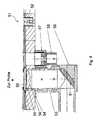
- FIG. 4 indicates the practical implementation FIG. 3 in technical section.
- the plano-convex focusing lens 56 serves to focus the excitation radiation on the sample and to collect the Raman radiation (not shown).
- the focal length of the lens 56 is chosen so that the substrate surface is in focus (here 38 mm).
- the lens 56 is clamped with a screw 55 in the holder.
- the glass plate 60 over the lens 56 was installed to prevent the coating of the lens during the deposition of the sample layer (not shown). It allows advantageous easy cleaning of the optics.
- the optical implementation is not shown in this figure.
- a mirror 61 is arranged at 45 ° to the bracket.
- the mirror 61 is arranged together with the lens 56 in a holder.
- This holder 53 is height-adjustable attached to the electrode to different spectroscopic distances between electrode and layer and the layer itself can. The height adjustment is ensured by a screw in a slot (not visible in this drawing).
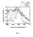
- FIG. 5 shows the in-situ measurement of the intensity of the Stokes shift as a function of the magnitude of the shift as a basis of a Raman spectroscopy, which was carried out by means of the assembly according to the invention with optical implementation and arrangement in the plasma chamber. Shown are measurements in different stages of the layer deposition. After about 12 nm deposited silicon layer, a signal can be seen, which can be assigned to the glass surface. After approx. 240 nm, the measuring signal shows a typical characteristic of microcrystalline silicon.
- the Stokes shift of microcrystalline silicon can be split into two parts. The first part is caused by the microcrystalline phase and has its intensity maximum at ⁇ 520 cm -1 . Of the second part is caused by the amorphous phase.
- Its intensity maximum is ⁇ 480 cm -1 . Since the deposition occurs at about 200 ° C, the intensity maximum of the microcrystalline phase is at a Stokes shift of about 505 relative wavenumbers, that of the amorphous at ⁇ 460 cm -1 . With a thickness of the deposited layer of about 720 nm, the signal is even more pronounced, because the contribution of the glass substrate is now completely suppressed.
- FIG. 6a shows the in-situ measurement of the intensity of the optical emission of the plasma as a function of the wavelength in a range of 505 nm to 570 nm by the inventive construction of electrode with optical implementation and arrangement in the plasma chamber. Measured in a larger spectral range , as in FIG. 6b ), you can z. B. use the ratio of two emission lines to determine gas concentrations in the plasma.
Landscapes
- Chemical & Material Sciences (AREA)
- Engineering & Computer Science (AREA)
- Physics & Mathematics (AREA)
- Chemical Kinetics & Catalysis (AREA)
- Materials Engineering (AREA)
- Mechanical Engineering (AREA)
- Metallurgy (AREA)
- Organic Chemistry (AREA)
- Plasma & Fusion (AREA)
- General Chemical & Material Sciences (AREA)
- Spectroscopy & Molecular Physics (AREA)
- Analytical Chemistry (AREA)
- General Physics & Mathematics (AREA)
- Investigating, Analyzing Materials By Fluorescence Or Luminescence (AREA)
- Chemical Vapour Deposition (AREA)
Description
- Die Erfindung betrifft eine Elektrode zur Erzeugung eines Plasmas, eine Plasmakammer mit dieser Elektrode und ein Verfahren zur in situ-Analyse oder -in situ-Bearbeitung einer Schicht oder des Plasmas.
- Aus Li et al. (Li, Y.M., Ilsin A.N., Ngyuen H.V., Wronski C.R., Collins R.W. (1991). Real-Time-Spectroscopic Ellipsometry Determination of the Evolution of Amorphous-Semiconductor Optical Functions, Bandgap, and Micrsotructure. Journal of Non-Crystalline Solids. Vol. 137,787-790) ist die in situ Charakterisierung einer amorphen Schicht während der plasmaunterstützten chemischen Gasphasenabscheidung (engl. plasma enhanced chemical vapour deposition (PECVD) bekannt. Als Verfahren verwenden die Autoren eine Spektroskopische Ellipsometrie unter Einstrahlung von Licht im 70° Winkel. Nachteilig ist mit dem Verfahren und dem angewendeten Ellipsometer nur eine vergleichsweise begrenzte Aussage über die Schichteigenschaften möglich.
- Wagner et al. (Wagner V., Drews, D., Esser, D.R., Zahn, T., Geurts, J., and W. Richter. Raman monitoring of semiconductor growth. J. Appl. Phys. 75, 7330) beschreiben eine in situ Raman Spektroskopie an einer mit Molekularstrahlepitaxie abgeschiedenen Schicht. Das Verfahren und der Aufbau der verwendeten Vorrichtung weisen den Nachteil auf, dass diese nicht uneingeschränkt von der Art des verwendeten Abscheidungsverfahrens angewendet werden können.
- Aus Dingemans et al. (Dingemans, G.; van den Donker, M. N.; Hrunski, D.; Gordijn, A.; Kessels, W. M. M.; van de Sanden, M. C. M. (2007). In-Situ Film Transmittance Using the Plasma as Light Source: A Case Study of Thin Silicon Film Deposition in the Microcrystalline Growth Regime. Proceedings of the 22nd EUPVSEC (European Photovoltaic Solar Energy Conference), Milan/Italy, 03.09.2007 - 07.09.2007. - S. 1855 -1858) ist bekannt, eine optische Emissions-Spektroskopie am Plasma einer Plasmakammer in situ durchzuführen. Hierzu ist in der Gegenelektrode der Plasmakammer eine optische Durchführung vorhanden, mit der das Plasma direkt durch das Substrat hindurch untersucht werden kann. Nachteilig ist auch diese Vorrichtung nicht geeignet, weitergehende Informationen zum Verfahren zu sammeln.
- Aus der
US 2006/196846 A1 ist eine rf-Elektrode zur Erzeugung eines Plasmas in einer Plasmakammer bekannt, die mit mindestens einer optischen Durchführung ausgestattet ist, wobei die rf-Elektrode eine Gasdusche ist.
Aus derUS 2005/029228 A1 ist ein optisches Detektionssystem bekannt, das in eine Elektrode integriert ist und eine zylindrische Durchführung aufweist.
Aus derWO 2007/022144 A1 ist eine Vorrichtung zur Verbesserung der optischen Abtastung von einem Plasmaprozess durch die Verwendung eines faseroptischen Sensors in einer Gasdusche bekannt. Das Licht wird durch eine Öffnung in der Gasdusche detektiert. Ein spezieller Schutz oder eine spezielle Ausgestaltung der Öffnung zum Schutz der optischen Elemente wird nicht offenbart.
Aus derUS 2004/0118518 ist ein optisches Detektionssystem bekannt, welches ebenfalls in eine Gasdusche integriert ist. Um lokale unerwünschte Entladungen in der Öffnung zur optischen Messung zu vermeiden, sind im Bereich der optischen Durchführung eine Mehrzahl kleiner Löcher vorhanden. - Aufgabe der Erfindung ist es, eine Elektrode zur Erzeugung eines Plasmas in einer Plasmakammer bereit zu stellen, die sowohl unabhängig vom verwendeten Abscheidungsverfahren, wie z. B. PECVD, MOVPE, als auch unabhängig von der gewählten Untersuchungsmethode, wie z. B. die Raman Spektroskopie und die optische Emissionsspektroskopie, universell eingesetzt werden kann.
- Eine weitere Aufgabe der Erfindung ist es, eine Plasmakammer bereit zu stellen, mit der unabhängig vom Herstellungsverfahren der Schicht eine Vielzahl an Untersuchungsmethoden in situ ermöglicht wird.
- Eine weitere Aufgabe der Erfindung ist es, ein Verfahren anzugeben, mit dem die Analyse einer abzuscheidenden Schicht, als auch der Prozessgase während des laufenden Herstellungsverfahrens, in situ durchgeführt werden kann.
- Die Aufgabe wird gelöst durch eine rf-Elektrode nach dem Hauptanspruch, eine Plasmakammer mit einer derartigen Elektrode und durch ein Verfahren nach den Nebenansprüchen. Vorteilhafte Ausgestaltungen ergeben sich aus den jeweiligen Unteransprüchen.
- Es handelt sich erfindungsgemäß um eine rf-Elektrode für die Erzeugung des Plasmas mittels einer Hochfrequenzspannung. Das Plasma kann z. B. für die Abscheidung von Halbleiter-Schichten oder zur Plasmaätzung von Halbleiter-Schichten genutzt werden. Im ersten Falle werden Gase wie SiH4 oder H2, und im zweiten Fall ein Gas wie NF3 in die Kammer geleitet.
- Die rf-Elektrode ist erfindungsgemäß dadurch gekennzeichnet, dass sieb eine optische Durchführung umfasst. Die optische Durchführung gewährt vorteilhaft einen optischen Zugang sowohl auf den Plasmaraum selbst, als auch durch den Plasmaraum hindurch bis zum Substrat, welches auf der Gegenelektrode (auch Masseelektrode genannt) angeordnet ist. Der Durchtritt eines Strahlengangs durch die optische Durchführung der erfindungsgemäßen rf-Elektrode ist damit gewährt. Dadurch wird vorteilhaft bewirkt, dass sowohl die Analyse als auch die Bearbeitung des Substrats und der hierauf aufwachsenden Schicht während das Plasma brennt ermöglicht wird. Besonders vorteilhaft wird durch die Anordnung der optischen Durchführung in der rf-Elektrode bewirkt, dass in der Plasmakammer auch das Plasma selbst auf die Gaszusammensetzung hin untersucht und diese nachjustiert werden kann.
- Dadurch wird eine weitgehende Freiheit bei der Wahl der Untersuchungsmethode und Bearbeitungsmethode erreicht.
- Im Rahmen der Erfindung wurde erkannt, dass der Stand der Technik, sowohl in Hinblick auf die Anordnung einer optischen Durchführung in der Gegenelektrode bei Dingemans et al., als auch mit Blick auf die angewendeten Untersuchungsverfahren in Li et al. sowie der Abscheidungsverfahren in Wagner et al., limitiert sind. Nur die erfindungsgemäße rf-Elektrode gewährleistet, dass bei mehr oder weniger jedem Abscheidungsverfahren (PECVD, MOVPE und andere) in situ verschiedenste Untersuchungs- oder Bearbeitungsschritte der Schicht sowie auch des Plasmas ermöglicht werden. Das erfindungsgemäße Verfahren nutzt durch den Rückgriff auf die erfindungsgemäße rf-Elektrode sowohl für den Eintritt in den Plasmaraum, als auch für den Austritt elektromagnetischer Strahlung, einen Einfallswinkel von etwa Null Grad zur abzuscheidenden Schicht. Dadurch wird vorteilhaft bewirkt, dass auch Raman Spektroskopie an einer wachsenden Schicht oder lokal aufgelöste, optische Emissionsspektroskopie am Plasma während das Plasma brennt (in situ) durchgeführt werden kann. Die Bearbeitung der Schicht kann einen Bearbeitungsschritt mit einem Laser umfassen.
- Besonders vorteilhaft wird durch die optische Durchführung in der rf-Elektrode bewirkt, dass eine direkte Beobachtung einer Schicht durch Ein- und Auskopplung des Lichts mit einem Einfallswinkel von etwa Null Grad zur Schicht ermöglicht wird. Geringfügige Abweichungen vom Null Grad Einfallswinkel sind denkbar.
- Im Stand der Technik wird hingegen im 70° Winkel zur Schicht der Strahlengang zur Analyse der Schicht eingestrahlt. Dies hat den Nachteil, dass ein großer Teil des Abscheidungsraumes in der Plasmakammer mitbetrachtet und fälschlich auch analysiert und interpretiert wird. Im Rahmen der Erfindung wurde erkannt, dass diese Form der in situ-Analyse fehlerbehaftete Ergebnisse bei der Interpretation der Schichteigenschaft oder der Plasmaeigenschaft lieferte.
- Es wurde zudem erkannt, dass bisher, vor allem bei kleinen Elektrodenabständen relativ zur Elektrodenfläche, nur die Analyse eines Randbereichs der Schicht oder aber nur unter einem bestimmten Winkel auch der produktionsrelevante Teil analysiert werden konnte. Viele Untersuchungen, wie die Raman Spektroskopie, können im Stand der Technik wie in Dingemans et al., aber erst nach der Abscheidung durchgeführt werden. Mit Randbereich der Schicht wird der Teil der wachsenden Schicht bezeichnet, der außerhalb des optimalen Nutzungsbereichs der Elektrode liegt, bzw. der für die spätere Anwendung der Schicht irrelevant ist. Dadurch sind bestimmte Messmethoden, wie z. B. die Raman Spektroskopie oder die Reflexionsspektroskopie, als besonders einträgliche Verfahren zur Charakterisierung einer abgeschiedenen Schicht in Echtzeit, das heißt noch während der Abscheidung, ausgeschlossen. Der Begriff in situ der vorliegenden Patentanmeldung meint also die Analyse oder Bearbeitung des Substrats oder einer hierauf angeordneten oder abzuscheidenden Schicht während das Plasma brennt, das heißt in Echtzeit.
- Im Gegensatz zu dem Stand der Technik können mit der erfindungsgemäßen rf-Elektrode auch produktionsrelevante Bereiche der Schicht in Echtzeit analysiert und bearbeitet werden, und nicht nur die Randbereiche.
- Als Analyse gilt insbesondere die in situ Raman Spektroskopie. Durch Einkoppeln eines gepulsten Laserstrahls durch die optische Durchführung der rf-Elektrode hindurch auf die Schicht und durch Spektroskopie des gestreuten Lichts in der direkten Rückreflexion kann während einer Abscheidung, z. B. von Material für eine Dünnschichtsolarzelle, eine Raman Spektroskopie durchgeführt werden. Dadurch ist es möglich, das Wachstum und die strukturellen Eigenschaften der Schicht während der Abscheidung besser zu überwachen.
- Als Analyse gilt auch die ortsaufgelöste Emissionsspektroskopie. Mit Hilfe eines konfokalen Aufbaus mit einer fixiert angeordneten oder verschiebbaren Linse im Strahlengang, können die Plasma Emissionen über einer wachsenden Siliziumoberfläche ortsaufgelöst, das heißt in unterschiedlichen Abständen von der Oberfläche der Schicht, spektroskopiert werden. Die Linse kann fixiert an der rf-Elektrode angeordnet werden. Die Linse kann aber auch im Gehäuse der Plasmakammer fixiert werden. Die Linse kann aber auch im Gehäuse verschiebbar angeordnet werden, so dass ein für unterschiedliche Anwendungen konfokaler Messplatz erreicht wird. Es sind andere Verfahren wie die Reflexionsspektroskopie anwendbar. Es kann zudem zum selben Zweck die rf-Elektrode mit hieran fixierter Linse im Strahlengang des Messplatzes verschiebbar zur untersuchenden Schicht angeordnet werden.
- Die optische Durchführung verläuft durch die rf-Elektrode hindurch von einer Seite der Oberfläche auf die dieser Seite gegenüberliegende Seite der rf-Elektrode. Mit Durchführung ist im Sinne der Erfindung also eine Öffnung durch die Konstruktion der Elektrode umfasst, die den Durchtritt von elektromagnetischer Strahlung, insbesondere Laserstrahlung zur Abtastung in Richtung der wachsenden Schicht, gewährleistet. Die optische Durchführung gewährleistet andererseits den Durchtritt der von der Schicht oder dem Plasma ausgehenden Strahlung (z. B. Reflektion, Streuung oder Wärmestrahlung) zurück auf ein Analysegerät. Auch Temperaturmessungen der Schicht sind gewährleistet. Die Elektrode mit der optischen Durchführung ist demnach im Strahlengang der in die Plasmakammer eingekoppelten Strahlung angeordnet.
- Die Elektrode ist besonders vorteilhaft in eine Plasmakammer integriert, in der ein Vakuum erzeugt werden kann. Die Elektrode ist von der Kammerwand elektrisch isoliert. Die rf-Elektrode ist mit einer Anschlussmöglichkeit für eine Hochfrequenz Wechselspannung (rf-Anschluss: 30 kHz-300 GHz Oszillation, vorzugsweise 13,56 MHz bis 108,48 MHz) versehen. Die Wechselspannung eines rf-Generators wird an die Metallplatte als Elektrode angelegt, die sich in einer Niederdruckkammer befindet. Parallel zur rf-Elektrode und dieser gegenüberliegend ist die Gegenelektrode mit dem Substrathalter angeordnet.
- Die Vakuumkammer enthält vorteilhaft ein Fenster als eine optische Durchführung in ihrer Wand, durch das die elektromagnetische Strahlung ein- und wieder ausgekoppelt werden kann.
- Die aus der Plasmakammer ausgekoppelte Strahlung wird vorteilhaft durch das Linsen- und gegebenenfalls auch Spiegelsystem geführt und auf den Eintrittsspalt eines Spektrographen, wie z. B. eines Oriel Instruments MS260, fokussiert. Mithilfe des Spektrographen wird die Strahlung in ihre spektroskopischen Bestandteile zerlegt, die mittels einer CCD Kamera, z. B. einer Andor iDus 420, analysiert werden. Im Falle einer Raman Spektroskopie ist in den optischen Weg von der Substratoberfläche zum Spektroskop ein optischer Kerbfilter angeordnet. Der Kerbfilter bewirkt vorteilhaft, dass die zur Anregung der Raman Streuung genutzte Wellenlänge mit sehr schmaler Bandbreite unterdrückt wird.
- Der optische Zugang zur Schicht bzw. zum Plasma über der Schicht ist im einfachsten Fall ein Loch, vorzugsweise in der Mitte oder in der Nähe der Mitte der rf-Elektrode, so dass produktionsrelevante Teile des Substrats, bzw. der abzuscheidenden Schicht, analysiert oder bearbeitet werden können. Auch dies ist mit Elektroden nach dem Stand der Technik nicht möglich.
- Die rf-Elektrode weist besonders vorteilhaft eine optische Durchführung auf, welche zur Plasmakammer gerichtet geschirmt ist. Die Schirmung erfolgt vorzugsweise mit einem metallischen Gitter, welches auf der Öffnung der optischen Durchführung angeordnet ist. Dadurch wird vorteilhaft bewirkt, dass das von der Elektrode erzeugte elektrische Feld nicht gestört wird.
- Im Rahmen der Erfindung wurde erkannt, dass die optische Durchführung abhängig von den Parametern des verwendeten Abscheidungsverfahren zu Inhomogenitäten in der Schichtabscheidung oder während einer Ätzung aufgrund eines gestörten elektrischen Feldes führten kann. Deshalb wurde die optische Durchführung der rf-Elektrode zum Plasmaraum hin, vorzugsweise durch ein Metallgitter, so geschirmt, dass ein optischer Zugang mit kleinen Verlusten möglich ist. Dadurch wird vorteilhaft bewirkt, dass das von den Elektrodenplatten erzeugte Hochfrequenzfeld weitestgehend unbeeinflusst durch die optische Durchführung ist.
- Dies gilt insbesondere für den besonders vorteilhaften Fall, dass die optische Durchführung Bestandteil einer Gasduschenelektrode als rf-Elektrode (engl. Showerhead-Elektrode) ist.
- In diesem Fall ist die optische Durchführung in der Gasduschenelektrode als rf-Elektrode integriert, so dass die Homogenität der Gasverteilung nicht gestört ist. Dies gelingt durch die Wahl eines Standorts für die optische Durchführung, bei dem nur wenige oder bestenfalls gar keine Löcher für den Gasdurchtritt durch die optische Durchführung beeinflusst werden.
- Die optische Durchführung und das metallische Gitter als Schirmung können aus demselben Material bestehen, z. B. aus VA-Stahl oder Aluminium.
- Das Gitter als Schirmung kann vorzugsweise durch Laserstrahlschneiden hergestellt werden. Die Dicke der Gitterstege kann etwa 0,3 mm betragen und die Stegbreite z. B. etwa 0,1 mm. Die Öffnung der optischen Durchführung kann vorzugsweise zu 12 bis 19 % durch die Stege der Schirmung bedeckt sein. Eine Bedeckung der Öffnung durch die Schirmung zu etwa 10 % sollte genug sein, um die Homogenität des Plasmas zu erhalten. Eine optimale Schirmung bekäme man auch durch eine Metallplatte, durch die aber selbstverständlich keine Analysen oder Bearbeitungsschritte des Substrats oder des Plasmas möglich sind. Auch mit weniger als 10 % an bedeckter Oberfläche der Öffnung der optischen Durchführung ist eine Schirmung grundsätzlich möglich. Die genaue prozentuale Bedeckung der Öffnung der optischen Durchführung durch die Schirmung hängt von den Prozessbedingungen, z. B. vom eingesetzten Druck in der Plasmakammer, ab. Bei einem Druck von >18 Torr, einem Elektrodenabstand von 9 mm, einer Leistungsdichte von ∼1 W/cm2 und einer Wachstumsrate von 0,5 nm/s ist bei der Abscheidung von mikrokristallinem Silizium, bei einem dem Substrat zugewandten Lochdurchmesser von 1 cm, gar keine Schirmung der optischen Durchführung nötig.
- Bei einem Druck von 10 Torr, einem Elektrodenabstand von 9 mm, einer Leistungsdichte von 0,6 W/cm2 und einer Wachstumsrate von 0,5 nm/s sollte bei der Abscheidung von mikrokristallinem Silizium, bei einem dem Substrat zugewandten Lochdurchmesser von 1 cm, etwa 10 % der Öffnung der optischen Durchführung durch die Schirmung bedeckt sein.
- In der erfindungsgemäßen Plasmakammer ist im Falle einer Schirmung die zur Abscheidungszone gerichtete Öffnung der optischen Durchführung geschirmt. Als Plasmakammer bezeichnet man üblicherweise die ganze Vakuumkammer.
- Die optische Durchführung muss allgemein so groß sein, dass durch die erfindungsgemäße Elektrode hindurch das angestrebte Untersuchungsverfahren ermöglicht wird. Dies kann z. B. eine in situ Raman Spektroskopie oder eine optische Emissionsspektroskopie, oder z. B. die Bestimmung der Gaskonzentrationen auf optischem Weg sein. Die Fläche der optischen Durchführung sollte etwa mindestens 0,03cm2 betragen. Bei kreisrunden optischen Durchführungen entspricht dies einem Durchmesser der zur Abscheidungszone gerichteten Öffnung von mehr als 2 mm. Vorzugsweise weist die Öffnung eine Fläche von 1 bis 10 cm2 auf.
- Eine Linse kann an der rf-Elektrode oder allgemein in der Plasmakammer angeordnet sein. Die Linse soll für ein erfindungsgemäßes Verfahren die elektromagnetische Strahlung durch die optische Durchführung hindurch auf das Plasma oder die Schicht bzw. das Substrat fokussieren. Dieselbe Linse oder, je nach Einfallswinkel der Strahlung, eine Linse einer weiteren optischen Durchführung in der rf-Elektrode parallelisiert die von dem Substrat oder vom Plasma durch die optische Durchführung hindurch reflektierte oder gestreute oder emittierte elektromagnetische Strahlung.
- Vorzugsweise beträgt der Einfallswinkel der elektromagnetischen Strahlung auf das Substrat bzw. die Schicht Null Grad. Eine geringe Abweichung hiervon ist möglich, so dass für den Zugang zum produktionsrelevanten Teil der Schicht bzw. der Entladungszone ein kleinerer Einfallswinkel möglich ist, als bei einem Zugang durch den Raum seitlich zwischen den Elektroden.
- Die Größe der optischen Durchführung ist also keineswegs mit der Größe der Öffnungen der Löcher in einer Gasduschenelektrode nach dem Stand der Technik zu verwechseln und daher auch nicht hiermit zu vergleichen. Diese haben üblicherweise einen Durchmesser von nur etwa 0,8 mm entsprechend etwa 0,005 cm2 Fläche. Diese Öffnungen nach dem Stand der Technik sind ungeeignet für eine erfindungsgemäße Analyse oder Bearbeitung der Schicht oder des Plasmas auf optischen Weg.
- Die optische Durchführung führt vollständig durch die Elektrode hindurch. Somit weist die Elektrode eine erste Öffnung auf der einen Seite der Oberfläche und eine zweite Öffnung auf der dieser Oberfläche gegenüberliegenden Oberfläche der Elektrode auf. Beide Öffnungen der optischen Durchführung können den gleichen Durchmesser aufweisen. Dann ist die erfindungsgemäße Elektrode besonders leicht herstellbar.
- Die optische Durchführung weist einen konischen Schnitt auf. Die optische Durchführung ist konisch in der Elektrode angeordnet. In der konischen Durchführung weist die zum Plasmaraum gerichtete Öffnung eine größere Fläche auf, als die dieser Öffnung gegenüberliegende Öffnung der optischen Durchführung. Vorteilhaft wird dann bewirkt, dass elektromagnetische Strahlung von der Schicht oder dem Plasma ausgehend effizienter gesammelt und dem Analysegerät zugeführt werden kann.
- Es wurde erkannt, dass im einfachsten Falle die optische Durchführung durch ein einzelnes z. B. zylinderförmiges Loch in der Elektrode realisiert werden kann. Es kann z. B. mit einem 10 mm Bohrer die rf-Elektrode durchbohrt werden. Es ist aber auch möglich, stattdessen mit einem Senker eine konische Durchführung in die rf-Elektrode einzubringen.
- Die kleinere der beiden Öffnungen einer konischen optischen Durchführung kann eine Fläche von 0,03 cm2 bis 5 cm2 aufweisen. Die größere der beiden Öffnungen der konischen optischen Durchführung kann eine Fläche von 0,031 bis 100 cm2 aufweisen. Besonders vorteilhaft ist die Fläche der größeren Öffnung der optischen Durchführung bis 20 mal größer.
- Allgemein hängt die Größe der Öffnung, welche vom Substrat abgewandt ist bei gegebenem Winkel des Konus von der Dicke der erfindungsgemäßen Elektrode ab.
- Vorzugsweise strömt durch die optische Durchführung kein Gas oder genauso viel Gas wie aus einer gleich großen Fläche einer unmodifizierten Gasduschenelektrode in den Plasmaraum. Dadurch wird vorteilhaft bewirkt, dass die Homogenität des Gasflusses durch die optische Durchführung nicht gestört wird.
- Eine optische Durchführung kann zusätzlich zu einem einfachen Loch in der Elektrode durch ein Bauteil ausgebildet werden. Diese kleidet das Loch in der Elektrode hülsenartig aus. In einer Gasduschenanordnung als rf-Elektrode sind beispielweise drei Gasverteilerplatten unterschiedlichen Durchmessers übereinander angeordnet, wie z. B. in
Figur 2 gezeigt. Diese bilden die erfindungsgemäße Gasdusche als rf-Elektrode aus. In den drei Gasverteilerplatten ist jeweils ein Loch unterschiedlicher Größe zur Ausbildung der optischen Durchführung angeordnet. In der Elektrode sind diese übereinander angeordnet, so dass eine konische optische Durchführung gebildet wird. In der Gasdusche ist zusätzlich ein trichterförmiges konisches Bauteil für die Ausbildung der konischen optischen Durchführung angeordnet. Dieses Bauteil kleidet die optische Durchführung von innen aus. Der Trichter weist hierzu stufenförmige Auflageflächen für die Gasverteilerplatten auf. Haltemittel, wie Schrauben, befestigen die Platte(n) an dem Trichter. Durch die Wand des trichterförmigen Bauteils wird vorteilhaft ein Einströmen des Gases in den Plasmaraum durch die optische Zuführung verhindert. Der Trichter sorgt hier für Gasdichtigkeit der optischen Durchführung. - Auch hier kann, abhängig von den Parametern des Abscheidungsverfahrens, ein Metallgitter als Schirmung auf der kleineren Öffnung des trichterförmigen Bauteils angeordnet sein.
- In einer weiteren Ausgestaltung der Erfindung ist an der optischen Durchführung der rf-Elektrode eine konvexe, insbesondere eine plankonvexe Sammellinse fixiert angeordnet. Diese bewirkt vorteilhaft, dass zu Analysezwecken oder zu Bearbeitungszwecken elektromagnetische Strahlengang durch die optische Durchführung hindurch auf das Substrat bzw. die aufwachsende Schicht oder in das Plasma geleitet und auf dessen Oberfläche fokussiert wird. Hierdurch ist es möglich, durch den hohen Energieeintrag eines gepulsten Lasers eine Raman Emission des Substrats bzw. der Schicht hervorzurufen und somit eine Raman Spektroskopie an der zurückgeworfenen Strahlung durchzuführen. Außerdem kann das Licht oder allgemein die elektromagnetische Strahlung mithilfe der Linse gesammelt und fokussiert und auch parallelisiert werden.
- Die Linse ist dann auf der nicht zum Plasmaraum ausgerichteten Seite der optischen Durchführung angeordnet. Im Falle einer zusätzlich vorhandenen Schirmung ist die Linse entsprechend auf einer Seite der Öffnung, welche der Schirmung gegenüberliegt, angeordnet.
- Besonders bevorzugt ist zwischen der Sammellinse und der Öffnung der optischen Durchführung ein austauschbares Glasplättchen zum Schutz der Sammellinse angeordnet. Dadurch wird vorteilhaft bewirkt, dass die Linse nicht beschichtet wird während das Plasma brennt. Dadurch wird vorteilhaft bewirkt, dass bei einer Reinigung der Kammer die Linse nicht ausgebaut werden muss. Somit muss die Optik vorteilhaft nach der Reinigung nicht neu justiert werden.
- Eine erfindungsgemäße Plasmakammer umfasst die rf-Elektrode mit einer oder mehreren optischer Durchführungen und einem rf-Hochfrequenzanschluss.
- In der Kammer ist eine geerdete oder schwebende Gegenelektrode mit einem darauf angeordneten Substrat angeordnet. Zwischen der Elektrode und der Gegenelektrode wird ein Hochfrequenzwechselfeld zur Erzeugung des Plasmas ausgebildet. Die Kammer weist erfindungsgemäß die rf-Elektrode mit der optischen Durchführung auf. Dadurch wird vorteilhaft bewirkt, dass elektromagnetische Strahlung durch die optische Durchführung auf das Substrat bzw. die darauf wachsende Schicht oder in das Plasma selbst gerichtet werden kann. Dadurch kann das Substrat, die Schicht oder die Gaszusammensetzung in der Kammer während der Abscheidung und während das Plasma brennt, in situ untersucht werden.
- Die zum Innem der Plasmakammer ausgerichtete Öffnung der optischen Durchführung ist vorteilhaft geschirmt, so dass eine besonders homogene Abscheidung oder Ätzung der auf dem Substrat angeordneten Schicht erzeugt wird.
- Eine konvexe Sammellinse auf der der Plasmakammer abgewandten Seite der optischen Durchführung fokussiert den Strahlengang auf das Substrat bzw. auf die auf dem Substrat aufwachsende Schicht oder auf das Plasma selbst. Die Linse sammelt, fokussiert und parallelisiert die reflektierte oder gestreute oder von der Probenoberfläche ausgehende Strahlung der Schicht zum Zwecke der Analyse. Das heißt, die von der Schicht reflektierte oder gestreute oder emittierte Strahlung wird wiederum durch die optische Durchführung auf dem Rückweg gesammelt und aus der Plasmakammer herausgeleitet.
- Die erfindungsgemäße rf-Elektrode und die erfindungsgemäße Kammer ermöglichen im Sinne einer einheitlichen Idee somit ein Verfahren zur in situ-Analyse oder in situ-Bearbeitung einer Schicht in der Plasmakammer sowie auch des Plasmas, während dieses brennt. Das Substrat ist auf der Gegenelektrode angeordnet.
- Auf der dem Substrat zugewandten Seite wird in einem Abstand X zum Substrat die rf-Elektrode angeordnet. Die zur Abscheidung oder Ätzung verwendeten Prozessgase werden eingelassen und der Prozessdruck eingestellt. Sodann wird das Plasma gestartet.
- Für das Verfahren wird in einer Ausgestaltung der Erfindung eine Elektrode mit einer optischen Durchführung gewählt, welche auf der dem Substrat zugewandten Seite der Elektrode eine Schirmung aufweist. Besonders vorteilhaft wird auf der der Schirmung gegenüber liegenden Seite der Elektrode eine plankonvexe Sammellinse angeordnet.
- Vorzugsweise wird eine Sammellinse gewählt, die eine Brennweite X plus die Dicke der Elektrode aufweist. Dadurch wird vorteilhaft bewirkt, dass ein durch die optische Durchführung hindurch tretender Strahlengang auf das Substrat fokussiert wird. Reflektierte oder gestreute oder von der Schichtoberfläche emittierte Strahlung wird durch die Linse hingegen gesammelt und parallelisiert aus der Kammer geleitet. Zu diesem Zweck kann die reflektierte oder gestreute oder von der Schichtoberfläche emittierte Strahlung zunächst je nach Aufbau der Analysevorrichtung und Platzangebot auf einen Spiegel geleitet werden.
- Besonders bevorzugt ist die Plasmakammer mit einer Verstellbarkeit der Sammellinse entlang des Strahlengangs. Hierzu wird die Linse im Gehäuse der Plasmakammer verschiebbar befestigt. Eine Plasmakammer mit einem Halter wird gewählt, welcher höhenverstellbar an der Elektrode befestigt ist. Die Linse kann auch an der rf-Elektrode fixiert sein und die Elektrode selbst ist verschiebbar. Mit beiden Aufbauten wird vorteilhaft bewirkt, dass verschiedene Bereiche zwischen der rf-Elektrode und der Schicht sowie die Schicht als auch das Plasma selbst variabel spektroskopiert werden können. Die Höhenverstellbarkeit kann durch eine Schraube in einem Langloch gewährleistet werden.
- Dadurch kann das System während des Verfahrens an verschiedene Linsen- und Elektrodenabstände angepasst werden. Außerdem wird auf diese Weise die Untersuchung der aufwachsenden Schicht als auch des Plasmas ermöglicht. Selbstverständlich kann für das Verfahren aber auch die Sammellinse an der Elektrode selbst befestigt werden.
- Vorzugsweise wird eine in situ-Raman Spektroskopie durch Sammeln von Phononen mittels der Sammellinse durchgeführt, wobei die Linse das zum Substrat gerichtete Licht auf die zu untersuchende Schicht fokussiert, und die von der Schicht reflektierte oder gestreute oder von der Schichtoberfläche emittierte Strahlung parallelisiert aus der Kammer leitet.
- Mit dem Begriff Schicht ist erfindungsgemäß auch das Substrat selbst gemeint.
- Im Weiteren wird die Erfindung anhand von Ausführungsbeispielen und der Figuren näher beschrieben, ohne dass hierdurch eine Einschränkung der Erfindung stattfindet.
- Es zeigen:
- Figur 1:
- Schnitt durch die erfindungsgemäße rf-Elektrode und Plasmakammer (Schemazeichnung).
- Figur 2:
- Schnitt durch die erfindungsgemäße Gasduscheelektrode (technische Zeichnung).
- Figur 3:
- Schnitt durch die erfindungsgemäße Plasmakammer (Schemazeichnung).
- Figur 4:
- Schnitt durch die erfindungsgemäße Plasmakammer (technische Zeichnung).
- Figur 5:
- Durch den erfindungsgemäßen Aufbau aus rf-Elektrode mit optischer Durchführung und Anordnung in der Plasmakammer erfolgte in situ-Messung der Intensität der Stokes-Verschiebung in Abhängigkeit von der Größe der Verschiebung als Basis einer Raman Spektroskopie.
- Figur 6:
- Durch den erfindungsgemäßen Aufbau aus Elektrode mit optischer Durchführung und Anordnung in der Plasmakammer erfolgte in situ Messung der Wellenlänge in Abhängigkeit von der Intensität als Basis für die Bestimmung der SiH4-Konzentration in der Plasmakammer.
-
Figur 1 zeigt das Prinzip der Lösung der Aufgabe der Erfindung durch eine optische Durchführung. An der Elektrode 1, der Gegenelektrode, ist das Substrat 6 angeordnet. Die erfindungsgemäße rf-Elektrode 2 weist die optische Durchführung auf, die groß genug ist eine Analyse oder Bearbeitung des Substrats oder des Plasmas in situ vorzunehmen. Der Strahlengang wird hierzu im Null Grad Einfallswinkel zum Substrat auf dieses geleitet und durch die Linse fokussiert. Der Bereich der optischen Durchführung ist mit Bezugszeichen 5 angegeben. Der Konus der Durchführung 5 mit der kleineren Öffnung zum Substrat gerichtet bewirkt vorteilhaft, dass mehr Rückstrahlung vom Substrat durch die Linse eingesammelt werden kann, als im Falle einer einfachen Lochdurchführung wie inFigur 3 . Auf der dem Substrat zugewandten Seite der Durchführung 5 ist das metallische Schirmgitter 4, dargestellt durch die gepunktete Linie, angeordnet. Die Schirmung kann zu diesem Zweck in eine Nut in der optischen Durchführung eingelötet werden. Bezugszeichen 3 gibt eine im Halter der Plasmakammer höhenverstellbare Sammellinse an. -
Figur 2 zeigt im Schnitt eine erfindungsgemäße Gasduschenelektrodenanordnung mit drei Gasverteilerplatten, die in einer Halterung 39 aus VA-Stahl eingepasst sind. Es ist im Schnitt eine erste Gasverteilerplatte 32, die zum Substrat (in der Figur nicht dargestellt, aber oberhalb der Elektrode 31 gedanklich anzuordnen) ausgerichtet zu sehen. Diese ist mit zwei Schrauben 37 an der Halterung befestigt. Eine zweite Gasverteilerplatte 33 und eine dritte Gasverteilerplatte 34. sind durch Abstandsringe 38 voneinander getrennt. Der Durchmesser der Gasverteilerplatten nimmt von Gasverteilerplatte 32 bis nach Gasverteilerplatte 34 kontinuierlich zu. Das Loch in Platte 32 hat einen Innendurchmesser von 10 mm, das in Platte 33 16 mm und das in Platte 34 19 mm. - Mit Bezugszeichen 35 ist ein stufenförmiger Trichter als physisch vorhandenes Bauteil bezeichnet. Der Trichter 35 hat randständige, nach außen gerichtete Stufen, auf die die Gasverteilerplatten 32, 33 und 34 aufgelegt sind. Am unteren Ende des Trichters ist eine Überwurfkante angeordnet, die in ihrem Rand zwei oder mehr Bohrungen trägt. Die Bohrungen sind für die Schrauben 36 vorgesehen. Nur die linke der beiden Schrauben 36 ist mit Bezugszeichen versehen. Die gesamte Elektrode 31 aus den Platten und dem Halter 39 wird mit Hilfe von Keramikhaltern 52, wie in
Figur 4 gezeigt, in der Plasmakammer befestigt. - Die Gasverteilerplatten 32 bis 34 ermöglichen eine homogene Gasverteilung im Plasmaraum (oberhalb in der Figur). Durch eine ansteigende Anzahl von Gasverteilungslöchern je Gasverteilerplatte von unten nach oben in der Figur wird das notwendige Druckgefälle erreicht. Dadurch strömt das Gas homogen aus der obersten Platte 32 in die Plasmakammer darüber. Das Gas wird hierzu zunächst in den unterhalb von Platte 34 angeordneten Bereich eingeleitet. Der Trichter in der optischen Durchführung verhindert den Gasaustritt durch die optische Durchführung und hält diese gasdicht.
- Der Winkel des Konus und die Größe der Durchführung 35 durch das Lochraster der Gasverteilerplatten ist durch die drei Gasverteilerplatten selbst vorgegeben. Diese sollte durch die Durchführung 35 möglichst wenig verändert werden. Der Durchmesser der oberen Öffnung der Durchführung im Konus beträgt 1 cm, der Durchmesser der unteren Öffnung beträgt 2,2 cm.
- Die konische Durchführung wurde gewählt, um bei einer kleinen Öffnung in der oberen Elektrode einen möglichst großen Akzeptanzwinkel zur Sammlung der elektromagnetischen Strahlung zu realisieren. In vorliegenden Fall hat die Gasduschenelektrode einen Durchmesser von 13,7 cm. Industriell werden aber mittlerweile Substratgrößen von bis zu 5,7 m2 beschichtet. Auch muss das Substrat nicht oberhalb der Elektrode 32 angeordnet sein. Die Showerheadelektrode kann auch oberhalb des Substrates sein. Dies entspricht einem "auf den Kopf stellen" der Anordnung in
Figur 2 . Auch können Elektrode und Gegenelektrode vertikal angeordnet sein. Dies entspricht einer Kippung um 90 °. -
Figur 3 zeigt schematisch die Anordnung in einer erfindungsgemäßen Vakuumkammer 41. Durch die Anordnung der Turbopumpe 47 in diesem Beispiel ist eine lineare Strahlführung nicht möglich, deswegen ist die 45 °-Umlenkung durch den Spiegel 46 nötig. Der Abstand von der erfindungsgemäßen rf-Elektrode 44 und damit der Abstand der Linse 45 zum Substrat 43 ist höhenverstellbar und variabel von etwa 5 mm bis etwa 25 mm einstellbar. Das entspricht den in der Industrie für die Abscheidung von Silizium während des PECVD-Verfahrens eingesetzten Abständen. Bezugszeichen 42 bezeichnet die Gegenelektrode, an der das Substrat 43 angeordnet ist. Ein nicht dargestellter Anregungslaser erzeugt die Strahlung 48, welche durch ein Fenster 50 in der Kammerwand und über die Sammellinse 45 auf das Substrat bzw. eine darauf abgeschiedene Schicht fokussiert wird. Bezugszeichen 49 zeigt die durch die Linse gesammelte (Raman-)Strahlung, welche durch die Linse 45 auf den Spiegel 46 geführt wird. Vom Spiegel 46 wird die Strahlung 49 zur weiteren Analyse an das Spektrometer (nicht dargestellt) zugeführt. Der Einfallswinkel beträgt Null Grad. -
Figur 4 zeigt die praktische Ausführung zuFigur 3 im technischen Schnitt. Die Plankonvexe Sammellinse 56 dient zum Fokussieren der Anregungsstrahlung auf die Probe und zum Sammeln der Raman-Strahlung (nicht dargestellt). Die Brennweite der Linse 56 ist so gewählt, dass die Substratoberfläche im Brennpunkt liegt (hier 38 mm). Die Linse 56 ist mit einer Schraube 55 in der Halterung geklemmt. - Das Glasplättchen 60 über der Linse 56 wurde eingebaut, um die Beschichtung der Linse während der Abscheidung der Probenschicht (nicht dargestellt) zu verhindern. Es ermöglicht vorteilhaft eine einfache Reinigung der Optik. Die optische Durchführung ist in dieser Figur nicht dargestellt. Zum Auskoppeln und Einkoppeln der Strahlung ist ein Spiegel 61 in 45° Winkel zur Halterung angeordnet.
- Der Spiegel 61 ist gemeinsam mit der Linse 56 in einem Halter angeordnet. Dieser Halter 53 ist höhenverstellbar an der Elektrode befestigt, um verschiedene Abstände zwischen Elektrode und Schicht sowie die Schicht selbst variabel spektroskopieren zu können. Die Höhenverstellbarkeit wird durch eine Schraube in einem Langloch gewährleistet (in dieser Zeichnung nicht zu sehen).
-
Figur 5 zeigt die durch den erfindungsgemäßen Aufbau aus Elektrode mit optischer Durchführung und Anordnung in der Plasmakammer erfolgte in situ-Messung der Intenität der Stokes-Verschiebung in Abhängigkeit von der Größe der Verschiebung als Basis einer Raman-Spektroskopie. Gezeigt werden Messungen in verschiedenen Stadien der Schichtabscheidung. Nach ca. 12 nm abgeschiedener Silizium Schicht ist ein Signal zu erkennen, welches dem Glasuntergrund zugeordnet werden kann. Nach ca. 240 nm zeigt das Messsignal eine für mikrokristallines Silizium typische Charakteristik. Die Stokes Verschiebung von mikrokristallinem Silizium kann in zwei Anteile zerlegt werden. Der erste Teil wird von der mikrokristallinen Phase hervorgerufen und hat sein Intensitätsmaxium bei ∼520 cm-1. Der zweite Teil wird von der amorphen Phase hervorgerufen. Sein Intensitätsmaximum liegt bei ~ 480 cm-1. Da die Abscheidung bei etwa 200 °C stattfindet, liegt das Intensitätsmaxium der mikrokristallinen Phase bei einer Stokes-Verschiebung von etwa 505 relativen Wellenzahlen, das der amorphen bei ~460 cm-1. Bei einer Dicke der abgeschiedenen Schicht von etwa 720 nm ist das Signal noch deutlicher ausgeprägt, weil der Beitrag des Glasuntergrunds nun vollständig unterdrückt wird. -
Figur 6a ) zeigt die durch den erfindungsgemäßen Aufbau aus Elektrode mit optischer Durchführung und Anordnung in der Plasmakammer erfolgte in situ-Messung der Intensität der optischen Emission des Plasmas in Abhängigkeit von der Wellenlänge in einem Bereich von 505 nm bis 570 nm. Misst man in einem größeren Spektralbereich, wie inFigur 6b ) dargestellt, kann man z. B. das Verhältnis zweier Emissionslinien benutzen um Gaskonzentrationen im Plasma zu bestimmen.
Claims (15)
- rf-Elelcttode für die Erzeugung eines Plasmas in einer Plasmakammer,
mit mindestens einer optischen Durchführung, wobei die rf-Elektrode eine Gasdusche ist, gekennzeichnet durch einen konischen Trichter, der die optische Durchführung der Gasdusche gasdicht auskleidet. - Elektrode nach Anspruch 1,
Dadurch gekennzeichnet, dass
die optische Durchführung so groß ist, dass durch die rf-Elektrode hindurch eine in situ Raman-Spektroskopie oder eine optische Emissionsspektroskopie durchgeführt werden kann. - Elektrode nach einem der vorhergehenden Ansprüche
gekennzeichnet durch
einen konischen Schnitt der optischen Durchführung. - Elektrode nach vorherigem Anspruch,
bei dem
die kleinere der beiden Öffnungen der Durchführung eine Fläche von 0,03 cm2 bis 5 cm2 aufweist. - Elektrode nach einem der beiden vorherigen Ansprüche,
bei dem
die größere der beiden Öffnungen der Durchführung eine Fläche von 0,031 bis 100 cm2 aufweist. - Elektrode nach einem der vorhergehenden Ansprüche,
dadurch gekennzeichnet, dass
eine Öffnung der optischen Durchführung eine Schirmung aufweist. - Elektrode nach vorherigem Anspruch,
gekennzeichnet durch
ein metallisches Gitter als Schirmung der optischen Durchführung, welches auf der Öffnun der optischen Durchführung angeordnet ist. - Elektrode nach einem der vorhergehenden Ansprüche,
gekennzeichnet durch
eine Sammellinse. - Elektrode nach vorherigem Anspruch,
dadurch gekennzeichnet, dass
zwischen der Sammellinse und der Öffnung der optischen Durchführung ein Glasplättchen zum Schutz der Sammellinse vor einem Gas in der Plasmakammer angeordnet ist. - Elektrode nach vorherigem Anspruch,
dadurch gekennzeichnet, dass
in der Gasdusche mehr als eine Gasverteilerplatte angeordnet ist - Plasmakammer, umfassend eine rf-Elektrode und eine Gegenelektrode mit einem Substrathalter zur Ausnahme eines Substrats, wobei zwischen der rf-Elektrode und der Gegenelektrode ein Hochfrequenzwechselfeld zur Erzeugung des Plasmas ausgebildet werden kann,
gekennzeichnet durch
eine rf-Elektrode nach einem der vorhergehenden Ansprüche. - Plasmakammer nach vorherigem Anspruch,
gekennzeichnet durch
eine rf-Elektrode nach einem der Ansprüche 1 bis 7, wobei eine konvexe Sammellinse in der Plasmakammer angeordnet elektromagnetische Strahlung durch die optische Durchführung auf die Schicht oder auf das Plasma fokussieren kann, und durch die optische Durchführung hindurch gestreute oder reflektierte oder von der Schicht oder dem Plasma emittierte Strahlung zum Zwecke der Analyse der gestreuten oder reflektierten oder emittierten Strahlung parallelisiert und einem Analysegerät zuführen kann. - Plasmakammer nach vorherigem Anspruch,
gekennzeichnet durch
eine im Strahlengang der Plasmakammer verschiebbare Sammellinse. - Verfahren zur in situ-Analyse oder in situ-Bearbeitung einer Schicht oder eines Plasmas in einer Plasmakammer nach einem der vorhergehenden drei Ansprüche, wobei die Schicht auf einer Gegenelektrode angeordnet ist und auf der der Schicht zugewandten Seite eine rf-Elektrode angeordnet ist,
gekennzeichnet durch
Wahl einer rf-Elektrode nach einem der vorhergehenden Ansprüche 1 bis 10, und durch mindestens einen Schritt, bei dem elektromagnetische Strahlung aus der Plasmakammer durch die optische Durchführung der rf-Elektrode einem Analysegerät zugeführt wird. - Verfahren nach vorherigem Anspruch,
dadurch gekennzeichnet, dass
eine in situ-Raman-Spektroskopie der wachsenden Schicht oder eine optische Emissionsspektroskopie des Plasmas erfolgt, wobei die elektromagnetische Strahlung über eine Sammellinse dem Analysegerät zugeführt wird.
Applications Claiming Priority (2)
| Application Number | Priority Date | Filing Date | Title |
|---|---|---|---|
| DE102010027224A DE102010027224A1 (de) | 2010-07-15 | 2010-07-15 | Elektrode zur Erzeugung eines Plasmas, Plasmakammer mit dieser Elektrode und Verfahren zur in situ-Analyse oder -in situ-Bearbeitung einer Schicht oder des Plasmas |
| PCT/DE2011/001415 WO2012010146A2 (de) | 2010-07-15 | 2011-07-07 | Elektrode zur erzeugung eines plasmas, plasmakammer mit dieser elektrode und verfahren zur in situ-analyse oder -in situ-bearbeitung einer schicht oder des plasmas |
Publications (2)
| Publication Number | Publication Date |
|---|---|
| EP2593959A2 EP2593959A2 (de) | 2013-05-22 |
| EP2593959B1 true EP2593959B1 (de) | 2014-09-24 |
Family
ID=44925200
Family Applications (1)
| Application Number | Title | Priority Date | Filing Date |
|---|---|---|---|
| EP11781429.3A Not-in-force EP2593959B1 (de) | 2010-07-15 | 2011-07-07 | Elektrode zur erzeugung eines plasmas, plasmakammer mit dieser elektrode und verfahren zur in situ analyse oder in situ bearbeitung einer schicht oder des plasmas |
Country Status (7)
| Country | Link |
|---|---|
| US (1) | US9478384B2 (de) |
| EP (1) | EP2593959B1 (de) |
| JP (1) | JP5809264B2 (de) |
| CN (1) | CN103109343B (de) |
| DE (1) | DE102010027224A1 (de) |
| ES (1) | ES2522267T3 (de) |
| WO (1) | WO2012010146A2 (de) |
Families Citing this family (5)
| Publication number | Priority date | Publication date | Assignee | Title |
|---|---|---|---|---|
| CN103026191B (zh) * | 2010-07-21 | 2015-08-19 | 第一太阳能有限公司 | 温度调整光谱仪 |
| DE102016200517A1 (de) * | 2016-01-18 | 2017-07-20 | Robert Bosch Gmbh | Mikroelektronische Bauelementanordnung und entsprechendes Herstellungsverfahren für eine mikroelektronische Bauelementanordnung |
| EP3200218A1 (de) * | 2016-01-31 | 2017-08-02 | Soleras Advanced Coatings bvba | Überwachungsvorrichtung in einer vakuum umgebung |
| DE102016002270B3 (de) * | 2016-02-26 | 2017-08-10 | Forschungszentrum Jülich GmbH | Verfahren zur Bestimmung der Oberflächeneigenschaften von Targets |
| US20240210325A1 (en) * | 2022-12-21 | 2024-06-27 | Thermo Electron Scientific Instruments Llc | Microcavity Plasma Array for Optical Emission Spectroscopy |
Family Cites Families (27)
| Publication number | Priority date | Publication date | Assignee | Title |
|---|---|---|---|---|
| US4859908A (en) * | 1986-09-24 | 1989-08-22 | Matsushita Electric Industrial Co., Ltd. | Plasma processing apparatus for large area ion irradiation |
| JPH0223617A (ja) * | 1988-07-13 | 1990-01-25 | Mitsubishi Electric Corp | 半導体基板ウェハの溝形成方法 |
| US5242532A (en) * | 1992-03-20 | 1993-09-07 | Vlsi Technology, Inc. | Dual mode plasma etching system and method of plasma endpoint detection |
| US5660744A (en) * | 1992-03-26 | 1997-08-26 | Kabushiki Kaisha Toshiba | Plasma generating apparatus and surface processing apparatus |
| US5643394A (en) * | 1994-09-16 | 1997-07-01 | Applied Materials, Inc. | Gas injection slit nozzle for a plasma process reactor |
| US5997649A (en) * | 1998-04-09 | 1999-12-07 | Tokyo Electron Limited | Stacked showerhead assembly for delivering gases and RF power to a reaction chamber |
| DE19929615C1 (de) * | 1999-06-28 | 2001-04-19 | Fraunhofer Ges Forschung | Vorrichtung und Verwendung der Vorrichtung zur Überwachung von absichtlichen oder unvermeidbaren Schichtabscheidungen |
| JP3709552B2 (ja) | 1999-09-03 | 2005-10-26 | 株式会社日立製作所 | プラズマ処理装置及びプラズマ処理方法 |
| US6438300B1 (en) | 1999-09-21 | 2002-08-20 | Tycom (Us) Inc. | Fiber retaining system |
| JP4018959B2 (ja) * | 2000-02-21 | 2007-12-05 | 株式会社日立製作所 | プラズマ処理装置 |
| KR100545034B1 (ko) * | 2000-02-21 | 2006-01-24 | 가부시끼가이샤 히다치 세이사꾸쇼 | 플라즈마처리장치 및 시료의 처리방법 |
| AU2001251216A1 (en) * | 2000-03-30 | 2001-10-15 | Tokyo Electron Limited | Optical monitoring and control system and method for plasma reactors |
| US6502530B1 (en) * | 2000-04-26 | 2003-01-07 | Unaxis Balzers Aktiengesellschaft | Design of gas injection for the electrode in a capacitively coupled RF plasma reactor |
| US6677604B2 (en) * | 2001-03-30 | 2004-01-13 | Tokyo Electron Limited | Optical system and method for plasma optical emission analysis |
| US6633720B1 (en) * | 2001-03-30 | 2003-10-14 | Avanex Corporation | Hermetic seal feed-through assembly for optical fiber |
| JP3821065B2 (ja) * | 2002-07-04 | 2006-09-13 | 東京エレクトロン株式会社 | プラズマ処理装置、上部電極カバー、及び上部電極カバー用窓部 |
| JP4500510B2 (ja) | 2003-06-05 | 2010-07-14 | 東京エレクトロン株式会社 | エッチング量検出方法,エッチング方法,およびエッチング装置 |
| JP4522888B2 (ja) * | 2005-03-01 | 2010-08-11 | 東京エレクトロン株式会社 | プラズマ処理装置におけるf密度測定方法とプラズマ処理方法およびプラズマ処理装置 |
| US20060196846A1 (en) * | 2005-03-01 | 2006-09-07 | Tokyo Electron Limited | Plasma processing method and apparatus, and method for measuring a density of fluorine in plasma |
| US7833381B2 (en) * | 2005-08-18 | 2010-11-16 | David Johnson | Optical emission interferometry for PECVD using a gas injection hole |
| US8440049B2 (en) * | 2006-05-03 | 2013-05-14 | Applied Materials, Inc. | Apparatus for etching high aspect ratio features |
| DE102006047047B4 (de) * | 2006-10-05 | 2009-04-16 | Gesellschaft zur Förderung der Analytischen Wissenschaften e.V. | Plasmagenerator für die spektroskopische Gasanalytik |
| US20080299326A1 (en) * | 2007-05-30 | 2008-12-04 | Asm Japan K.K. | Plasma cvd apparatus having non-metal susceptor |
| US20090151636A1 (en) * | 2007-11-16 | 2009-06-18 | Applied Materials, Inc. | Rpsc and rf feedthrough |
| CN101903979B (zh) | 2007-12-19 | 2012-02-01 | 朗姆研究公司 | 组合喷淋头电极总成、连接其各部件的方法及衬底处理方法 |
| JP2009212346A (ja) * | 2008-03-05 | 2009-09-17 | Panasonic Corp | プラズマドーピング方法及び装置 |
| JP5385875B2 (ja) * | 2010-08-26 | 2014-01-08 | 東京エレクトロン株式会社 | プラズマ処理装置及び光学モニタ装置 |
-
2010
- 2010-07-15 DE DE102010027224A patent/DE102010027224A1/de not_active Withdrawn
-
2011
- 2011-07-07 CN CN201180034905.5A patent/CN103109343B/zh not_active Expired - Fee Related
- 2011-07-07 JP JP2013518950A patent/JP5809264B2/ja not_active Expired - Fee Related
- 2011-07-07 EP EP11781429.3A patent/EP2593959B1/de not_active Not-in-force
- 2011-07-07 US US13/703,190 patent/US9478384B2/en not_active Expired - Fee Related
- 2011-07-07 ES ES11781429.3T patent/ES2522267T3/es active Active
- 2011-07-07 WO PCT/DE2011/001415 patent/WO2012010146A2/de not_active Ceased
Also Published As
| Publication number | Publication date |
|---|---|
| WO2012010146A2 (de) | 2012-01-26 |
| CN103109343B (zh) | 2015-09-23 |
| DE102010027224A1 (de) | 2012-01-19 |
| JP5809264B2 (ja) | 2015-11-10 |
| US9478384B2 (en) | 2016-10-25 |
| US20130094022A1 (en) | 2013-04-18 |
| CN103109343A (zh) | 2013-05-15 |
| JP2013531249A (ja) | 2013-08-01 |
| EP2593959A2 (de) | 2013-05-22 |
| ES2522267T3 (es) | 2014-11-14 |
| WO2012010146A3 (de) | 2012-03-22 |
Similar Documents
| Publication | Publication Date | Title |
|---|---|---|
| DE19924583B4 (de) | Verfahren und Einrichtung zur Oberflächenzustandsüberwachung | |
| EP3392650B1 (de) | Vorrichtung zur spektroskopischen analyse | |
| DE19933213A1 (de) | Verfahren und Einrichtung zur Oberflächenbehandlung | |
| WO2012010146A2 (de) | Elektrode zur erzeugung eines plasmas, plasmakammer mit dieser elektrode und verfahren zur in situ-analyse oder -in situ-bearbeitung einer schicht oder des plasmas | |
| DE102011082793A1 (de) | Vorrichtungen zur Bestimmung eines Verschmutzungsgrads und/oder zur Schichtdickenbestimmung eines Bandes | |
| WO2009138134A1 (de) | Teilchenstrahlgerät mit einer reinigungsvorrichtung | |
| DE102009016512A1 (de) | Verfahren und Vorrichtung zur Durchführung einer quantitativen ortsaufgelösten Lokal- und Verteilungsanalyse chemischer Elemente und in-situ Charakterisierung der ablatierten Oberflächenregionen | |
| EP2510572B1 (de) | Verfahren zum überwachen und/oder regeln von brennstoffzellen | |
| DE112011102492T5 (de) | Röntgenbeugungsverfahren und tragbares Röntgenbeugungsgerät, das dieses verwendet | |
| WO2014198256A1 (de) | Libs-messtubus | |
| DE1929429C3 (de) | Vorrichtung zur spektrochemischen Analyse eines Materials | |
| EP1875212A1 (de) | Verfahren und vorrichtung zur charakterisierung einer oberfläche eines werkstückes | |
| DE112014006967T5 (de) | Fixierposition-Steuervorrichtung und Verfahren | |
| EP3977074A1 (de) | Verfahren, vorrichtung und system zum detektieren von raman-streulicht | |
| DE102011009125B4 (de) | Röntgenspektrometer | |
| DE102014117613A1 (de) | Laseranordnung und Verfahren zur Untersuchung eines Objektes | |
| EP2097761B1 (de) | Vorrichtung und verfahren zur erfassung elektrischer eigenschaften einer probe aus einem anregbaren material | |
| DE2711889C3 (de) | Verfahren zum Ausheben von Kanälen in Werkstücken mit Hilfe von Laserpulsen und Vorrichtung zur Durchführung dieses Verfahrens | |
| AT525093B1 (de) | Vorrichtung zur Aufnahme eines Feststoff-Probenmaterials | |
| WO2020099569A1 (de) | Vorrichtung und verfahren zur elementanalyse von materialien mittels optischer emissionsspektroskopie | |
| DE102016107267B4 (de) | Vorrichtung zum tiefenaufgelösten Bestimmen der stofflichen Zusammensetzung einer Probe | |
| DE102014108399A1 (de) | Sensoranordnung, Messanordnung und Verfahren | |
| DE102021108009B4 (de) | Multi-Wellenlängen UV-Strahlungsquelle sowie UV-Sonde, insbesondere für die Fluoreszenzanalyse | |
| DE10217948A1 (de) | Verfahren und Vorrichtung zur Erstellung Raman- und SER-spektroskopischer Messungen biologischer und chemischer Proben | |
| WO2021078924A1 (de) | Verfahren und messkopf zum plasmagestützten messen eines körpers |
Legal Events
| Date | Code | Title | Description |
|---|---|---|---|
| PUAI | Public reference made under article 153(3) epc to a published international application that has entered the european phase |
Free format text: ORIGINAL CODE: 0009012 |
|
| 17P | Request for examination filed |
Effective date: 20130121 |
|
| AK | Designated contracting states |
Kind code of ref document: A2 Designated state(s): AL AT BE BG CH CY CZ DE DK EE ES FI FR GB GR HR HU IE IS IT LI LT LU LV MC MK MT NL NO PL PT RO RS SE SI SK SM TR |
|
| RIN1 | Information on inventor provided before grant (corrected) |
Inventor name: HUELSBECK, MARKUS Inventor name: HRUNSKI, DZMITRY Inventor name: MUTHMANN, STEFAN Inventor name: GORDIJN, AAD Inventor name: CARIUS, REINHARD |
|
| DAX | Request for extension of the european patent (deleted) | ||
| GRAP | Despatch of communication of intention to grant a patent |
Free format text: ORIGINAL CODE: EPIDOSNIGR1 |
|
| INTG | Intention to grant announced |
Effective date: 20140502 |
|
| GRAS | Grant fee paid |
Free format text: ORIGINAL CODE: EPIDOSNIGR3 |
|
| GRAA | (expected) grant |
Free format text: ORIGINAL CODE: 0009210 |
|
| AK | Designated contracting states |
Kind code of ref document: B1 Designated state(s): AL AT BE BG CH CY CZ DE DK EE ES FI FR GB GR HR HU IE IS IT LI LT LU LV MC MK MT NL NO PL PT RO RS SE SI SK SM TR |
|
| REG | Reference to a national code |
Ref country code: GB Ref legal event code: FG4D Free format text: NOT ENGLISH |
|
| REG | Reference to a national code |
Ref country code: CH Ref legal event code: EP |
|
| REG | Reference to a national code |
Ref country code: AT Ref legal event code: REF Ref document number: 688941 Country of ref document: AT Kind code of ref document: T Effective date: 20141015 |
|
| REG | Reference to a national code |
Ref country code: IE Ref legal event code: FG4D Free format text: LANGUAGE OF EP DOCUMENT: GERMAN |
|
| REG | Reference to a national code |
Ref country code: DE Ref legal event code: R096 Ref document number: 502011004480 Country of ref document: DE Effective date: 20141106 |
|
| REG | Reference to a national code |
Ref country code: ES Ref legal event code: FG2A Ref document number: 2522267 Country of ref document: ES Kind code of ref document: T3 Effective date: 20141114 |
|
| REG | Reference to a national code |
Ref country code: NL Ref legal event code: T3 |
|
| PG25 | Lapsed in a contracting state [announced via postgrant information from national office to epo] |
Ref country code: LT Free format text: LAPSE BECAUSE OF FAILURE TO SUBMIT A TRANSLATION OF THE DESCRIPTION OR TO PAY THE FEE WITHIN THE PRESCRIBED TIME-LIMIT Effective date: 20140924 Ref country code: NO Free format text: LAPSE BECAUSE OF FAILURE TO SUBMIT A TRANSLATION OF THE DESCRIPTION OR TO PAY THE FEE WITHIN THE PRESCRIBED TIME-LIMIT Effective date: 20141224 Ref country code: SE Free format text: LAPSE BECAUSE OF FAILURE TO SUBMIT A TRANSLATION OF THE DESCRIPTION OR TO PAY THE FEE WITHIN THE PRESCRIBED TIME-LIMIT Effective date: 20140924 Ref country code: GR Free format text: LAPSE BECAUSE OF FAILURE TO SUBMIT A TRANSLATION OF THE DESCRIPTION OR TO PAY THE FEE WITHIN THE PRESCRIBED TIME-LIMIT Effective date: 20141225 |
|
| REG | Reference to a national code |
Ref country code: LT Ref legal event code: MG4D |
|
| PG25 | Lapsed in a contracting state [announced via postgrant information from national office to epo] |
Ref country code: CY Free format text: LAPSE BECAUSE OF FAILURE TO SUBMIT A TRANSLATION OF THE DESCRIPTION OR TO PAY THE FEE WITHIN THE PRESCRIBED TIME-LIMIT Effective date: 20140924 Ref country code: RS Free format text: LAPSE BECAUSE OF FAILURE TO SUBMIT A TRANSLATION OF THE DESCRIPTION OR TO PAY THE FEE WITHIN THE PRESCRIBED TIME-LIMIT Effective date: 20140924 Ref country code: HR Free format text: LAPSE BECAUSE OF FAILURE TO SUBMIT A TRANSLATION OF THE DESCRIPTION OR TO PAY THE FEE WITHIN THE PRESCRIBED TIME-LIMIT Effective date: 20140924 Ref country code: LV Free format text: LAPSE BECAUSE OF FAILURE TO SUBMIT A TRANSLATION OF THE DESCRIPTION OR TO PAY THE FEE WITHIN THE PRESCRIBED TIME-LIMIT Effective date: 20140924 |
|
| PG25 | Lapsed in a contracting state [announced via postgrant information from national office to epo] |
Ref country code: SK Free format text: LAPSE BECAUSE OF FAILURE TO SUBMIT A TRANSLATION OF THE DESCRIPTION OR TO PAY THE FEE WITHIN THE PRESCRIBED TIME-LIMIT Effective date: 20140924 Ref country code: IS Free format text: LAPSE BECAUSE OF FAILURE TO SUBMIT A TRANSLATION OF THE DESCRIPTION OR TO PAY THE FEE WITHIN THE PRESCRIBED TIME-LIMIT Effective date: 20150124 Ref country code: CZ Free format text: LAPSE BECAUSE OF FAILURE TO SUBMIT A TRANSLATION OF THE DESCRIPTION OR TO PAY THE FEE WITHIN THE PRESCRIBED TIME-LIMIT Effective date: 20140924 Ref country code: EE Free format text: LAPSE BECAUSE OF FAILURE TO SUBMIT A TRANSLATION OF THE DESCRIPTION OR TO PAY THE FEE WITHIN THE PRESCRIBED TIME-LIMIT Effective date: 20140924 Ref country code: RO Free format text: LAPSE BECAUSE OF FAILURE TO SUBMIT A TRANSLATION OF THE DESCRIPTION OR TO PAY THE FEE WITHIN THE PRESCRIBED TIME-LIMIT Effective date: 20140924 Ref country code: PT Free format text: LAPSE BECAUSE OF FAILURE TO SUBMIT A TRANSLATION OF THE DESCRIPTION OR TO PAY THE FEE WITHIN THE PRESCRIBED TIME-LIMIT Effective date: 20150126 |
|
| PG25 | Lapsed in a contracting state [announced via postgrant information from national office to epo] |
Ref country code: PL Free format text: LAPSE BECAUSE OF FAILURE TO SUBMIT A TRANSLATION OF THE DESCRIPTION OR TO PAY THE FEE WITHIN THE PRESCRIBED TIME-LIMIT Effective date: 20140924 |
|
| REG | Reference to a national code |
Ref country code: DE Ref legal event code: R097 Ref document number: 502011004480 Country of ref document: DE |
|
| PG25 | Lapsed in a contracting state [announced via postgrant information from national office to epo] |
Ref country code: DK Free format text: LAPSE BECAUSE OF FAILURE TO SUBMIT A TRANSLATION OF THE DESCRIPTION OR TO PAY THE FEE WITHIN THE PRESCRIBED TIME-LIMIT Effective date: 20140924 |
|
| PLBE | No opposition filed within time limit |
Free format text: ORIGINAL CODE: 0009261 |
|
| STAA | Information on the status of an ep patent application or granted ep patent |
Free format text: STATUS: NO OPPOSITION FILED WITHIN TIME LIMIT |
|
| 26N | No opposition filed |
Effective date: 20150625 |
|
| PG25 | Lapsed in a contracting state [announced via postgrant information from national office to epo] |
Ref country code: MC Free format text: LAPSE BECAUSE OF FAILURE TO SUBMIT A TRANSLATION OF THE DESCRIPTION OR TO PAY THE FEE WITHIN THE PRESCRIBED TIME-LIMIT Effective date: 20140924 Ref country code: SI Free format text: LAPSE BECAUSE OF FAILURE TO SUBMIT A TRANSLATION OF THE DESCRIPTION OR TO PAY THE FEE WITHIN THE PRESCRIBED TIME-LIMIT Effective date: 20140924 |
|
| REG | Reference to a national code |
Ref country code: CH Ref legal event code: PL |
|
| GBPC | Gb: european patent ceased through non-payment of renewal fee |
Effective date: 20150707 |
|
| REG | Reference to a national code |
Ref country code: IE Ref legal event code: MM4A |
|
| PG25 | Lapsed in a contracting state [announced via postgrant information from national office to epo] |
Ref country code: LI Free format text: LAPSE BECAUSE OF NON-PAYMENT OF DUE FEES Effective date: 20150731 Ref country code: GB Free format text: LAPSE BECAUSE OF NON-PAYMENT OF DUE FEES Effective date: 20150707 Ref country code: CH Free format text: LAPSE BECAUSE OF NON-PAYMENT OF DUE FEES Effective date: 20150731 |
|
| REG | Reference to a national code |
Ref country code: FR Ref legal event code: PLFP Year of fee payment: 6 |
|
| PG25 | Lapsed in a contracting state [announced via postgrant information from national office to epo] |
Ref country code: IE Free format text: LAPSE BECAUSE OF NON-PAYMENT OF DUE FEES Effective date: 20150707 |
|
| PG25 | Lapsed in a contracting state [announced via postgrant information from national office to epo] |
Ref country code: MT Free format text: LAPSE BECAUSE OF FAILURE TO SUBMIT A TRANSLATION OF THE DESCRIPTION OR TO PAY THE FEE WITHIN THE PRESCRIBED TIME-LIMIT Effective date: 20140924 |
|
| PG25 | Lapsed in a contracting state [announced via postgrant information from national office to epo] |
Ref country code: SM Free format text: LAPSE BECAUSE OF FAILURE TO SUBMIT A TRANSLATION OF THE DESCRIPTION OR TO PAY THE FEE WITHIN THE PRESCRIBED TIME-LIMIT Effective date: 20140924 Ref country code: BG Free format text: LAPSE BECAUSE OF FAILURE TO SUBMIT A TRANSLATION OF THE DESCRIPTION OR TO PAY THE FEE WITHIN THE PRESCRIBED TIME-LIMIT Effective date: 20140924 Ref country code: HU Free format text: LAPSE BECAUSE OF FAILURE TO SUBMIT A TRANSLATION OF THE DESCRIPTION OR TO PAY THE FEE WITHIN THE PRESCRIBED TIME-LIMIT; INVALID AB INITIO Effective date: 20110707 |
|
| REG | Reference to a national code |
Ref country code: FR Ref legal event code: PLFP Year of fee payment: 7 |
|
| PG25 | Lapsed in a contracting state [announced via postgrant information from national office to epo] |
Ref country code: TR Free format text: LAPSE BECAUSE OF FAILURE TO SUBMIT A TRANSLATION OF THE DESCRIPTION OR TO PAY THE FEE WITHIN THE PRESCRIBED TIME-LIMIT Effective date: 20140924 |
|
| REG | Reference to a national code |
Ref country code: AT Ref legal event code: MM01 Ref document number: 688941 Country of ref document: AT Kind code of ref document: T Effective date: 20160707 |
|
| PG25 | Lapsed in a contracting state [announced via postgrant information from national office to epo] |
Ref country code: AT Free format text: LAPSE BECAUSE OF NON-PAYMENT OF DUE FEES Effective date: 20160707 |
|
| PG25 | Lapsed in a contracting state [announced via postgrant information from national office to epo] |
Ref country code: MK Free format text: LAPSE BECAUSE OF FAILURE TO SUBMIT A TRANSLATION OF THE DESCRIPTION OR TO PAY THE FEE WITHIN THE PRESCRIBED TIME-LIMIT Effective date: 20140924 |
|
| REG | Reference to a national code |
Ref country code: FR Ref legal event code: PLFP Year of fee payment: 8 |
|
| PGFP | Annual fee paid to national office [announced via postgrant information from national office to epo] |
Ref country code: LU Payment date: 20180723 Year of fee payment: 8 |
|
| PG25 | Lapsed in a contracting state [announced via postgrant information from national office to epo] |
Ref country code: AL Free format text: LAPSE BECAUSE OF FAILURE TO SUBMIT A TRANSLATION OF THE DESCRIPTION OR TO PAY THE FEE WITHIN THE PRESCRIBED TIME-LIMIT Effective date: 20140924 |
|
| PGFP | Annual fee paid to national office [announced via postgrant information from national office to epo] |
Ref country code: FR Payment date: 20180723 Year of fee payment: 8 Ref country code: IT Payment date: 20180720 Year of fee payment: 8 Ref country code: ES Payment date: 20180829 Year of fee payment: 8 Ref country code: DE Payment date: 20180606 Year of fee payment: 8 Ref country code: NL Payment date: 20180723 Year of fee payment: 8 |
|
| PGFP | Annual fee paid to national office [announced via postgrant information from national office to epo] |
Ref country code: BE Payment date: 20180723 Year of fee payment: 8 Ref country code: FI Payment date: 20180719 Year of fee payment: 8 |
|
| REG | Reference to a national code |
Ref country code: DE Ref legal event code: R119 Ref document number: 502011004480 Country of ref document: DE |
|
| REG | Reference to a national code |
Ref country code: FI Ref legal event code: MAE |
|
| REG | Reference to a national code |
Ref country code: BE Ref legal event code: MM Effective date: 20190731 |
|
| PG25 | Lapsed in a contracting state [announced via postgrant information from national office to epo] |
Ref country code: DE Free format text: LAPSE BECAUSE OF NON-PAYMENT OF DUE FEES Effective date: 20200201 Ref country code: FI Free format text: LAPSE BECAUSE OF NON-PAYMENT OF DUE FEES Effective date: 20190707 Ref country code: NL Free format text: LAPSE BECAUSE OF NON-PAYMENT OF DUE FEES Effective date: 20190801 |
|
| REG | Reference to a national code |
Ref country code: NL Ref legal event code: MM Effective date: 20190801 |
|
| PG25 | Lapsed in a contracting state [announced via postgrant information from national office to epo] |
Ref country code: BE Free format text: LAPSE BECAUSE OF NON-PAYMENT OF DUE FEES Effective date: 20190731 Ref country code: LU Free format text: LAPSE BECAUSE OF NON-PAYMENT OF DUE FEES Effective date: 20190707 |
|
| PG25 | Lapsed in a contracting state [announced via postgrant information from national office to epo] |
Ref country code: FR Free format text: LAPSE BECAUSE OF NON-PAYMENT OF DUE FEES Effective date: 20190731 |
|
| PG25 | Lapsed in a contracting state [announced via postgrant information from national office to epo] |
Ref country code: IT Free format text: LAPSE BECAUSE OF NON-PAYMENT OF DUE FEES Effective date: 20190707 |
|
| REG | Reference to a national code |
Ref country code: ES Ref legal event code: FD2A Effective date: 20201126 |
|
| PG25 | Lapsed in a contracting state [announced via postgrant information from national office to epo] |
Ref country code: ES Free format text: LAPSE BECAUSE OF NON-PAYMENT OF DUE FEES Effective date: 20190708 |