EP2590220A2 - Verfahren, Vorrichtung und System zur Bereitstellung verbesserter Full-Well-Kapazität in einem Bildsensorpixel - Google Patents
Verfahren, Vorrichtung und System zur Bereitstellung verbesserter Full-Well-Kapazität in einem Bildsensorpixel Download PDFInfo
- Publication number
- EP2590220A2 EP2590220A2 EP12190843.8A EP12190843A EP2590220A2 EP 2590220 A2 EP2590220 A2 EP 2590220A2 EP 12190843 A EP12190843 A EP 12190843A EP 2590220 A2 EP2590220 A2 EP 2590220A2
- Authority
- EP
- European Patent Office
- Prior art keywords
- implant
- pixel
- region
- implant region
- transfer gate
- Prior art date
- Legal status (The legal status is an assumption and is not a legal conclusion. Google has not performed a legal analysis and makes no representation as to the accuracy of the status listed.)
- Granted
Links
Images




Classifications
-
- H—ELECTRICITY
- H10—SEMICONDUCTOR DEVICES; ELECTRIC SOLID-STATE DEVICES NOT OTHERWISE PROVIDED FOR
- H10F—INORGANIC SEMICONDUCTOR DEVICES SENSITIVE TO INFRARED RADIATION, LIGHT, ELECTROMAGNETIC RADIATION OF SHORTER WAVELENGTH OR CORPUSCULAR RADIATION
- H10F39/00—Integrated devices, or assemblies of multiple devices, comprising at least one element covered by group H10F30/00, e.g. radiation detectors comprising photodiode arrays
- H10F39/10—Integrated devices
- H10F39/12—Image sensors
- H10F39/18—Complementary metal-oxide-semiconductor [CMOS] image sensors; Photodiode array image sensors
-
- H—ELECTRICITY
- H10—SEMICONDUCTOR DEVICES; ELECTRIC SOLID-STATE DEVICES NOT OTHERWISE PROVIDED FOR
- H10F—INORGANIC SEMICONDUCTOR DEVICES SENSITIVE TO INFRARED RADIATION, LIGHT, ELECTROMAGNETIC RADIATION OF SHORTER WAVELENGTH OR CORPUSCULAR RADIATION
- H10F39/00—Integrated devices, or assemblies of multiple devices, comprising at least one element covered by group H10F30/00, e.g. radiation detectors comprising photodiode arrays
- H10F39/80—Constructional details of image sensors
- H10F39/803—Pixels having integrated switching, control, storage or amplification elements
- H10F39/8033—Photosensitive area
-
- H—ELECTRICITY
- H10—SEMICONDUCTOR DEVICES; ELECTRIC SOLID-STATE DEVICES NOT OTHERWISE PROVIDED FOR
- H10F—INORGANIC SEMICONDUCTOR DEVICES SENSITIVE TO INFRARED RADIATION, LIGHT, ELECTROMAGNETIC RADIATION OF SHORTER WAVELENGTH OR CORPUSCULAR RADIATION
- H10F39/00—Integrated devices, or assemblies of multiple devices, comprising at least one element covered by group H10F30/00, e.g. radiation detectors comprising photodiode arrays
- H10F39/80—Constructional details of image sensors
- H10F39/803—Pixels having integrated switching, control, storage or amplification elements
- H10F39/8037—Pixels having integrated switching, control, storage or amplification elements the integrated elements comprising a transistor
-
- H—ELECTRICITY
- H10—SEMICONDUCTOR DEVICES; ELECTRIC SOLID-STATE DEVICES NOT OTHERWISE PROVIDED FOR
- H10F—INORGANIC SEMICONDUCTOR DEVICES SENSITIVE TO INFRARED RADIATION, LIGHT, ELECTROMAGNETIC RADIATION OF SHORTER WAVELENGTH OR CORPUSCULAR RADIATION
- H10F39/00—Integrated devices, or assemblies of multiple devices, comprising at least one element covered by group H10F30/00, e.g. radiation detectors comprising photodiode arrays
- H10F39/80—Constructional details of image sensors
- H10F39/803—Pixels having integrated switching, control, storage or amplification elements
- H10F39/8037—Pixels having integrated switching, control, storage or amplification elements the integrated elements comprising a transistor
- H10F39/80377—Pixels having integrated switching, control, storage or amplification elements the integrated elements comprising a transistor characterised by the channel of the transistor, e.g. channel having a doping gradient
-
- H—ELECTRICITY
- H10—SEMICONDUCTOR DEVICES; ELECTRIC SOLID-STATE DEVICES NOT OTHERWISE PROVIDED FOR
- H10F—INORGANIC SEMICONDUCTOR DEVICES SENSITIVE TO INFRARED RADIATION, LIGHT, ELECTROMAGNETIC RADIATION OF SHORTER WAVELENGTH OR CORPUSCULAR RADIATION
- H10F39/00—Integrated devices, or assemblies of multiple devices, comprising at least one element covered by group H10F30/00, e.g. radiation detectors comprising photodiode arrays
- H10F39/80—Constructional details of image sensors
- H10F39/807—Pixel isolation structures
-
- H—ELECTRICITY
- H10—SEMICONDUCTOR DEVICES; ELECTRIC SOLID-STATE DEVICES NOT OTHERWISE PROVIDED FOR
- H10F—INORGANIC SEMICONDUCTOR DEVICES SENSITIVE TO INFRARED RADIATION, LIGHT, ELECTROMAGNETIC RADIATION OF SHORTER WAVELENGTH OR CORPUSCULAR RADIATION
- H10F39/00—Integrated devices, or assemblies of multiple devices, comprising at least one element covered by group H10F30/00, e.g. radiation detectors comprising photodiode arrays
- H10F39/80—Constructional details of image sensors
- H10F39/813—Electronic components shared by multiple pixels, e.g. one amplifier shared by two pixels
Definitions
- Embodiments of the invention relate generally to integrated circuit structures, and more particularly, but not exclusively, relate to techniques for increasing full well capacity of pixel structures in an image sensor.
- An image sensor converts a visual image into digital data that may be represented as a picture.
- Digital cameras and video imaging devices employ such image sensors, for example.
- the image sensor typically includes an array of pixels - unit integrated circuit (IC) structures for the conversion of the visual image into digital data.
- Image sensors often include complementary metal oxide semiconductor (CMOS) IC elements, for example.
- CMOS complementary metal oxide semiconductor
- BSI backside illumination
- BSI refers to an arrangement of imaging elements in an image sensor in which one side of a semiconductor substrate, on which photosensitive regions and their associated pixel and image processing circuits are fabricated, is designated as the front side, while the illumination from an object to be imaged is received through the opposite surface of the substrate - or its backside.
- illumination occurs without interference from any metal or oxide layers that form, for example, the transistor components of the pixel cell and associated interconnects, allowing incident electromagnetic energy a more direct path through the photodiode.
- FSI front-side illumination
- the light from an image strikes the substrate on the side of the substrate where the polysilicon gate electrode, oxide and metal interconnect layers reside, and so care must be taken to ensure that the photo-sensitive region of an FSI pixel cell is not covered by polysilicon or metal layers. Therefore, more electromagnetic energy can typically reach a photodiode in a BSI configuration, which may improve image quality.
- CMOS image sensors for example, to locate increasingly large numbers of decreasingly small pixels within the same or smaller IC footprints.
- CMOS image sensors With decreasing sizes of components in image sensors, it becomes increasingly important to more efficiently capture incident light that illuminates their sensing arrays. That is, more efficiently capturing incident light helps to maintain or improve the quality of electronic images captured by these successively smaller sensing arrays.
- FIG. 1 is circuit diagram illustrating elements of a pixel cell of an image sensor according to an embodiment.
- FIG. 2B is a cross-section diagram illustrating a cross-sectional view of a conventional pixel structure.
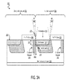
- FIG. 3A is a cross-section diagram illustrating a cross-sectional view of an image sensor according to an embodiment.
- FIG. 3B is a layout diagram illustrating a top view of an image sensor according to an embodiment.
- FIG. 4 is a layout diagram illustrating a top view of an image sensor according to an embodiment.
- FIGs. 5A-5C are cross section diagrams illustrating cross-sectional views of an image sensor according to an embodiment.
- FIG. 6 is a block diagram illustrating elements of an imaging system according to an embodiment.
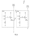
- FIG. 8 is a circuit diagram illustrating elements of pixel circuitry within an imaging array according to an embodiment.
- Embodiments discussed herein variously provide for improved fill factor of an imaging pixel (e.g., the ratio of a photodiode region of a pixel to the total footprint of the pixel) and/or for an improved symmetry of pixels with respect to one another in an image sensor.
- certain embodiments provide for image sensor pixels with self-aligned components to reduce overall pixel size while maintaining large photodiode size and full well capacity, as compared to pixel structures implemented according to conventional techniques. Larger fill factors help to improve the amount of light that is collected by a pixel, while pixel symmetry helps to reduce fixed pattern noise and color shading. Fixed pattern noise can arise from pixel design variations and/or process variations in the pixel array of the image sensor. Color shading can arise from different frequency responses of pixels having different design geometries. Fill factor and/or pixel symmetry may be improved by pixel structures variously implemented by certain embodiments.
- Certain embodiments additionally or alternatively provide image sensor pixels with reduced use of shallow trench isolation ("STI"), as compared to pixel structures implemented according to conventional techniques.
- STI shallow trench isolation
- some embodiments include commonly shared floating diffusion (FD) regions from which pixel signals may be sensed and from which pixels may be reset.
- FD floating diffusion
- an “image sensor pixel' refers to a unit element of an image sensor that generates an electrical signal from an impinging optical signal.
- an “image sensor pixel structure” is a physical structure that includes at least one image sensor pixel and optionally one or more additional structures that manipulate an electrical signal from any of the at least one image sensor pixel.
- An image sensor pixel may include IC structures to operate, for example, in combination with any of a variety of devices such as logic devices, imagers (including CMOS and CCD imagers), and memory (such as DRAM and NOR- and NAND-based flash memory devices). Such devices may, for example, employ transistors for a variety of functions, including switching and amplification of signals.
- Transistors may be formed in integrated circuits by photolithographic processes that are performed on a silicon substrate. Processes to form such transistors may, for example, include operations such as applying a photolithographic resist layer to the substrate, exposing the resist layer to a pattern using light (including deep ultra-violet wavelengths), removing the exposed portions (or non-exposed portions) of the photoresist by etching, and modifying the exposed structure, for example, by depositing or ion implanting additional materials to form various structures for electronic components (including transistors).
- substrate refers to any of a variety of substrates formed using semiconductor material - e.g. based upon silicon, silicon-germanium, germanium, gallium arsenide and/or the like.
- a substrate layer may include such a substrate and one or more structures resulting from operations that have been performed upon the substrate - e.g. such operations forming regions, junctions and/or other structures in the substrate.
- such structures may include one or more of doped semiconductor regions and/or undoped semiconductor regions, epitaxial layers of silicon, and other semiconductor structures formed upon the substrate.
- CMP chemical-mechanical planarization
- additional structures may, for example, be added to the substrate by performing additional processing operations, such as those listed above.
- ion implantation of dopants into selected regions of a substrate may be used to electrically isolate regions disposed within a substrate by exploiting the characteristics of reverse biased diodes.
- Shallow trench isolation (STI) which uses dielectric filled trenches to effect electrical isolation, is another method for isolating regions disposed within a substrate.
- FIG. 1 is a circuit diagram of a four transistor ("4T") unit pixel cell 100 of an imaging sensor according to an embodiment.
- 4T four transistor
- unit pixel cell 100 includes a photodiode (“PD") 110, a transfer transistor (“TX”) 120, a reset transistor (“RST”) 130, a source-follower amplifier (“SF”) 150 and a row select transistor (RS) 160.
- TX 120, RST 130, SF 150 and RS 160 may, for example, include a source, a drain and a gate.
- PD 110 may be electrically coupled to the source of TX 120.
- the drain of TX 120 may be coupled to the drain of RST 130 at a floating drain (“FD”) 140 and to the gate of SF 150.
- the drain of SF 150 may be connected to the source of RS 160.
- the drain of RS 160 may be connected to a column bus 170.
- the source of RST 130 and the source of SF 150 may be connected to a supply voltage Vdd.
- RST 130 When TX 120 is turned off, RST 130 may be turned on by a reset pulse, and FD 140 may be subsequently set to a voltage level of approximately Vdd.
- the voltage at FD 140 may subsequently be amplified by SF 150 - for example, when a row select signal is applied to the gate of RS 160. Subsequently, the reset voltage level of Vdd may be transferred to column bus 170.
- PD 110 may accumulate electrons in response to exposure of pixel cell 100 to electromagnetic energy (represented by arrows 180) - e.g. such as when an image is being taken on a camera and a shutter of the camera is open. This exposure period is also known as an integration period.
- a transfer pulse signal may be applied to the gate of TX 120 to turn on TX 120, thereby allowing accumulated electrons (i.e., charge) in PD 110 to transfer to FD 140.
- SF 150 may convert this charge at FD 140 to a signal voltage.
- an accumulated voltage level at RS 160 may be transferred to column bus 170.
- the voltage on column bus 170 may be sampled at the accumulated voltage level as well as the reset voltage level, such that a difference between the accumulated and reset voltage levels may be identified as a signal voltage which is due to the incidence of electromagnetic energy 180 on photodiode 110.
- the photodiode 110 Before another image is taken during a second integration period, the photodiode 110 itself may be reset. This reset may occur by applying a transfer signal to the gate of TX 120 - e.g. while simultaneously applying a reset signal to the gate of RST 130. PD 110 may thus be reset to approximately Vdd, whereupon and the pixel cell may be ready for a second integration period.
- FWC full well capacity
- Any accumulated charge in PD 110 that was not transferred from PD 110 to FD 140 via TX 120 may remain in PD 110 after reset, and may contribute to image lag (e.g. due to carry-over of remaining charge from a previous integration period to one or more subsequent integration periods, and thus subsequent images).
- image lag e.g. due to carry-over of remaining charge from a previous integration period to one or more subsequent integration periods, and thus subsequent images.
- electrons remaining in PD 100 after reset may effectively reduce the full well capacity (FWC) of the photodiode for subsequent integration periods.
- FWC full well capacity
- Various embodiments provide techniques for improving FWC and/or reducing image lag.
- FIG. 2A shows a top view (also referred to as a "front-side" view) 200a of a conventional pixel structure
- FIG. 2B shows a cross-sectional view 200b of the same pixel structure, the cross-sectional view 200b taken along the line 2B-2B' shown in FIG.2A .
- a p-n-p pinned photodiode is typically constructed using a p-type semiconductor substrate, an n-type well implanted into the p-type substrate, and a p+ layer implanted into the n-type well. This p+ layer acts as the "pin" in a p-n-p photodiode.
- pixel structure 200 includes photodiode 205, a transfer gate 215, a floating drain 220 disposed within a p-type floating drain well 225, and shallow trench isolation (STI) structures 230. For simplicity, only certain elements of the pixel structure associated with portions of transfer gate 215 and photodiode 205 are shown in FIGS. 2A and 2B .
- STI shallow trench isolation
- the portion of pixel structure 200 further includes a p-doped substrate or epitaxially grown layer 245 and an n-type photodiode implant 235 formed within the front-side of p-doped substrate or epitaxially grown layer 245.
- p+ pinned photodiode implant layer 210 is disposed on top of an n-type photodiode implant layer 235.
- a p+ doped layer or substrate extension 213 on the back-side surface of p-type substrate 245 serves as a contact to p-type substrate or epitaxially grown layer 245.
- the electrons flow through the overlap of n-type photodiode implant region 235 and transfer gate 215 and the active channel 260 generated by transfer gate 215 (under transfer gate 215).
- the region of overlap between transfer gate 215 and the n-type photodiode implant region 235 facilitates the transport of electrons. If the region of overlap is too small, or there is no overlap, it is difficult to remove substantially all the electrons from photodiode 205, which results in image lag.
- the overlap of the transfer gate 215 reduces the surface region of photodiode 205, which in turn reduces the light collection region of photodiode region 205.
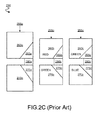
- FIG. 2C illustrates a conventional arrangement 250 of pixel structures which are similar by type to the pixel structure shown in FIGs. 2A and 2B .
- arrangement 250 illustrates various disadvantages of previous image sensor architectures, as compared to those of certain embodiments.
- Arrangement 250 includes pixel pairs 255a, 255b, 255c.
- FIG. 2C illustrates a conventional transfer gate design in a shared pixel architecture. More particularly, the pairs of pixels 255a, 255b, 255c each include a respective floating drain which is shared - e.g. where transfer gates 265a, 275a of pixel pair 255a are both coupled to floating drain 280a, where transfer gates 265b, 275b of pixel pair 255b are both coupled to floating drain 280b and where transfer gates 265c, 275a of pixel pair 255c are both coupled to floating drain 280c.
- Design variation across the pixels in pixel pairs 255a, 255b, 255c may result in variation in the respective fill factors of the pixels.
- pixel pair 255a may have a substantially larger ratio of exposed photodiode region 260a to gate region 265a (or exposed photodiode region 270a to gate region 275a) than the ratio of exposed photodiode region 260b to gate region 265b (or of exposed photodiode region 270b to gate region 275b) of pixel pair 250b.
- design rules often dictate, for example, a minimum space between adjacent transfer gates, a minimum distance from a transfer gate to a closest edge of a photodiode, placement of transfer gate contacts, and/or the like, which tend to reduce the fill factor in pixels.
- design rules according to conventional techniques may require lateral spacing between pixel pairs.
- pixel pair 255b is shown in relation to pixel pair 255c, wherein transfer gate regions 265b, 275b of pixel pair 250b are laterally separated from photodiodes 260c, 270c of pixel pair 250c.
- STI regions which are include in, or which are disposed between, the pixel structures of pixel pairs 250b, 250c.
- conventional pixels include STI regions to separate adjacent photosensitive regions along a horizontal row of pixels as well as between pixels in vertical columns.
- image sensor 380 allows for all, or nearly all, of the area between transfer gates of adjoining pixel structures to be occupied by implant regions of photodiodes and/or allows the elimination of STI structures which might otherwise separate adjacent pixels structures.
- the elimination of STI structures between the laterally spaced pixel elements allows for an increased fill factor.
- elements of a plurality of pixel structures reside within in a region of a semiconductor layer, wherein one or more STI structures and one or more floating diffusion structures define a perimeter of that region of the semiconductor layer.
- Such a plurality of pixel structures may further include one or more component elements which are disposed on the region - e.g. including one or more transfer gates adjoining the surface of the semiconductor layer.
- the region of the semiconductor layer which is bounded by the one or more STI structures and one or more floating diffusion structures may, for example, include elements of different respective pixel structures which are not separated from one another by any STI structure.
- the plurality of pixel structures having elements within the region of the semiconductor layer may share the one or more floating diffusion structures with one or more pixel structures which reside outside of that region of the semiconductor layer.
- FIG. 4 A top view illustrating portions of 3 pixel elements of pixel array structure 400 is shown in FIG. 4 , where each pixel in the group (e.g. row) has a single photodiode, a single channel stopper, a single transfer gate and a shared floating diffusion per pixel.
- FIG. 4 illustrates a first pixel element 401 having a photodiode region 460, where an STI isolation region 410 is disposed along three of the sides of the first photodiode region 460, while a first transfer gate 420 and first channel stopper 430 are arranged along a fourth side of the first photodiode region 460.
- the first transfer gate 420 has one associated first floating diffusion 450.
- the first floating diffusion region 450 is disposed between vertically adjacent transfer gates 420 (in pixel element row below pixel row 400 and not shown) and can be shared as discussed above with respect to FIG. 3C .
- photoelectrons generated and collected in the photodiode are transferred under the transfer gate to the floating diffusion region during imaging.
- the channel stopper prevents signal carrier exchange (cross talk) between adjacent pixel elements.
- FIG. 4 also illustrates a second pixel element 402 having a second photodiode region 460 that has STI isolation regions 410 along two of the sides of the second photodiode region 460.
- a second transfer gate 420 and channel stopper 430 are arranged along a third side of the second photodiode region 460.
- the second photodiode region is arranged adjacent to the first transfer gate 420 and first channel stopper of the first pixel element.
- the second transfer gate 420 has one associated second floating diffusion 450.
- the second floating diffusion region 450 is disposed between vertically adjacent transfer gates 420 (in a pixel element row below pixel row 400 and not shown) and can be shared as discussed above with respect to FIG. 3C .
- FIG. 4 also illustrates a third pixel element 403 having a third photodiode region 460, a third transfer gate 420, and a third channel stopper 430.
- STI isolation regions 410 lie along three of the sides of the third pixel element 403, while on the fourth side of the third pixel element the third photodiode region 460 is arranged adjacent to the second transfer gate 420 and second channel stopper 430 of the second pixel element along the side of the second pixel element in common with the third pixel element.
- the third transfer gate 420 has one associated third floating diffusion 450.
- the third floating diffusion region 450 is disposed between vertically adjacent transfer gates 420 (in a pixel element row below pixel row 400 and not shown) and can be shared as discussed above with respect to FIG. 3C .
- Cross section view lines A-A, B-B', and C-C' as illustrated in FIG. 4 are discussed below.
- an electrode of polysilicon transfer gate 420 may be of sufficient thickness that its height acts as a shadow mask to various illustrated ion implants - e.g. implants for p-type implant regions 440.
- the use of the angled ion implant to form an offset of photodiode regions 460 from opposite edges of respective transfer gates 420 helps implement efficient photodiode structures disclosed herein.
- FIG. 5B illustrates a second cross-section view 510 (view B-B') of FIG. 4 .
- cross-section view 510 shows the n-type photodiode region 460 overlaid by the p-type pinning region 440 and two STI regions 410 on either side.
- the photodiode regions 440, 460 occupy a p-type doped substrate (or p-type well).
- FIG. 6 illustrates elements of an imaging system 600 according to an embodiment.
- Imaging system 600 may include optics 601 - e.g. any of a variety of combinations of refractive, diffractive and/or reflective optical elements - and an image sensor 602 coupled thereto.
- optics 601 may focus an image onto pixels in a pixel array 604 of image sensor 602.
- Pixel array 604 may capture the image for other circuitry of imaging system 600 to process - e.g. to generate pixel data representing the image.
- Image sensor 602 may comprise, for example, pixel array 604 and a signal reading and processing circuit 610 coupled thereto.
- image sensor 602 is a backside illuminated (BSI) image sensor including a pixel array 604 having a plurality of pixels arranged in rows 606 and columns 608.
- image sensor 602 may be a front side illuminated (FSI) image sensor or an image sensor that combines BSI with FSI.
- BSI backside illuminated
- FSI front side illuminated
- one or more of the pixels in pixel array 604 may comprise an arrangement such as that shown in FIGs. 4 and 5A-5C .
- one or more pixels in pixel array 604 may comprise any of various other pixel structure arrangements discussed herein.
- Pixel array 604 is merely illustrative, and is not limiting on certain embodiments. By way of illustration and not limitation, pixel array 604 may have any of a variety of additional or alternative rows and/or columns.
- pixels in pixel array 604 may capture incident light (i.e., photons) during a certain exposure period and convert the collected photons into an electrical charge.
- the electrical charge generated by one of such pixels may be read out as an analog signal - e.g. where a characteristic of the analog signal such as its charge, voltage or current may be representative of an intensity of light that was incident on that pixel during the exposure period.
- pixel array 604 may include a color image sensor - e.g. including red, green, and blue pixels designed to capture images in the visible portion of the spectrum - a black-and-white image sensor and/or an image sensor designed to capture images in the invisible portion of the spectrum, such as infra-red or ultraviolet.
- a color image sensor e.g. including red, green, and blue pixels designed to capture images in the visible portion of the spectrum - a black-and-white image sensor and/or an image sensor designed to capture images in the invisible portion of the spectrum, such as infra-red or ultraviolet.
- Imaging system 600 may include a signal conditioner 612 - e.g. coupled to image sensor 602 - to receive and condition analog signals from pixel array 604 and/or reading and processing circuit 610.
- signal conditioner 612 can include various components for conditioning analog signals. Examples of components that can be found in the signal conditioner 612 include filters, amplifiers, offset circuits, automatic gain control, etc. In an embodiment where signal conditioner 612 includes only some of these elements and performs only some conditioning functions, the remaining functions may be performed by one or more other components such as circuit 610 or DSP 616.
- an analog-to-digital converter (ADC) 614 may be coupled to signal conditioner 612 to receive conditioned analog signals - e.g. the conditioned signals corresponding to each pixel in pixel array 604 from signal conditioner 612 - and to convert these analog signals into digital values.
- ADC analog-to-digital converter
- Imaging system 600 may include a DSP 616 - e.g. coupled to analog-to-digital converter 614 - to receive digitized pixel data from ADC 614 and to process the digital data to produce a final digital image.
- DSP 616 may, for example, include a processor and an internal memory (not shown) in which it can store and retrieve data. After the image is processed by DSP 616, it can be output to one or both of a storage unit 618 such as a flash memory or an optical or magnetic storage unit and a display unit 620 such as an LCD screen.
- FIG. 7 shows a block diagram of an exemplary design flow 700 used for example, in semiconductor design and manufacturing of the image sensor pixel array and semiconductor circuits according to the present invention.
- Design structure 720 may include an input to a design process 710, wherein design structure 720 comprises data describing structures according to an embodiment - such as those shown in any of FIGS. 3A-3C , 4 and 5A-5C - in the form of schematics or hardware description language (HDL; e.g., Verilog, VHDL, C, etc.).
- the design structure 720 may be a text file or a graphical representation of an embodiment of the invention, e.g. as shown in some or all of FIGS. 3A-3C , 4 and 5A-5C .
- a machine readable storage medium embodying a design structure may be provided.
- the design structure may include first data representing a first pixel structure including a first photodiode in a semiconductor layer, the first photodiode having a first implant region, wherein a skew of the first implant region corresponds to a first implant angle.
- the first data representing a first pixel structure may further represent both a second implant region at least partially overlapping the first implant region and a first transfer gate adjoining a surface of the semiconductor layer.
- the design process 710 may include using a variety of inputs; for example, inputs from library elements 730 which may house a set of commonly used elements, circuits, and devices, including models, layouts, and symbolic representations, for a given manufacturing technology (e.g., different technology nodes such as 32nm, 45nm, and 90nm, etc.), design specifications 740, characterization data 750, verification data 760, design rules 770, and test data files 785 (which may include, for example, standard circuit design processes such as timing analysis, verification, design rule checking, place and route operations, etc.)
- library elements 730 which may house a set of commonly used elements, circuits, and devices, including models, layouts, and symbolic representations, for a given manufacturing technology (e.g., different technology nodes such as 32nm, 45nm, and 90nm, etc.), design specifications 740, characterization data 750, verification data 760, design rules 770, and test data files 785 (which may include, for example, standard circuit design processes such as
- the TX signal, the RST signal, the SEL signal, VDD, and ground may be routed in imaging pixel circuitry 800 by way of metal interconnect layers.
- transistors T1, T2, T3, and T4 may be connected as shown in FIG. 8 by way of metal interconnect layers.
Landscapes
- Solid State Image Pick-Up Elements (AREA)
- Transforming Light Signals Into Electric Signals (AREA)
Applications Claiming Priority (1)
| Application Number | Priority Date | Filing Date | Title |
|---|---|---|---|
| US13/288,880 US8804021B2 (en) | 2011-11-03 | 2011-11-03 | Method, apparatus and system for providing improved full well capacity in an image sensor pixel |
Publications (3)
| Publication Number | Publication Date |
|---|---|
| EP2590220A2 true EP2590220A2 (de) | 2013-05-08 |
| EP2590220A3 EP2590220A3 (de) | 2013-08-28 |
| EP2590220B1 EP2590220B1 (de) | 2018-06-27 |
Family
ID=47227478
Family Applications (1)
| Application Number | Title | Priority Date | Filing Date |
|---|---|---|---|
| EP12190843.8A Active EP2590220B1 (de) | 2011-11-03 | 2012-10-31 | Verfahren, Vorrichtung und System zur Bereitstellung verbesserter Full-Well-Kapazität in einem Bildsensorpixel |
Country Status (4)
| Country | Link |
|---|---|
| US (1) | US8804021B2 (de) |
| EP (1) | EP2590220B1 (de) |
| CN (1) | CN103094292B (de) |
| TW (1) | TWI520318B (de) |
Cited By (1)
| Publication number | Priority date | Publication date | Assignee | Title |
|---|---|---|---|---|
| EP3706170A4 (de) * | 2017-10-31 | 2021-08-04 | Stanley Electric Co., Ltd. | Bildaufnahmevorrichtung und bildaufnahmeelement |
Families Citing this family (49)
| Publication number | Priority date | Publication date | Assignee | Title |
|---|---|---|---|---|
| US5167750A (en) * | 1989-02-08 | 1992-12-01 | Stahl's Special Projects, Inc. | Heat sealing machine |
| US8883544B2 (en) * | 2012-05-04 | 2014-11-11 | Taiwan Semiconductor Manufacturing Company, Ltd. | Method of forming an image device |
| KR102034482B1 (ko) | 2013-03-04 | 2019-10-21 | 삼성전자주식회사 | 이미지 센서 및 이의 형성 방법 |
| JP2014199898A (ja) * | 2013-03-11 | 2014-10-23 | ソニー株式会社 | 固体撮像素子および製造方法、並びに、電子機器 |
| CN106456272B (zh) * | 2014-03-17 | 2020-03-31 | 直观外科手术操作公司 | 包括非白光总体照明器的外科手术系统 |
| EP3471402B1 (de) | 2014-08-08 | 2023-05-31 | Quantum-Si Incorporated | Integrierte vorrichtung zur temporären gruppierung von empfangenen photonen |
| CN104143558B (zh) * | 2014-08-15 | 2018-03-27 | 北京思比科微电子技术股份有限公司 | 一种提高阱容量的图像传感器像素及其制作方法 |
| US9111993B1 (en) * | 2014-08-21 | 2015-08-18 | Omnivision Technologies, Inc. | Conductive trench isolation |
| JP6362478B2 (ja) * | 2014-08-27 | 2018-07-25 | ルネサスエレクトロニクス株式会社 | 半導体装置の製造方法および半導体装置 |
| KR102301778B1 (ko) | 2014-08-28 | 2021-09-13 | 삼성전자주식회사 | 이미지 센서, 및 상기 이미지 센서의 픽셀 |
| US9923003B2 (en) * | 2015-06-30 | 2018-03-20 | Microsoft Technology Licensing, Llc | CMOS image sensor with a reduced likelihood of an induced electric field in the epitaxial layer |
| JP6707662B2 (ja) * | 2016-01-15 | 2020-06-10 | インヴィサージ テクノロジーズ インコーポレイテッド | 拡張ダイナミックレンジを有する画像センサ |
| US9930281B2 (en) * | 2016-01-20 | 2018-03-27 | Semiconductor Components Industries, Llc | Image sensors having photodiode regions implanted from multiple sides of a substrate |
| US10917625B1 (en) | 2016-10-20 | 2021-02-09 | Facebook Technologies, Llc | Time multiplexed dual-band sensor |
| CA3047826A1 (en) * | 2016-12-22 | 2018-06-28 | Quantum-Si Incorporated | Integrated photodetector with direct binning pixel |
| FR3065836B1 (fr) | 2017-04-28 | 2020-02-07 | Commissariat A L'energie Atomique Et Aux Energies Alternatives | Zone de stockage pour un pixel d'une matrice d'image |
| US10686996B2 (en) | 2017-06-26 | 2020-06-16 | Facebook Technologies, Llc | Digital pixel with extended dynamic range |
| US10419701B2 (en) | 2017-06-26 | 2019-09-17 | Facebook Technologies, Llc | Digital pixel image sensor |
| JP6985054B2 (ja) * | 2017-08-01 | 2021-12-22 | スタンレー電気株式会社 | 撮像装置 |
| DE102018106267B4 (de) | 2017-08-15 | 2025-04-30 | Taiwan Semiconductor Manufacturing Co. Ltd. | Neuartiger bildsensor |
| US10777591B2 (en) | 2017-08-15 | 2020-09-15 | Taiwan Semiconductor Manufacturing Co., Ltd. | Image sensor device |
| US10598546B2 (en) | 2017-08-17 | 2020-03-24 | Facebook Technologies, Llc | Detecting high intensity light in photo sensor |
| US11393867B2 (en) | 2017-12-06 | 2022-07-19 | Facebook Technologies, Llc | Multi-photodiode pixel cell |
| US10969273B2 (en) | 2018-03-19 | 2021-04-06 | Facebook Technologies, Llc | Analog-to-digital converter having programmable quantization resolution |
| US11004881B2 (en) | 2018-04-03 | 2021-05-11 | Facebook Technologies, Llc | Global shutter image sensor |
| US10923523B2 (en) | 2018-04-16 | 2021-02-16 | Facebook Technologies, Llc | Multi-photodiode pixel cell |
| US11233085B2 (en) | 2018-05-09 | 2022-01-25 | Facebook Technologies, Llc | Multi-photo pixel cell having vertical gate structure |
| US10903260B2 (en) * | 2018-06-11 | 2021-01-26 | Facebook Technologies, Llc | Multi-photodiode pixel cell |
| US11089210B2 (en) | 2018-06-11 | 2021-08-10 | Facebook Technologies, Llc | Configurable image sensor |
| US11089241B2 (en) | 2018-06-11 | 2021-08-10 | Facebook Technologies, Llc | Pixel cell with multiple photodiodes |
| US11906353B2 (en) | 2018-06-11 | 2024-02-20 | Meta Platforms Technologies, Llc | Digital pixel with extended dynamic range |
| CN119364214A (zh) | 2018-06-22 | 2025-01-24 | 宽腾矽公司 | 具有不同检测时间的电荷存储仓的集成光电检测器 |
| US11463636B2 (en) | 2018-06-27 | 2022-10-04 | Facebook Technologies, Llc | Pixel sensor having multiple photodiodes |
| US10897586B2 (en) | 2018-06-28 | 2021-01-19 | Facebook Technologies, Llc | Global shutter image sensor |
| US10931884B2 (en) | 2018-08-20 | 2021-02-23 | Facebook Technologies, Llc | Pixel sensor having adaptive exposure time |
| US11956413B2 (en) | 2018-08-27 | 2024-04-09 | Meta Platforms Technologies, Llc | Pixel sensor having multiple photodiodes and shared comparator |
| US11595602B2 (en) | 2018-11-05 | 2023-02-28 | Meta Platforms Technologies, Llc | Image sensor post processing |
| US11102430B2 (en) | 2018-12-10 | 2021-08-24 | Facebook Technologies, Llc | Pixel sensor having multiple photodiodes |
| US11218660B1 (en) | 2019-03-26 | 2022-01-04 | Facebook Technologies, Llc | Pixel sensor having shared readout structure |
| US11943561B2 (en) | 2019-06-13 | 2024-03-26 | Meta Platforms Technologies, Llc | Non-linear quantization at pixel sensor |
| US11936998B1 (en) | 2019-10-17 | 2024-03-19 | Meta Platforms Technologies, Llc | Digital pixel sensor having extended dynamic range |
| US11902685B1 (en) | 2020-04-28 | 2024-02-13 | Meta Platforms Technologies, Llc | Pixel sensor having hierarchical memory |
| US11910114B2 (en) | 2020-07-17 | 2024-02-20 | Meta Platforms Technologies, Llc | Multi-mode image sensor |
| US11956560B2 (en) | 2020-10-09 | 2024-04-09 | Meta Platforms Technologies, Llc | Digital pixel sensor having reduced quantization operation |
| CN114388536A (zh) * | 2020-10-21 | 2022-04-22 | 格科微电子(上海)有限公司 | 图像传感器形成方法及图像传感器 |
| US12022218B2 (en) | 2020-12-29 | 2024-06-25 | Meta Platforms Technologies, Llc | Digital image sensor using a single-input comparator based quantizer |
| CN115831991B (zh) | 2021-09-17 | 2026-03-17 | 意法半导体(克洛尔2)公司 | 图像和深度像素 |
| FR3127329B1 (fr) * | 2021-09-17 | 2024-01-26 | St Microelectronics Crolles 2 Sas | Pixel d'image et de profondeur |
| US20260052784A1 (en) * | 2024-08-19 | 2026-02-19 | Raytheon Company | Pixel implant geometries for high-performance photodetectors |
Family Cites Families (10)
| Publication number | Priority date | Publication date | Assignee | Title |
|---|---|---|---|---|
| US5851886A (en) * | 1995-10-23 | 1998-12-22 | Advanced Micro Devices, Inc. | Method of large angle tilt implant of channel region |
| US6690423B1 (en) * | 1998-03-19 | 2004-02-10 | Kabushiki Kaisha Toshiba | Solid-state image pickup apparatus |
| US6465820B1 (en) | 1998-09-16 | 2002-10-15 | Dalsa, Inc. | CMOS compatible single phase CCD charge transfer device |
| JP2001308304A (ja) | 2000-04-19 | 2001-11-02 | Sony Corp | 固体撮像素子の製造方法 |
| US7420233B2 (en) * | 2003-10-22 | 2008-09-02 | Micron Technology, Inc. | Photodiode for improved transfer gate leakage |
| KR100808950B1 (ko) * | 2007-01-30 | 2008-03-04 | 삼성전자주식회사 | 씨모스 이미지 센서 및 그 제조 방법 |
| US7459668B2 (en) * | 2007-03-06 | 2008-12-02 | Micron Technology, Inc. | Method, apparatus, and system to reduce ground resistance in a pixel array |
| JP2010161236A (ja) | 2009-01-08 | 2010-07-22 | Canon Inc | 光電変換装置の製造方法 |
| US8405751B2 (en) | 2009-08-03 | 2013-03-26 | International Business Machines Corporation | Image sensor pixel structure employing a shared floating diffusion |
| US8658956B2 (en) * | 2009-10-20 | 2014-02-25 | Omnivision Technologies, Inc. | Trench transfer gate for increased pixel fill factor |
-
2011
- 2011-11-03 US US13/288,880 patent/US8804021B2/en active Active
-
2012
- 2012-10-31 EP EP12190843.8A patent/EP2590220B1/de active Active
- 2012-11-01 TW TW101140615A patent/TWI520318B/zh active
- 2012-11-02 CN CN201210432093.6A patent/CN103094292B/zh active Active
Non-Patent Citations (1)
| Title |
|---|
| None |
Cited By (1)
| Publication number | Priority date | Publication date | Assignee | Title |
|---|---|---|---|---|
| EP3706170A4 (de) * | 2017-10-31 | 2021-08-04 | Stanley Electric Co., Ltd. | Bildaufnahmevorrichtung und bildaufnahmeelement |
Also Published As
| Publication number | Publication date |
|---|---|
| HK1183162A1 (zh) | 2013-12-13 |
| TWI520318B (zh) | 2016-02-01 |
| EP2590220A3 (de) | 2013-08-28 |
| CN103094292B (zh) | 2015-12-09 |
| CN103094292A (zh) | 2013-05-08 |
| US20130113969A1 (en) | 2013-05-09 |
| US8804021B2 (en) | 2014-08-12 |
| EP2590220B1 (de) | 2018-06-27 |
| TW201327793A (zh) | 2013-07-01 |
Similar Documents
| Publication | Publication Date | Title |
|---|---|---|
| EP2590220B1 (de) | Verfahren, Vorrichtung und System zur Bereitstellung verbesserter Full-Well-Kapazität in einem Bildsensorpixel | |
| CN206742242U (zh) | 成像传感器和成像像素 | |
| US8658956B2 (en) | Trench transfer gate for increased pixel fill factor | |
| US9318520B2 (en) | Solid-state image sensing device manufacturing method and solid-state image sensing device | |
| US7696597B2 (en) | Split transfer gate for dark current suppression in an imager pixel | |
| US8916917B2 (en) | Solid-state imaging device | |
| CN110581147A (zh) | 具有多光电二极管图像像素和竖直转移门的图像传感器 | |
| US7898010B2 (en) | Transparent conductor based pinned photodiode | |
| US20110249163A1 (en) | Photoelectric conversion device and camera | |
| CN101939982A (zh) | 具有全域快门及储存电容的背侧照明影像传感器 | |
| EP4075521A1 (de) | Festkörperbildsensor und elektronische vorrichtung | |
| CN102460702A (zh) | 具有偏压材料及背侧阱的成像器 | |
| TWI413246B (zh) | 在一互補式金氧半導體像素中之半島形傳送閘 | |
| US12262563B2 (en) | Pixel cell having anti-blooming structure and image sensor | |
| CN103581580B (zh) | 用于低暗电流cmos像素单元的接地触点结构 | |
| TWI525801B (zh) | 具有經摻雜之傳輸閘極的影像感測器 | |
| US8462239B2 (en) | Solid-state imaging device and electronic imaging device having multi-stage element isolation layer | |
| HK1183162B (en) | Method, apparatus and system for providing improved full well capacity in an image sensor pixel | |
| US20120080731A1 (en) | Photodetector isolation in image sensors | |
| CN120075641A (zh) | 具有沟槽存储栅极的背照式全局快门图像传感器 | |
| HK1170846A (en) | Photodetector isolation in image sensors | |
| HK1170845A (en) | Method for forming photodetector isolation in imagers |
Legal Events
| Date | Code | Title | Description |
|---|---|---|---|
| PUAI | Public reference made under article 153(3) epc to a published international application that has entered the european phase |
Free format text: ORIGINAL CODE: 0009012 |
|
| AK | Designated contracting states |
Kind code of ref document: A2 Designated state(s): AL AT BE BG CH CY CZ DE DK EE ES FI FR GB GR HR HU IE IS IT LI LT LU LV MC MK MT NL NO PL PT RO RS SE SI SK SM TR |
|
| AX | Request for extension of the european patent |
Extension state: BA ME |
|
| PUAL | Search report despatched |
Free format text: ORIGINAL CODE: 0009013 |
|
| AK | Designated contracting states |
Kind code of ref document: A3 Designated state(s): AL AT BE BG CH CY CZ DE DK EE ES FI FR GB GR HR HU IE IS IT LI LT LU LV MC MK MT NL NO PL PT RO RS SE SI SK SM TR |
|
| AX | Request for extension of the european patent |
Extension state: BA ME |
|
| RIC1 | Information provided on ipc code assigned before grant |
Ipc: H01L 27/146 20060101AFI20130722BHEP |
|
| 17P | Request for examination filed |
Effective date: 20140227 |
|
| RBV | Designated contracting states (corrected) |
Designated state(s): AL AT BE BG CH CY CZ DE DK EE ES FI FR GB GR HR HU IE IS IT LI LT LU LV MC MK MT NL NO PL PT RO RS SE SI SK SM TR |
|
| 17Q | First examination report despatched |
Effective date: 20161215 |
|
| GRAP | Despatch of communication of intention to grant a patent |
Free format text: ORIGINAL CODE: EPIDOSNIGR1 |
|
| INTG | Intention to grant announced |
Effective date: 20171208 |
|
| GRAS | Grant fee paid |
Free format text: ORIGINAL CODE: EPIDOSNIGR3 |
|
| GRAA | (expected) grant |
Free format text: ORIGINAL CODE: 0009210 |
|
| AK | Designated contracting states |
Kind code of ref document: B1 Designated state(s): AL AT BE BG CH CY CZ DE DK EE ES FI FR GB GR HR HU IE IS IT LI LT LU LV MC MK MT NL NO PL PT RO RS SE SI SK SM TR |
|
| REG | Reference to a national code |
Ref country code: GB Ref legal event code: FG4D |
|
| REG | Reference to a national code |
Ref country code: AT Ref legal event code: REF Ref document number: 1013062 Country of ref document: AT Kind code of ref document: T Effective date: 20180715 |
|
| REG | Reference to a national code |
Ref country code: IE Ref legal event code: FG4D |
|
| REG | Reference to a national code |
Ref country code: DE Ref legal event code: R096 Ref document number: 602012047785 Country of ref document: DE |
|
| REG | Reference to a national code |
Ref country code: FR Ref legal event code: PLFP Year of fee payment: 7 |
|
| PG25 | Lapsed in a contracting state [announced via postgrant information from national office to epo] |
Ref country code: NO Free format text: LAPSE BECAUSE OF FAILURE TO SUBMIT A TRANSLATION OF THE DESCRIPTION OR TO PAY THE FEE WITHIN THE PRESCRIBED TIME-LIMIT Effective date: 20180927 Ref country code: SE Free format text: LAPSE BECAUSE OF FAILURE TO SUBMIT A TRANSLATION OF THE DESCRIPTION OR TO PAY THE FEE WITHIN THE PRESCRIBED TIME-LIMIT Effective date: 20180627 Ref country code: BG Free format text: LAPSE BECAUSE OF FAILURE TO SUBMIT A TRANSLATION OF THE DESCRIPTION OR TO PAY THE FEE WITHIN THE PRESCRIBED TIME-LIMIT Effective date: 20180927 Ref country code: FI Free format text: LAPSE BECAUSE OF FAILURE TO SUBMIT A TRANSLATION OF THE DESCRIPTION OR TO PAY THE FEE WITHIN THE PRESCRIBED TIME-LIMIT Effective date: 20180627 Ref country code: LT Free format text: LAPSE BECAUSE OF FAILURE TO SUBMIT A TRANSLATION OF THE DESCRIPTION OR TO PAY THE FEE WITHIN THE PRESCRIBED TIME-LIMIT Effective date: 20180627 |
|
| REG | Reference to a national code |
Ref country code: NL Ref legal event code: MP Effective date: 20180627 |
|
| REG | Reference to a national code |
Ref country code: LT Ref legal event code: MG4D |
|
| PG25 | Lapsed in a contracting state [announced via postgrant information from national office to epo] |
Ref country code: LV Free format text: LAPSE BECAUSE OF FAILURE TO SUBMIT A TRANSLATION OF THE DESCRIPTION OR TO PAY THE FEE WITHIN THE PRESCRIBED TIME-LIMIT Effective date: 20180627 Ref country code: HR Free format text: LAPSE BECAUSE OF FAILURE TO SUBMIT A TRANSLATION OF THE DESCRIPTION OR TO PAY THE FEE WITHIN THE PRESCRIBED TIME-LIMIT Effective date: 20180627 Ref country code: GR Free format text: LAPSE BECAUSE OF FAILURE TO SUBMIT A TRANSLATION OF THE DESCRIPTION OR TO PAY THE FEE WITHIN THE PRESCRIBED TIME-LIMIT Effective date: 20180928 Ref country code: RS Free format text: LAPSE BECAUSE OF FAILURE TO SUBMIT A TRANSLATION OF THE DESCRIPTION OR TO PAY THE FEE WITHIN THE PRESCRIBED TIME-LIMIT Effective date: 20180627 |
|
| REG | Reference to a national code |
Ref country code: AT Ref legal event code: MK05 Ref document number: 1013062 Country of ref document: AT Kind code of ref document: T Effective date: 20180627 |
|
| PG25 | Lapsed in a contracting state [announced via postgrant information from national office to epo] |
Ref country code: NL Free format text: LAPSE BECAUSE OF FAILURE TO SUBMIT A TRANSLATION OF THE DESCRIPTION OR TO PAY THE FEE WITHIN THE PRESCRIBED TIME-LIMIT Effective date: 20180627 |
|
| PG25 | Lapsed in a contracting state [announced via postgrant information from national office to epo] |
Ref country code: IS Free format text: LAPSE BECAUSE OF FAILURE TO SUBMIT A TRANSLATION OF THE DESCRIPTION OR TO PAY THE FEE WITHIN THE PRESCRIBED TIME-LIMIT Effective date: 20181027 Ref country code: AT Free format text: LAPSE BECAUSE OF FAILURE TO SUBMIT A TRANSLATION OF THE DESCRIPTION OR TO PAY THE FEE WITHIN THE PRESCRIBED TIME-LIMIT Effective date: 20180627 Ref country code: EE Free format text: LAPSE BECAUSE OF FAILURE TO SUBMIT A TRANSLATION OF THE DESCRIPTION OR TO PAY THE FEE WITHIN THE PRESCRIBED TIME-LIMIT Effective date: 20180627 Ref country code: PL Free format text: LAPSE BECAUSE OF FAILURE TO SUBMIT A TRANSLATION OF THE DESCRIPTION OR TO PAY THE FEE WITHIN THE PRESCRIBED TIME-LIMIT Effective date: 20180627 Ref country code: RO Free format text: LAPSE BECAUSE OF FAILURE TO SUBMIT A TRANSLATION OF THE DESCRIPTION OR TO PAY THE FEE WITHIN THE PRESCRIBED TIME-LIMIT Effective date: 20180627 Ref country code: CZ Free format text: LAPSE BECAUSE OF FAILURE TO SUBMIT A TRANSLATION OF THE DESCRIPTION OR TO PAY THE FEE WITHIN THE PRESCRIBED TIME-LIMIT Effective date: 20180627 Ref country code: SK Free format text: LAPSE BECAUSE OF FAILURE TO SUBMIT A TRANSLATION OF THE DESCRIPTION OR TO PAY THE FEE WITHIN THE PRESCRIBED TIME-LIMIT Effective date: 20180627 |
|
| PG25 | Lapsed in a contracting state [announced via postgrant information from national office to epo] |
Ref country code: SM Free format text: LAPSE BECAUSE OF FAILURE TO SUBMIT A TRANSLATION OF THE DESCRIPTION OR TO PAY THE FEE WITHIN THE PRESCRIBED TIME-LIMIT Effective date: 20180627 Ref country code: IT Free format text: LAPSE BECAUSE OF FAILURE TO SUBMIT A TRANSLATION OF THE DESCRIPTION OR TO PAY THE FEE WITHIN THE PRESCRIBED TIME-LIMIT Effective date: 20180627 Ref country code: ES Free format text: LAPSE BECAUSE OF FAILURE TO SUBMIT A TRANSLATION OF THE DESCRIPTION OR TO PAY THE FEE WITHIN THE PRESCRIBED TIME-LIMIT Effective date: 20180627 |
|
| REG | Reference to a national code |
Ref country code: DE Ref legal event code: R097 Ref document number: 602012047785 Country of ref document: DE |
|
| PLBE | No opposition filed within time limit |
Free format text: ORIGINAL CODE: 0009261 |
|
| STAA | Information on the status of an ep patent application or granted ep patent |
Free format text: STATUS: NO OPPOSITION FILED WITHIN TIME LIMIT |
|
| PG25 | Lapsed in a contracting state [announced via postgrant information from national office to epo] |
Ref country code: DK Free format text: LAPSE BECAUSE OF FAILURE TO SUBMIT A TRANSLATION OF THE DESCRIPTION OR TO PAY THE FEE WITHIN THE PRESCRIBED TIME-LIMIT Effective date: 20180627 |
|
| 26N | No opposition filed |
Effective date: 20190328 |
|
| REG | Reference to a national code |
Ref country code: BE Ref legal event code: MM Effective date: 20181031 |
|
| PG25 | Lapsed in a contracting state [announced via postgrant information from national office to epo] |
Ref country code: LU Free format text: LAPSE BECAUSE OF NON-PAYMENT OF DUE FEES Effective date: 20181031 Ref country code: MC Free format text: LAPSE BECAUSE OF FAILURE TO SUBMIT A TRANSLATION OF THE DESCRIPTION OR TO PAY THE FEE WITHIN THE PRESCRIBED TIME-LIMIT Effective date: 20180627 |
|
| REG | Reference to a national code |
Ref country code: IE Ref legal event code: MM4A |
|
| PG25 | Lapsed in a contracting state [announced via postgrant information from national office to epo] |
Ref country code: BE Free format text: LAPSE BECAUSE OF NON-PAYMENT OF DUE FEES Effective date: 20181031 Ref country code: SI Free format text: LAPSE BECAUSE OF FAILURE TO SUBMIT A TRANSLATION OF THE DESCRIPTION OR TO PAY THE FEE WITHIN THE PRESCRIBED TIME-LIMIT Effective date: 20180627 |
|
| PG25 | Lapsed in a contracting state [announced via postgrant information from national office to epo] |
Ref country code: IE Free format text: LAPSE BECAUSE OF NON-PAYMENT OF DUE FEES Effective date: 20181031 |
|
| PG25 | Lapsed in a contracting state [announced via postgrant information from national office to epo] |
Ref country code: AL Free format text: LAPSE BECAUSE OF FAILURE TO SUBMIT A TRANSLATION OF THE DESCRIPTION OR TO PAY THE FEE WITHIN THE PRESCRIBED TIME-LIMIT Effective date: 20180627 |
|
| PG25 | Lapsed in a contracting state [announced via postgrant information from national office to epo] |
Ref country code: MT Free format text: LAPSE BECAUSE OF NON-PAYMENT OF DUE FEES Effective date: 20181031 |
|
| PG25 | Lapsed in a contracting state [announced via postgrant information from national office to epo] |
Ref country code: TR Free format text: LAPSE BECAUSE OF FAILURE TO SUBMIT A TRANSLATION OF THE DESCRIPTION OR TO PAY THE FEE WITHIN THE PRESCRIBED TIME-LIMIT Effective date: 20180627 |
|
| PG25 | Lapsed in a contracting state [announced via postgrant information from national office to epo] |
Ref country code: PT Free format text: LAPSE BECAUSE OF FAILURE TO SUBMIT A TRANSLATION OF THE DESCRIPTION OR TO PAY THE FEE WITHIN THE PRESCRIBED TIME-LIMIT Effective date: 20180627 |
|
| PG25 | Lapsed in a contracting state [announced via postgrant information from national office to epo] |
Ref country code: HU Free format text: LAPSE BECAUSE OF FAILURE TO SUBMIT A TRANSLATION OF THE DESCRIPTION OR TO PAY THE FEE WITHIN THE PRESCRIBED TIME-LIMIT; INVALID AB INITIO Effective date: 20121031 Ref country code: CY Free format text: LAPSE BECAUSE OF FAILURE TO SUBMIT A TRANSLATION OF THE DESCRIPTION OR TO PAY THE FEE WITHIN THE PRESCRIBED TIME-LIMIT Effective date: 20180627 Ref country code: MK Free format text: LAPSE BECAUSE OF NON-PAYMENT OF DUE FEES Effective date: 20180627 |
|
| P01 | Opt-out of the competence of the unified patent court (upc) registered |
Effective date: 20230420 |
|
| REG | Reference to a national code |
Ref country code: DE Ref legal event code: R079 Ref document number: 602012047785 Country of ref document: DE Free format text: PREVIOUS MAIN CLASS: H01L0027146000 Ipc: H10F0039180000 |
|
| PGFP | Annual fee paid to national office [announced via postgrant information from national office to epo] |
Ref country code: GB Payment date: 20250911 Year of fee payment: 14 |
|
| PGFP | Annual fee paid to national office [announced via postgrant information from national office to epo] |
Ref country code: FR Payment date: 20250912 Year of fee payment: 14 |
|
| REG | Reference to a national code |
Ref country code: CH Ref legal event code: U11 Free format text: ST27 STATUS EVENT CODE: U-0-0-U10-U11 (AS PROVIDED BY THE NATIONAL OFFICE) Effective date: 20251101 |
|
| PGFP | Annual fee paid to national office [announced via postgrant information from national office to epo] |
Ref country code: DE Payment date: 20250912 Year of fee payment: 14 |
|
| PGFP | Annual fee paid to national office [announced via postgrant information from national office to epo] |
Ref country code: CH Payment date: 20251101 Year of fee payment: 14 |