EP2587486B1 - Time division multiplexed multiport memory - Google Patents
Time division multiplexed multiport memory Download PDFInfo
- Publication number
- EP2587486B1 EP2587486B1 EP12189371.3A EP12189371A EP2587486B1 EP 2587486 B1 EP2587486 B1 EP 2587486B1 EP 12189371 A EP12189371 A EP 12189371A EP 2587486 B1 EP2587486 B1 EP 2587486B1
- Authority
- EP
- European Patent Office
- Prior art keywords
- port
- memory
- signal
- memory access
- edge
- Prior art date
- Legal status (The legal status is an assumption and is not a legal conclusion. Google has not performed a legal analysis and makes no representation as to the accuracy of the status listed.)
- Active
Links
Images


Classifications
-
- G—PHYSICS
- G06—COMPUTING OR CALCULATING; COUNTING
- G06F—ELECTRIC DIGITAL DATA PROCESSING
- G06F1/00—Details not covered by groups G06F3/00 - G06F13/00 and G06F21/00
- G06F1/04—Generating or distributing clock signals or signals derived directly therefrom
-
- G—PHYSICS
- G06—COMPUTING OR CALCULATING; COUNTING
- G06F—ELECTRIC DIGITAL DATA PROCESSING
- G06F1/00—Details not covered by groups G06F3/00 - G06F13/00 and G06F21/00
- G06F1/04—Generating or distributing clock signals or signals derived directly therefrom
- G06F1/12—Synchronisation of different clock signals provided by a plurality of clock generators
-
- G—PHYSICS
- G11—INFORMATION STORAGE
- G11C—STATIC STORES
- G11C7/00—Arrangements for writing information into, or reading information out from, a digital store
- G11C7/10—Input/output [I/O] data interface arrangements, e.g. I/O data control circuits, I/O data buffers
- G11C7/1075—Input/output [I/O] data interface arrangements, e.g. I/O data control circuits, I/O data buffers for multiport memories each having random access ports and serial ports, e.g. video RAM
Definitions
- Integrated circuits such as programmable integrated circuits often contain volatile memory elements in the form of static random access memory (SRAM) cells.
- Volatile memory elements such as SRAM cells are typically based on cross-coupled inverters (i.e., latches).
- the memory elements are arranged in arrays. In a typical array, data lines are used to write data into and read data from the memory elements. Address lines are used to select which of the memory elements are being accessed.
- memory elements are typically formed in an eight-transistor configuration.
- a conventional dual-port memory element includes two cross-coupled inverters and first and second pairs of access transistors. The first pair of access transistors is coupled to the cross-coupled inverters to serve as a first read/write port, whereas the second pair of access transistors is coupled to the cross-coupled inverters to serve as a second read/write port.
- the conventional eight-transistor (8T) dual-port memory cell arranged in this way can occupy more than double the area of a conventional six-transistor (6T) single-port memory cell.
- double-clocking techniques involve accessing the memory element during a high clock phase (to fulfill requests associated with a first port) and during a low clock phase (to fulfill requests associated with a second port).
- Double-clocking memory access limits memory performance and cannot be used to support asynchronous dual-port operation (i.e., operation that involves using two separate clock signals with different clock frequency and/or phase to control the two ports).
- US 2006/203597 A1 shows a multiport memory device according which includes first and second input ports, first and second output ports, and a memory cell array.
- the device further includes: an input data selector for selecting one of the first and second input ports to send input data to the memory cell array; and an output data selector for selecting one of the output ports to output the data from the memory cell array to the selected output port.
- the device further includes a clock doubling circuit for supplying a doubled clock to the input data selector, the output data selector, and the memory cell array.
- the clock doubling circuit selects a higher-frequency one of a first clock corresponding to data input from the first input port and a second clock corresponding to data input from the second input port to double its frequency to generate a doubled clock.
- US 2008/037357 A1 relates to a double-rate memory.
- the double-rate memory has an array of single word line memory cells arranged in rows and columns.
- the single word line memory cells provide and store data via a first port.
- Addressing and control circuitry is coupled to the array of single word line memory cells.
- the addressing and control circuitry receives an address enable signal to initiate an access of the array whereby an address is received, decoded, and corresponding data retrieved or stored.
- Edge detection circuitry receives a memory clock and provides the address enable signal upon each rising edge and each falling edge of the memory clock to perform two memory operations in a single cycle of the memory clock.
- a memory operation includes addressing the memory and storing data in the memory or retrieving and latching data from the memory.
- a double-rate dual port memory permits two independent read/write memory accesses in a single memory cycle.
- US 2007/0091708 A1 relates to a semiconductor storage device has a simple control circuit that is added to a general one-port RAM. Taking a port-A clock signal as the reference, the control circuit generates a select signal that selects a port A during the period from elapse of a first predetermined time from the reference timing until a second predetermined time has elapsed and selects a port B during other periods. The control circuit generates a port-A delayed clock signal in the period in which the port A is selected. The control circuit generates a port-B delayed clock signal during the period from elapse of the second predetermined time until a third predetermined time has elapsed.
- the control circuit generates a conflict monitoring signal during the period from the reference timing until the second predetermined time has elapsed.
- a clock signal is supplied from the port B while the conflict monitoring signal is being generated, the port-B delayed clock signal is masked while the conflict monitoring signal is being generated. After the conflict monitoring signal is stopped, the B-port delayed clock signal is generated as a port-B clock signal.
- the memory elements may include single-port memory elements arranged in an array.
- the memory elements may be configured to interface with peripheral memory control circuitry that provides multiport memory functionality.
- the memory circuitry may include a control circuit (sometimes referred to as a sequencing circuit) configured to receive memory access request from a synchronous port and an asynchronous port.
- Requests associated with the synchronous port may be controlled using a synchronous port clock, whereas requests associated with the asynchronous port may be controlled using an asynchronous port clock.
- the first and second clock signals may exhibit different clock frequencies/phases.
- Memory access requests arriving at the synchronous port may be fulfilled as soon as they are received, whereas memory access requests arriving at the asynchronous port may be buffered using a first-in-first-out (FIFO) circuit and synchronized to an internal memory clock using a metastability synchronizer.
- FIFO first-in-first-out
- the control circuit may sample an existing pending asynchronous port request from the FIFO if the FIFO is not empty (e.g., the synchronizer may be used to latch the pending asynchronous port request). If a synchronous access needs to be serviced at this time, the control circuit will direct the memory circuitry to immediately fulfill that request.
- the sampled asynchronous port request may be deleted from the FIFO since it has been latched using the synchronizer.
- the control circuit may then proceed to process the sampled asynchronous port request currently latched by the synchronizer and fulfill any additional pending or subsequently arriving asynchronous port requests in the remainder of the current synchronous clock cycle. If the FIFO is empty when an asynchronous request is complete, the control circuit may defer any subsequently arriving asynchronous requests until the next clock cycle of the synchronous port clock.
- the memory circuitry may include an arbitration circuit configured to receive memory access requests from the synchronous and asynchronous ports and to handle the order in which the memory access requests associated with the synchronous and asynchronous ports are executed.
- the arbitration circuit may be operable in an asynchronous mode (i.e., a mode in which requests from the synchronous and asynchronous ports are controlled using first and second clock signals having different frequencies and/or phases).
- the arbitration circuit will execute a memory access request as soon as it is received. For example, if the arbitration circuit detects a given memory request at the synchronous port, the arbitration circuit will direct the control circuit to execute the given memory request.
- the arbitration circuit will direct the control circuit to execute the second memory request when it detects that the given memory request has been fulfilled.
- Embodiments of the present invention relate to static random-access memory circuitry.
- the memory circuitry of the present invention may be used in any suitable integrated circuit.
- the memory circuitry may be used in an integrated circuit memory device such as an application specific integrated circuit (ASIC), a programmable integrated circuit, or other types of integrated circuits.
- ASIC application specific integrated circuit
- programmable integrated circuit or other types of integrated circuits.
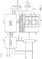
- FIG. 1 is a diagram of an integrated circuit 10 that includes memory circuitry having an arbitration circuit configured to provide synchronous and asynchronous multiport memory operation using only single-port memory elements.
- Device 10 may contain at least one memory array 14.
- memory array 14 may include memory elements (sometimes referred to as memory cells) 100 arranged in rows and columns.
- Memory cells 100 may be single-port memory cells.
- memory cell 100 may be a single-port differential memory cell having six transistors (e.g., a memory cell having a pair of access transistors that serve as a single port for the memory cell).
- Using single-port memory cells to provide dual-port memory functionality may help increase die yield, provide reduced minimum required power supply voltage (i.e., reduced power consumption), and conserve integrated circuit real estate.
- Memory array 14 may be coupled to row and column control circuitry such as row and column control circuitry 12.
- Control circuitry 12 may include row addressing circuitry, column multiplexing circuitry, write driver circuitry, read sensing circuitry, data register circuitry, etc.
- Control circuitry 12 may be used to produce desired time-varying and/or fixed signals to memory cells 100 in array 14 via paths such as paths 16 and 18.
- the signals that are supplied to memory elements 100 may sometimes be collectively referred to as control signals. In particular contexts, some of these signals may be referred to as power signals, clear signals, data signals, address signals, etc.
- a power supply signal may be distributed to all of the cells in array 14 simultaneously over a global memory power line.
- the memory power line may be oriented vertically so that there is one branch of the memory power line in each path 18 or may be oriented horizontally so that there is one branch of the memory power line in each path 16.
- a positive power supply voltage Vcc may be supplied in parallel to each cell 100 using a pattern of shared horizontal or vertical conductors.
- a ground voltage Vss may likewise be supplied in parallel to cells 100 using a pattern of shared horizontal or vertical lines.
- Control lines such as address lines and data lines are typically orthogonal to each other (e.g., address lines are horizontal while data lines are vertical or vice versa).
- Positive power supply voltage Vcc may be provided over a positive power supply line.
- Ground voltage Vss may be provided over a ground power supply line. Any suitable values may be used for positive power supply voltage Vcc and ground voltage Vss.
- positive power supply voltage Vcc may be 1.2 volts, 1.1 volts, 1.0 volts, 0.9 volts, less than 0.9 volts, or any other suitable voltage.
- Ground voltage Vss may be zero volts (as an example).
- power supply voltages Vcc may be 1.0 volts
- Vss may be zero volts
- the signal levels for address, data, and clear signals may range from zero volts (when low) to 1.0 volts (when high).
- Vcc varies as a function of time, in which Vss is less than zero volts, and in which control signals are overdriven (i.e., in which control signals have signal strengths larger than Vcc-Vss) may also be used.
- each row of array 14 may include an associated address line in a respective one of paths 16, whereas each column of array 14 may include associated data lines (e.g., true and complement data lines) in a respective one of paths 18.
- data lines e.g., true and complement data lines
- rows and columns merely represent one way of referring to particular groups of cells 100 in memory array 14 and may sometimes be used interchangeably.
- other patterns of lines may be used in paths 16 and 18. For example, different numbers of power supply signals, address signals, and data signals may be used.
- One of the address lines 16 may supply an asserted address signal to select a row of memory cells 100 to be accessed.
- the address signals on address lines 16 other than the selected address line may remain deasserted while the selected row is being accessed.
- the data lines in each column may be precharged to positive power supply voltage Vcc during read operations, whereas the data lines in each column may be driven to appropriate voltage levels to write desired write data into at least some of selected cells 100 during write operations.
- all the address signals may remain deasserted while all the data lines may be precharged to Vcc (as an example).
- the single-port memory cells 100 in array 14 may provide dual-port functionality through the use of peripheral memory circuitry.
- Row and column control circuitry 12 may receive control signals from multiplexing circuit (or multiplexer) 24.
- Multiplexing circuit 24 may have a first input configured to receive memory access requests (e.g., data and addressing signals) associated with a first memory port (port A), a second input configured to receive memory access request signals associated with a second memory port (port B), an output coupled to circuitry 12, and a control input configured to receive a port select signal PORTSEL from arbitration circuit 22 over path 26.
- Arbitration circuit 22 may be configured to receive the memory access requests from port A, the memory access requests from port B, a first clock signal Aclk that is associated with port A, and a second clock signal Bclk that is associated with port B. Arbitration circuit 22 may serve to determine the order in which to process the memory access requests received from port A and port B.
- the memory circuitry appears to function as a dual-port memory from the reference point of Aclk and Bclk, because the memory circuitry is capable of handling read and write request from at least two ports each of which is control using different clock signals Aclk and/or Bclk (e.g., arbitration circuit 22 may be capable of emulating true dual-port operation).
- Arbitration circuit 22 may drive PORTSEL low to selectively route data and addressing signals from port A to row and column control circuitry 12 using multiplexer 24 and may drive PORTSEL high to selectively route data and addressing signals from port B to row and column control circuitry 12 using multiplexer 24 (as an example).
- arbitration circuit 22 decides to execute a request, arbitration circuit 22 will temporarily assert signal START provided over path 34 to direct control circuit 20 to enable the desired read/write operation.
- control circuit 20 may provide asserted write driver enable signals to circuitry 12 during write operations and may provide asserted sense amplifier enable signals during read operations (e.g., by providing read/write enable signals from control circuit 20 to circuitry 12 over path 36) .
- read signals generated using sense amplifier circuits in circuitry 12 may be fed to output latches 28 and 30.
- Output latch 28 may be controlled using port A output clock signal Aoutclk provided over path 32 from circuit 20, whereas output latch 30 may be controlled using port B output port signal Boutclk provided over path 33 from circuit 20.
- the latched output data signals associated with the first memory port (e.g., data signal Aout) and the latched output data signals associated with the second memory port may be provided to other digital or logic circuitry on device 10 for further processing.
- arbitration circuit 22 may receive an asserted signal DONE from control circuit 20. In response to detecting an asserted DONE, arbitration circuit 22 may proceed to process a successive pending memory access request.
- Arbitration circuit 22 may be operable in a synchronous mode and an asynchronous mode. In the synchronous mode, the requests from the multiple ports may be controlled using a shared clock source. As a result, memory access requests from the multiple ports may arrive simultaneously at a rising edge of the shared clock signal. In synchronous mode, arbitration circuit 22 may, for example, determine which one of the multiple ports is to be selected.
- the port associated with the pending request may be selected for processing.
- the port that receives the read request may be selected for processing (i.e., arbitration circuit 22 may be configured to implement read port priority).
- arbitration circuit 22 may also be configured to implement write port priority (i.e., the port that receives the write request may be selected for processing).
- the second port may be given priority (i.e., the request at port B will be processed before the request at port A).
- arbitration circuitry 22 may also be configured to implement port A priority when both ports received the same type of memory requests (i.e., the request at port A will be processed before the request at port B when ports A and B both receive a read request or when ports A and B both receive a write request).
- arbitration circuit 22 may be configured to handle memory requests from any desired number of ports to support tri-port memory mode, quad-port memory mode, etc.
- arbitration circuit 22 may be configured to operate in asynchronous mode (e.g., a mode in which requests from multiple ports are controlled using clocks of different phases and/or frequencies). In asynchronous dual-port operation, requests from different memory ports often arrive at different times. As a result, arbitration circuit 22 may be configured to process a first arriving memory request as soon as it is received by circuit 22 and to process a second (later) arriving memory request when the first arrive memory request has been fulfilled.
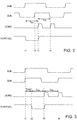
- FIGS. 2 and 3 are timing diagrams that illustrate the asynchronous mode operation of the memory circuitry of the type described in connection with FIG. 1 .
- FIG. 2 illustrates a scenario in which a port A memory access request and a port B memory access request are received at different times.
- arbitration circuit 22 may receive a first memory access request from port A (triggered by the rising clock edge of Aclk). In this example, arbitration circuit 22 is not currently handling any memory access request, so arbitration circuit 22 immediately proceeds to fulfill the first memory access request (e.g., signal PORTSEL is driven low to pass the data and addressing signals associated with the first memory access request to row and column control circuitry 12) .
- signal PORTSEL is driven low to pass the data and addressing signals associated with the first memory access request to row and column control circuitry 12
- arbitration circuit 22 may receive a second memory access request from port B (triggered by the rising clock edge of Bclk). Arbitration circuit 22 place the second memory access request on hold until it the first memory access request is fulfilled.
- signal DONE pulses high to indicate that the first memory access request has been completed.
- the amount of time it takes to perform a memory access request (e.g., the time period from the rising clock edge of Aclk to the rising edge of DONE) may sometimes be referred to as access time or clock-to-output time Tco.
- the performance of the memory circuitry may be dependent on the access time Tco for read operations if Tco associated with read operations is greater than Tco associated with write operations.
- arbitration circuit 22 may proceed to process the second memory access request by raising PORTSEL to pass the data and addressing signals associated with the second memory access request to control circuitry 12 and by directing control circuit 20 enable the desired read/write circuitry in circuitry 12.
- signal DONE pulses high to indicate that the second memory access request has been completed.
- the amount of time it takes to perform the second memory access request e.g., the time period from the previous rising edge of DONE to the current rising edge of DONE
- Tco access time
- the total latency when performing two consecutive memory access requests may therefore be equal to 2*Tco.
- FIG. 3 illustrates a scenario in which a first memory access request (e.g., a port A memory access request) and a second memory access request (e.g., a port B memory access request) are received at the same time (Aclk and Bclk clock high simultaneously).
- arbitration circuit 22 may receive a first memory access request from port A and a second memory access request form port B in parallel.
- arbitration circuit 22 may require time period Tmet to resolve metastability (i.e., to determine which one of the first and second memory access requests is to be processed first).
- arbitration circuit 22 may decide to fulfill the first memory access request by driving PORTSEL low (as an example). It is also possible that arbitration circuit 22 chooses the second memory access request for processing at time t2. At time t3, signal DONE may be pulsed high to indicate completion of the first memory access request. At this time, the second memory access request may be fulfilled (e.g., PORTSEL may be driven high). At time t4, signal DONE may again be pulsed high to indicate completion of the second memory access request.
- the total latency for performing two simultaneously arriving memory access requests (when the rising edge of Aclk and Bclk are aligned) may therefore be equal to the sum of Tmet and 2*Tco.
- FIG. 3 is merely illustrative and does not serve to limit the scope of the present invention.
- device 10 may provide multiport functionality using a semi-synchronous approach in which memory accesses are synchronized to a clock signal that is associated with a selected one of the different memory ports (sometimes referred to as the "synchronous" port).
- This clock signal may therefore be referred to herein as the synchronous port clock or the synchronous clock signal.
- Row and column control (or memory array control) circuitry 12 may be controlled using an internal memory clock signal that is synchronously related to the synchronous port clock (e.g., the internal memory clock signal may be triggered by the clock signal that is associated with the synchronous port).
- Synchronizing memory access to only one of the multiple memory ports effectively eliminates the time required for metastability resolution on the synchronous port.
- the synchronous port may be given priority so that memory access requests received at this port exhibits a minimal latency of at most one Tco.
- Memory access requests received at the other port (sometimes referred to as the "asynchronous" port) may be synchronized to the internal memory clock signal.
- Memory accesses on the asynchronous port may still incur a delay for metastability resolution, but this happens concurrently with access on the synchronous port.
- Processing memory access requests in this way may be referred to as semi-synchronous time division multiplexed (TDM) multiport memory control.
- TDM time division multiplexed
- the read port may be configured as the synchronous port while the write port is configured as the asynchronous port. If write access is given higher priority, the write port may be configured as the synchronous port while the read port is configured as the asynchronous port.
- the port associated with the more critical clock domain may be configured as the synchronous port.
- the port associated with the faster clock signal may be configured as the synchronous port (e.g., the internal memory clock may be synchronized to the second clock signal).
- the port associated with the slower clock domain may instead be configured as the synchronous port (e.g., the internal memory may also be synchronized to the first clock signal).
- the internal memory clock signal may be triggered off any one of the different port clocks.
- a memory access on the synchronous port may immediately be started.
- memory accesses from the asynchronous port may be resynchronized using the internal memory clock. Because the synchronous port access is started immediately when a memory access request is received at the synchronous port, metastability resolution of the asynchronous port occurs concurrently with access of the synchronous port, thereby reducing Tmet.
- synchronous port accesses may experience a latency of Tco
- asynchronous port accesses may experience a latency of up to one clock cycle of the synchronous port as well as other queued (or pending) accesses previously and concurrently received by the asynchronous port.
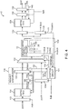
- FIG. 4 is a diagram of an exemplary implementation of a semi-synchronous dual-port memory.
- port B may be configured as the synchronous port
- port A may be configured as the asynchronous port.
- Data and address signals arriving at port A may be controlled using Aclk (referred to as the asynchronous clock), whereas data and address signals arriving at port B may be controlled using Bclk (referred to as the synchronous clock).
- Signals Aclk and Bclk may have different clock frequencies/phases.
- the signals from the synchronous port may be received using latch 104.
- Latch 104 may have a clock control input configured to received Bclk and an output that is coupled to a first input of multiplexing circuit 102.
- Synchronous clock Bclk may be fed to control circuit 101.
- Control circuit 101 may be used to generate internal memory clock signals and may serve as a sequencing circuit operable to determine the order in which to fulfill incoming memory access requests.
- control circuit may be used to generate internal memory clock Mclk over path 108, port A synchronizing clock Arclk over path 124, port A output clock Aoutclk over path 109, port B output control clock Boutclk over pat 111, and multiplexer control signal PORTSEL over path 113.
- the signals from the asynchronous port may be received using latch 112.
- Latch 112 may have a clock control input configured to receive Aclk and an output that is coupled to an asynchronous first-in-first-out (FIFO) circuit 114.
- FIFO 114 may sometimes be referred to as a buffer circuit.
- Asynchronous FIFO 114 may be used to buffer incoming requests on port A while requests from port B are being processed.
- FIFO 114 may have outputs coupled to a metastability synchronizer such as request synchronizer 116.
- FIFO 114 may have a first output at which data and address signals associated with a current pending request are provided and a second output at which signal Aasync is provided.
- Request synchronizer 116 may include a positive-edge-triggered latch 118 and a negative edge triggered latch 120.
- Positive-edge-triggered latch 118 may have an input that receives signal Aasync from the second output of FIFO 114, a control input coupled to path 124, and an output at which signal Areq is provided.
- Negative-edge-triggered latch 120 may have a first input that receives the data and address signals associated with the current pending request from the first output of FIFO 114, a second input that receives signal Areq from the output of latch 118, a control input coupled to path 124, a first output that is coupled to a second input of multiplexer 102, and second output at which signal Areqsyn is provided.
- Signal Areqsyn may be fed to control circuit 101 over path 122.
- Multiplexer 102 may be controlled using signal PORTSEL generated from control circuit 101 to selectively route memory access request signals from one of ports A and B to its output.
- Memory row and column control circuitry (sometimes referred to as memory array control circuitry) 12 may receive data and addressing signals from the output of multiplexer 102. Circuitry 12 may be controlled using internal memory clock Mclk conveyed over path 108 from control circuit 101. Circuitry 12 may also generate a signal DONE to control circuit 101 over path 110 to indicate completion of a memory access request that has currently been serviced. Signal Arclk generated using control circuit 101 may be fed to the control input of latches 118 and 120 over path 124. FIFO 114 may also be configured to receive signal Areq fed back from the output of latch 118 and signal Arclk.
- Port A output latch 132 may be controlled using Aoutclk, whereas port B output latch 130 may be controlled using Boutclk. Signals Aoutclk and Boutclk may be generated using control circuit 101.
- Port B output latch 130 may have an output at which port B output signal Bout is provided.
- Port A output latch 132 may have an output coupled to output asynchronous FIFO 134. Similar to input FIFO 114, output asynchronous FIFO 134 may serve to buffer the port A output data signals.
- the port A output data signals may then be passed through positive-edge-triggered latch 136 and negative-edge-triggered latch 138.
- FIFO 134 and latches 136 and 138 may be clocked using signal Aclk.
- Latch 138 may have a first output at which port A output signal Aout is provided and a second output at which port A output acknowledge signal Ack is provided.
- Signal Ack may be fed back to asynchronous FIFO 134 over path 140.
- An asserted Ack received at FIFO 134 may indicate that a word of data has been successfully latched at the output and may direct FIFO 134 to shift its contents.
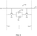
- FIG. 5 is a circuit diagram of an exemplary single-port memory cell 100 that may be formed in memory array 14.
- cell 100 may include at least one pair of cross-coupled inverters 142 and 144 each having an input and an output.
- the input of inverter 142 may be coupled to the output of inverter 144, whereas the input of inverter 144 may be coupled to the output of inverter 142.
- the output of inverter 144 may serve as a first internal data storage node for cell 100, whereas the output of inverter 142 may serve as a second internal data storage node for cell 100.
- Inverters 142 and 144 cross-coupled in this way may serve to store a single bit of data (e.g., a true version of the data bit may be stored on the first data storage node, whereas an inverted version of the data bit may be stored on the second data storage node) and may sometimes be referred to as a bistable element.
- a first access transistor 146 may be coupled between the first data storage node and a first data line 18-1.
- a second access transistor 148 may be coupled between the second data storage node and a second data line 18-2.
- Data lines 18-1 and 18-2 may sometimes be referred to as a true and complement bit line pair.
- Data lines 18-1 and 18-2 may be driven to appropriate values to write data into cell 100 during write operations and may be precharged to a power supply voltage level during read operations.
- Access transistors 146 and 148 may be controlled by word line signal WL provided over word line 16.
- Signal WL may be asserted to select a row of memory cells 100 in array 14 to be accessed.
- Signal WL in the remaining unselected rows may remain deasserted.
- the single-port memory cell of FIG. 5 is merely illustrative and is not intended to limit the scope of the present invention. If desired, memory cell 100 may include more than two cross-coupled inverting circuits, may include a read buffer circuit, may have a single-ended architecture, etc.
- TDM memory circuitry described in connection with FIG. 4 may be as follows.
- a series of memory access requests may be triggered in response to detecting a rising clock edge in the synchronous port clock (i.e., port B).
- Internal memory clock Mclk may be triggered to assert on a rising edge of synchronous clock Bclk and may be triggered to negate (i.e., deassert) on a rising edge of DONE. If desired, Mclk may be triggered to negate on the falling edge of DONE.
- a port B access In response to detecting a rising Mclk edge, a port B access is immediately performed so that port B access time is as fast as true dual-port memory (i.e., dual-port memory implemented using dual-port memory cells having eight memory cell transistors).
- DONE When DONE is asserted, Boutclk may be pulsed high to latch output data signal Bout.
- port A input asynchronous FIFO 114 may be used to buffer incoming port A memory access requests.
- Signal Arclk may be used to synchronize port A memory access requests.
- a rising Bclk edge may trigger signal Arclk to be pulsed high for a predetermined time period.
- Signal Aasync may generally be asserted if FIFO 114 contains at least one pending port A request.
- Aasync will be sampled during the first half cycle of Arclk to produce Areq using latch 118 (e.g., Aasync will be sampled on a positive clock edge of Arclk), whereas Areq will be sampled during a second half cycle of Arclk to produce Areqsyn using latch 120 (e.g., Areqsyn will be sampled on a negative clock edge of Arclk).
- Synchronized port A request signal Areqsyn may then be fed to control circuit 101 to indicate that a port A request has yet to be fulfilled during the current Bclk cycle. Sampling and re-sampling a pending port A request in this way may serve to synchronize the port A request to internal memory clock Mclk.
- Signal Areq and Arclk may be fed back to asynchronous FIFO 114 as a form of acknowledgement.
- Aasync may be negated to indicate that a pending request has been sampled (e.g., to delete that pending request from FIFO 114).
- Asynchronous FIFO 114 may subsequently shift its contents and if FIFO 114 contains additional pending requests that need to be service, Aasync will be asserted asynchronously.
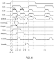
- FIG. 6 is a timing diagram illustrating the operation of the semi-synchronous TDM memory circuitry when the synchronous port clock is faster than the asynchronous port clock (e.g., when Bclk has a frequency that is greater than the frequency of Aclk).
- asynchronous FIFO 114 contains no pending request prior to time t1.
- Signal PORTSEL may be high by default to select a port B request for processing.
- signal Aclk may clock high and a port A request may enter FIFO 114.
- This addition of a new port A request may cause signal Aasync to be asynchronously asserted some time after t1 (e.g., at time t2).
- signal Bclk may clock high and a B port request may be presented at the output of latch 104 (see, e.g., FIG. 4 ).
- This rising edge of Bclk may trigger Mclk to be asserted and may trigger Arclk to be pulsed high for a predetermined pulse width of PW.
- the rising clock edge of Arclk may cause latch 118 to sample Aasync so that Areq will have the same value as Aasync (e.g., the rising edge of Arclk causes Areq to rise high because Aasync is high at time t3).
- Arclk may be deasserted.
- a falling clock edge of Arclk may cause Aasync to be negated (only if Areq is high) and may cause latch 120 to sample Areq so that Areqsyn will have the same value as Areq.
- the port A request that arrived at time t1 may be deleted from FIFO 114 since it has already been latched by request synchronizer 116.
- the falling edge of Arclk will cause Areqsyn to rise high because Areq is high at time t4.
- Signal Aasync may remain negated since there are no additional memory access requests from port A.
- the port B memory access request is fulfilled and signal DONE is pulsed high, thereby causing Mclk to be deasserted and Boutclk to be pulsed high.
- Signal Boutclk may only be pulsed high in response to completion of a port B memory access.
- the time from the start of the port B memory access request to corresponding signal DONE being asserted may be equal to access time Tco. Since there is a pending port A memory request (as indicated by an asserted Areqsyn), control circuit 101 may temporarily invert PORTSEL so that the port A memory request may be serviced.
- DONE may be deasserted.
- a subsequent port A memory access may be serviced.
- Mclk may be raised high and Arclk may be pulsed high to signify the start of the port A memory access.
- Areq may fall low because there are no newly arriving port A requests (as indicated by a low Aasync).
- Arclk may be deasserted.
- a falling clock edge of Arclk may sample Areq, thereby causing Areqsyn to fall low because Areq is low at time t7.
- a low Areqsyn may indicate that there are no pending port A memory access requests.
- signal DONE is pulsed high and causes Mclk to be deasserted and Aoutclk to be pulsed high.
- Signal Aoutclk may only be pulsed high in response to completion of a port A memory access.
- Bclk may clock high, and a second port B memory access request may be serviced.
- Bclk may clock high, and a third port B memory access request may be serviced.
- the latency of the port A access is increased only by at most one port B cycle, which may be acceptable in true dual-port emulation.
- Bclk is much faster than Aclk (e.g., when Bclk is at least three times, at least five times, or at least ten times faster than Aclk)
- the port A access may be guaranteed to be completed within a small fraction of Aclk.
- FIG. 7 is a timing diagram illustrating the operation of the semi-synchronous TDM memory circuitry when the asynchronous port clock is faster than the synchronous port clock (e.g., when Bclk has a frequency that is less than the frequency of Aclk).
- the example of FIG. 7 assumes that asynchronous FIFO 114 contains at least one pending request prior to time t1 (as indicated by asserted Aasync before time t1).
- Signal PORTSEL may be high by default to select port B request for processing.
- signals Aclk and Bclk may clock high simultaneously (e.g., a new port A memory access request and a new port B memory access request may arrive in parallel).
- a rising Bclk will trigger Arclk and Mclk to clock high and Areq to rise (because Aasync is high at time t1).
- the synchronous port access i.e., the port B memory access
- Arclk may clock low, causing Aasync to negate (e.g., the pending memory access request that was stored in FIFO 114 prior to time t1 may be deleted from FIFO 114 since it has already been latched by request synchronizer 116) and Areqsyn to rise high (because Areq is high at time t2).
- signal DONE may be temporarily asserted to indicate completion of the port B memory access, thereby triggering Mclk to clock low.
- PORTSEL may be driven low to select port A for servicing, because there is at least one pending port A request that needs to be serviced (i.e., an unserviced port A request that is currently stored in synchronizer 116), as indicated by a high Areqsyn.
- signal Aasync may be asserted since there FIFO 114 still contains a queued port B memory access that arrived at time t1.
- control circuit 101 may drive Arclk and Mclk high.
- Signal Aasync may be sampled using latch 118 but Areq will remain high since Aasync is high at time t4.
- Arclk may clock low, causing Aasync to negate (e.g., the pending memory access request that arrived at time t1 may be deleted since it has just been latched by request synchronizer 116).
- Signal Areq may be sampled using latch 120 but Areqsyn will remain high since Areq is high at time t5.
- signal DONE may be temporarily asserted to indicate completion of the queued port A memory access, thereby triggering Mclk to clock low.
- Signal PORTSEL may remain low since there is still a port A memory access request that has yet to be serviced.
- Aclk may clock high and a first additional port A memory access request may enter FIFO 114.
- signal Aasync may be asserted since FIFO 114 still contains the first additional port A memory access request that arrived at time t6.
- control circuit 101 may drive Arclk and Mclk high.
- Signal Aasync may be sampled using latch 118, and Areq will remain high since Aasync is high at time t7.
- Arclk may clock low, causing Aasync to negate (e.g., the first additional port A memory access request that arrived at time t6 may be deleted).
- Signal Areq may be sampled using latch 220 but Areqsyn will remain high since Areq is high at time t8.
- signal DONE may be temporarily asserted to indicate completion of the current port A memory access, thereby triggering Mclk to clock low.
- Signal PORTSEL may remain low since there is still the first additional port A memory access request that has yet to be serviced.
- Signal Aasync may remain negated since there are no additional queued requests in FIFO 114 at this time.
- DONE may be deasserted and the first additional port A memory access request that arrived at time t6 may be serviced.
- control circuit 101 may drive Arclk and Mclk high.
- Signal Aasync may be sampled using latch 118, causing Areq to fall low since Aasync is low at time t10.
- Aclk may clock high and a second additional port A memory access request may enter FIFO 114, causing Aasync to rise high.
- Arclk may clock low.
- FIFO 114 may only be configured to delete a request at the falling clock edge of Arclk if and only if Areq is high.
- Signal Areq may be sampled using latch 120, causing Areqsyn to fall low since Areq is low at time t12.
- signal DONE may be temporarily asserted to indicate completion of the first additional port A memory access, thereby triggering Mclk to clock low.
- Signal PORTSEL may be driven back high if Areq is low.
- Signal Aasync will remain high since no additional port A requests will be serviced for the remainder of the current Bclk cycle.
- a new port A memory request may arrive and may be stored in FIFO 114 for at least until the rising edge of Bclk.
- the depth of FIFO 114 may be configured to be sufficiently deep to accommodate the number of port A requests that can occur in a port B clock cycle. If desired, the asynchronous arbitration multiport emulation approach described in connection with FIG. 1 may be used when Aclk is faster than Bclk.
- FIG. 8 is a flow chart of illustrative steps involved in fulfilling memory access requests using the semi-synchronous TDM multiport memory circuitry of the type shown in FIG. 4 .
- control circuit 101 may wait for a Bclk rising edge.
- Signal PORTSEL may be set to its default value of one (i.e., to selective route a synchronous port B request to memory array control circuitry 12). If input FIFO 114 is not empty, signal Aasync may be asynchronously set to one (step 302).
- control circuit 101 may raise internal memory clock Mclk and pulse Arclk high (step 304).
- Aasync may be sampled using latch 118 (e.g., Areq is set to the sampled value of Aasync). If there is a port B memory access request that has yet to be serviced, processing may proceed to step 310. If no port B request is present, processing may proceed to step 318 after Arclk is negated.
- the desired port B read/write memory access may be performed.
- Areq may be sampled using latch 120 (e.g., Areqsyn is set to the sampled valued of Areq), as shown in step 312. If Areq is high, the output of FIFO 114 is latched, thereby causing Aasync to be negated and the oldest port A memory access request (i.e., a port A memory access request arriving before any other request currently stored in FIFO 114) may be deleted from FIFO 114.
- DONE may be pulsed high, thereby triggering Mclk to clock low and Boutclk to pulse high.
- Aasync may be asserted if FIFO 114 contains at least one unserviced request. Processing may then proceed to step 318, as indicated by path 317.
- control circuit 101 may check whether Areqsyn is high or low. If Areqsyn is low, processing may loop back to step 300 as indicated by path 320 (e.g., control circuit 101 will defer any port A requests for the remainder of the current Bclk cycle). If Areqsyn is high, processing may proceed to step 320.
- signal PORTSEL may be set to zero (i.e., to selective route an asynchronous port A request to memory array control circuitry 12).
- signal Mclk may be clocked high and Arclk may be pulsed high (step 322).
- Aasync may be sampled using latch 118 (e.g., Areq is set to the sampled value of Aasync).
- the desired port A read/write memory access may be performed.
- Areq may be sampled using latch 120 (e.g., Areqsyn is set to the sampled valued of Areq), as shown in step 328.
- Aasync may be negated (e.g., the oldest port A memory access request presently stored in FIFO 114 may be removed).
- DONE may be pulsed high, thereby triggering Mclk to clock low and Aoutclk to pulse high. Processing may loop back to step 316 to process an additional A port request, if present, as indicated by path 332.
- the dual-port implementations of the memory circuitry with arbitration circuit 22 of FIG. 1 and the memory circuitry with semi-synchronous TDM sequencing circuit 101 of FIG. 4 are merely illustrative and do not serve to limit the scope of the present invention. If desired, the asynchronous and semi-synchronous dual-port emulation techniques described herein may be applied to emulate tri-port memory operation, quad-port memory operation, etc.
Landscapes
- Engineering & Computer Science (AREA)
- Theoretical Computer Science (AREA)
- Physics & Mathematics (AREA)
- General Engineering & Computer Science (AREA)
- General Physics & Mathematics (AREA)
- Multimedia (AREA)
- Static Random-Access Memory (AREA)
- Memory System (AREA)
Applications Claiming Priority (1)
| Application Number | Priority Date | Filing Date | Title |
|---|---|---|---|
| US13/284,721 US8806259B2 (en) | 2011-10-28 | 2011-10-28 | Time division multiplexed multiport memory implemented using single-port memory elements |
Publications (3)
| Publication Number | Publication Date |
|---|---|
| EP2587486A2 EP2587486A2 (en) | 2013-05-01 |
| EP2587486A3 EP2587486A3 (en) | 2013-06-12 |
| EP2587486B1 true EP2587486B1 (en) | 2019-09-11 |
Family
ID=47225945
Family Applications (1)
| Application Number | Title | Priority Date | Filing Date |
|---|---|---|---|
| EP12189371.3A Active EP2587486B1 (en) | 2011-10-28 | 2012-10-22 | Time division multiplexed multiport memory |
Country Status (4)
| Country | Link |
|---|---|
| US (2) | US8806259B2 (enExample) |
| EP (1) | EP2587486B1 (enExample) |
| JP (2) | JP6088200B2 (enExample) |
| CN (1) | CN103093808B (enExample) |
Families Citing this family (9)
| Publication number | Priority date | Publication date | Assignee | Title |
|---|---|---|---|---|
| US9230622B2 (en) * | 2012-11-30 | 2016-01-05 | Taiwan Semiconductor Manufacturing Company, Ltd. | Simultaneous two/dual port access on 6T SRAM |
| US10289186B1 (en) * | 2013-10-31 | 2019-05-14 | Maxim Integrated Products, Inc. | Systems and methods to improve energy efficiency using adaptive mode switching |
| CN104318952B (zh) * | 2014-09-30 | 2017-11-10 | 西安紫光国芯半导体有限公司 | Dram中一种减少电压端口的电路及方法 |
| US10430215B1 (en) * | 2015-06-25 | 2019-10-01 | Cadence Design Systems, Inc. | Method and system to transfer data between hardware emulator and host workstation |
| JP6637872B2 (ja) * | 2016-10-28 | 2020-01-29 | ルネサスエレクトロニクス株式会社 | マルチポートメモリおよび半導体装置 |
| US10652912B2 (en) | 2018-04-30 | 2020-05-12 | Microchip Technology Incorporated | Smart radio arbiter with conflict resolution based on timing predictability |
| US11194942B1 (en) * | 2018-12-06 | 2021-12-07 | Cadence Design Systems, Inc. | Emulation system supporting four-state for sequential logic circuits |
| CN110059036B (zh) * | 2019-04-15 | 2022-04-26 | 西安微电子技术研究所 | 一种存储体内部多异步接口访问控制装置及方法 |
| KR102767986B1 (ko) * | 2020-02-17 | 2025-02-14 | 에스케이하이닉스 주식회사 | 반도체장치 |
Citations (1)
| Publication number | Priority date | Publication date | Assignee | Title |
|---|---|---|---|---|
| US20070091708A1 (en) * | 2005-10-17 | 2007-04-26 | Oki Electric Industry Co., Ltd. | Semiconductor storage device |
Family Cites Families (24)
| Publication number | Priority date | Publication date | Assignee | Title |
|---|---|---|---|---|
| JPS63285648A (ja) * | 1987-05-19 | 1988-11-22 | Fujitsu Ltd | メモリアクセス調停方式 |
| US4796232A (en) | 1987-10-20 | 1989-01-03 | Contel Corporation | Dual port memory controller |
| US4937781A (en) | 1988-05-13 | 1990-06-26 | Dallas Semiconductor Corporation | Dual port ram with arbitration status register |
| US5047921A (en) | 1989-01-31 | 1991-09-10 | International Business Machines Corporation | Asynchronous microprocessor random access memory arbitration controller |
| US5708850A (en) * | 1994-07-27 | 1998-01-13 | Sony Corporation | Parallel processing system for time division multiplex data transfer including read/write dual port memory accessible to bus and digital signal processor during opposite phases of clock |
| JPH0944395A (ja) * | 1995-08-02 | 1997-02-14 | Fujitsu Ltd | 非同期アクセス調停方式 |
| US5768211A (en) | 1996-07-31 | 1998-06-16 | Cypress Semiconductor Corporation | Multi-port arbitration for high performance width expansion |
| TW451215B (en) * | 1998-06-23 | 2001-08-21 | Motorola Inc | Pipelined dual port integrated circuit memory |
| US5973985A (en) | 1998-08-11 | 1999-10-26 | Stmicroelectronics, Inc. | Dual port SRAM cell having pseudo ground line or pseudo power line |
| US6388939B1 (en) | 1999-09-30 | 2002-05-14 | Cypress Semiconductor Corp. | Dual port sram |
| US6118689A (en) | 1999-10-27 | 2000-09-12 | Kuo; James B. | Two-port 6T CMOS SRAM cell structure for low-voltage VLSI SRAM with single-bit-line simultaneous read-and-write access (SBLSRWA) capability |
| US6816955B1 (en) | 2000-09-29 | 2004-11-09 | Cypress Semiconductor Corp. | Logic for providing arbitration for synchronous dual-port memory |
| US6751151B2 (en) | 2001-04-05 | 2004-06-15 | International Business Machines Corporation | Ultra high-speed DDP-SRAM cache |
| US6606275B2 (en) | 2001-08-23 | 2003-08-12 | Jeng-Jye Shau | High performance semiconductor memory devices |
| US7421559B1 (en) * | 2003-12-18 | 2008-09-02 | Cypress Semiconductor Corporation | Apparatus and method for a synchronous multi-port memory |
| KR100560948B1 (ko) | 2004-03-31 | 2006-03-14 | 매그나칩 반도체 유한회사 | 6 트랜지스터 듀얼 포트 에스램 셀 |
| JP2006252656A (ja) * | 2005-03-10 | 2006-09-21 | Nec Electronics Corp | マルチポートメモリ装置 |
| JP4914034B2 (ja) | 2005-06-28 | 2012-04-11 | セイコーエプソン株式会社 | 半導体集積回路 |
| US7603496B2 (en) * | 2006-01-23 | 2009-10-13 | Arm Limited | Buffering data during data transfer through a plurality of channels |
| JP5038657B2 (ja) * | 2006-06-26 | 2012-10-03 | ルネサスエレクトロニクス株式会社 | 半導体集積回路装置 |
| US7564738B2 (en) | 2006-08-11 | 2009-07-21 | Freescale Semiconductor, Inc. | Double-rate memory |
| KR100846386B1 (ko) * | 2006-09-21 | 2008-07-15 | 주식회사 하이닉스반도체 | 멀티포트 메모리 장치 |
| JP2009238351A (ja) * | 2008-03-28 | 2009-10-15 | Oki Semiconductor Co Ltd | デュアルポート半導体記憶装置およびそのタイミング発生装置 |
| JP2010044821A (ja) * | 2008-08-11 | 2010-02-25 | Hitachi Ulsi Systems Co Ltd | 半導体装置とメモリマクロ |
-
2011
- 2011-10-28 US US13/284,721 patent/US8806259B2/en active Active
-
2012
- 2012-10-22 JP JP2012232813A patent/JP6088200B2/ja not_active Expired - Fee Related
- 2012-10-22 EP EP12189371.3A patent/EP2587486B1/en active Active
- 2012-10-29 CN CN201210421421.2A patent/CN103093808B/zh active Active
-
2014
- 2014-07-15 US US14/332,006 patent/US9298211B2/en active Active
-
2017
- 2017-02-03 JP JP2017018597A patent/JP6293322B2/ja active Active
Patent Citations (1)
| Publication number | Priority date | Publication date | Assignee | Title |
|---|---|---|---|---|
| US20070091708A1 (en) * | 2005-10-17 | 2007-04-26 | Oki Electric Industry Co., Ltd. | Semiconductor storage device |
Also Published As
| Publication number | Publication date |
|---|---|
| JP6088200B2 (ja) | 2017-03-01 |
| JP2017091577A (ja) | 2017-05-25 |
| JP6293322B2 (ja) | 2018-03-14 |
| US20130111253A1 (en) | 2013-05-02 |
| CN103093808B (zh) | 2017-03-01 |
| US9298211B2 (en) | 2016-03-29 |
| US8806259B2 (en) | 2014-08-12 |
| US20140331074A1 (en) | 2014-11-06 |
| JP2013097792A (ja) | 2013-05-20 |
| EP2587486A2 (en) | 2013-05-01 |
| EP2587486A3 (en) | 2013-06-12 |
| CN103093808A (zh) | 2013-05-08 |
Similar Documents
| Publication | Publication Date | Title |
|---|---|---|
| EP2587486B1 (en) | Time division multiplexed multiport memory | |
| US8867303B2 (en) | Memory arbitration circuitry | |
| JP5260511B2 (ja) | シングルポートメモリセルを用いたデュアルポートsramメモリ | |
| US20010026497A1 (en) | Method and system for accessing rows in multiple memory banks within an integrated circuit | |
| EP2808801B1 (en) | Multiple data rate memory with read timing information | |
| JP2007525766A (ja) | マルチポートメモリシステムにおける衝突検出 | |
| CN100547681C (zh) | 存储器装置及在存储器装置中读取数据的方法 | |
| US20060171239A1 (en) | Dual Port Memory Unit Using a Single Port Memory Core | |
| US6259648B1 (en) | Methods and apparatus for implementing pseudo dual port memory | |
| US8462568B2 (en) | Command latency systems and methods | |
| JP2005071454A (ja) | 半導体記憶装置 | |
| US7405995B2 (en) | Semiconductor storage device | |
| JP5038657B2 (ja) | 半導体集積回路装置 | |
| KR0154741B1 (ko) | 듀얼포트 메모리 장치 및 듀얼포트 메모리 장치의 시리얼데이타 출력방법 | |
| US9501407B1 (en) | First-in-first-out memory with dual memory banks | |
| CN104376870B (zh) | 预测及避免亚稳态的存储器仲裁电路系统及其方法 | |
| JP2009087534A (ja) | 半導体記憶装置 | |
| CN116230047A (zh) | 虚拟静态随机存取存储器 | |
| JPH05151077A (ja) | 情報処理装置 |
Legal Events
| Date | Code | Title | Description |
|---|---|---|---|
| PUAI | Public reference made under article 153(3) epc to a published international application that has entered the european phase |
Free format text: ORIGINAL CODE: 0009012 |
|
| AK | Designated contracting states |
Kind code of ref document: A2 Designated state(s): AL AT BE BG CH CY CZ DE DK EE ES FI FR GB GR HR HU IE IS IT LI LT LU LV MC MK MT NL NO PL PT RO RS SE SI SK SM TR |
|
| AX | Request for extension of the european patent |
Extension state: BA ME |
|
| PUAL | Search report despatched |
Free format text: ORIGINAL CODE: 0009013 |
|
| AK | Designated contracting states |
Kind code of ref document: A3 Designated state(s): AL AT BE BG CH CY CZ DE DK EE ES FI FR GB GR HR HU IE IS IT LI LT LU LV MC MK MT NL NO PL PT RO RS SE SI SK SM TR |
|
| AX | Request for extension of the european patent |
Extension state: BA ME |
|
| RIC1 | Information provided on ipc code assigned before grant |
Ipc: G11C 7/10 20060101AFI20130506BHEP |
|
| 17P | Request for examination filed |
Effective date: 20131212 |
|
| RBV | Designated contracting states (corrected) |
Designated state(s): AL AT BE BG CH CY CZ DE DK EE ES FI FR GB GR HR HU IE IS IT LI LT LU LV MC MK MT NL NO PL PT RO RS SE SI SK SM TR |
|
| STAA | Information on the status of an ep patent application or granted ep patent |
Free format text: STATUS: EXAMINATION IS IN PROGRESS |
|
| 17Q | First examination report despatched |
Effective date: 20171129 |
|
| GRAP | Despatch of communication of intention to grant a patent |
Free format text: ORIGINAL CODE: EPIDOSNIGR1 |
|
| STAA | Information on the status of an ep patent application or granted ep patent |
Free format text: STATUS: GRANT OF PATENT IS INTENDED |
|
| INTG | Intention to grant announced |
Effective date: 20190430 |
|
| GRAS | Grant fee paid |
Free format text: ORIGINAL CODE: EPIDOSNIGR3 |
|
| GRAA | (expected) grant |
Free format text: ORIGINAL CODE: 0009210 |
|
| STAA | Information on the status of an ep patent application or granted ep patent |
Free format text: STATUS: THE PATENT HAS BEEN GRANTED |
|
| AK | Designated contracting states |
Kind code of ref document: B1 Designated state(s): AL AT BE BG CH CY CZ DE DK EE ES FI FR GB GR HR HU IE IS IT LI LT LU LV MC MK MT NL NO PL PT RO RS SE SI SK SM TR |
|
| REG | Reference to a national code |
Ref country code: GB Ref legal event code: FG4D |
|
| REG | Reference to a national code |
Ref country code: CH Ref legal event code: EP |
|
| REG | Reference to a national code |
Ref country code: AT Ref legal event code: REF Ref document number: 1179516 Country of ref document: AT Kind code of ref document: T Effective date: 20190915 |
|
| REG | Reference to a national code |
Ref country code: IE Ref legal event code: FG4D |
|
| REG | Reference to a national code |
Ref country code: DE Ref legal event code: R096 Ref document number: 602012063836 Country of ref document: DE |
|
| REG | Reference to a national code |
Ref country code: NL Ref legal event code: MP Effective date: 20190911 |
|
| REG | Reference to a national code |
Ref country code: LT Ref legal event code: MG4D |
|
| PG25 | Lapsed in a contracting state [announced via postgrant information from national office to epo] |
Ref country code: SE Free format text: LAPSE BECAUSE OF FAILURE TO SUBMIT A TRANSLATION OF THE DESCRIPTION OR TO PAY THE FEE WITHIN THE PRESCRIBED TIME-LIMIT Effective date: 20190911 Ref country code: BG Free format text: LAPSE BECAUSE OF FAILURE TO SUBMIT A TRANSLATION OF THE DESCRIPTION OR TO PAY THE FEE WITHIN THE PRESCRIBED TIME-LIMIT Effective date: 20191211 Ref country code: HR Free format text: LAPSE BECAUSE OF FAILURE TO SUBMIT A TRANSLATION OF THE DESCRIPTION OR TO PAY THE FEE WITHIN THE PRESCRIBED TIME-LIMIT Effective date: 20190911 Ref country code: LT Free format text: LAPSE BECAUSE OF FAILURE TO SUBMIT A TRANSLATION OF THE DESCRIPTION OR TO PAY THE FEE WITHIN THE PRESCRIBED TIME-LIMIT Effective date: 20190911 Ref country code: NO Free format text: LAPSE BECAUSE OF FAILURE TO SUBMIT A TRANSLATION OF THE DESCRIPTION OR TO PAY THE FEE WITHIN THE PRESCRIBED TIME-LIMIT Effective date: 20191211 Ref country code: FI Free format text: LAPSE BECAUSE OF FAILURE TO SUBMIT A TRANSLATION OF THE DESCRIPTION OR TO PAY THE FEE WITHIN THE PRESCRIBED TIME-LIMIT Effective date: 20190911 |
|
| PG25 | Lapsed in a contracting state [announced via postgrant information from national office to epo] |
Ref country code: LV Free format text: LAPSE BECAUSE OF FAILURE TO SUBMIT A TRANSLATION OF THE DESCRIPTION OR TO PAY THE FEE WITHIN THE PRESCRIBED TIME-LIMIT Effective date: 20190911 Ref country code: GR Free format text: LAPSE BECAUSE OF FAILURE TO SUBMIT A TRANSLATION OF THE DESCRIPTION OR TO PAY THE FEE WITHIN THE PRESCRIBED TIME-LIMIT Effective date: 20191212 Ref country code: ES Free format text: LAPSE BECAUSE OF FAILURE TO SUBMIT A TRANSLATION OF THE DESCRIPTION OR TO PAY THE FEE WITHIN THE PRESCRIBED TIME-LIMIT Effective date: 20190911 Ref country code: AL Free format text: LAPSE BECAUSE OF FAILURE TO SUBMIT A TRANSLATION OF THE DESCRIPTION OR TO PAY THE FEE WITHIN THE PRESCRIBED TIME-LIMIT Effective date: 20190911 Ref country code: RS Free format text: LAPSE BECAUSE OF FAILURE TO SUBMIT A TRANSLATION OF THE DESCRIPTION OR TO PAY THE FEE WITHIN THE PRESCRIBED TIME-LIMIT Effective date: 20190911 |
|
| REG | Reference to a national code |
Ref country code: AT Ref legal event code: MK05 Ref document number: 1179516 Country of ref document: AT Kind code of ref document: T Effective date: 20190911 |
|
| PG25 | Lapsed in a contracting state [announced via postgrant information from national office to epo] |
Ref country code: AT Free format text: LAPSE BECAUSE OF FAILURE TO SUBMIT A TRANSLATION OF THE DESCRIPTION OR TO PAY THE FEE WITHIN THE PRESCRIBED TIME-LIMIT Effective date: 20190911 Ref country code: NL Free format text: LAPSE BECAUSE OF FAILURE TO SUBMIT A TRANSLATION OF THE DESCRIPTION OR TO PAY THE FEE WITHIN THE PRESCRIBED TIME-LIMIT Effective date: 20190911 Ref country code: PL Free format text: LAPSE BECAUSE OF FAILURE TO SUBMIT A TRANSLATION OF THE DESCRIPTION OR TO PAY THE FEE WITHIN THE PRESCRIBED TIME-LIMIT Effective date: 20190911 Ref country code: RO Free format text: LAPSE BECAUSE OF FAILURE TO SUBMIT A TRANSLATION OF THE DESCRIPTION OR TO PAY THE FEE WITHIN THE PRESCRIBED TIME-LIMIT Effective date: 20190911 Ref country code: PT Free format text: LAPSE BECAUSE OF FAILURE TO SUBMIT A TRANSLATION OF THE DESCRIPTION OR TO PAY THE FEE WITHIN THE PRESCRIBED TIME-LIMIT Effective date: 20200113 Ref country code: EE Free format text: LAPSE BECAUSE OF FAILURE TO SUBMIT A TRANSLATION OF THE DESCRIPTION OR TO PAY THE FEE WITHIN THE PRESCRIBED TIME-LIMIT Effective date: 20190911 Ref country code: IT Free format text: LAPSE BECAUSE OF FAILURE TO SUBMIT A TRANSLATION OF THE DESCRIPTION OR TO PAY THE FEE WITHIN THE PRESCRIBED TIME-LIMIT Effective date: 20190911 |
|
| PG25 | Lapsed in a contracting state [announced via postgrant information from national office to epo] |
Ref country code: SM Free format text: LAPSE BECAUSE OF FAILURE TO SUBMIT A TRANSLATION OF THE DESCRIPTION OR TO PAY THE FEE WITHIN THE PRESCRIBED TIME-LIMIT Effective date: 20190911 Ref country code: SK Free format text: LAPSE BECAUSE OF FAILURE TO SUBMIT A TRANSLATION OF THE DESCRIPTION OR TO PAY THE FEE WITHIN THE PRESCRIBED TIME-LIMIT Effective date: 20190911 Ref country code: CZ Free format text: LAPSE BECAUSE OF FAILURE TO SUBMIT A TRANSLATION OF THE DESCRIPTION OR TO PAY THE FEE WITHIN THE PRESCRIBED TIME-LIMIT Effective date: 20190911 Ref country code: IS Free format text: LAPSE BECAUSE OF FAILURE TO SUBMIT A TRANSLATION OF THE DESCRIPTION OR TO PAY THE FEE WITHIN THE PRESCRIBED TIME-LIMIT Effective date: 20200224 |
|
| REG | Reference to a national code |
Ref country code: CH Ref legal event code: PL |
|
| REG | Reference to a national code |
Ref country code: DE Ref legal event code: R097 Ref document number: 602012063836 Country of ref document: DE |
|
| PLBE | No opposition filed within time limit |
Free format text: ORIGINAL CODE: 0009261 |
|
| STAA | Information on the status of an ep patent application or granted ep patent |
Free format text: STATUS: NO OPPOSITION FILED WITHIN TIME LIMIT |
|
| PG2D | Information on lapse in contracting state deleted |
Ref country code: IS |
|
| PG25 | Lapsed in a contracting state [announced via postgrant information from national office to epo] |
Ref country code: CH Free format text: LAPSE BECAUSE OF NON-PAYMENT OF DUE FEES Effective date: 20191031 Ref country code: LU Free format text: LAPSE BECAUSE OF NON-PAYMENT OF DUE FEES Effective date: 20191022 Ref country code: LI Free format text: LAPSE BECAUSE OF NON-PAYMENT OF DUE FEES Effective date: 20191031 Ref country code: DK Free format text: LAPSE BECAUSE OF FAILURE TO SUBMIT A TRANSLATION OF THE DESCRIPTION OR TO PAY THE FEE WITHIN THE PRESCRIBED TIME-LIMIT Effective date: 20190911 Ref country code: IS Free format text: LAPSE BECAUSE OF FAILURE TO SUBMIT A TRANSLATION OF THE DESCRIPTION OR TO PAY THE FEE WITHIN THE PRESCRIBED TIME-LIMIT Effective date: 20200112 |
|
| REG | Reference to a national code |
Ref country code: BE Ref legal event code: MM Effective date: 20191031 |
|
| 26N | No opposition filed |
Effective date: 20200615 |
|
| PG25 | Lapsed in a contracting state [announced via postgrant information from national office to epo] |
Ref country code: MC Free format text: LAPSE BECAUSE OF FAILURE TO SUBMIT A TRANSLATION OF THE DESCRIPTION OR TO PAY THE FEE WITHIN THE PRESCRIBED TIME-LIMIT Effective date: 20190911 Ref country code: BE Free format text: LAPSE BECAUSE OF NON-PAYMENT OF DUE FEES Effective date: 20191031 Ref country code: SI Free format text: LAPSE BECAUSE OF FAILURE TO SUBMIT A TRANSLATION OF THE DESCRIPTION OR TO PAY THE FEE WITHIN THE PRESCRIBED TIME-LIMIT Effective date: 20190911 |
|
| GBPC | Gb: european patent ceased through non-payment of renewal fee |
Effective date: 20191211 |
|
| PG25 | Lapsed in a contracting state [announced via postgrant information from national office to epo] |
Ref country code: GB Free format text: LAPSE BECAUSE OF NON-PAYMENT OF DUE FEES Effective date: 20191211 Ref country code: IE Free format text: LAPSE BECAUSE OF NON-PAYMENT OF DUE FEES Effective date: 20191022 |
|
| PG25 | Lapsed in a contracting state [announced via postgrant information from national office to epo] |
Ref country code: CY Free format text: LAPSE BECAUSE OF FAILURE TO SUBMIT A TRANSLATION OF THE DESCRIPTION OR TO PAY THE FEE WITHIN THE PRESCRIBED TIME-LIMIT Effective date: 20190911 |
|
| PG25 | Lapsed in a contracting state [announced via postgrant information from national office to epo] |
Ref country code: FR Free format text: LAPSE BECAUSE OF NON-PAYMENT OF DUE FEES Effective date: 20191112 Ref country code: MT Free format text: LAPSE BECAUSE OF FAILURE TO SUBMIT A TRANSLATION OF THE DESCRIPTION OR TO PAY THE FEE WITHIN THE PRESCRIBED TIME-LIMIT Effective date: 20190911 Ref country code: HU Free format text: LAPSE BECAUSE OF FAILURE TO SUBMIT A TRANSLATION OF THE DESCRIPTION OR TO PAY THE FEE WITHIN THE PRESCRIBED TIME-LIMIT; INVALID AB INITIO Effective date: 20121022 |
|
| PG25 | Lapsed in a contracting state [announced via postgrant information from national office to epo] |
Ref country code: TR Free format text: LAPSE BECAUSE OF FAILURE TO SUBMIT A TRANSLATION OF THE DESCRIPTION OR TO PAY THE FEE WITHIN THE PRESCRIBED TIME-LIMIT Effective date: 20190911 |
|
| PG25 | Lapsed in a contracting state [announced via postgrant information from national office to epo] |
Ref country code: MK Free format text: LAPSE BECAUSE OF FAILURE TO SUBMIT A TRANSLATION OF THE DESCRIPTION OR TO PAY THE FEE WITHIN THE PRESCRIBED TIME-LIMIT Effective date: 20190911 |
|
| P01 | Opt-out of the competence of the unified patent court (upc) registered |
Effective date: 20230531 |
|
| PGFP | Annual fee paid to national office [announced via postgrant information from national office to epo] |
Ref country code: DE Payment date: 20250916 Year of fee payment: 14 |