EP2579459A1 - Impedanzanpassungselement - Google Patents
Impedanzanpassungselement Download PDFInfo
- Publication number
- EP2579459A1 EP2579459A1 EP11786518.8A EP11786518A EP2579459A1 EP 2579459 A1 EP2579459 A1 EP 2579459A1 EP 11786518 A EP11786518 A EP 11786518A EP 2579459 A1 EP2579459 A1 EP 2579459A1
- Authority
- EP
- European Patent Office
- Prior art keywords
- impedance matching
- matching device
- inductor
- electrode
- bonding
- Prior art date
- Legal status (The legal status is an assumption and is not a legal conclusion. Google has not performed a legal analysis and makes no representation as to the accuracy of the status listed.)
- Withdrawn
Links
Images
Classifications
-
- H—ELECTRICITY
- H03—ELECTRONIC CIRCUITRY
- H03H—IMPEDANCE NETWORKS, e.g. RESONANT CIRCUITS; RESONATORS
- H03H7/00—Multiple-port networks comprising only passive electrical elements as network components
- H03H7/38—Impedance-matching networks
-
- H—ELECTRICITY
- H01—ELECTRIC ELEMENTS
- H01F—MAGNETS; INDUCTANCES; TRANSFORMERS; SELECTION OF MATERIALS FOR THEIR MAGNETIC PROPERTIES
- H01F17/00—Fixed inductances of the signal type
- H01F17/02—Fixed inductances of the signal type without magnetic core
-
- H—ELECTRICITY
- H01—ELECTRIC ELEMENTS
- H01F—MAGNETS; INDUCTANCES; TRANSFORMERS; SELECTION OF MATERIALS FOR THEIR MAGNETIC PROPERTIES
- H01F17/00—Fixed inductances of the signal type
- H01F17/0006—Printed inductances
- H01F17/0013—Printed inductances with stacked layers
- H01F2017/0026—Multilayer LC-filter
Definitions
- the present invention relates to an impedance matching device. Specifically, the present invention relates to a small-sized impedance matching device with a small variation in quality and large-current tolerance.
- a semiconductor element consisting of silicon (Si), gallium nitride (GaN) or the like
- Si silicon
- GaN gallium nitride
- Such a semiconductor element is connected with an impedance matching circuit to be capable of matching a characteristic impedance of an external circuit and transmitting the output from the semiconductor element.
- the above-described impedance matching circuit is often constituted by a capacitor element and an inductor element consisting of a fine line of conductor connecting the capacitor element and a semiconductor element as described above (for example, metal wire) and the like.
- the number of the components (i.e., a capacitor element and an inductor element) constituting an impedance matching circuit is large, the impedance matching circuit tends to be large-sized.
- an impedance matching circuit is often mounted within a package for protecting a semiconductor element, an impedance matching circuit is required to be small-sized.
- the resent invention has been created for solving the problems, as mentioned previously, associated with an impedance matching circuit. Namely, the present invention intends to provide a small-sized impedance matching device with a small variation in quality and large-current tolerance.
- an impedance matching device which comprises:
- the present invention intends to provide a small-sized impedance matching device with a small variation in quality and large-current tolerance.
- the first embodiment of the present invention is:
- the impedance matching device is an integral impedance matching device comprising a conductor pattern for wiring, a conductor pattern for capacitor and/or a conductor pattern for inductor, as well as the first dielectric material and the second dielectric material.
- the impedance matching device achieves remarkable downsizing as compared with a conventional impedance matching device constituted by a capacitor element and an inductor element consisting of a fine line of conductor connecting the capacitor element and a semiconductor element (for example, metal wire) and the like.
- the impedance matching device according to the first embodiment of the present invention is formed as an integral package, it can suppress variation in inductance, capacitance and the like of individual component and achieve stable quality as compared with a conventional impedance matching device as described above.
- the impedance matching device may comprise either one or both of the inductor portion or the capacitor portion.
- the impedance matching device in addition to the wiring portion, only the inductor portion may be included, only the capacitor portion may be included, or both of the inductor portion and the capacitor portion may be included.
- the impedance matching device may comprise multiple numbers of the wiring portions, as well as the inductor portions and/or the capacitor portions respectively as necessary.
- the impedance matching device according to the first embodiment of the present invention can be configured variously in accordance with the property of another device connected thereto, its usage environment and the like.
- the inductor portion and the wiring portion are formed of dielectric material with a low dielectric constant and a conductor pattern to suppress parasitic capacitance.
- the first dielectric material has a relatively low dielectric constant as compared with the second dielectric material.
- the capacitor portion is formed of dielectric material with a high dielectric constant and a conductor pattern to increase capacitance.
- the second dielectric material has a relatively high dielectric constant as compared with the first dielectric material.
- the impedance matching device configured as described above is an integral impedance matching device comprising a conductor pattern for wiring, a conductor pattern for capacitor and/or a conductor pattern for inductor, as well as the first dielectric material and the second dielectric material, and can be produced in smaller size as compared with a conventional impedance matching circuit. Also, for downsizing, it is desirable that these conductor patterns are formed within the dielectric material. However, it is needless to say that, for the purpose of connecting with another device and the like, at least part of the conductor pattern may be exposed at the surface of the dielectric material.
- ceramic material is more desirable than resin such as plastic, since it is desirable that, as described above, material with a high dielectric constant is used in the capacitor portion.
- metal with a low dielectric constant is desirable and, for example, gold (Au), silver (Ag), copper (Cu) and the like can be exemplified, but not limited thereto.
- combination of multiple kinds of metals may be used.
- LTCC material Low Temperature Co-fired Ceramics material
- the LTCC material with a high dielectric constant used in the capacitor portion for example, BaO-TiO 2 -Nd 2 O 3 composition series, Bi 2 O 3 -Nb 2 O 5 composition series and the like can be exemplified, but not limited thereto.
- dielectric material used in the inductor portion and the wiring portion dielectric material with a relatively low dielectric constant is desirable, as mentioned previously, from a viewpoint of a production process, material which can be fired coincidentally with the LTCC material with a high dielectric constant used in the capacitor portion is desirable.
- the dielectric material with a relatively low dielectric constant used in the inductor portion and the wiring portion for example, material consisting primarily of glass, BaO-Al 2 O 3 -SiO 2 composition series and the like can be exemplified, but not limited thereto.
- the conductor pattern for inductor embedded inside or formed on the surface of the low-dielectric constant material for example, concentrated constant type of material in a coil-like shape and distributed constant type of material can be exemplified, but suitable material can be properly chosen in accordance with the frequency of a used signal and required inductance value.
- the conductor pattern for wiring and the conductor pattern for inductor embedded inside or formed on the surface of the low-dielectric constant material for example, large current amplified by a semiconductor amplifying device used in a high frequency wave power amplifier such as a base transceiver station for mobile-phones, an industrial radio-frequency heating apparatus and the like flows. Accordingly, it is desirable that these conductor patterns are low-resistant and low loss, and it is desirable that the resistance values thereof are decreased by increasing the thickness of the conductor.
- the thicknesses of the conductor pattern for wiring and the conductor pattern for inductor are 20 ⁇ m or more. More preferably, it is desirable that the thicknesses of the conductor pattern for wiring and the conductor pattern for inductor are 30 ⁇ m or more. In case where the thicknesses of the conductor pattern for wiring and the conductor pattern for inductor are less than 20 ⁇ m, it is not desirable since the resistance values of these conductor patterns increase and the losses thereof also increase when being connected with a high power high frequency wave device as mentioned above.
- the "thickness” refers to the shorter one of the height and width of the cross-section orthogonal to the longitudinal direction (direction in which an electric current flows) of the conductor pattern for wiring and the conductor pattern for inductor.
- the second embodiment of the present invention is:
- the conductor pattern for wiring and the conductor pattern for inductor are low-resistant and low loss, and it is important that the squash or deformation on lamination as described above do not occur. Accordingly, in the impedance matching device according to the second embodiment of the present invention, it is desirable that the conductor pattern for wiring and the conductor pattern for inductor maintain their intended shape as formed by a technique such as screen -printing and the like. In other words, in the impedance matching device according to the second embodiment of the present invention, it is desirable that, in at least part of the conductor pattern for wiring and the conductor pattern for inductor, the cross-section orthogonal to the longitudinal direction thereof has a shape of rectangle.
- the conductor pattern for wiring and the conductor pattern for inductor have a rectangular shape of their cross-section, and thereby it is possible to maintain a sufficient thickness and exclude a sharp edge portion.
- the impedance matching device according to the present embodiment is connected with a high power high frequency wave device as mentioned previously, it can be low-resistant and low loss.
- a ceramic fired body suitable as the impedance matching device can be obtained by drying and thereafter firing a ceramic powder compact manufactured by a method for manufacturing a ceramic powder compact including a first process wherein, first, conductor paste comprising powder of at least one of metals such as gold (Au), silver (Ag), copper (Cu) and the like and resin is formed on film, a second process wherein said film with said conductor paste formed thereon is placed inside a pouring mold, and a third process wherein slurry comprising precursor of thermosetting resin, ceramic powder and solvent is poured into and cured in said pouring mold and characterized in that a ceramic powder compact with a conductor powder compact embedded therein is manufactured (for example, refer to International Publication WO 2009/016698 , the content thereof is incorporated herein by reference).
- a method for manufacturing a ceramic powder compact including a first process wherein, first, conductor paste comprising powder of at least one of metals such as gold (Au), silver (Ag), copper (Cu) and the like and resin is formed
- the above-described method is not more than an example, and a method for manufacturing the impedance matching device according to the second embodiment of the present invention is not limited to the above-described method.
- the third embodiment of the present invention is:
- a conductor pattern with a cross-section in a rectangular shape is desirable, and, more preferably, it is desirable that at least one of the corners of said cross-section shape is rounded off.
- a corner rounded off as described above can suppress a risk of concentration of electric current due to concentration of electric field when being used as an impedance matching device.
- a corner rounded off as described above can suppress concentration of stress at the corner portion of the cross-section of the conductor pattern, and suppress the occurrence of a void or crack in accordance with drying of said slurry
- corner is rounded off refers to a situation that the portion where, inherently, two edges in a rectangle should have constituted a corner is dulled, and it is not required that the portion presents an arc.
- the portion may present a shape of polygon consisting of multiple edges and multiple obtuse angles formed by the edges.
- the radius of curvature when the corner portion of rectangle is treated as an arc, including a case of polygon is not particularly limited, it is desirable that the radius of curvature of the portion corresponding to the corner of the cross-section of said rectangle is preferably 1/20 or more of the thickness of the cross-section, more preferably 1/10 or more of the thickness of the cross-section, furthermore preferably 1/8 or more of the thickness of the cross-section.
- metal wire or metal ribbon is often used to connect the impedance matching device according to the present invention and another device, it is desirable that an electrode for bonding these wire and ribbon is formed in the impedance matching device according to the present invention.
- the fifth embodiment of the present invention is:
- said electrode for bonding intends to connect the impedance matching device according to the present invention and another device, and it is desirable that said electrode for bonding is surely and easily connected with the wire, ribbon and the like used for the connection. Specifically, in order to increase the effective area on bonding, it is desirable that the surface of said electrode for bonding is smooth. In addition, for easy bonding on implementation, it is desirable that said electrode for bonding neither protrudes nor is recessed from the surface where the electrode is formed of the impedance matching device according to the present invention. In other words, it is desirable that said electrode for bonding exposes in surface identical to the surface of the impedance matching device in which the electrode is formed.
- said electrode for bonding connected to one end of said inductor portion is formed on the surface of said first dielectric material.
- the electrode for bonding is an electrode to which said fine line is connected when the impedance matching device and another device are electrically connected. Accordingly, the electrode for bonding necessarily has a minimum area required for bonding said fine line, but it may present a line-like shape having one end on the side connected to one end of said inductor portion and the other end. In addition, the electrode for bonding may be linear or curved.
- the size and shape of the electrode for bonding used in the impedance matching device according to the present embodiment can be adjusted in accordance with various conditions such as the design of the device, the property of another device connected thereto and the like.
- the length of the path from the bonding location to the connecting location between said inductor portion and the electrode for bonding varies in accordance with at which point on the electrode for bonding the fine line is bonded. Namely, depending on at which point on the electrode for bonding the fine line is bonded, the length of the path though which electric current flows in the electrode for bonding varies, and the inductance of the electrode for bonding varies. As a result, in accordance with at which point on the electrode for bonding the fine line is bonded, the inductance of the whole portion obtained by combining said inductor portion and said electrode for bonding can be adjusted.
- the seventh embodiment of the present invention is:
- the shape of the electrode for bonding can be properly adjusted in accordance with various conditions such as the design of the impedance matching device according to the present embodiment, the property of another device connected thereto and the like.
- various conditions such as the design of the impedance matching device according to the present embodiment, the property of another device connected thereto and the like.
- it maybe desirable that the inductance of the whole portion obtained by combining said inductor portion and said electrode for bonding is not adjusted continuously, but is adjusted in a stepwise manner.
- the location at which said fine line is bonded with said electrode for bonding should not be adjusted continuously, but should be adjusted in a stepwise manner. Accordingly, multiple locations at which said fine line should be bonded on said electrode for bonding have been predetermined, and said fine line is not bonded at any locations other than these locations. As a result, multiple locations at which said fine line should be bonded on said electrode for bonding need to have a minimum area required for bonding said fine line, while any locations other than these locations may have a minimum width required for electrically connecting said "multiple locations" and fulfilling the inductance according to the bonding location. For such reasons, in the present embodiment, said electrode for bonding has a shape with multiple wide portions for connecting said fine line and narrow portions connecting the wide portions formed continuously and alternately.
- the inductance of said electrode for bonding varies in a stepwise manner.
- the inductance of the whole portion obtained by combining said inductor portion and said electrode for bonding can be adjusted in a stepwise manner.
- the eighth embodiment of the present invention is:
- the "pad” in the present embodiment corresponds to each of the "wide portions” in the previously mentioned seventh embodiment
- the “inductor portion for adjustment” in the present embodiment corresponds to the respective “narrow portion” in the previously mentioned seventh embodiment.
- the “inductor portion for adjustment” is disposed, and thereby the adjustment range of inductance, which can be varied depending on to which one among said multiple pads said fine line is connected, can be widened. From a viewpoint of suppression of parasitic capacitance, it is desirable that the inductor portion for adjustment is also formed inside said first dielectric material.
- the inductance of said electrode for bonding varies in a stepwise manner.
- the inductance of the whole portion obtained by combining said inductor portion and said electrode for bonding can be adjusted in a stepwise manner.
- the impedance matching device may comprise either one or both of the inductor portion or the capacitor portion.
- the impedance matching device in addition to the wiring portion, only the inductor portion may be included, only the capacitor portion may be included, or both of the inductor portion and the capacitor portion may be included.
- the impedance matching device may comprise multiple numbers of the wiring portions, as well as the inductor portions and/or the capacitor portions respectively as necessary.
- the impedance matching device according to the present invention can be configured variously in accordance with the property of another device connected thereto, its usage environment and the like.
- the ninth embodiment of the present invention is:
- the tenth embodiment of the present invention is:
- the various conductor patterns for inductor in the impedance matching device according to the present invention can be in various shapes in accordance with the shape and size of the impedance matching device, the property of another device connected thereto and the like.
- conductor patterns with various shapes such as linear, curved, coil-like, meander-like and the like can be used as the various inductor portions in the impedance matching device according to the present invention.
- conductor pattern with such shapes can be manufactured by various manufacturing methods including the previously mentioned method for manufacturing ceramic powder compact.
- the eleventh embodiment of the present invention is:
- the twelfth embodiment of the present invention is:
- conductor components themselves such as metal wire and metal ribbon, for electrically connecting the impedance matching device according to the present invention and another device can be inductors. Accordingly, when, via such a conductor component, the impedance matching device according to each of the previously mentioned embodiments is connected with another device, it may be configured so that the combination of the inductance of the conductor component and the inductance of the electrode for bonding, the wiring portion, the inductor portion and the inductor portion for adjustment (if any) of the impedance matching device comes to a desired inductance value.
- multiple conductor components may be used to connect the impedance matching device and another device.
- multiple metal wires are desirably used, for example, when it is difficult to use one metal wire to decrease the inductance presented by the metal wire to a desired level even though the length and curvature of the metal wire are adjusted, and when power is too large to be transmitted through one metal wire, and the like.
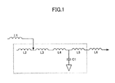
- Figure 1 is an equivalent circuit schematic showing the configuration of an impedance matching device according to the present example.
- Components inside the tetragonal frame depicted with dotted line in Figure 1 represent components included in the impedance matching device according to the present example.
- L1 and L6 are components not included in the impedance matching device according to the present example, and specifically represent metal wires for connecting the impedance matching device according to the present example and another device (for example, an external circuit such as high frequency wave semiconductor amplifier).
- L4 and L5 represent inductor portions embedded inside the first dielectric material D1 (not shown in Figure 1 ) in the impedance matching device according to the present example.
- the capacitor portion C1 is connected, and the other end of the capacitor portion C1 is connected to the ground electrode.
- the second dielectric material D2 (not shown in Figure 1 ) with a dielectric constant higher than that of the first dielectric material D1 intermediates.
- L2 and L3 schematically show the inductances presented by one electrode for bonding E1 (not shown in Figure 1 ) of the impedance matching device according to the present example. It is represented that, as mentioned in the explanation about the impedance matching device according to the previously mentioned sixth embodiment, depending on at which point on the electrode for bonding E1 the metal wire L1 for connecting the impedance matching device according to the present example and another device is bonded, the inductance presented by the electrode for bonding E1 varies.
- One end of the above-described electrode for bonding E1 is connected to the end, which is on the opposite side to the inductor portion L5, of the inductor portion L4.
- another electrode for bonding E2 (not shown in Figure 1 ) is connected and the metal wire L6 is connected to the electrode E2.
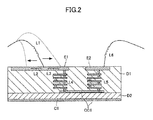
- FIG. 2 is a cross-section view showing the schematic configuration of an impedance matching device according to the present example.
- the inductor portions L4 and L5 respectively comprising a conductor pattern for inductor in a coil-like shape are embedded inside the first dielectric material D1.
- a pair of the conductor patterns for capacitor CC1 is formed so as to sandwich the second dielectric material D2 laminated below the first dielectric material D1 and constitutes the capacitor portion C1.
- the second dielectric material D2 has a higher dielectric constant than the first dielectric material D1.
- the electrodes for bonding E1 and E2 are formed so as to expose in surface identical to the upper surface of the first dielectric material D1.
- the conductor patterns (to which reference signs are not assigned) embedded inside the first dielectric material D1 connect the electrode for bonding E1, the inductor portion L4, the inductor portion L5, and the electrode for bonding E2 in this order and in series.
- the upper conductor pattern for capacitor of a pair of the conductor patterns for capacitor CC1 included in the capacitor portion C1 is connected, and the lower conductor pattern for capacitor facing the upper conductor pattern for capacitor across the second dielectric material D2 doubles as a ground electrode.
- the impedance matching device comprises two inductor portions and one capacitor portion
- the size of the whole device is successfully decreased by equipping, as an integrally molded body, these components, as well as the first and second dielectric materials.
- by manufacturing as such an integrally molded body as compared with a conventional impedance matching circuit manufactured by connecting an inductor consisting of metal fine line having given length and curvature etc with a capacitor, variation in inductance and the like can be suppressed.
- the impedance matching device according to the present invention should be low-resistant and low loss even when it is connected with a high power high frequency wave device as mentioned previously, the thicknesses of said conductor pattern for wiring and the conductor patterns constituting said inductor portions L4 and L5 are desirably 20 ⁇ m or more, more preferably 30 ⁇ m or more.
- the electrode for bonding E1 in accordance with at which point on the electrode for bonding E1 the metal wire for connecting the impedance matching device according to the present example and another device is bonded (represented by the arrows in Figure 2 ), the inductance presented by the electrode for bonding E1 varies. Thereby, the inductance of the portion obtained by combining the inductor portion L4 and the electrode for bonding E1, which exists on the left side from the capacitor portion C1, can be adjusted.
- conductor components themselves such as metal wire and metal ribbon, for electrically connecting the impedance matching device according to the present invention and another device can be inductors.
- the metal wires for connecting the impedance matching device according to the present example and another device are represented as the inductor portions L1 and L6.
- the impedance matching device according to the present example is connected with another device, it may be necessary to be configured so that the combination of the inductance of the conductor component and the inductance of the electrode for bonding, the wiring portion, the inductor portion and/or the inductor portion for adjustment of the impedance matching device comes to a desired inductance value.
- the configuration of the impedance matching device according to the present example corresponds to the impedance matching devices according to the previously mentioned sixth and eleventh embodiments.
- An impedance matching device with such a configuration can be obtained by manufacturing a ceramic powder compact with a conductor powder compact embedded therein, drying and thereafter firing the resulting ceramic powder compact as mentioned previously.
- the above-described method is not more than an example, and a method for manufacturing the impedance matching device according to the present invention is not limited to the above-described method.
- the metal wire itself for electrically connecting the impedance matching device according to the present example and another device is taken into account as an inductor.
- the impedance matching device succeeds in with a small variation in quality, large-current tolerance, and downsizing of the whole device by its configuration as mentioned above.
- the present invention can be suitably applied to a high frequency wave power amplifier used in, for example, a base transceiver station for mobile-phones, an industrial radio-frequency heating apparatus and the like.
- a base transceiver station for mobile-phones for example, a base transceiver station for mobile-phones, an industrial radio-frequency heating apparatus and the like.
- the present invention is not limited to these applications.
- L1 metal wire (its equivalent inductance being taken into account)
- L2 part of electrode for bonding E1 (its equivalent inductance being taken into account)
- L3 part of electrode for bonding E1 (its equivalent inductance being taken into account)
- L4 inductor portion
- L5 inductor portion
- L6 metal wire (its equivalent inductance being taken into account)
- C1 capacitor portion
- CC1 conductor pattern for capacitor
- E1 electrode for bonding
- E2 electrode for bonding
- D1 first dielectric material
- D2 second dielectric material.
Landscapes
- Engineering & Computer Science (AREA)
- Power Engineering (AREA)
- Microelectronics & Electronic Packaging (AREA)
- Coils Or Transformers For Communication (AREA)
- Fixed Capacitors And Capacitor Manufacturing Machines (AREA)
Applications Claiming Priority (2)
| Application Number | Priority Date | Filing Date | Title |
|---|---|---|---|
| US34925410P | 2010-05-28 | 2010-05-28 | |
| PCT/JP2011/061231 WO2011148819A1 (ja) | 2010-05-28 | 2011-05-16 | インピーダンス整合素子 |
Publications (2)
| Publication Number | Publication Date |
|---|---|
| EP2579459A1 true EP2579459A1 (de) | 2013-04-10 |
| EP2579459A4 EP2579459A4 (de) | 2016-11-16 |
Family
ID=45003810
Family Applications (1)
| Application Number | Title | Priority Date | Filing Date |
|---|---|---|---|
| EP11786518.8A Withdrawn EP2579459A4 (de) | 2010-05-28 | 2011-05-16 | Impedanzanpassungselement |
Country Status (5)
| Country | Link |
|---|---|
| US (1) | US8878625B2 (de) |
| EP (1) | EP2579459A4 (de) |
| JP (1) | JPWO2011148819A1 (de) |
| CN (1) | CN102986138B (de) |
| WO (1) | WO2011148819A1 (de) |
Families Citing this family (10)
| Publication number | Priority date | Publication date | Assignee | Title |
|---|---|---|---|---|
| US8659359B2 (en) | 2010-04-22 | 2014-02-25 | Freescale Semiconductor, Inc. | RF power transistor circuit |
| KR101304316B1 (ko) * | 2011-12-15 | 2013-09-11 | 전자부품연구원 | 본딩 와이어 임피던스 정합회로 |
| US9281283B2 (en) | 2012-09-12 | 2016-03-08 | Freescale Semiconductor, Inc. | Semiconductor devices with impedance matching-circuits |
| KR101771749B1 (ko) * | 2012-12-28 | 2017-08-25 | 삼성전기주식회사 | 인덕터 |
| US10432152B2 (en) | 2015-05-22 | 2019-10-01 | Nxp Usa, Inc. | RF amplifier output circuit device with integrated current path, and methods of manufacture thereof |
| US9692363B2 (en) | 2015-10-21 | 2017-06-27 | Nxp Usa, Inc. | RF power transistors with video bandwidth circuits, and methods of manufacture thereof |
| US9571044B1 (en) | 2015-10-21 | 2017-02-14 | Nxp Usa, Inc. | RF power transistors with impedance matching circuits, and methods of manufacture thereof |
| CN115149924A (zh) * | 2016-06-27 | 2022-10-04 | 株式会社村田制作所 | 滤波器装置 |
| WO2018110054A1 (ja) * | 2016-12-12 | 2018-06-21 | 株式会社村田製作所 | Lcデバイス、lcデバイスの製造方法 |
| US11783992B2 (en) * | 2019-09-06 | 2023-10-10 | Cyntec Co., Ltd. | Integrally-formed inductor and a fabricatin method thereof |
Family Cites Families (16)
| Publication number | Priority date | Publication date | Assignee | Title |
|---|---|---|---|---|
| JPS62152134A (ja) | 1985-12-25 | 1987-07-07 | Mitsubishi Electric Corp | 内部整合回路付半導体装置 |
| JPH01220842A (ja) | 1988-02-29 | 1989-09-04 | Nec Corp | 半導体内部整合装置 |
| JPH0258816A (ja) | 1988-08-24 | 1990-02-28 | Matsushita Electric Ind Co Ltd | 積層セラミック電子部品の製造方法 |
| JPH0685593A (ja) * | 1992-08-28 | 1994-03-25 | Mitsubishi Electric Corp | 高周波整合用回路装置 |
| US5903198A (en) * | 1997-07-30 | 1999-05-11 | Massachusetts Institute Of Technology | Planar gyrator |
| JP2000058580A (ja) * | 1998-08-13 | 2000-02-25 | Nec Corp | ボンディングパッドを有する半導体装置 |
| JP3494120B2 (ja) * | 2000-04-28 | 2004-02-03 | 株式会社村田製作所 | 積層型lc部品 |
| JP2003133882A (ja) * | 2001-08-16 | 2003-05-09 | Murata Mfg Co Ltd | インピーダンス整合素子 |
| JP2004221572A (ja) * | 2002-12-27 | 2004-08-05 | Tdk Corp | 電子部品及び多層基板 |
| JP4217106B2 (ja) * | 2003-05-23 | 2009-01-28 | パナソニック株式会社 | モノリシックマイクロ波集積回路 |
| EP1652264A1 (de) * | 2003-07-28 | 2006-05-03 | Philips Intellectual Property & Standards GmbH | Hochfrequenzkomponente |
| US7187249B2 (en) * | 2004-09-24 | 2007-03-06 | Avago Technologies Wireless Ip (Singapore) Pte. Ltd. | Interconnecting a port of a microwave circuit package and a microwave component mounted in the microwave circuit package |
| JP2006286931A (ja) * | 2005-03-31 | 2006-10-19 | Tdk Corp | 薄膜デバイス |
| JP2007110042A (ja) * | 2005-10-17 | 2007-04-26 | Sony Corp | 受動素子及びその製造方法、受動素子の実装構造及びその実装方法 |
| JP2009016698A (ja) | 2007-07-09 | 2009-01-22 | Rohm Co Ltd | フォトリフレクタ |
| WO2009016698A1 (ja) | 2007-07-27 | 2009-02-05 | Ngk Insulators, Ltd. | セラミック粉末成形体、セラミック焼成体及びセラミック粉末成形体の製造方法 |
-
2011
- 2011-05-16 JP JP2012517221A patent/JPWO2011148819A1/ja not_active Withdrawn
- 2011-05-16 CN CN201180034330.7A patent/CN102986138B/zh not_active Expired - Fee Related
- 2011-05-16 EP EP11786518.8A patent/EP2579459A4/de not_active Withdrawn
- 2011-05-16 WO PCT/JP2011/061231 patent/WO2011148819A1/ja not_active Ceased
- 2011-05-25 US US13/115,396 patent/US8878625B2/en not_active Expired - Fee Related
Also Published As
| Publication number | Publication date |
|---|---|
| EP2579459A4 (de) | 2016-11-16 |
| US20120019334A1 (en) | 2012-01-26 |
| CN102986138B (zh) | 2015-07-01 |
| JPWO2011148819A1 (ja) | 2013-07-25 |
| CN102986138A (zh) | 2013-03-20 |
| US8878625B2 (en) | 2014-11-04 |
| WO2011148819A1 (ja) | 2011-12-01 |
Similar Documents
| Publication | Publication Date | Title |
|---|---|---|
| US8878625B2 (en) | Impedance matching device | |
| US11594378B2 (en) | Electronic component and electronic component device | |
| US10297390B2 (en) | Electronic component | |
| US7430107B2 (en) | Monolithic capacitor, circuit board, and circuit module | |
| US12273990B2 (en) | High-frequency board, high-frequency package, and high-frequency module | |
| JP7025504B2 (ja) | 高周波基体、高周波パッケージおよび高周波モジュール | |
| US9609743B2 (en) | Electronic device mounting substrate, electronic apparatus, and imaging module | |
| CN205680518U (zh) | 电感器以及频带去除滤波器 | |
| WO2017179590A1 (ja) | 受動素子アレイおよびプリント配線板 | |
| JP2019079865A (ja) | 電子部品 | |
| US20190006076A1 (en) | Inductor module | |
| CN110337718B (zh) | 绝缘基体、半导体封装以及半导体装置 | |
| KR102558332B1 (ko) | 인덕터 및 이의 제조 방법 | |
| EP4600998A1 (de) | Leiterplatte, gehäuse zur montage elektronischer komponenten mit der leiterplatte und elektronisches modul | |
| JP2004153414A (ja) | ローパスフィルタ | |
| JP6809813B2 (ja) | 半導体パッケージおよび半導体装置 | |
| JP6502826B2 (ja) | 配線基板および高周波モジュール | |
| JP2009272510A (ja) | Icパッケージの実装構造、その製造方法およびそのためのシートキャパシタ | |
| KR100543411B1 (ko) | 고주파 통신 모듈의 패키징 장치 및 그 제조 방법 | |
| JP2011250402A (ja) | 高調波抑制用オープンスタブを有するインピーダンス整合素子 | |
| JP2006269724A (ja) | セラミックデバイス | |
| JP2006156551A (ja) | Lc複合部品 | |
| JP2006156552A (ja) | Lc複合部品 |
Legal Events
| Date | Code | Title | Description |
|---|---|---|---|
| PUAI | Public reference made under article 153(3) epc to a published international application that has entered the european phase |
Free format text: ORIGINAL CODE: 0009012 |
|
| 17P | Request for examination filed |
Effective date: 20121227 |
|
| AK | Designated contracting states |
Kind code of ref document: A1 Designated state(s): AL AT BE BG CH CY CZ DE DK EE ES FI FR GB GR HR HU IE IS IT LI LT LU LV MC MK MT NL NO PL PT RO RS SE SI SK SM TR |
|
| DAX | Request for extension of the european patent (deleted) | ||
| RIC1 | Information provided on ipc code assigned before grant |
Ipc: H01F 17/02 20060101ALI20160707BHEP Ipc: H03H 7/38 20060101AFI20160707BHEP Ipc: H01F 17/00 20060101ALN20160707BHEP |
|
| RA4 | Supplementary search report drawn up and despatched (corrected) |
Effective date: 20161017 |
|
| RIC1 | Information provided on ipc code assigned before grant |
Ipc: H03H 7/38 20060101AFI20161011BHEP Ipc: H01F 17/00 20060101ALN20161011BHEP Ipc: H01F 17/02 20060101ALI20161011BHEP |
|
| STAA | Information on the status of an ep patent application or granted ep patent |
Free format text: STATUS: THE APPLICATION HAS BEEN WITHDRAWN |
|
| 18W | Application withdrawn |
Effective date: 20170126 |