EP2579313A1 - Organic light emitting diode display device and method of fabricating the same - Google Patents
Organic light emitting diode display device and method of fabricating the same Download PDFInfo
- Publication number
- EP2579313A1 EP2579313A1 EP20120006623 EP12006623A EP2579313A1 EP 2579313 A1 EP2579313 A1 EP 2579313A1 EP 20120006623 EP20120006623 EP 20120006623 EP 12006623 A EP12006623 A EP 12006623A EP 2579313 A1 EP2579313 A1 EP 2579313A1
- Authority
- EP
- European Patent Office
- Prior art keywords
- layer
- light emitting
- thin film
- transport layer
- emitting layer
- Prior art date
- Legal status (The legal status is an assumption and is not a legal conclusion. Google has not performed a legal analysis and makes no representation as to the accuracy of the status listed.)
- Granted
Links
Images




Classifications
-
- H—ELECTRICITY
- H10—SEMICONDUCTOR DEVICES; ELECTRIC SOLID-STATE DEVICES NOT OTHERWISE PROVIDED FOR
- H10K—ORGANIC ELECTRIC SOLID-STATE DEVICES
- H10K59/00—Integrated devices, or assemblies of multiple devices, comprising at least one organic light-emitting element covered by group H10K50/00
- H10K59/30—Devices specially adapted for multicolour light emission
- H10K59/35—Devices specially adapted for multicolour light emission comprising red-green-blue [RGB] subpixels
-
- H—ELECTRICITY
- H10—SEMICONDUCTOR DEVICES; ELECTRIC SOLID-STATE DEVICES NOT OTHERWISE PROVIDED FOR
- H10K—ORGANIC ELECTRIC SOLID-STATE DEVICES
- H10K50/00—Organic light-emitting devices
- H10K50/10—OLEDs or polymer light-emitting diodes [PLED]
- H10K50/11—OLEDs or polymer light-emitting diodes [PLED] characterised by the electroluminescent [EL] layers
-
- H—ELECTRICITY
- H10—SEMICONDUCTOR DEVICES; ELECTRIC SOLID-STATE DEVICES NOT OTHERWISE PROVIDED FOR
- H10K—ORGANIC ELECTRIC SOLID-STATE DEVICES
- H10K50/00—Organic light-emitting devices
- H10K50/10—OLEDs or polymer light-emitting diodes [PLED]
- H10K50/14—Carrier transporting layers
- H10K50/15—Hole transporting layers
-
- H—ELECTRICITY
- H10—SEMICONDUCTOR DEVICES; ELECTRIC SOLID-STATE DEVICES NOT OTHERWISE PROVIDED FOR
- H10K—ORGANIC ELECTRIC SOLID-STATE DEVICES
- H10K50/00—Organic light-emitting devices
- H10K50/10—OLEDs or polymer light-emitting diodes [PLED]
- H10K50/14—Carrier transporting layers
- H10K50/16—Electron transporting layers
-
- H—ELECTRICITY
- H10—SEMICONDUCTOR DEVICES; ELECTRIC SOLID-STATE DEVICES NOT OTHERWISE PROVIDED FOR
- H10K—ORGANIC ELECTRIC SOLID-STATE DEVICES
- H10K50/00—Organic light-emitting devices
- H10K50/10—OLEDs or polymer light-emitting diodes [PLED]
- H10K50/17—Carrier injection layers
-
- H—ELECTRICITY
- H10—SEMICONDUCTOR DEVICES; ELECTRIC SOLID-STATE DEVICES NOT OTHERWISE PROVIDED FOR
- H10K—ORGANIC ELECTRIC SOLID-STATE DEVICES
- H10K50/00—Organic light-emitting devices
- H10K50/10—OLEDs or polymer light-emitting diodes [PLED]
- H10K50/17—Carrier injection layers
- H10K50/171—Electron injection layers
-
- H—ELECTRICITY
- H10—SEMICONDUCTOR DEVICES; ELECTRIC SOLID-STATE DEVICES NOT OTHERWISE PROVIDED FOR
- H10K—ORGANIC ELECTRIC SOLID-STATE DEVICES
- H10K50/00—Organic light-emitting devices
- H10K50/80—Constructional details
- H10K50/805—Electrodes
- H10K50/82—Cathodes
- H10K50/828—Transparent cathodes, e.g. comprising thin metal layers
-
- H—ELECTRICITY
- H10—SEMICONDUCTOR DEVICES; ELECTRIC SOLID-STATE DEVICES NOT OTHERWISE PROVIDED FOR
- H10K—ORGANIC ELECTRIC SOLID-STATE DEVICES
- H10K59/00—Integrated devices, or assemblies of multiple devices, comprising at least one organic light-emitting element covered by group H10K50/00
- H10K59/30—Devices specially adapted for multicolour light emission
- H10K59/35—Devices specially adapted for multicolour light emission comprising red-green-blue [RGB] subpixels
- H10K59/353—Devices specially adapted for multicolour light emission comprising red-green-blue [RGB] subpixels characterised by the geometrical arrangement of the RGB subpixels
-
- H—ELECTRICITY
- H10—SEMICONDUCTOR DEVICES; ELECTRIC SOLID-STATE DEVICES NOT OTHERWISE PROVIDED FOR
- H10K—ORGANIC ELECTRIC SOLID-STATE DEVICES
- H10K71/00—Manufacture or treatment specially adapted for the organic devices covered by this subclass
-
- H—ELECTRICITY
- H10—SEMICONDUCTOR DEVICES; ELECTRIC SOLID-STATE DEVICES NOT OTHERWISE PROVIDED FOR
- H10K—ORGANIC ELECTRIC SOLID-STATE DEVICES
- H10K71/00—Manufacture or treatment specially adapted for the organic devices covered by this subclass
- H10K71/10—Deposition of organic active material
-
- H—ELECTRICITY
- H10—SEMICONDUCTOR DEVICES; ELECTRIC SOLID-STATE DEVICES NOT OTHERWISE PROVIDED FOR
- H10K—ORGANIC ELECTRIC SOLID-STATE DEVICES
- H10K71/00—Manufacture or treatment specially adapted for the organic devices covered by this subclass
- H10K71/20—Changing the shape of the active layer in the devices, e.g. patterning
- H10K71/221—Changing the shape of the active layer in the devices, e.g. patterning by lift-off techniques
-
- H—ELECTRICITY
- H10—SEMICONDUCTOR DEVICES; ELECTRIC SOLID-STATE DEVICES NOT OTHERWISE PROVIDED FOR
- H10K—ORGANIC ELECTRIC SOLID-STATE DEVICES
- H10K71/00—Manufacture or treatment specially adapted for the organic devices covered by this subclass
- H10K71/20—Changing the shape of the active layer in the devices, e.g. patterning
- H10K71/231—Changing the shape of the active layer in the devices, e.g. patterning by etching of existing layers
- H10K71/233—Changing the shape of the active layer in the devices, e.g. patterning by etching of existing layers by photolithographic etching
-
- H—ELECTRICITY
- H10—SEMICONDUCTOR DEVICES; ELECTRIC SOLID-STATE DEVICES NOT OTHERWISE PROVIDED FOR
- H10H—INORGANIC LIGHT-EMITTING SEMICONDUCTOR DEVICES HAVING POTENTIAL BARRIERS
- H10H20/00—Individual inorganic light-emitting semiconductor devices having potential barriers, e.g. light-emitting diodes [LED]
- H10H20/80—Constructional details
- H10H20/81—Bodies
- H10H20/819—Bodies characterised by their shape, e.g. curved or truncated substrates
-
- H—ELECTRICITY
- H10—SEMICONDUCTOR DEVICES; ELECTRIC SOLID-STATE DEVICES NOT OTHERWISE PROVIDED FOR
- H10H—INORGANIC LIGHT-EMITTING SEMICONDUCTOR DEVICES HAVING POTENTIAL BARRIERS
- H10H20/00—Individual inorganic light-emitting semiconductor devices having potential barriers, e.g. light-emitting diodes [LED]
- H10H20/80—Constructional details
- H10H20/85—Packages
- H10H20/857—Interconnections, e.g. lead-frames, bond wires or solder balls
-
- H—ELECTRICITY
- H10—SEMICONDUCTOR DEVICES; ELECTRIC SOLID-STATE DEVICES NOT OTHERWISE PROVIDED FOR
- H10H—INORGANIC LIGHT-EMITTING SEMICONDUCTOR DEVICES HAVING POTENTIAL BARRIERS
- H10H29/00—Integrated devices, or assemblies of multiple devices, comprising at least one light-emitting semiconductor element covered by group H10H20/00
- H10H29/10—Integrated devices comprising at least one light-emitting semiconductor component covered by group H10H20/00
- H10H29/14—Integrated devices comprising at least one light-emitting semiconductor component covered by group H10H20/00 comprising multiple light-emitting semiconductor components
-
- H—ELECTRICITY
- H10—SEMICONDUCTOR DEVICES; ELECTRIC SOLID-STATE DEVICES NOT OTHERWISE PROVIDED FOR
- H10K—ORGANIC ELECTRIC SOLID-STATE DEVICES
- H10K59/00—Integrated devices, or assemblies of multiple devices, comprising at least one organic light-emitting element covered by group H10K50/00
- H10K59/80—Constructional details
- H10K59/805—Electrodes
- H10K59/8052—Cathodes
- H10K59/80524—Transparent cathodes, e.g. comprising thin metal layers
Definitions
- the present invention relates to organic light emitting diode (OLED) display device and a method of fabricating the same and, more particularly, to an OLED display device in which OLED pixels are patterned through a photolithography process, and a method of fabricating the same.
- OLED organic light emitting diode
- FPDs flat panel displays
- CRTs cathode ray tubes
- LCD liquid crystal display
- An LED display device one of new display devices, is a self-luminous type device, which thus is excellent in a viewing angle and contrast ratio, is lighter and thinner because it does not need a backlight, and is advantageous in terms of power consumption, relative to an LCD device.
- an OLED display device can be driven by a DC and at a low voltage, has a fast response speed, and is especially advantageous in terms of fabrication costs.
- deposition and encapsulation are the whole of a fabrication process of an OLED display device, so the fabrication process is very simple. Also, when the OLED display device is driven according to an active matrix scheme in which each pixel has a thin film transistor (TFT) as a switching element, the same luminance can be obtained although a low current is applied, so, advantageously, the OLED display device consumes low power, has a high pitch (or high definition or high resolution), and can be increased in size.
- TFT thin film transistor
- FIG. 1 is a diagram illustrating a light emission principle of a general OLED display device.
- a general OLED display device includes an OLED.
- the OLED includes organic compound layers 301, 30b, 30c, 30d, and 30e formed between an anode 18 as a pixel electrode and a cathode 28 as a common electrode.
- the organic compound layers 30a, 30b, 30c, 30d, and 30e include a hole injection layer 30a, a hole transport layer 30b, an emission layer 30c, an electron transport layer 30d, and an electron injection layer 30e.
- the pixels each having the OLED having the foregoing structure are arranged in a matrix form and selectively controlled by a data voltage and a scan voltage to display an image.
- the OLED display device is divided into a passive matrix type OLED display device and an active matrix type display device using TFTs as switching elements.
- TFTs as active elements are selectively turned on to select pixels and emitting of pixels is maintained by a voltage maintained in a storage capacitor.
- FIG. 2 is an equivalent circuit diagram of a pixel in a general OLED display device. Namely, FIG. 2 illustrates an example of an equivalent circuit diagram of a pixel having a general 2T1C (including two transistors and one capacitor) in an active matrix type OLED display device.
- a general 2T1C including two transistors and one capacitor
- a pixel of an active matrix type OLED display device includes an OLED, a data line DL and a gate line GL crossing each other, a switching TFT SW, a driving TFT DR, and a storage capacitor Cst.
- the switching TFT SW is turned on in response to a scan pulse from the gate line GL to conduct a current path between a source electrode and a drain electrode thereof.
- a data voltage from the data line DL is applied to a gate electrode of the driving TFT DR and the storage capacitor Cst by way of the source electrode and drain electrode of the switching TFT SW.
- the driving TFT DR controls a current flowing in the OLED according to the data voltage applied to the gate electrode thereof.
- the storage capacitor Cst stores a voltage between the data voltage and a low potential power source voltage VSS and uniformly maintains it during one frame period.
- a mask or a shadow mask or a fine metal mask (FMM) having a plurality of openings corresponding to a plurality of pixel regions is used.
- this method has a limitation in that it is not easy to cope with a fine pitch of patterns for increasing a size of a substrate and implementing a high resolution display
- FMM is fabricated by forming holes as a pattern intended for deposition on a thin metal plate and stretching the same.
- a pattern having a small size making it difficult to reduce the size of an OLED.
- warpage occurs due to the characteristics of the fine metal mask, distort the pattern to degrade a production yield.
- An aspect of the present invention provides an organic light emitting diode (OLED) display device in which OLED pixels are patterned through a photolithography process, thus being available for large area patterning and obtaining a high pitch (or high definition or high resolution), and a method for fabricating the same.
- OLED organic light emitting diode
- Another aspect of the present invention provides an OLED display device in which a light emitting layer is protected during a patterning process through photolithography, and a method for fabricating the same.
- Another aspect of the present invention provides an OLED display device capable of simplifying a process and increasing efficiency, and a method for fabricating the same.
- an organic light emitting diode (OLED) display device including: a first electrode formed on a substrate; a hole injection layer and a hole transport layer formed on the substrate with the first electrode formed thereon; a first light emitting layer formed of a first organic film on the substrate with the hole injection layer and the hole transport layer formed thereon; a second light emitting layer formed of a second organic film on the substrate with the first light emitting layer formed thereon; a third light emitting layer formed by depositing a third organic film on the entire surface of the substrate with the first light emitting layer and the second light emitting layer formed thereon; and an electron injection layer and a second electrode formed on the third light emitting layer.
- OLED organic light emitting diode
- the third light emitting layer may be formed on upper portions of the first light emitting layer and the second light emitting layer as well as between the first light emitting layer and the second light emitting layer.
- an organic light emitting diode (OLED) display device including: a first electrode formed on a substrate; a first hole injection layer, a first hole transport layer, a first light emitting layer, a first electron transport layer, and a first buffer layer laminated on the substrate; a second hole injection layer, a second hole transport layer, a second light emitting layer, a second electron transport layer, and a second buffer layer laminated on the substrate; a third hole injection layer, a third hole transport layer, a third light emitting layer, a third electron transport layer, and a third buffer layer laminated on the substrate; and a second electrode formed on the first, second, and third buffer layers, wherein the first, second, and third buffer layers are made of a metal oxide.
- the first, second, and third buffer layers may be made of a 1-2 Group and 12-16 Group metal oxide or 3-12 Group transition metal oxide.
- a method for fabricating an organic light emitting diode (OLED) display device including: forming a first electrode on a substrate; forming a first light emitting layer formed of a first organic film on the substrate through a first photo process; forming a second light emitting layer formed of a second organic film on the substrate through a second photo process; depositing a third organic film on first and second photosensitive resin patterns remaining after being used during the first and second photo processes; removing the third organic film deposited on upper portions of the first and second photosensitive resin patterns together with the first and second photosensitive resin patterns through a lift-off process to form a third light emitting layer; and forming a second electrode on the first, second, and third light emitting layers.
- OLED organic light emitting diode
- a method for fabricating an organic light emitting diode (OLED) display device including: (a) forming a first electrode on a substrate; (b) applying a photosensitive resin to the entire surface of the substrate to form a first photosensitive resin layer; (c) selectively exposing and developing the first photosensitive resin layer to form a first photosensitive resin pattern made of the photosensitive resin at a position other than a position where a first light emitting layer is to be formed; (d) depositing a first organic film on the first photosensitive resin pattern in a state in which the first photosensitive resin pattern remains; (e) removing the first organic film deposited on an upper portion of the first photosensitive resin pattern together with the first photosensitive resin pattern through a lift-off process to form a first light emitting layer formed of the first organic film on the substrate; (f) forming a second light emitting layer formed of a second organic film on the substrate through the same processes as (b) to (e); (g) depositing a
- the third light emitting layer may be formed between the first light emitting layer and the second light emitting layer.
- the third light emitting layer may be formed on upper portions of the first light emitting layer and the second light emitting layer as well as between the first light emitting layer and the second light emitting layer.
- the first light emitting layer may be formed thereon.
- the first light emitting layer may be formed as any one of red, green, and blue light emitting layers.
- the second light emitting layer may be formed as another one of the red, green, and blue light emitting layers.
- the third light emitting layer may be formed as the other remaining one of the red, green, and blue light emitting layers.
- the second electrode may be formed thereon.
- a method for fabricating an organic light emitting diode (OLED) display device including: forming a first electrode on a substrate; forming a first hole injection layer, a first hole transport layer, a first light emitting layer, a first electron transport layer, and a first buffer layer in a laminated manner on the substrate through a first photo process; forming a second hole injection layer, a second hole transport layer, a second light emitting layer, a second electron transport layer, and a second buffer layer in a laminated manner on the substrate through a first photo process; forming a third hole injection layer, a third hole transport layer, a third light emitting layer, a third electron transport layer, and a third buffer layer in a laminated manner on the substrate through a first photo process; and forming a second electrode on the first, second, and third buffer layers, wherein the first, second, and third buffer layers are made of a metal oxide.
- a method for fabricating an organic light emitting diode (OLED) display device including: (a) forming a first electrode on a substrate; (b) applying a photosensitive resin to the entire surface of the substrate to form a first photosensitive resin layer; (c) selectively exposing and developing the first photosensitive resin layer to form a first photosensitive resin pattern made of the photosensitive resin at a position other than a position where a first light emitting layer is to be formed; (d) depositing a thin film for a first hole injection layer, a thin film for a first hole transport layer, a first organic film, a thin film for a first electron transport layer, and a thin film for a first buffer layer in a state in which the first photosensitive resin pattern remains; (e) removing the thin film for a first hole injection layer, the thin film for a first hole transport layer, the first organic film, the thin film for a first electron transport layer, and the thin film for a first buffer layer deposited on
- the forming of the first hole injection layer, the first hole transport layer, the first light emitting layer, the first electron transport layer, and the first buffer layer may include: depositing a thin film for a first hole injection layer, a thin film for a first hole transport layer, a first organic film, a thin film for a first electron transport layer, and a thin film for a first buffer layer on the substrate; applying a photosensitive resin to the entire surface of the substrate with the thin film for a first hole injection layer, the thin film for a first hole transport layer, the first organic film, the thin film for a first electron transport layer, and the thin film for a first buffer layer deposited thereon to form a first photosensitive resin layer; exposing and developing the first photosensitive resin layer to from a first photosensitive resin pattern made of the photosensitive resin at a position where a first light emitting is to be formed; and selectively etching the thin film for a first hole injection layer, the thin film for a first hole transport layer, the first organic film, the thin film for a first electron
- the forming of the second hole injection layer, the second hole transport layer, the second light emitting layer, the second electron transport layer, and the second buffer layer may include: depositing a thin film for a second hole injection layer, a thin film for a second hole transport layer, a second organic film, a thin film for a second electron transport layer, and a thin film for a second buffer layer on the substrate; applying a photosensitive resin to the entire surface of the substrate with the thin film for a second hole injection layer, the thin film for a second hole transport layer, the second organic film, the thin film for a second electron transport layer, and the thin film for a second buffer layer deposited thereon to form a second photosensitive resin layer; exposing and developing the second photosensitive resin layer to from a second photosensitive resin pattern made of the photosensitive resin at a position where a second light emitting is to be formed; and selectively etching the thin film for a second hole injection layer, the thin film for a second hole transport layer, the second organic film, the thin film for a second electron
- the forming of the third hole injection layer, the third hole transport layer, the third light emitting layer, the third electron transport layer, and the third buffer layer may include: depositing a thin film for a third hole injection layer, a thin film for a third hole transport layer, a third organic film, a thin film for a third electron transport layer, and a thin film for a third buffer layer on the substrate; applying a photosensitive resin to the entire surface of the substrate with the thin film for a third hole injection layer, the thin film for a third hole transport layer, the third organic film, the thin film for a third electron transport layer, and the thin film for a third buffer layer deposited thereon to form a third photosensitive resin layer; exposing and developing the third photosensitive resin layer to from a third photosensitive resin pattern made of the photosensitive resin at a position where a third light emitting is to be formed; and selectively etching the thin film for a third hole injection layer, the thin film for a third hole transport layer, the third organic film, the thin film for a third electron
- the first, second, and third buffer layers may be made of a 1-2 Group and 12-16 Group metal oxide or 3-12 Group transition metal oxide.
- a method for fabricating an organic light emitting diode (OLED) display device including: (a) forming a fourth electrode on a substrate; (b) forming a first organic film and a first conductive film on the substrate with the fourth electrode formed thereon; (c) applying a photosensitive resin to the entire surface of the substrate with the first conductive film formed thereon to form a first photosensitive resin layer; (d) selectively exposing and developing the first photosensitive resin layer to form a first photosensitive resin pattern made of the photosensitive resin at a position at which a first light emitting is to be formed; (e) selectively removing the first conductive film by using the first photosensitive resin pattern as a mask to form a first electrode; (f) removing the first photosensitive resin pattern and selectively removing the underlying exposed first organic film by using the first electrode as a mask to form a first light emitting layer formed of the first organic film; (g) forming a second light emitting layer and a second electrode
- the first organic film may be formed, and after a thin film for a first electron transport layer is formed, the first conductive film may be formed.
- OLED pixels are patterned through a photolithography process, a large area patterning can be performed and a fine pitch can be obtained, and an organic compound layer can be protected by forming a buffer layer of a metal oxide on an upper portion of the organic compound layer or patterning the organic compound layer by using a cathode as a mask, improving device efficiency.
- patterning through a photolithography process can be performed through a solution process, and since a light emitting layer is protected during a patterning process, a driving voltage and power consumption of the device can be reduced and efficiency can be enhanced.
- the process can be simplified and efficiency can be increased.
- OLED organic light emitting diode
- a method for fabricating the same according to embodiments of the present invention will be described in detail with reference to the accompanying drawings such that they can be easily implemented by a person skilled in the art to which the present invention pertains.
- the present invention may be implemented in various forms without being limited to the embodiments described herein. Patterning of a large area with respect to an organic compound layer of an OLED display device cannot be handled by an existing method using a fine metal mask due to sagging of a substrate and a mask, so various large area patterning methods have been researched.
- the present invention proposes a patterning method through a photolithography process (referred to as a 'photo process', hereinafter), and here, the photo process is advantageous in that it is available for large area patterning and obtaining a fine pitch, and available for an application of a solution process.
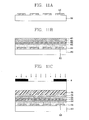
- FIGS. 3A through 3L are sequential sectional views illustrating a method for fabricating an OLED display device according to a first embodiment of the present invention, in which a method for fabricating an OLED diode with respect to some pixels is taken as an example.
- a gate line including a first gate electrode and a storage electrode including a second gate electrode may be formed on a substrate 110 made of an insulating material such as transparent glass, plastic, or the like.
- a gate insulating layer made of silicon nitride (SiNx), silicon oxide (SiO 2 ), or the like, may be formed on the gate line including the first gate electrode and the storage electrode including the second electrode.
- a first active layer and a second active layer, made of semiconductor, may be formed on the gate insulating layer.
- the first active layer and the second active layer may be positioned on the first gate electrode and the second gate electrode, respectively.
- a data line, a driving voltage line, a first source/drain electrode, and a second source/drain electrode may be formed on an upper portion of the first active layer and the second active layer.
- a predetermined passivation layer may be formed on the substrate 110 on which the data line, the driving voltage line, the first source/drain electrode, and the second source/drain electrode have been formed.
- a pixel electrode 120 and a connecting electrode may be formed on the substrate 110 with the passivation film formed thereon.
- the pixel electrode 120 and the connecting electrode may be made of a transparent conductive material such as indium tin oxide (ITO) or a reflective conductive material such as aluminum, silver, or an alloy thereof.
- the pixel electrode 120 as an anode may be electrically connected to the second drain electrode through a second contact hole, and the connecting electrode may electrically connect the first drain electrode and the second gate electrode through a first contact hole and a third contact hole.
- a partition may be formed on the substrate 110 with the pixel electrode 120 formed thereon.
- the partition may encompass the edges of the pixel electrode 120, like a bank, to define an opening, and may be made of an organic insulating material or an inorganic insulating material.
- An organic compound layer may be formed on the substrate 110.
- the organic compound layer may have a multilayer structure including an auxiliary layer in order to enhance luminous efficiency of a light emitting layer that emits light, besides the light emitting layer.
- the auxiliary layer may include an electron transport layer and a hole transport layer for balancing electrons and holes and an electron injection layer and a hole injection layer for strengthening injection of electrons and holes.
- the organic compound layer may be formed through a photo process and a lift-off process, and to this end, as shown in FIG. 3B , a first organic film 151 is deposited on the substrate 110.
- the first organic film 151 may be deposited after the hole injection layer and the hole transport layer are formed on the substrate 110, and here, the first organic film 151 may be deposited to form a red, green, or blue light emitting layer.
- the hole injection layer may facilitate injection of holes from the pixel electrode 120, and the hole transport layer serves to allow holes to be transported to the light emitting layer.
- a photosensitive resin (or photoresist) is coated on the entire surface of the substrate 110 with the first organic film 151 deposited thereon, to form a first photosensitive resin layer 191.
- Ultraviolet rays are selectively irradiated (exposure) to the first photosensitive resin layer 191 through a certain mask (not shown).
- a first photosensitive resin pattern 190a made of the photosensitive resin remains only at a position where a first light emitting layer is to be formed as shown in FIG. 3D .
- a photosensitive resin developing solution is used for the developing operation, and here, any developing solution may be used as long as it does not dissolve a material of the light emitting layer.
- any developing solution may be used as long as it does not dissolve a material of the light emitting layer.
- a generally used organic alkali-based developing solution may be used, or an inorganic alkali-based developing solution or an aqueous solution capable of developing resist may be used.
- a partial region of the first organic film formed under the first photosensitive resin pattern 190a is selectively etched by using the first photosensitive resin pattern 190a as a mask, to form a first light emitting layer 150a formed of the first organic film on the substrate 110 (first photo process).
- the first light emitting layer 150a may be a red light emitting layer, and the etching may include wet etching as well as dry etching.
- the present invention is not limited thereto and the first light emitting layer 150a may be a red or blue light emitting layer.
- a follow-up process is substantially the same as the first photo process for forming the first light emitting layer 150a. Namely, as shown in FIG. 3G , a photosensitive resin is coated on the entire surface of the substrate 110 with the second organic film 152 formed thereon, to form a second photosensitive resin layer 192.
- UV rays are selectively irradiated to the second photosensitive resin layer 192 through a certain mask (not shown).
- a second photosensitive resin pattern 190b made of the photosensitive resin remains only at a position where a second light emitting layer is to be formed as shown in FIG. 3H .
- a partial region of the first organic film formed under the second photosensitive resin pattern 190b is selectively etched by using the second photosensitive resin pattern 190b as a mask, to form a second light emitting layer 150b formed of the second organic film on the substrate 110 (second photo process).
- the second emitting layer 150b may be a green light emitting layer, and the etching may include wet etching as well as dry etching.
- the present invention is not limited thereto and when the first light emitting layer 150a is a red light emitting layer, the second light emitting layer 150b may be a blue light emitting layer, other than a green light emitting layer.
- a lift-off process rather than a photo process such as the first and second photo processes as described above, is used. Namely, as shown in FIG. 3K , the first photosensitive resin pattern and the second photosensitive resin pattern are removed through a lift-off process, and here, the third organic film remaining on upper portions of the first light emitting layer 150a and the second light emitting layer 150b is removed along with the first photosensitive resin pattern and the second photosensitive resin pattern.
- a third light emitting layer 150c formed of the third organic film is formed between the first light emitting layer 150a and the second light emitting layer 150b.
- the third light emitting layer 150c may be a blue light emitting layer.
- the third light emitting layer 150c may be a green light emitting layer.
- the present invention is not limited thereto and the first light emitting layer 150a, the second light emitting layer 150b, and the third light emitting layer 150c may be configured as red, green, and blue light emitting layers irrespective of order.
- a common electrode 180 as a cathode may be formed on the first light emitting layer 150a, the second light emitting layer 150b, and the third light emitting layer 150c.
- the common electrode which receives a common voltage, may be made of a reflective conductive material including calcium (Ca), barium (Ba), magnesium (Mg), aluminum (Al), silver (Ag), or the like, or a transparent conductive material such as ITO, IZO, or the like.
- the foregoing common electrode 180 may be formed after the electron transport layer and the electron injection layer are formed on the substrate 110.
- the electron injection layer facilitates injection of electrons from the common electrode 180, and the electron transport layer serves to allow electrons to move to the light emitting layers 150a, 150b, and 150c.
- the first gate electrode connected to the gate line and the first source electrode and the first drain electrode connected to the data line may constitute a first switching thin film transistor (TFT) along with the first active layer.
- the second gate electrode connected to the first drain electrode, the second source electrode connected to the driving voltage line, and the second drain electrode connected to the pixel electrode 120 may constitute a driving TFT along with the second active layer.
- the pixel electrode 120, the light emitting layers 150a, 150b, and 150c, and the common electrode 180 may constitute an OLED, and the mutually overlapping storage electrode and driving voltage line may constitute a storage capacitor.
- the organic compound layer when the organic compound layer is patterned through the photo process, the organic compound layer may be likely to be damaged by a photosensitive resin, a developing solution, and a strip solution, which may result in a degradation of efficiency and a life span.
- a buffer layer made of metal oxide is formed on an upper portion of the organic compound layer to protect the organic compound layer against a photo process.
- FIGS. 4A through 4H are sequential sectional views illustrating a method for fabricating an OLED display device according to a second embodiment of the present invention, in which a method for fabricating an OLED diode with respect to some pixels is taken as an example.
- a gate line including a first gate electrode and a storage electrode including a second gate electrode may be formed on a substrate 210 made of an insulating material such as transparent glass, plastic, or the like.
- a gate insulating layer made of silicon nitride (SiNx), silicon oxide (SiO 2 ) or the like, may be formed on the gate line including the first gate electrode and the storage electrode including the second electrode.
- a first active layer and a second active layer, made of semiconductor, may be formed on the gate insulating layer.
- the first active layer and the second active layer may be positioned on the first gate electrode and the second gate electrode, respectively.
- a data line, a driving voltage line, a first source/drain electrode, and a second source/drain electrode may be formed on an upper portion of the first active layer and the second active layer.
- a predetermined passivation layer may be formed on the substrate 210 on which the data line, the driving voltage line, the first source/drain electrode, and the second source/drain electrode have been formed.
- a pixel electrode 220 and a connecting electrode may be formed on the substrate 210 with the passivation film formed thereon.
- the pixel electrode 220 and the connecting electrode may be made of a transparent conductive material such as indium tin oxide (ITO) or a reflective conductive material such as aluminum, silver, or an alloy thereof.
- the pixel electrode 220 as an anode may be electrically connected to the second drain electrode through a second contact hole, and the connecting electrode may electrically connect the first drain electrode and the second gate electrode through a first contact hole and a third contact hole.
- a partition may be formed on the substrate 210 with the pixel electrode 220 formed thereon.
- the partition may encompass the edges of the pixel electrode 220, like a bank, to define an opening, and may be made of an organic insulating material or an inorganic insulating material.
- An organic compound layer may be formed on the substrate 210.
- the organic compound layer may have a multilayer structure including an auxiliary layer in order to enhance luminous efficiency of a light emitting layer that emits light, besides the light emitting layer.
- the auxiliary layer may include an electron transport layer and a hole transport layer for balancing electrons and holes and an electron injection layer and a hole injection layer for strengthening injection of electrons and holes.
- a thin film 231 for a first hole injection layer, a thin film 241 for a first hole transport layer, a first organic film 251, a thin film 261 for a first electron transport layer, and a thin film 271 for a first buffer layer are sequentially deposited on the substrate 210 with the pixel electrode 220 formed thereon.
- the thin film 261 for a first electron transport layer may include a thin film for a first electron injection layer, and the thin film 271 for a first buffer layer may be made of a 1-2 Group and 12-16 Group metal oxide or 3-12 Group transition metal oxide.
- a photosensitive resin is coated on the entire surface of the substrate 210 on which the thin film 231 for a first hole injection layer, the thin film 241 for a first hole transport layer, the first organic film 251, the thin film 261 for a first electron transport layer, and the thin film 271 for a first buffer layer are deposited, in order to form a first photosensitive resin layer 291.
- UV light is selectively irradiated to the first photosensitive resin layer 291 through a certain mask (not shown).
- a first photosensitive resin pattern 290a made of the photosensitive resin remains only at a position where a first light emitting layer is to be formed as shown in FIG. 4C .
- partial regions of the thin film for a first hole injection layer, the thin film for a first hole transport layer, the first organic film, the thin film for a first electron transport layer, and the thin film for a first buffer layer formed under the first photosensitive resin pattern 290a are selectively etched by using the first photosensitive resin pattern 290a as a mask, in order to form a first hole injection layer 230a, a first hole transport layer 240a, a first light emitting layer 250a, a first electron transport layer 260a, and a first buffer layer 270a formed of the thin film for a first hole injection layer, the thin film for a first hole transport layer, the first organic film, the thin film for a first electron transport layer, and the thin film for a first buffer layer, respectively, on the substrate 210 (first photo process).
- the organic compound layer, in particular, the first electron transport layer 260a is prevented from being degraded, thus preventing a degradation of the device.
- the first buffer layer 270a of metal oxide is applied, an energy barrier between the first electron transport layer 260a and the common electrode can be lowered, enhancing efficiency and a life span.
- the first light emitting layer 250a may be a red light emitting layer, and the etching may include wet etching, as well as dry etching.
- the present invention is not limited thereto and the first light emitting layer 250a may be a green or blue light emitting layer.
- a second hole injection layer 230b, a second hole transport layer 240b, a second light emitting layer 250b, a second electron transport layer 260b, and a second buffer layer 270b which are formed of a thin film for a second hole injection layer, a thin film for a second hole transport layer, a second organic film, a thin film for a second electron transport layer, and a thin film for a second buffer layer, respectively, are formed on the substrate 210 through a second photo process which is substantially the same as the first photo process as mentioned above.
- the second light emitting layer 250b may be a green light emitting layer.
- the present invention is not limited thereto and when the first light emitting layer 250a is a red light emitting layer, the second light emitting layer 250b may be a blue light emitting layer, other than a green light emitting layer.
- a third hole injection layer 230c, a third hole transport layer 240c, a third light emitting layer 250c, a third electron transport layer 260c, and a third buffer layer 270c which are formed of a thin film for a third hole injection layer, a thin film for a third hole transport layer, a third organic film, a thin film for a third electron transport layer, and a thin film for a third buffer layer, respectively, are formed on the substrate 210 through a third photo process which is substantially the same as the first and second photo processes as mentioned above.
- the third light emitting layer 250c may be a blue light emitting layer.
- the third light emitting layer 250c may be a green light emitting layer.
- the present invention is not limited thereto and the first light emitting layer 250a, the second light emitting layer 250b, and the third light emitting layer 250c may be configured as red, green, and blue light emitting layers irrespective of order.
- common electrodes 280a, 280b, and 280c as cathodes may be formed on the first buffer layer 270a, the second buffer layer 270b, and the third buffer layer 270c.
- the common electrodes 280a, 280b, and 280c, which receive a common voltage may be made of a reflective conductive material including calcium (Ca), barium (Ba), magnesium (Mg), aluminum (Al), silver (Ag), or the like, or a transparent conductive material such as ITO, IZO, or the like.
- the first gate electrode connected to the gate line and the first source electrode and the first drain electrode connected to the data line may constitute a first switching thin film transistor (TFT) along with the first active layer.
- the second gate electrode connected to the first drain electrode, the second source electrode connected to the driving voltage line, and the second drain electrode connected to the pixel electrode 220 may constitute a driving TFT along with the second active layer.
- the pixel electrode 220, the light emitting layers 250a, 250b, and 250c, and the common electrodes 280a, 280b, and 280c may constitute an OLED, and the mutually overlapping storage electrode and driving voltage line may constitute a storage capacitor.
- FIGS. 5A through 5G are sequential sectional views illustrating a method for fabricating an OLED display device according to a third embodiment of the present invention, in which a method for fabricating an OLED diode with respect to some pixels is taken as an example.
- a gate line including a first gate electrode and a storage electrode including a second gate electrode may be formed on a substrate 310 made of an insulating material such as transparent glass, plastic, or the like.
- a gate insulating layer made of silicon nitride (SiNx), silicon oxide (SiO 2 ), or the like, may be formed on the gate line including the first gate electrode and the storage electrode including the second electrode.
- a first active layer and a second active layer, made of semiconductor, may be formed on the gate insulating layer.
- the first active layer and the second active layer may be positioned on the first gate electrode and the second gate electrode, respectively.
- a data line, a driving voltage line, a first source/drain electrode, and a second source/drain electrode may be formed on an upper portion of the first active layer and the second active layer.
- a predetermined passivation layer may be formed on the substrate 310 on which the data line, the driving voltage line, the first source/drain electrode, and the second source/drain electrode have been formed.
- a pixel electrode 320 and a connecting electrode may be formed on the substrate 310 with the passivation film formed thereon.
- the pixel electrode 320 and the connecting electrode may be made of a transparent conductive material such as indium tin oxide (ITO) or a reflective conductive material such as aluminum, silver, or an alloy thereof.
- the pixel electrode 320 as an anode may be electrically connected to the second drain electrode through a second contact hole, and the connecting electrode may electrically connect the first drain electrode and the second gate electrode through a first contact hole and a third contact hole.
- a partition may be formed on the substrate 310 with the pixel electrode 320 formed thereon.
- the partition may encompass the edges of the pixel electrode 320, like a bank, to define an opening, and may be made of an organic insulating material or an inorganic insulating material.
- An organic compound layer may be formed on the substrate 310.
- the organic compound layer is formed through a lift-off process.
- a photosensitive resin is coated on the entire surface of the substrate 310 with the pixel electrode 320 formed thereon, to form a first photosensitive resin layer 391.
- UV light is selectively irradiated to the first photosensitive resin layer 391 through a certain mask (not shown).
- a first photosensitive resin pattern 390a made of the photosensitive resin remains only at a position other than a position where a first light emitting layer is to be formed as shown in FIG. 5B .
- a thin film 331 for a first hole injection layer, a thin film 341 for a first hole transport layer, a first inorganic film 351, a thin film 361 for a first electron transport layer, and a thin film 371 for a first buffer layer are deposited on the first photosensitive resin pattern 390a.
- the thin film 361 for a first electron transport layer may include a thin film for a first electron injection layer, and the thin film 371 for a first buffer layer may be made of a 1-2 Group and 12-16 Group metal oxide or 3-12 Group transition metal oxide.
- the first photosensitive resin pattern 390a is removed through a first lift-off process.
- the thin film for a first hole injection layer, the thin film for a first hole transport layer, the first organic film, the thin film for the first electron transport layer, and the thin film for a first buffer layer remaining on the upper portion of the first photosensitive resin pattern 390a are also removed together with the first photosensitive resin pattern 390a.
- a first hole injection layer 330, a first hole transport layer 340a, a first light emitting layer 350a, a first electron transport layer 360a, and a first buffer layer 370a which are formed of the thin film for a first hole injection layer, the thin film for a first hole transport layer, the first organic film, the thin film for the first electron transport layer, and the thin film for a first buffer layer, respectively, are formed on the substrate 310.
- the first light emitting layer 350a may be a red light emitting layer.
- the present invention is not limited thereto and the first light emitting layer 350a may be a green or blue light emitting layer.
- a second hole injection layer 330b, a second hole transport layer 340b, a second light emitting layer 350b, a second electron transport layer 360b, and a second buffer layer 370b which are formed of a thin film for a second hole injection layer, a thin film for a second hole transport layer, a second organic film, a thin film for a second electron transport layer, and a thin film for a second buffer layer, respectively, are formed on the substrate 310 through a second lift-off process which is substantially the same as the first lift-off process as mentioned above.
- the second light emitting layer 350b may be a green light emitting layer.
- the present invention is not limited thereto and when the first light emitting layer 350a is a red light emitting layer, the second light emitting layer 350b may be a blue light emitting layer, other than a green light emitting layer.
- a third hole injection layer 330c, a third hole transport layer 340c, a third light emitting layer 350c, a third electron transport layer 360c, and a third buffer layer 370c which are formed of a thin film for a third hole injection layer, a thin film for a third hole transport layer, a third organic film, a thin film for a third electron transport layer, and a thin film for a third buffer layer, respectively, are formed on the substrate 310 through a third lift-off process which is substantially the same as the first and second lift-off processes as mentioned above.
- the third light emitting layer 350c may be a blue light emitting layer.
- the third light emitting layer 350c may be a green light emitting layer.
- the present invention is not limited thereto and the first light emitting layer 350a, the second light emitting layer 350b, and the third light emitting layer 350c may be configured as red, green, and blue light emitting layers irrespective of order.
- common electrodes 380a, 380b, and 380c as cathodes may be formed on the first light emitting layer 350a, the second light emitting layer 350b, and the third light emitting layer 350c.
- the common electrodes 380a, 380b, and 380c, which receive a common voltage may be made of a reflective conductive material including calcium (Ca), barium (Ba), magnesium (Mg), aluminum (Al), silver (Ag), or the like, or a transparent conductive material such as ITO, IZO, or the like.
- the first gate electrode connected to the gate line and the first source electrode and the first drain electrode connected to the data line may constitute a first switching thin film transistor (TFT) along with the first active layer.
- the second gate electrode connected to the first drain electrode, the second source electrode connected to the driving voltage line, and the second drain electrode connected to the pixel electrode 320 may constitute a driving TFT along with the second active layer.
- the pixel electrode 320, the light emitting layers 350a, 350b, and 350c, and the common electrodes 380a, 380b, and 380c may constitute an OLED, and the mutually overlapping storage electrode and driving voltage line may constitute a storage capacitor.
- organic substances whose efficiency and life span are rapidly reduced after the photo process is performed are included in the organic compound layer.
- device efficiency tends to be reduced from about 5.3 cd/A to 2.0 cd/A after a photo process based on 1000 nit.
- FIGS. 7A through 7K are sequential sectional views illustrating a method for fabricating an OLED display device according to a fourth embodiment of the present invention, in which a method for fabricating an OLED diode with respect to some pixels is taken as an example.
- a gate line including a first gate electrode and a storage electrode including a second gate electrode may be formed on a substrate 410 made of an insulating material such as transparent glass, plastic, or the like.
- a gate insulating layer made of silicon nitride (SiNx), silicon oxide (SiO 2 ), or the like, may be formed on the gate line including the first gate electrode and the storage electrode including the second electrode.
- a first active layer and a second active layer, made of semiconductor, may be formed on the gate insulating layer.
- the first active layer and the second active layer may be positioned on the first gate electrode and the second gate electrode, respectively.
- a data line, a driving voltage line, a first source/drain electrode, and a second source/drain electrode may be formed on an upper portion of the first active layer and the second active layer.
- a predetermined passivation layer may be formed on the substrate 410 on which the data line, the driving voltage line, the first source/drain electrode, and the second source/drain electrode have been formed.
- a pixel electrode 420 and a connecting electrode may be formed on the substrate 410 with the passivation film formed thereon.
- the pixel electrode 420 and the connecting electrode may be made of a transparent conductive material such as indium tin oxide (ITO) or a reflective conductive material such as aluminum, silver, or an alloy thereof.
- the pixel electrode 420 as an anode may be electrically connected to the second drain electrode through a second contact hole, and the connecting electrode may electrically connect the first drain electrode and the second gate electrode through a first contact hole and a third contact hole.
- a partition may be formed on the substrate 410 with the pixel electrode 420 formed thereon.
- the partition may encompass the edges of the pixel electrode 420, like a bank, to define an opening, and may be made of an organic insulating material or an inorganic insulating material.
- An organic compound layer may be formed on the substrate 410.
- two pixels among red, green, and blue pixels are patterned through a lift-off process, while the other remaining one pixel is deposited to be formed without patterning, to form the organic compound layer.
- a hole injection layer 430 and a hole transport layer 440 are formed on the substrate 410 with the pixel electrode 420 formed thereon.
- the hole injection layer 430 may facilitate injection of holes from the pixel electrode 420, and the hole transport layer 440 serves to allow holes to be transported to the light emitting layer.
- a photosensitive resin is coated on the entire surface of the substrate 410 with the hole injection layer 430 and the hole transport layer 440 formed thereon, to form a first photosensitive resin layer 491.
- UV light is selectively irradiated to the first photosensitive resin layer 491 through a certain mask (not shown).
- a first photosensitive resin pattern 490a made of the photosensitive resin remains only at a position other than a position where a first light emitting layer is to be formed as shown in FIG. 7C .
- the first photosensitive resin pattern 490a is removed through a first lift-off process.
- the first organic film 451 remaining on the upper portion of the first photosensitive resin pattern 490a is also removed together with the first photosensitive resin pattern 490a.
- a first light emitting layer 450a formed of the first organic film is formed on the substrate 410.
- the first light emitting layer 450a may be a red light emitting layer.
- the present invention is not limited thereto and the first light emitting layer 450a may be a green or blue light emitting layer.
- a second photosensitive resin layer 492 may be formed by applying a photosensitive resin to the entire surface of the substrate 410 with the first light emitting layer 450a formed thereon in the substantially same manner.
- UV light is selectively irradiated to the second photosensitive resin layer 492 through a certain mask (not shown).
- a second photosensitive resin pattern 490b made of the photosensitive resin remains only at a position other than a position where a second light emitting layer is to be formed as shown in FIG. 7G .
- the second photosensitive resin pattern 490b is removed through second first lift-off process.
- the second organic film 452 remaining on the upper portion of the second photosensitive resin pattern 490b is also removed together with the second photosensitive resin pattern 490b.
- a second light emitting layer 450b formed of the second organic film is formed on the substrate 410.
- the second emitting layer 450b may be a green light emitting layer.
- the present invention is not limited thereto and when the first light emitting layer 450a is a red light emitting layer, the second light emitting layer 450b may be a blue light emitting layer, other than a green light emitting layer.
- a third organic film is deposited on the entire surface of the substrate 410 with the first light emitting layer 450a and the second light emitting layer 450b formed thereon, to form a third light emitting layer 450c.
- the third light emitting layer 450c may be formed with a certain thickness on upper portions of the first light emitting layer 450a and the second light emitting layer 450b as well as between the first light emitting layer 450a and the second light emitting layer 450b.
- the third light emitting layer 450c may be a blue light emitting layer.
- the third light emitting layer 450c may be a green light emitting layer.
- the present invention is not limited thereto and the first light emitting layer 450a, the second light emitting layer 450b, and the third light emitting layer 450c may be configured as red, green, and blue light emitting layers irrespective of order.
- an electron transport layer 460 and a common electrode 480 as a cathode are formed on the substrate 410 on which the first light emitting layer 450a, the second light emitting layer 450b, and the third light emitting layer 450c have been formed.
- the electron transport layer 460 may include an electron injection layer.
- the common electrode 480 which receives a common voltage, may be made of a reflective conductive material including calcium (Ca), barium (Ba), magnesium (Mg), aluminum (Al), silver (Ag), or the like, or a transparent conductive material.
- the first gate electrode connected to the gate line and the first source electrode and the first drain electrode connected to the data line may constitute a first switching thin film transistor (TFT) along with the first active layer.
- the second gate electrode connected to the first drain electrode, the second source electrode connected to the driving voltage line, and the second drain electrode connected to the pixel electrode 220 may constitute a driving TFT along with the second active layer.
- the pixel electrode 420, the light emitting layers 450a, 450b, and 450c, and the common electrode 480 may constitute an OLED, and the mutually overlapping storage electrode and driving voltage line may constitute a storage capacitor.
- the first light emitting layer 450a, the second light emitting layer 450b, and the third light emitting layer 450c are a red light emitting layer, a green light emitting layer, and a blue light emitting layer, respectively, the red light emitting layer and the green light emitting layer are patterned through a lift-off process and the blue light emitting layer may be commonly formed on the entire surface.
- the green light emitting layer and the blue light emitting layer may be patterned through a lift-off process while the red light emitting layer may be commonly formed on the entire surface, or the red light emitting layer and the blue light emitting layer may be patterned through a lift-off process while the green light emitting layer may be commonly formed on the entire surface.
- FIG. 8 is a sectional view showing another example of an OLED display device fabricated according to the fourth embodiment of the present invention illustrated in FIGS. 7A through 7K , in which a first organic film is deposited on the entire surface of the substrate 410 with the second light emitting layer 450b and the third light emitting layer 450c formed thereon, to from the first light emitting layer 450a.
- the first light emitting layer 450a is formed with a certain thickness even on upper portions of the second light emitting layer 450b and the third light emitting layer 450c, as well as between the second light emitting layer 450b and the third light emitting layer 450c.
- FIG. 9 is a sectional view showing another example of an OLED display device fabricated according to the fourth embodiment of the present invention illustrated in FIGS. 7A through 7K , in which a second inorganic film is deposited on the entire surface of the substrate 410 with the first light emitting layer 450a and the third light emitting layer 450c formed thereon, to form the second light emitting layer 450b.
- the second light emitting layer 450b is formed with a certain thickness even on upper portions of the first light emitting layer 450a and the third light emitting layer 450c, as well as between the first light emitting layer 450a and the third light emitting layer 450c.
- an organic compound layer may be protected against a photo process by patterning the organic compound layer by using a cathode as a mask. This will be described in detail according to fifth and sixth embodiments of the present invention.
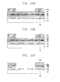
- FIGS. 10A through 10H are sequential sectional views illustrating a method for fabricating an OLED display device according to a fifth embodiment of the present invention.
- a gate line including a first gate electrode and a storage electrode including a second gate electrode may be formed on a substrate 510 made of an insulating material such as transparent glass, plastic, or the like.
- a gate insulating layer made of silicon nitride (SiNx), silicon oxide (SiO 2 ), or the like, may be formed on the gate line including the first gate electrode and the storage electrode including the second electrode.
- a first active layer and a second active layer, made of semiconductor, may be formed on the gate insulating layer.
- the first active layer and the second active layer may be positioned on the first gate electrode and the second gate electrode, respectively.
- a data line, a driving voltage line, a first source/drain electrode, and a second source/drain electrode may be formed on an upper portion of the first active layer and the second active layer.
- a predetermined passivation layer may be formed on the substrate 510 on which the data line, the driving voltage line, the first source/drain electrode, and the second source/drain electrode have been formed.
- a pixel electrode 520 and a connecting electrode may be formed on the substrate 510 with the passivation film formed thereon.
- the pixel electrode 520 and the connecting electrode may be made of a transparent conductive material such as indium tin oxide (ITO) or a reflective conductive material such as aluminum, silver, or an alloy thereof.
- the pixel electrode 520 as an anode may be electrically connected to the second drain electrode through a second contact hole, and the connecting electrode may electrically connect the first drain electrode and the second gate electrode through a first contact hole and a third contact hole.
- a partition may be formed on the substrate 510 with the pixel electrode 520 formed thereon.
- the partition may encompass the edges of the pixel electrode 520, like a bank, to define an opening, and may be made of an organic insulating material or an inorganic insulating material.
- An organic compound layer may be formed on the substrate 510.
- the organic compound layer may have a multilayer structure including an auxiliary layer in order to enhance luminous efficiency of a light emitting layer that emits light, besides the light emitting layer.
- the auxiliary layer may include an electron transport layer and a hole transport layer for balancing electrons and holes and an electron injection layer and a hole injection layer for strengthening injection of electrons and holes.
- a thin film 531 for a first hole injection layer, a thin film 541 for a first hole transport layer, a first organic film 551, a thin film 561 for a first electron transport layer, and a first conductive film 581 are sequentially deposited on the substrate 510 with the pixel electrode 520 formed thereon.
- the thin film 561 for a first electron transport layer may include a thin film for a first electron injection layer
- the first conductive film 581 may be made of a reflective conductive material including calcium (Ca), barium (Ba), magnesium (Mg), aluminum (Al), silver (Ag), or the like, or a transparent conductive material such as ITO, IZO, or the like.
- a photosensitive resin is coated on the entire surface of the substrate 510, on which the thin film 531 for a first hole injection layer, the thin film 541 for a first hole transport layer, the first organic film 551, the thin film 561 for a first electron transport layer, and the first conductive film 581 have been deposited, to form a first photosensitive resin layer 591.
- UV rays are selectively irradiated to the first photosensitive resin layer 591 through a certain mask M.
- a first photosensitive resin pattern 590a made of the photosensitive resin remains only at a position where a first light emitting layer is to be formed as shown in FIG. 10D .
- the first photosensitive resin pattern 590a may be patterned to have at least the same width as that of the underlying pixel electrode 520 in consideration of an alignment error of the mask M and other processing errors.
- a first common electrode 580a formed of the first conductive film is formed at a position where the first light emitting layer is to be formed.
- the etching may include wet etching as well as dry etching.
- a remnant of the first photosensitive resin pattern is removed through ashing, stripping, or the like, and here, as partial regions of the thin film for a first hole injection layer, the thin film for a first hole transport layer, the first organic film, and the thin film for a first electron transport layer exposed thereunder are selectively removed by using the first common electrode 580a as a mask, a first hole injection layer 530a, a first hole transport layer 540a, a first light emitting layer 550a, and a first electron transport layer 560a, which are formed of the thin film for a first hole injection layer, the thin film for a first hole transport layer, the first organic film, and the thin film for a first electron transport layer, respectively, are formed (a first photo process).
- the first common electrode 580a is positioned as a barrier layer on an upper portion of the organic compound layer, namely, on the first electron transport layer 560a, the organic compound layer, in particular, the first electron transport layer 560a, can be prevented from being degraded during the photo process, thus preventing a degradation of the device.
- the first light emitting layer 550a may be a red light emitting layer, but the present invention is not limited thereto and the first light emitting layer 550a may be a green or blue light emitting layer.
- a second hole injection layer 530b, a second hole transport layer 540b, a second light emitting layer 550b, a second electron transport layer 560b, and a second common electrode 580b which are formed of a thin film for a second hole injection layer, a thin film for a second hole transport layer, a second organic film, a thin film for a second electron transport layer, and a second conductive film, respectively, are formed on the substrate 510 through a second photo process which is substantially the same as the first photo process as mentioned above.
- the second conductive film may be made of a reflective conductive material including calcium (Ca), barium (Ba), magnesium (Mg), aluminum (Al), silver (Ag), or the like, or a transparent conductive material such as ITO, IZO, or the like.
- a reflective conductive material including calcium (Ca), barium (Ba), magnesium (Mg), aluminum (Al), silver (Ag), or the like, or a transparent conductive material such as ITO, IZO, or the like.
- the second light emitting layer 550b may be a green light emitting layer.
- the present invention is not limited thereto and when the first light emitting layer 550a is a red light emitting layer, the second light emitting layer 550b may be a blue light emitting layer, other than a green light emitting layer.
- a third hole injection layer 530c, a third hole transport layer 540c, a third light emitting layer 550c, a third electron transport layer 560c, and a third common electrode 580c which are formed of a thin film for a third hole injection layer, a thin film for a third hole transport layer, a third organic film, a thin film for a third electron transport layer, and a third conductive film, respectively, are formed on the substrate 510 through a third photo process which is substantially the same as the first and second photo processes as mentioned above.
- the third conductive film may be made of a reflective conductive material including calcium (Ca), barium (Ba), magnesium (Mg), aluminum (Al), silver (Ag), or the like, or a transparent conductive material such as ITO, IZO, or the like.
- a reflective conductive material including calcium (Ca), barium (Ba), magnesium (Mg), aluminum (Al), silver (Ag), or the like, or a transparent conductive material such as ITO, IZO, or the like.
- the third light emitting layer 550c may be a blue light emitting layer.
- the third light emitting layer 550c may be a green light emitting layer.
- the present invention is not limited thereto and the first light emitting layer 550a, the second light emitting layer 550b, and the third light emitting layer 550c may be configured as red, green, and blue light emitting layers irrespective of order.
- the first gate electrode connected to the gate line and the first source electrode and the first drain electrode connected to the data line may constitute a first switching thin film transistor (TFT) along with the first active layer.
- the second gate electrode connected to the first drain electrode, the second source electrode connected to the driving voltage line, and the second drain electrode connected to the pixel electrode 520 may constitute a driving TFT along with the second active layer.
- the pixel electrode 520, the light emitting layers 550a, 550b, and 550c, and the common electrodes 580a, 580b, and 580c may constitute an OLED, and the mutually overlapping storage electrode and driving voltage line may constitute a storage capacitor.
- the organic compound layer and the common electrodes are patterned at intervals between neighboring pixels, but the present invention is not limited thereto.
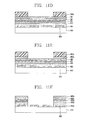
- FIGS. 11A through 11H are sequential sectional views illustrating a method for fabricating an OLED display device according to a sixth embodiment of the present invention, in which a method for fabricating an OLED diode with respect to some pixels is taken as an example.
- the OLED display device has the same configuration as that of the fifth embodiment of the present invention, except that the organic compound layer and the common electrodes are patterned to be in contact with each other between neighboring pixels.
- a gate line including a first gate electrode and a storage electrode including a second gate electrode may be formed on a substrate 610 made of an insulating material such as transparent glass, plastic, or the like.
- a gate insulating layer made of silicon nitride (SiNx), silicon oxide (SiO 2 ), or the like, may be formed on the gate line including the first gate electrode and the storage electrode including the second electrode.
- a first active layer and a second active layer, made of semiconductor, may be formed on the gate insulating layer.
- the first active layer and the second active layer may be positioned on the first gate electrode and the second gate electrode, respectively.
- a data line, a driving voltage line, a first source/drain electrode, and a second source/drain electrode may be formed on an upper portion of the first active layer and the second active layer.
- a predetermined passivation layer may be formed on the substrate 610 on which the data line, the driving voltage line, the first source/drain electrode, and the second source/drain electrode have been formed.
- a pixel electrode 620 and a connecting electrode may be formed on the substrate 610 with the passivation film formed thereon.
- the pixel electrode 620 and the connecting electrode may be made of a transparent conductive material such as indium tin oxide (ITO) or a reflective conductive material such as aluminum, silver, or an alloy thereof.
- the pixel electrode 620 as an anode may be electrically connected to the second drain electrode through a second contact hole, and the connecting electrode may electrically connect the first drain electrode and the second gate electrode through a first contact hole and a third contact hole.
- a partition may be formed on the substrate 610 with the pixel electrode 620 formed thereon.
- the partition may encompass the edges of the pixel electrode 620, like a bank, to define an opening, and may be made of an organic insulating material or an inorganic insulating material.
- An organic compound layer may be formed on the substrate 610.
- the organic compound layer may have a multilayer structure including an auxiliary layer in order to enhance luminous efficiency of a light emitting layer that emits light, besides the light emitting layer.
- the auxiliary layer may include an electron transport layer and a hole transport layer for balancing electrons and holes and an electron injection layer and a hole injection layer for strengthening injection of electrons and holes.
- a thin film 631 for a first hole injection layer, a thin film 641 for a first hole transport layer, a first organic film 651, a thin film 661 for a first electron transport layer, and a first conductive film 681 are sequentially deposited on the substrate 610 with the pixel electrode 620 formed thereon.
- the thin film 661 for a first electron transport layer may include a thin film for a first electron injection layer
- the first conductive film 681 may be made of a reflective conductive material including calcium (Ca), barium (Ba), magnesium (Mg), aluminum (Al), silver (Ag), or the like, or a transparent conductive material such as ITO, IZO, or the like.
- a photosensitive resin is coated on the entire surface of the substrate 610, on which the thin film 631 for a first hole injection layer, the thin film 641 for a first hole transport layer, the first organic film 651, the thin film 661 for a first electron transport layer, and the first conductive film 681 have been deposited, to form a first photosensitive resin layer 691.
- UV rays are selectively irradiated to the first photosensitive resin layer 691 through a certain mask M.
- a first photosensitive resin pattern 690a made of the photosensitive resin remains only at a position where a first light emitting layer is to be formed as shown in FIG. 11D .
- the first photosensitive resin pattern 690a may be patterned such that the organic compound layer and a common electrode are patterned to be in contact with each other between neighboring pixels.
- a first common electrode 680a formed of the first conductive film is formed at a position where the first light emitting layer is to be formed.
- the etching may include wet etching as well as dry etching.
- a remnant of the first photosensitive resin pattern is removed through ashing, stripping, or the like, and here, as partial regions of the thin film for a first hole injection layer, the thin film for a first hole transport layer, the first organic film, and the thin film for a first electron transport layer exposed thereunder are selectively removed by using the first common electrode 680a as a mask, a first hole injection layer 630a, a first hole transport layer 640a, a first light emitting layer 650a, and a first electron transport layer 660a, which are formed of the thin film for a first hole injection layer, the thin film for a first hole transport layer, the first organic film, and the thin film for a first electron transport layer, respectively, are formed (a first photo process).
- the first common electrode 680a is positioned as a barrier layer on an upper portion of the organic compound layer, namely, on the first electron transport layer 660a, the organic compound layer, in particular, the first electron transport layer 660a, can be prevented from being degraded during the photo process, thus preventing a degradation of the device.
- the first light emitting layer 650a may be a red light emitting layer, but the present invention is not limited thereto and the first light emitting layer 650a may be a green or blue light emitting layer.
- a second hole injection layer 630b, a second hole transport layer 640b, a second light emitting layer 650b, a second electron transport layer 660b, and a second common electrode 680b which are formed of a thin film for a second hole injection layer, a thin film for a second hole transport layer, a second organic film, a thin film for a second electron transport layer, and a second conductive film, respectively, are formed on the substrate 610 through a second photo process which is substantially the same as the first photo process as mentioned above.
- the second conductive film may be made of a reflective conductive material including calcium (Ca), barium (Ba), magnesium (Mg), aluminum (Al), silver (Ag), or the like, or a transparent conductive material such as ITO, IZO, or the like.
- a reflective conductive material including calcium (Ca), barium (Ba), magnesium (Mg), aluminum (Al), silver (Ag), or the like, or a transparent conductive material such as ITO, IZO, or the like.
- the second light emitting layer 650b may be a green light emitting layer.
- the present invention is not limited thereto and when the first light emitting layer 650a is a red light emitting layer, the second light emitting layer 650b may be a blue light emitting layer, other than a green light emitting layer.
- a third hole injection layer 630c, a third hole transport layer 640c, a third light emitting layer 650c, a third electron transport layer 660c, and a third common electrode 680c which are formed of a thin film for a third hole injection layer, a thin film for a third hole transport layer, a third organic film, a thin film for a third electron transport layer, and a third conductive film, respectively, are formed on the substrate 610 through a third photo process which is substantially the same as the first and second photo processes as mentioned above.
- the third conductive film may be made of a reflective conductive material including calcium (Ca), barium (Ba), magnesium (Mg), aluminum (Al), silver (Ag), or the like, or a transparent conductive material such as ITO, IZO, or the like.
- a reflective conductive material including calcium (Ca), barium (Ba), magnesium (Mg), aluminum (Al), silver (Ag), or the like, or a transparent conductive material such as ITO, IZO, or the like.
- the third light emitting layer 650c may be a blue light emitting layer.
- the third light emitting layer 650c may be a green light emitting layer.
- the present invention is not limited thereto and the first light emitting layer 650a, the second light emitting layer 650b, and the third light emitting layer 650c may be configured as red, green, and blue light emitting layers irrespective of order.
- the first gate electrode connected to the gate line and the first source electrode and the first drain electrode connected to the data line may constitute a first switching thin film transistor (TFT) along with the first active layer.
- the second gate electrode connected to the first drain electrode, the second source electrode connected to the driving voltage line, and the second drain electrode connected to the pixel electrode 620 may constitute a driving TFT along with the second active layer.
- the pixel electrode 620, the light emitting layers 650a, 650b, and 650c, and the common electrodes 680a, 680b, and 680c may constitute an OLED, and the mutually overlapping storage electrode and driving voltage line may constitute a storage capacitor.
Landscapes
- Physics & Mathematics (AREA)
- Optics & Photonics (AREA)
- Engineering & Computer Science (AREA)
- Manufacturing & Machinery (AREA)
- Electroluminescent Light Sources (AREA)
Abstract
Description
- The present invention relates to organic light emitting diode (OLED) display device and a method of fabricating the same and, more particularly, to an OLED display device in which OLED pixels are patterned through a photolithography process, and a method of fabricating the same.
- Recently, as interest in information displays has been on the rise and demand for the use of portable information media has been increased, lightweight flat panel displays (FPDs) substituting cathode ray tubes (CRTs) as existing display devices have been actively researched and commercialized.
- In the FPD fields, a liquid crystal display (LCD) device, which is lighter and consumes less power, has been spotlighted; however, since an LCD device is a light receiving device, rather than a light emitting device, having shortcomings of brightness, contrast ratio, and a viewing angle, and the like, so a development of a new display device that may overcome such drawbacks has been actively made.
- An LED display device, one of new display devices, is a self-luminous type device, which thus is excellent in a viewing angle and contrast ratio, is lighter and thinner because it does not need a backlight, and is advantageous in terms of power consumption, relative to an LCD device. In addition, an OLED display device can be driven by a DC and at a low voltage, has a fast response speed, and is especially advantageous in terms of fabrication costs.
- Unlike an LCD device or a plasma display panel (PDP), deposition and encapsulation are the whole of a fabrication process of an OLED display device, so the fabrication process is very simple. Also, when the OLED display device is driven according to an active matrix scheme in which each pixel has a thin film transistor (TFT) as a switching element, the same luminance can be obtained although a low current is applied, so, advantageously, the OLED display device consumes low power, has a high pitch (or high definition or high resolution), and can be increased in size.
- Hereinafter, a basic structure and operational characteristics of an OLED display device will be described in detail with reference to the accompanying drawings.
-
FIG. 1 is a diagram illustrating a light emission principle of a general OLED display device. - As shown in
FIG. 1 , a general OLED display device includes an OLED. The OLED includesorganic compound layers anode 18 as a pixel electrode and acathode 28 as a common electrode. - Here, the
organic compound layers hole injection layer 30a, ahole transport layer 30b, anemission layer 30c, anelectron transport layer 30d, and anelectron injection layer 30e. - When a driving voltage is applied to the
anode 18 and thecathode 28, holes which have passed through thehole transport layer 30b and electrons which have passed through theelectron transport layer 30e move to thelight emission layer 30c to form excitons, and as a result, thelight emission layer 30c emits visible light. - In the OLED display device, the pixels each having the OLED having the foregoing structure are arranged in a matrix form and selectively controlled by a data voltage and a scan voltage to display an image.
- The OLED display device is divided into a passive matrix type OLED display device and an active matrix type display device using TFTs as switching elements. Among them, in the active matrix type OLED display device, TFTs as active elements are selectively turned on to select pixels and emitting of pixels is maintained by a voltage maintained in a storage capacitor.
-
FIG. 2 is an equivalent circuit diagram of a pixel in a general OLED display device. Namely,FIG. 2 illustrates an example of an equivalent circuit diagram of a pixel having a general 2T1C (including two transistors and one capacitor) in an active matrix type OLED display device. - Referring to
FIG. 2 , a pixel of an active matrix type OLED display device includes an OLED, a data line DL and a gate line GL crossing each other, a switching TFT SW, a driving TFT DR, and a storage capacitor Cst. - Here, the switching TFT SW is turned on in response to a scan pulse from the gate line GL to conduct a current path between a source electrode and a drain electrode thereof. During an ON-time period of the switching TFT SW, a data voltage from the data line DL is applied to a gate electrode of the driving TFT DR and the storage capacitor Cst by way of the source electrode and drain electrode of the switching TFT SW.
- Here, the driving TFT DR controls a current flowing in the OLED according to the data voltage applied to the gate electrode thereof. The storage capacitor Cst stores a voltage between the data voltage and a low potential power source voltage VSS and uniformly maintains it during one frame period.
- In order to form the several organic compound layers constituting the OLED display device, a vacuum evaporation method is largely used.
- Here, in order to use the vacuum evaporation method, a mask (or a shadow mask) or a fine metal mask (FMM) having a plurality of openings corresponding to a plurality of pixel regions is used. However, this method has a limitation in that it is not easy to cope with a fine pitch of patterns for increasing a size of a substrate and implementing a high resolution display
- Namely, FMM is fabricated by forming holes as a pattern intended for deposition on a thin metal plate and stretching the same. Thus, there is a limitation in forming a pattern having a small size, making it difficult to reduce the size of an OLED. Also, when a fine metal mask is increased in size in order to increase a size of a panel, warpage occurs due to the characteristics of the fine metal mask, distort the pattern to degrade a production yield.
- An aspect of the present invention provides an organic light emitting diode (OLED) display device in which OLED pixels are patterned through a photolithography process, thus being available for large area patterning and obtaining a high pitch (or high definition or high resolution), and a method for fabricating the same.
- Another aspect of the present invention provides an OLED display device in which a light emitting layer is protected during a patterning process through photolithography, and a method for fabricating the same.
- Another aspect of the present invention provides an OLED display device capable of simplifying a process and increasing efficiency, and a method for fabricating the same.
- According to an aspect of the present invention, there is provided an organic light emitting diode (OLED) display device including: a first electrode formed on a substrate; a hole injection layer and a hole transport layer formed on the substrate with the first electrode formed thereon; a first light emitting layer formed of a first organic film on the substrate with the hole injection layer and the hole transport layer formed thereon; a second light emitting layer formed of a second organic film on the substrate with the first light emitting layer formed thereon; a third light emitting layer formed by depositing a third organic film on the entire surface of the substrate with the first light emitting layer and the second light emitting layer formed thereon; and an electron injection layer and a second electrode formed on the third light emitting layer.
- The third light emitting layer may be formed on upper portions of the first light emitting layer and the second light emitting layer as well as between the first light emitting layer and the second light emitting layer.
- According to another aspect of the present invention, there is provided an organic light emitting diode (OLED) display device including: a first electrode formed on a substrate; a first hole injection layer, a first hole transport layer, a first light emitting layer, a first electron transport layer, and a first buffer layer laminated on the substrate; a second hole injection layer, a second hole transport layer, a second light emitting layer, a second electron transport layer, and a second buffer layer laminated on the substrate; a third hole injection layer, a third hole transport layer, a third light emitting layer, a third electron transport layer, and a third buffer layer laminated on the substrate; and a second electrode formed on the first, second, and third buffer layers, wherein the first, second, and third buffer layers are made of a metal oxide.
- The first, second, and third buffer layers may be made of a 1-2 Group and 12-16 Group metal oxide or 3-12 Group transition metal oxide.
- According to another aspect of the present invention, there is provided a method for fabricating an organic light emitting diode (OLED) display device, including: forming a first electrode on a substrate; forming a first light emitting layer formed of a first organic film on the substrate through a first photo process; forming a second light emitting layer formed of a second organic film on the substrate through a second photo process; depositing a third organic film on first and second photosensitive resin patterns remaining after being used during the first and second photo processes; removing the third organic film deposited on upper portions of the first and second photosensitive resin patterns together with the first and second photosensitive resin patterns through a lift-off process to form a third light emitting layer; and forming a second electrode on the first, second, and third light emitting layers.
- According to another aspect of the present invention, there is provided a method for fabricating an organic light emitting diode (OLED) display device, including: (a) forming a first electrode on a substrate; (b) applying a photosensitive resin to the entire surface of the substrate to form a first photosensitive resin layer; (c) selectively exposing and developing the first photosensitive resin layer to form a first photosensitive resin pattern made of the photosensitive resin at a position other than a position where a first light emitting layer is to be formed; (d) depositing a first organic film on the first photosensitive resin pattern in a state in which the first photosensitive resin pattern remains; (e) removing the first organic film deposited on an upper portion of the first photosensitive resin pattern together with the first photosensitive resin pattern through a lift-off process to form a first light emitting layer formed of the first organic film on the substrate; (f) forming a second light emitting layer formed of a second organic film on the substrate through the same processes as (b) to (e); (g) depositing a third organic film on the entire surface of the substrate with the first light emitting layer and the second light emitting layer formed thereon; and (h) forming a second electrode on the substrate.
- The third light emitting layer may be formed between the first light emitting layer and the second light emitting layer.
- The third light emitting layer may be formed on upper portions of the first light emitting layer and the second light emitting layer as well as between the first light emitting layer and the second light emitting layer.
- After a hole injection layer and a hole transport layer are formed on the substrate with the first electrode formed thereon, the first light emitting layer may be formed thereon.
- The first light emitting layer may be formed as any one of red, green, and blue light emitting layers.
- The second light emitting layer may be formed as another one of the red, green, and blue light emitting layers.
- The third light emitting layer may be formed as the other remaining one of the red, green, and blue light emitting layers.
- After an electron transport layer and an electron injection layer are formed on the substrate with the first, second, and third light emitting layers formed thereon, the second electrode may be formed thereon.
- According to another aspect of the present invention, there is provided a method for fabricating an organic light emitting diode (OLED) display device, including: forming a first electrode on a substrate; forming a first hole injection layer, a first hole transport layer, a first light emitting layer, a first electron transport layer, and a first buffer layer in a laminated manner on the substrate through a first photo process; forming a second hole injection layer, a second hole transport layer, a second light emitting layer, a second electron transport layer, and a second buffer layer in a laminated manner on the substrate through a first photo process; forming a third hole injection layer, a third hole transport layer, a third light emitting layer, a third electron transport layer, and a third buffer layer in a laminated manner on the substrate through a first photo process; and forming a second electrode on the first, second, and third buffer layers, wherein the first, second, and third buffer layers are made of a metal oxide.
- According to another aspect of the present invention, there is provided a method for fabricating an organic light emitting diode (OLED) display device, including: (a) forming a first electrode on a substrate; (b) applying a photosensitive resin to the entire surface of the substrate to form a first photosensitive resin layer; (c) selectively exposing and developing the first photosensitive resin layer to form a first photosensitive resin pattern made of the photosensitive resin at a position other than a position where a first light emitting layer is to be formed; (d) depositing a thin film for a first hole injection layer, a thin film for a first hole transport layer, a first organic film, a thin film for a first electron transport layer, and a thin film for a first buffer layer in a state in which the first photosensitive resin pattern remains; (e) removing the thin film for a first hole injection layer, the thin film for a first hole transport layer, the first organic film, the thin film for a first electron transport layer, and the thin film for a first buffer layer deposited on an upper portion of the first photosensitive resin pattern together with the first photosensitive resin pattern through a lift-off process to form a first hole injection layer, a first hole transport layer, a first light emitting layer, a first electron transport layer, and a first buffer layer, which are formed of thin film for a first hole injection layer, the thin film for a first hole transport layer, the first organic film, the thin film for a first electron transport layer, and the thin film for a first buffer layer, respectively, on the substrate; (f) forming a second hole injection layer, a second hole transport layer, a second light emitting layer, a second electron transport layer, and a second buffer layer through the same processes as (b) to (e); (g) forming a third hole injection layer, a third hole transport layer, a third light emitting layer, a third electron transport layer, and a third buffer layer through the same processes as (b) to (e); and (h) forming a second electrode on the first, second, and third buffer layers, wherein the first, second, and third buffer layers are made of a metal oxide.
- The forming of the first hole injection layer, the first hole transport layer, the first light emitting layer, the first electron transport layer, and the first buffer layer may include: depositing a thin film for a first hole injection layer, a thin film for a first hole transport layer, a first organic film, a thin film for a first electron transport layer, and a thin film for a first buffer layer on the substrate; applying a photosensitive resin to the entire surface of the substrate with the thin film for a first hole injection layer, the thin film for a first hole transport layer, the first organic film, the thin film for a first electron transport layer, and the thin film for a first buffer layer deposited thereon to form a first photosensitive resin layer; exposing and developing the first photosensitive resin layer to from a first photosensitive resin pattern made of the photosensitive resin at a position where a first light emitting is to be formed; and selectively etching the thin film for a first hole injection layer, the thin film for a first hole transport layer, the first organic film, the thin film for a first electron transport layer, and the thin film for a first buffer layer by using the first photosensitive resin pattern as a mask to form the first hole injection layer, the first hole transport layer, the first light emitting layer, the first electron transport layer, and the first buffer layer, which are formed of thin film for a first hole injection layer, the thin film for a first hole transport layer, the first organic film, the thin film for a first electron transport layer, and the thin film for a first buffer layer, respectively, on the substrate.
- The forming of the second hole injection layer, the second hole transport layer, the second light emitting layer, the second electron transport layer, and the second buffer layer may include: depositing a thin film for a second hole injection layer, a thin film for a second hole transport layer, a second organic film, a thin film for a second electron transport layer, and a thin film for a second buffer layer on the substrate; applying a photosensitive resin to the entire surface of the substrate with the thin film for a second hole injection layer, the thin film for a second hole transport layer, the second organic film, the thin film for a second electron transport layer, and the thin film for a second buffer layer deposited thereon to form a second photosensitive resin layer; exposing and developing the second photosensitive resin layer to from a second photosensitive resin pattern made of the photosensitive resin at a position where a second light emitting is to be formed; and selectively etching the thin film for a second hole injection layer, the thin film for a second hole transport layer, the second organic film, the thin film for a second electron transport layer, and the thin film for a second buffer layer by using the second photosensitive resin pattern as a mask to form the second hole injection layer, the second hole transport layer, the second light emitting layer, the second electron transport layer, and the second buffer layer, which are formed of thin film for a second hole injection layer, the thin film for a second hole transport layer, the second organic film, the thin film for a second electron transport layer, and the thin film for a second buffer layer, respectively, on the substrate.
- The forming of the third hole injection layer, the third hole transport layer, the third light emitting layer, the third electron transport layer, and the third buffer layer may include: depositing a thin film for a third hole injection layer, a thin film for a third hole transport layer, a third organic film, a thin film for a third electron transport layer, and a thin film for a third buffer layer on the substrate; applying a photosensitive resin to the entire surface of the substrate with the thin film for a third hole injection layer, the thin film for a third hole transport layer, the third organic film, the thin film for a third electron transport layer, and the thin film for a third buffer layer deposited thereon to form a third photosensitive resin layer; exposing and developing the third photosensitive resin layer to from a third photosensitive resin pattern made of the photosensitive resin at a position where a third light emitting is to be formed; and selectively etching the thin film for a third hole injection layer, the thin film for a third hole transport layer, the third organic film, the thin film for a third electron transport layer, and the thin film for a third buffer layer by using the third photosensitive resin pattern as a mask to form the third hole injection layer, the third hole transport layer, the third light emitting layer, the third electron transport layer, and the third buffer layer, which are formed of thin film for a third hole injection layer, the thin film for a third hole transport layer, the third organic film, the thin film for a third electron transport layer, and the thin film for a third buffer layer, respectively, on the substrate.
- The first, second, and third buffer layers may be made of a 1-2 Group and 12-16 Group metal oxide or 3-12 Group transition metal oxide.
- According to another aspect of the present invention, there is provided a method for fabricating an organic light emitting diode (OLED) display device, including: (a) forming a fourth electrode on a substrate; (b) forming a first organic film and a first conductive film on the substrate with the fourth electrode formed thereon; (c) applying a photosensitive resin to the entire surface of the substrate with the first conductive film formed thereon to form a first photosensitive resin layer; (d) selectively exposing and developing the first photosensitive resin layer to form a first photosensitive resin pattern made of the photosensitive resin at a position at which a first light emitting is to be formed; (e) selectively removing the first conductive film by using the first photosensitive resin pattern as a mask to form a first electrode; (f) removing the first photosensitive resin pattern and selectively removing the underlying exposed first organic film by using the first electrode as a mask to form a first light emitting layer formed of the first organic film; (g) forming a second light emitting layer and a second electrode on the substrate through the same processes as (b) to (f); and (h) forming a third light emitting layer and a third electrode on the substrate through the same processes as (b) to (f).
- After a thin film for a first hole injection layer and a thin film for a first hole transport layer are formed on the substrate with the fourth electrode formed thereon, the first organic film may be formed, and after a thin film for a first electron transport layer is formed, the first conductive film may be formed.
- As described above, in the case of the OLED display device and the method for fabricating the same according to embodiments of the present invention, since OLED pixels are patterned through a photolithography process, a large area patterning can be performed and a fine pitch can be obtained, and an organic compound layer can be protected by forming a buffer layer of a metal oxide on an upper portion of the organic compound layer or patterning the organic compound layer by using a cathode as a mask, improving device efficiency. Here, patterning through a photolithography process can be performed through a solution process, and since a light emitting layer is protected during a patterning process, a driving voltage and power consumption of the device can be reduced and efficiency can be enhanced.
- Also, in the case of the OLED display device and the method for fabricating the same according to embodiments of the present invention, among red, green, and blue pixels, two pixels are patterned through a lift-off process and the other remaining one is deposited to be formed without patterning, the process can be simplified and efficiency can be increased.
- The foregoing and other objects, features, aspects and advantages of the present invention will become more apparent from the following detailed description of the present invention when taken in conjunction with the accompanying drawings.
-
-
FIG. 1 is a diagram illustrating a light emission principle of a general organic light emitting diode (OLED) display device. -
FIG. 2 is an equivalent circuit diagram of a pixel in a general OLED display device. -
FIGS. 3A through 3L are sequential sectional views illustrating a method for fabricating an OLED display device according to a first embodiment of the present invention. -
FIGS. 4A through 4H are sequential sectional views illustrating a method for fabricating an OLED display device according to a second embodiment of the present invention. -
FIGS. 5A through 5G are sequential sectional views illustrating a method for fabricating an OLED display device according to a third embodiment of the present invention. -
FIG. 6 is a graph showing a state in which a life span of a device is shortened after a photolithography process is performed. -
FIGS. 7A through 7K are sequential sectional views illustrating a method for fabricating an OLED display device according to a fourth embodiment of the present invention. -
FIG. 8 is a sectional view showing another example of an OLED display device fabricated according to the fourth embodiment of the present invention illustrated inFIGS. 7A through 7K . -
FIG. 9 is a sectional view showing another example of an OLED display device fabricated according to the fourth embodiment of the present invention illustrated inFIGS. 7A through 7K . -
FIGS. 10A through 10H are sequential sectional views illustrating a method for fabricating an OLED display device according to a fifth embodiment of the present invention. -
FIGS. 11A through 11H are sequential sectional views illustrating a method for fabricating an OLED display device according to a sixth embodiment of the present invention. - Hereinafter, an organic light emitting diode (OLED) display device and a method for fabricating the same according to embodiments of the present invention will be described in detail with reference to the accompanying drawings such that they can be easily implemented by a person skilled in the art to which the present invention pertains. The present invention may be implemented in various forms without being limited to the embodiments described herein. Patterning of a large area with respect to an organic compound layer of an OLED display device cannot be handled by an existing method using a fine metal mask due to sagging of a substrate and a mask, so various large area patterning methods have been researched. Among them, the present invention proposes a patterning method through a photolithography process (referred to as a 'photo process', hereinafter), and here, the photo process is advantageous in that it is available for large area patterning and obtaining a fine pitch, and available for an application of a solution process.
-
FIGS. 3A through 3L are sequential sectional views illustrating a method for fabricating an OLED display device according to a first embodiment of the present invention, in which a method for fabricating an OLED diode with respect to some pixels is taken as an example. - Here, a method for fabricating an OLED with respect to a pixel including 2T1C (two transistors and one capacitor) is taken as an example for the description purpose, but the present invention is not limited thereto.
- First, although not shown, in an OLED display device according to a first embodiment of the present invention, a gate line including a first gate electrode and a storage electrode including a second gate electrode may be formed on a
substrate 110 made of an insulating material such as transparent glass, plastic, or the like. - A gate insulating layer made of silicon nitride (SiNx), silicon oxide (SiO2), or the like, may be formed on the gate line including the first gate electrode and the storage electrode including the second electrode.
- A first active layer and a second active layer, made of semiconductor, may be formed on the gate insulating layer. The first active layer and the second active layer may be positioned on the first gate electrode and the second gate electrode, respectively.
- A data line, a driving voltage line, a first source/drain electrode, and a second source/drain electrode may be formed on an upper portion of the first active layer and the second active layer.
- A predetermined passivation layer may be formed on the
substrate 110 on which the data line, the driving voltage line, the first source/drain electrode, and the second source/drain electrode have been formed. - As shown in
FIG. 3A , apixel electrode 120 and a connecting electrode (not shown) may be formed on thesubstrate 110 with the passivation film formed thereon. Thepixel electrode 120 and the connecting electrode may be made of a transparent conductive material such as indium tin oxide (ITO) or a reflective conductive material such as aluminum, silver, or an alloy thereof. - The
pixel electrode 120 as an anode may be electrically connected to the second drain electrode through a second contact hole, and the connecting electrode may electrically connect the first drain electrode and the second gate electrode through a first contact hole and a third contact hole. - A partition (not shown) may be formed on the
substrate 110 with thepixel electrode 120 formed thereon. Here, the partition may encompass the edges of thepixel electrode 120, like a bank, to define an opening, and may be made of an organic insulating material or an inorganic insulating material. - An organic compound layer may be formed on the
substrate 110. - Here, the organic compound layer may have a multilayer structure including an auxiliary layer in order to enhance luminous efficiency of a light emitting layer that emits light, besides the light emitting layer. The auxiliary layer may include an electron transport layer and a hole transport layer for balancing electrons and holes and an electron injection layer and a hole injection layer for strengthening injection of electrons and holes.
- The organic compound layer may be formed through a photo process and a lift-off process, and to this end, as shown in
FIG. 3B , a firstorganic film 151 is deposited on thesubstrate 110. - Here, the first
organic film 151 may be deposited after the hole injection layer and the hole transport layer are formed on thesubstrate 110, and here, the firstorganic film 151 may be deposited to form a red, green, or blue light emitting layer. - The hole injection layer may facilitate injection of holes from the
pixel electrode 120, and the hole transport layer serves to allow holes to be transported to the light emitting layer. - Thereafter, as shown in
FIG. 3C , a photosensitive resin (or photoresist) is coated on the entire surface of thesubstrate 110 with the firstorganic film 151 deposited thereon, to form a firstphotosensitive resin layer 191. - Ultraviolet rays are selectively irradiated (exposure) to the first
photosensitive resin layer 191 through a certain mask (not shown). - Thereafter, when the first
photosensitive resin layer 191 exposed through the mask is developed, a firstphotosensitive resin pattern 190a made of the photosensitive resin remains only at a position where a first light emitting layer is to be formed as shown inFIG. 3D . - A photosensitive resin developing solution is used for the developing operation, and here, any developing solution may be used as long as it does not dissolve a material of the light emitting layer. For example, a generally used organic alkali-based developing solution may be used, or an inorganic alkali-based developing solution or an aqueous solution capable of developing resist may be used.
- Thereafter, as shown in
FIG. 3E , a partial region of the first organic film formed under the firstphotosensitive resin pattern 190a is selectively etched by using the firstphotosensitive resin pattern 190a as a mask, to form a firstlight emitting layer 150a formed of the first organic film on the substrate 110 (first photo process). - Here, for example, the first
light emitting layer 150a may be a red light emitting layer, and the etching may include wet etching as well as dry etching. However, the present invention is not limited thereto and the firstlight emitting layer 150a may be a red or blue light emitting layer. - Thereafter, as shown in
FIG. 3F , with the firstphotosensitive resin pattern 190a remaining, a secondorganic film 152 is deposited thereon. - A follow-up process is substantially the same as the first photo process for forming the first
light emitting layer 150a. Namely, as shown inFIG. 3G , a photosensitive resin is coated on the entire surface of thesubstrate 110 with the secondorganic film 152 formed thereon, to form a secondphotosensitive resin layer 192. - Thereafter, UV rays are selectively irradiated to the second
photosensitive resin layer 192 through a certain mask (not shown). - Thereafter, when the second
photosensitive resin layer 192 exposed through the mask is developed, a secondphotosensitive resin pattern 190b made of the photosensitive resin remains only at a position where a second light emitting layer is to be formed as shown inFIG. 3H . - Thereafter, as shown in
FIG. 3I , a partial region of the first organic film formed under the secondphotosensitive resin pattern 190b is selectively etched by using the secondphotosensitive resin pattern 190b as a mask, to form a secondlight emitting layer 150b formed of the second organic film on the substrate 110 (second photo process). - Here, for example, the second emitting
layer 150b may be a green light emitting layer, and the etching may include wet etching as well as dry etching. However, the present invention is not limited thereto and when the firstlight emitting layer 150a is a red light emitting layer, the secondlight emitting layer 150b may be a blue light emitting layer, other than a green light emitting layer. - Thereafter, as shown in
FIG. 3J , with the firstphotosensitive resin pattern 190a and the secondphotosensitive resin pattern 190b remaining, a thirdorganic film 153 is deposited thereon. - As a follow-up process, a lift-off process, rather than a photo process such as the first and second photo processes as described above, is used. Namely, as shown in
FIG. 3K , the first photosensitive resin pattern and the second photosensitive resin pattern are removed through a lift-off process, and here, the third organic film remaining on upper portions of the firstlight emitting layer 150a and the secondlight emitting layer 150b is removed along with the first photosensitive resin pattern and the second photosensitive resin pattern. - As a result, a third
light emitting layer 150c formed of the third organic film is formed between the firstlight emitting layer 150a and the secondlight emitting layer 150b. - Here, for example, when the first
light emitting layer 150a is a red light emitting layer and the secondlight emitting layer 150b is a green light emitting layer, the thirdlight emitting layer 150c may be a blue light emitting layer. Also, when the firstlight emitting layer 150a is a red light emitting layer and the secondlight emitting layer 150b is a blue light emitting layer, the thirdlight emitting layer 150c may be a green light emitting layer. However, the present invention is not limited thereto and the firstlight emitting layer 150a, the secondlight emitting layer 150b, and the thirdlight emitting layer 150c may be configured as red, green, and blue light emitting layers irrespective of order. - Thereafter, as shown in
FIG. 3L , acommon electrode 180 as a cathode may be formed on the firstlight emitting layer 150a, the secondlight emitting layer 150b, and the thirdlight emitting layer 150c. Here, the common electrode, which receives a common voltage, may be made of a reflective conductive material including calcium (Ca), barium (Ba), magnesium (Mg), aluminum (Al), silver (Ag), or the like, or a transparent conductive material such as ITO, IZO, or the like. - Here, the foregoing
common electrode 180 may be formed after the electron transport layer and the electron injection layer are formed on thesubstrate 110. - The electron injection layer facilitates injection of electrons from the
common electrode 180, and the electron transport layer serves to allow electrons to move to thelight emitting layers - In this manner, in the case of the first embodiment of the present invention, since a single photo process, namely, a single photosensitive resin coating, exposing, developing, and etching process (a total of four processes) may be omitted, and thus, the process can be simplified. Also, since OLED pixels are patterned through the photo process, large patterning can be performed and high pitch can be obtained, and in addition, a solution process can be performed.
- In the OLED display device configured as described above, the first gate electrode connected to the gate line and the first source electrode and the first drain electrode connected to the data line may constitute a first switching thin film transistor (TFT) along with the first active layer. Also, the second gate electrode connected to the first drain electrode, the second source electrode connected to the driving voltage line, and the second drain electrode connected to the
pixel electrode 120 may constitute a driving TFT along with the second active layer. - Also, the
pixel electrode 120, thelight emitting layers common electrode 180 may constitute an OLED, and the mutually overlapping storage electrode and driving voltage line may constitute a storage capacitor. - However, as mentioned above, when the organic compound layer is patterned through the photo process, the organic compound layer may be likely to be damaged by a photosensitive resin, a developing solution, and a strip solution, which may result in a degradation of efficiency and a life span.
- Thus, in case of second and third embodiments of the present invention, a buffer layer made of metal oxide is formed on an upper portion of the organic compound layer to protect the organic compound layer against a photo process. This will be described in detail with reference to the accompanying drawings.
-
FIGS. 4A through 4H are sequential sectional views illustrating a method for fabricating an OLED display device according to a second embodiment of the present invention, in which a method for fabricating an OLED diode with respect to some pixels is taken as an example. - Although not shown, as mentioned above, in an OLED display device according to a second embodiment of the present invention, a gate line including a first gate electrode and a storage electrode including a second gate electrode may be formed on a
substrate 210 made of an insulating material such as transparent glass, plastic, or the like. - A gate insulating layer made of silicon nitride (SiNx), silicon oxide (SiO2) or the like, may be formed on the gate line including the first gate electrode and the storage electrode including the second electrode.
- A first active layer and a second active layer, made of semiconductor, may be formed on the gate insulating layer. The first active layer and the second active layer may be positioned on the first gate electrode and the second gate electrode, respectively.
- A data line, a driving voltage line, a first source/drain electrode, and a second source/drain electrode may be formed on an upper portion of the first active layer and the second active layer.
- A predetermined passivation layer may be formed on the
substrate 210 on which the data line, the driving voltage line, the first source/drain electrode, and the second source/drain electrode have been formed. - As shown in
FIG. 4A , apixel electrode 220 and a connecting electrode (not shown) may be formed on thesubstrate 210 with the passivation film formed thereon. Thepixel electrode 220 and the connecting electrode may be made of a transparent conductive material such as indium tin oxide (ITO) or a reflective conductive material such as aluminum, silver, or an alloy thereof. - The
pixel electrode 220 as an anode may be electrically connected to the second drain electrode through a second contact hole, and the connecting electrode may electrically connect the first drain electrode and the second gate electrode through a first contact hole and a third contact hole. - A partition (not shown) may be formed on the
substrate 210 with thepixel electrode 220 formed thereon. Here, the partition may encompass the edges of thepixel electrode 220, like a bank, to define an opening, and may be made of an organic insulating material or an inorganic insulating material. An organic compound layer may be formed on thesubstrate 210. Here, the organic compound layer may have a multilayer structure including an auxiliary layer in order to enhance luminous efficiency of a light emitting layer that emits light, besides the light emitting layer. The auxiliary layer may include an electron transport layer and a hole transport layer for balancing electrons and holes and an electron injection layer and a hole injection layer for strengthening injection of electrons and holes. - Namely, as shown in
FIG. 4A , athin film 231 for a first hole injection layer, athin film 241 for a first hole transport layer, a firstorganic film 251, athin film 261 for a first electron transport layer, and athin film 271 for a first buffer layer are sequentially deposited on thesubstrate 210 with thepixel electrode 220 formed thereon. - Here, the
thin film 261 for a first electron transport layer may include a thin film for a first electron injection layer, and thethin film 271 for a first buffer layer may be made of a 1-2 Group and 12-16 Group metal oxide or 3-12 Group transition metal oxide. - Thereafter, as shown in
FIG. 4B , a photosensitive resin is coated on the entire surface of thesubstrate 210 on which thethin film 231 for a first hole injection layer, thethin film 241 for a first hole transport layer, the firstorganic film 251, thethin film 261 for a first electron transport layer, and thethin film 271 for a first buffer layer are deposited, in order to form a firstphotosensitive resin layer 291. - UV light is selectively irradiated to the first
photosensitive resin layer 291 through a certain mask (not shown). - Thereafter, when the first
photosensitive resin layer 291 exposed through the mask is developed, a firstphotosensitive resin pattern 290a made of the photosensitive resin remains only at a position where a first light emitting layer is to be formed as shown inFIG. 4C . - Thereafter, as shown in
FIG. 4D , partial regions of the thin film for a first hole injection layer, the thin film for a first hole transport layer, the first organic film, the thin film for a first electron transport layer, and the thin film for a first buffer layer formed under the firstphotosensitive resin pattern 290a are selectively etched by using the firstphotosensitive resin pattern 290a as a mask, in order to form a firsthole injection layer 230a, a firsthole transport layer 240a, a firstlight emitting layer 250a, a firstelectron transport layer 260a, and afirst buffer layer 270a formed of the thin film for a first hole injection layer, the thin film for a first hole transport layer, the first organic film, the thin film for a first electron transport layer, and the thin film for a first buffer layer, respectively, on the substrate 210 (first photo process). - In this manner, since the
first buffer layer 270a is positioned on the upper portion of the organic compound layer, namely, on the firstelectron transport layer 260a, the organic compound layer, in particular, the firstelectron transport layer 260a, is prevented from being degraded, thus preventing a degradation of the device. - Also, since the
first buffer layer 270a of metal oxide is applied, an energy barrier between the firstelectron transport layer 260a and the common electrode can be lowered, enhancing efficiency and a life span. - Here, for example, the first
light emitting layer 250a may be a red light emitting layer, and the etching may include wet etching, as well as dry etching. However, the present invention is not limited thereto and the firstlight emitting layer 250a may be a green or blue light emitting layer. - Thereafter, as shown in
FIG. 4E , the first photosensitive resin pattern is removed. - Thereafter, as shown in
FIG. 4F , a secondhole injection layer 230b, a secondhole transport layer 240b, a secondlight emitting layer 250b, a secondelectron transport layer 260b, and asecond buffer layer 270b, which are formed of a thin film for a second hole injection layer, a thin film for a second hole transport layer, a second organic film, a thin film for a second electron transport layer, and a thin film for a second buffer layer, respectively, are formed on thesubstrate 210 through a second photo process which is substantially the same as the first photo process as mentioned above. - Here, for example, the second
light emitting layer 250b may be a green light emitting layer. However, the present invention is not limited thereto and when the firstlight emitting layer 250a is a red light emitting layer, the secondlight emitting layer 250b may be a blue light emitting layer, other than a green light emitting layer. - Thereafter, as shown in
FIG. 4G , a thirdhole injection layer 230c, a thirdhole transport layer 240c, a thirdlight emitting layer 250c, a thirdelectron transport layer 260c, and athird buffer layer 270c, which are formed of a thin film for a third hole injection layer, a thin film for a third hole transport layer, a third organic film, a thin film for a third electron transport layer, and a thin film for a third buffer layer, respectively, are formed on thesubstrate 210 through a third photo process which is substantially the same as the first and second photo processes as mentioned above. - Here, for example, when the first
light emitting layer 250a is a red light emitting layer and the secondlight emitting layer 250b is a green light emitting layer, the thirdlight emitting layer 250c may be a blue light emitting layer. Also, when the firstlight emitting layer 250a is a red light emitting layer and the secondlight emitting layer 250b is a blue light emitting layer, the thirdlight emitting layer 250c may be a green light emitting layer. However, the present invention is not limited thereto and the firstlight emitting layer 250a, the secondlight emitting layer 250b, and the thirdlight emitting layer 250c may be configured as red, green, and blue light emitting layers irrespective of order. - Thereafter, as shown in
FIG. 4H ,common electrodes first buffer layer 270a, thesecond buffer layer 270b, and thethird buffer layer 270c. Here, thecommon electrodes - In the OLED display device configured as described above, the first gate electrode connected to the gate line and the first source electrode and the first drain electrode connected to the data line may constitute a first switching thin film transistor (TFT) along with the first active layer. Also, the second gate electrode connected to the first drain electrode, the second source electrode connected to the driving voltage line, and the second drain electrode connected to the
pixel electrode 220 may constitute a driving TFT along with the second active layer. - Also, the
pixel electrode 220, thelight emitting layers common electrodes -
FIGS. 5A through 5G are sequential sectional views illustrating a method for fabricating an OLED display device according to a third embodiment of the present invention, in which a method for fabricating an OLED diode with respect to some pixels is taken as an example. - Although not shown, as mentioned above, in an OLED display device according to a third embodiment of the present invention, a gate line including a first gate electrode and a storage electrode including a second gate electrode may be formed on a
substrate 310 made of an insulating material such as transparent glass, plastic, or the like. - A gate insulating layer made of silicon nitride (SiNx), silicon oxide (SiO2), or the like, may be formed on the gate line including the first gate electrode and the storage electrode including the second electrode.
- A first active layer and a second active layer, made of semiconductor, may be formed on the gate insulating layer. The first active layer and the second active layer may be positioned on the first gate electrode and the second gate electrode, respectively.
- A data line, a driving voltage line, a first source/drain electrode, and a second source/drain electrode may be formed on an upper portion of the first active layer and the second active layer.
- A predetermined passivation layer may be formed on the
substrate 310 on which the data line, the driving voltage line, the first source/drain electrode, and the second source/drain electrode have been formed. - As shown in
FIG. 5A , apixel electrode 320 and a connecting electrode (not shown) may be formed on thesubstrate 310 with the passivation film formed thereon. Thepixel electrode 320 and the connecting electrode may be made of a transparent conductive material such as indium tin oxide (ITO) or a reflective conductive material such as aluminum, silver, or an alloy thereof. - The
pixel electrode 320 as an anode may be electrically connected to the second drain electrode through a second contact hole, and the connecting electrode may electrically connect the first drain electrode and the second gate electrode through a first contact hole and a third contact hole. - A partition (not shown) may be formed on the
substrate 310 with thepixel electrode 320 formed thereon. Here, the partition may encompass the edges of thepixel electrode 320, like a bank, to define an opening, and may be made of an organic insulating material or an inorganic insulating material. - An organic compound layer may be formed on the
substrate 310. Here, in the case of the third embodiment of the present invention, unlike the second embodiment of the present invention as described above, the organic compound layer is formed through a lift-off process. - Namely, as shown in
FIG. 5A , a photosensitive resin is coated on the entire surface of thesubstrate 310 with thepixel electrode 320 formed thereon, to form a firstphotosensitive resin layer 391. - UV light is selectively irradiated to the first
photosensitive resin layer 391 through a certain mask (not shown). - Thereafter, when the first
photosensitive resin layer 391 exposed through the mask is developed, a firstphotosensitive resin pattern 390a made of the photosensitive resin remains only at a position other than a position where a first light emitting layer is to be formed as shown inFIG. 5B . - Thereafter, as shown in
FIG. 5C , with the firstphotosensitive resin pattern 390a remaining, athin film 331 for a first hole injection layer, athin film 341 for a first hole transport layer, a firstinorganic film 351, athin film 361 for a first electron transport layer, and athin film 371 for a first buffer layer are deposited on the firstphotosensitive resin pattern 390a. - Here, the
thin film 361 for a first electron transport layer may include a thin film for a first electron injection layer, and thethin film 371 for a first buffer layer may be made of a 1-2 Group and 12-16 Group metal oxide or 3-12 Group transition metal oxide. - Thereafter, as shown in
FIG. 5D , the firstphotosensitive resin pattern 390a is removed through a first lift-off process. Here, the thin film for a first hole injection layer, the thin film for a first hole transport layer, the first organic film, the thin film for the first electron transport layer, and the thin film for a first buffer layer remaining on the upper portion of the firstphotosensitive resin pattern 390a are also removed together with the firstphotosensitive resin pattern 390a. - As a result, a first hole injection layer 330, a first
hole transport layer 340a, a firstlight emitting layer 350a, a firstelectron transport layer 360a, and afirst buffer layer 370a, which are formed of the thin film for a first hole injection layer, the thin film for a first hole transport layer, the first organic film, the thin film for the first electron transport layer, and the thin film for a first buffer layer, respectively, are formed on thesubstrate 310. - Here, for example, the first
light emitting layer 350a may be a red light emitting layer. However, the present invention is not limited thereto and the firstlight emitting layer 350a may be a green or blue light emitting layer. - Thereafter, as shown in
FIG. 5E , a secondhole injection layer 330b, a secondhole transport layer 340b, a secondlight emitting layer 350b, a secondelectron transport layer 360b, and asecond buffer layer 370b, which are formed of a thin film for a second hole injection layer, a thin film for a second hole transport layer, a second organic film, a thin film for a second electron transport layer, and a thin film for a second buffer layer, respectively, are formed on thesubstrate 310 through a second lift-off process which is substantially the same as the first lift-off process as mentioned above. - Here, for example, the second
light emitting layer 350b may be a green light emitting layer. However, the present invention is not limited thereto and when the firstlight emitting layer 350a is a red light emitting layer, the secondlight emitting layer 350b may be a blue light emitting layer, other than a green light emitting layer. - Thereafter, as shown in
FIG. 5F , a thirdhole injection layer 330c, a thirdhole transport layer 340c, a thirdlight emitting layer 350c, a thirdelectron transport layer 360c, and athird buffer layer 370c, which are formed of a thin film for a third hole injection layer, a thin film for a third hole transport layer, a third organic film, a thin film for a third electron transport layer, and a thin film for a third buffer layer, respectively, are formed on thesubstrate 310 through a third lift-off process which is substantially the same as the first and second lift-off processes as mentioned above. - Here, for example, when the first
light emitting layer 350a is a red light emitting layer and the secondlight emitting layer 350b is a green light emitting layer, the thirdlight emitting layer 350c may be a blue light emitting layer. Also, when the firstlight emitting layer 350a is a red light emitting layer and the secondlight emitting layer 350b is a blue light emitting layer, the thirdlight emitting layer 350c may be a green light emitting layer. However, the present invention is not limited thereto and the firstlight emitting layer 350a, the secondlight emitting layer 350b, and the thirdlight emitting layer 350c may be configured as red, green, and blue light emitting layers irrespective of order. - Thereafter, as shown in
FIG. 5G ,common electrodes light emitting layer 350a, the secondlight emitting layer 350b, and the thirdlight emitting layer 350c. Here, thecommon electrodes - In the OLED display device configured as described above, the first gate electrode connected to the gate line and the first source electrode and the first drain electrode connected to the data line may constitute a first switching thin film transistor (TFT) along with the first active layer. Also, the second gate electrode connected to the first drain electrode, the second source electrode connected to the driving voltage line, and the second drain electrode connected to the
pixel electrode 320 may constitute a driving TFT along with the second active layer. - Also, the
pixel electrode 320, thelight emitting layers common electrodes - Meanwhile, organic substances whose efficiency and life span are rapidly reduced after the photo process is performed are included in the organic compound layer. For example, in the case of a blue light emitting layer, device efficiency tends to be reduced from about 5.3 cd/A to 2.0 cd/A after a photo process based on 1000 nit.
- For example, referring to
FIG. 6 , there is an organic substance whose life span is rapidly reduced after a photo process exists, which leads to a reduction in efficiency and life span of the LED display device. - Thus, in case of a fourth embodiment of the present invention, two pixels among red, green, and blue pixels are patterned through a lift-off process, while the other remaining one pixel is deposited to be formed without patterning, to thus simplify the process and increase efficiency. This will be described in detail with reference to the accompanying drawings.
-
FIGS. 7A through 7K are sequential sectional views illustrating a method for fabricating an OLED display device according to a fourth embodiment of the present invention, in which a method for fabricating an OLED diode with respect to some pixels is taken as an example. - Although not shown, as mentioned above, in an OLED display device according to a third embodiment of the present invention, a gate line including a first gate electrode and a storage electrode including a second gate electrode may be formed on a
substrate 410 made of an insulating material such as transparent glass, plastic, or the like. - A gate insulating layer made of silicon nitride (SiNx), silicon oxide (SiO2), or the like, may be formed on the gate line including the first gate electrode and the storage electrode including the second electrode.
- A first active layer and a second active layer, made of semiconductor, may be formed on the gate insulating layer. The first active layer and the second active layer may be positioned on the first gate electrode and the second gate electrode, respectively.
- A data line, a driving voltage line, a first source/drain electrode, and a second source/drain electrode may be formed on an upper portion of the first active layer and the second active layer.
- A predetermined passivation layer may be formed on the
substrate 410 on which the data line, the driving voltage line, the first source/drain electrode, and the second source/drain electrode have been formed. - As shown in
FIG. 7A , apixel electrode 420 and a connecting electrode (not shown) may be formed on thesubstrate 410 with the passivation film formed thereon. Thepixel electrode 420 and the connecting electrode may be made of a transparent conductive material such as indium tin oxide (ITO) or a reflective conductive material such as aluminum, silver, or an alloy thereof. - The
pixel electrode 420 as an anode may be electrically connected to the second drain electrode through a second contact hole, and the connecting electrode may electrically connect the first drain electrode and the second gate electrode through a first contact hole and a third contact hole. - A partition (not shown) may be formed on the
substrate 410 with thepixel electrode 420 formed thereon. Here, the partition may encompass the edges of thepixel electrode 420, like a bank, to define an opening, and may be made of an organic insulating material or an inorganic insulating material. - An organic compound layer may be formed on the
substrate 410. Here, in the case of the fourth embodiment of the present invention, two pixels among red, green, and blue pixels are patterned through a lift-off process, while the other remaining one pixel is deposited to be formed without patterning, to form the organic compound layer. - Namely, as shown in
FIG. 7A , ahole injection layer 430 and ahole transport layer 440 are formed on thesubstrate 410 with thepixel electrode 420 formed thereon. - As mentioned above, the
hole injection layer 430 may facilitate injection of holes from thepixel electrode 420, and thehole transport layer 440 serves to allow holes to be transported to the light emitting layer. - Thereafter, as shown in
FIG. 7B , a photosensitive resin is coated on the entire surface of thesubstrate 410 with thehole injection layer 430 and thehole transport layer 440 formed thereon, to form a firstphotosensitive resin layer 491. - UV light is selectively irradiated to the first
photosensitive resin layer 491 through a certain mask (not shown). - Thereafter, when the first
photosensitive resin layer 491 exposed through the mask is developed, a firstphotosensitive resin pattern 490a made of the photosensitive resin remains only at a position other than a position where a first light emitting layer is to be formed as shown inFIG. 7C . - Thereafter, as shown in
FIG. 7D , with the firstphotosensitive resin pattern 490a remaining, a firstorganic film 451 is deposited thereon. - Thereafter, as shown in
FIG. 7E , the firstphotosensitive resin pattern 490a is removed through a first lift-off process. Here, the firstorganic film 451 remaining on the upper portion of the firstphotosensitive resin pattern 490a is also removed together with the firstphotosensitive resin pattern 490a. - As a result, a first
light emitting layer 450a formed of the first organic film is formed on thesubstrate 410. - Here, for example, the first
light emitting layer 450a may be a red light emitting layer. However, the present invention is not limited thereto and the firstlight emitting layer 450a may be a green or blue light emitting layer. - As shown in
FIG. 7F , a secondphotosensitive resin layer 492 may be formed by applying a photosensitive resin to the entire surface of thesubstrate 410 with the firstlight emitting layer 450a formed thereon in the substantially same manner. - And then, UV light is selectively irradiated to the second
photosensitive resin layer 492 through a certain mask (not shown). - Thereafter, when the second
photosensitive resin layer 492 exposed through the mask is developed, a secondphotosensitive resin pattern 490b made of the photosensitive resin remains only at a position other than a position where a second light emitting layer is to be formed as shown inFIG. 7G . - Thereafter, as shown in
FIG. 7H , with the secondphotosensitive resin pattern 490b remaining, a secondorganic film 452 is deposited thereon. - Thereafter, as shown in
FIG. 7I , the secondphotosensitive resin pattern 490b is removed through second first lift-off process. Here, the secondorganic film 452 remaining on the upper portion of the secondphotosensitive resin pattern 490b is also removed together with the secondphotosensitive resin pattern 490b. - As a result, a second
light emitting layer 450b formed of the second organic film is formed on thesubstrate 410. - Here, for example, the second emitting
layer 450b may be a green light emitting layer. However, the present invention is not limited thereto and when the firstlight emitting layer 450a is a red light emitting layer, the secondlight emitting layer 450b may be a blue light emitting layer, other than a green light emitting layer. - As shown in
FIG. 7J , a third organic film is deposited on the entire surface of thesubstrate 410 with the firstlight emitting layer 450a and the secondlight emitting layer 450b formed thereon, to form a thirdlight emitting layer 450c. - Here, the third
light emitting layer 450c may be formed with a certain thickness on upper portions of the firstlight emitting layer 450a and the secondlight emitting layer 450b as well as between the firstlight emitting layer 450a and the secondlight emitting layer 450b. - Here, for example, when the first
light emitting layer 450a is a red light emitting layer and the secondlight emitting layer 450b is a green light emitting layer, the thirdlight emitting layer 450c may be a blue light emitting layer. Also, when the firstlight emitting layer 450a is a red light emitting layer and the secondlight emitting layer 450b is a blue light emitting layer, the thirdlight emitting layer 450c may be a green light emitting layer. However, the present invention is not limited thereto and the firstlight emitting layer 450a, the secondlight emitting layer 450b, and the thirdlight emitting layer 450c may be configured as red, green, and blue light emitting layers irrespective of order. - Thereafter, as shown in
FIG. 7K , anelectron transport layer 460 and acommon electrode 480 as a cathode are formed on thesubstrate 410 on which the firstlight emitting layer 450a, the secondlight emitting layer 450b, and the thirdlight emitting layer 450c have been formed. - Here, the
electron transport layer 460 may include an electron injection layer. Thecommon electrode 480, which receives a common voltage, may be made of a reflective conductive material including calcium (Ca), barium (Ba), magnesium (Mg), aluminum (Al), silver (Ag), or the like, or a transparent conductive material. - In the OLED display device configured as described above, the first gate electrode connected to the gate line and the first source electrode and the first drain electrode connected to the data line may constitute a first switching thin film transistor (TFT) along with the first active layer. Also, the second gate electrode connected to the first drain electrode, the second source electrode connected to the driving voltage line, and the second drain electrode connected to the
pixel electrode 220 may constitute a driving TFT along with the second active layer. - Also, the
pixel electrode 420, thelight emitting layers common electrode 480 may constitute an OLED, and the mutually overlapping storage electrode and driving voltage line may constitute a storage capacitor. - In this manner, for example, when the first
light emitting layer 450a, the secondlight emitting layer 450b, and the thirdlight emitting layer 450c are a red light emitting layer, a green light emitting layer, and a blue light emitting layer, respectively, the red light emitting layer and the green light emitting layer are patterned through a lift-off process and the blue light emitting layer may be commonly formed on the entire surface. - However, the present invention is not limited thereto. Namely, the green light emitting layer and the blue light emitting layer may be patterned through a lift-off process while the red light emitting layer may be commonly formed on the entire surface, or the red light emitting layer and the blue light emitting layer may be patterned through a lift-off process while the green light emitting layer may be commonly formed on the entire surface.
-
FIG. 8 is a sectional view showing another example of an OLED display device fabricated according to the fourth embodiment of the present invention illustrated inFIGS. 7A through 7K , in which a first organic film is deposited on the entire surface of thesubstrate 410 with the secondlight emitting layer 450b and the thirdlight emitting layer 450c formed thereon, to from the firstlight emitting layer 450a. - Here, the first
light emitting layer 450a is formed with a certain thickness even on upper portions of the secondlight emitting layer 450b and the thirdlight emitting layer 450c, as well as between the secondlight emitting layer 450b and the thirdlight emitting layer 450c. -
FIG. 9 is a sectional view showing another example of an OLED display device fabricated according to the fourth embodiment of the present invention illustrated inFIGS. 7A through 7K , in which a second inorganic film is deposited on the entire surface of thesubstrate 410 with the firstlight emitting layer 450a and the thirdlight emitting layer 450c formed thereon, to form the secondlight emitting layer 450b. - Here, the second
light emitting layer 450b is formed with a certain thickness even on upper portions of the firstlight emitting layer 450a and the thirdlight emitting layer 450c, as well as between the firstlight emitting layer 450a and the thirdlight emitting layer 450c. - Meanwhile, damage to an organic compound layer due to a photo process may be prevented according to other methods than those of the second and third embodiments of the present invention. Namely, an organic compound layer may be protected against a photo process by patterning the organic compound layer by using a cathode as a mask. This will be described in detail according to fifth and sixth embodiments of the present invention.
-
FIGS. 10A through 10H are sequential sectional views illustrating a method for fabricating an OLED display device according to a fifth embodiment of the present invention. - Although not shown, in an OLED display device according to a fifth embodiment of the present invention, a gate line including a first gate electrode and a storage electrode including a second gate electrode may be formed on a
substrate 510 made of an insulating material such as transparent glass, plastic, or the like. - A gate insulating layer made of silicon nitride (SiNx), silicon oxide (SiO2), or the like, may be formed on the gate line including the first gate electrode and the storage electrode including the second electrode.
- A first active layer and a second active layer, made of semiconductor, may be formed on the gate insulating layer. The first active layer and the second active layer may be positioned on the first gate electrode and the second gate electrode, respectively.
- A data line, a driving voltage line, a first source/drain electrode, and a second source/drain electrode may be formed on an upper portion of the first active layer and the second active layer.
- A predetermined passivation layer may be formed on the
substrate 510 on which the data line, the driving voltage line, the first source/drain electrode, and the second source/drain electrode have been formed. - As shown in
FIG. 10A , apixel electrode 520 and a connecting electrode (not shown) may be formed on thesubstrate 510 with the passivation film formed thereon. Thepixel electrode 520 and the connecting electrode may be made of a transparent conductive material such as indium tin oxide (ITO) or a reflective conductive material such as aluminum, silver, or an alloy thereof. - The
pixel electrode 520 as an anode may be electrically connected to the second drain electrode through a second contact hole, and the connecting electrode may electrically connect the first drain electrode and the second gate electrode through a first contact hole and a third contact hole. - A partition (not shown) may be formed on the
substrate 510 with thepixel electrode 520 formed thereon. Here, the partition may encompass the edges of thepixel electrode 520, like a bank, to define an opening, and may be made of an organic insulating material or an inorganic insulating material. - An organic compound layer may be formed on the
substrate 510. - Here, the organic compound layer may have a multilayer structure including an auxiliary layer in order to enhance luminous efficiency of a light emitting layer that emits light, besides the light emitting layer. The auxiliary layer may include an electron transport layer and a hole transport layer for balancing electrons and holes and an electron injection layer and a hole injection layer for strengthening injection of electrons and holes.
- Namely, as shown in
FIG. 10B , athin film 531 for a first hole injection layer, athin film 541 for a first hole transport layer, a firstorganic film 551, athin film 561 for a first electron transport layer, and a firstconductive film 581 are sequentially deposited on thesubstrate 510 with thepixel electrode 520 formed thereon. - Here, the
thin film 561 for a first electron transport layer may include a thin film for a first electron injection layer, and the firstconductive film 581 may be made of a reflective conductive material including calcium (Ca), barium (Ba), magnesium (Mg), aluminum (Al), silver (Ag), or the like, or a transparent conductive material such as ITO, IZO, or the like. - Thereafter, as shown in
FIG. 10C , a photosensitive resin is coated on the entire surface of thesubstrate 510, on which thethin film 531 for a first hole injection layer, thethin film 541 for a first hole transport layer, the firstorganic film 551, thethin film 561 for a first electron transport layer, and the firstconductive film 581 have been deposited, to form a firstphotosensitive resin layer 591. - Thereafter, UV rays are selectively irradiated to the first
photosensitive resin layer 591 through a certain mask M. - Thereafter, when the first
photosensitive resin layer 591 exposed through the mask M is developed, a firstphotosensitive resin pattern 590a made of the photosensitive resin remains only at a position where a first light emitting layer is to be formed as shown inFIG. 10D . - Here, the first
photosensitive resin pattern 590a may be patterned to have at least the same width as that of theunderlying pixel electrode 520 in consideration of an alignment error of the mask M and other processing errors. - Thereafter, as shown in
FIG. 10E , when a partial region of first conductive film formed under the firstphotosensitive resin pattern 590a is selectively etched by using the firstphotosensitive resin pattern 590a as a mask, a firstcommon electrode 580a formed of the first conductive film is formed at a position where the first light emitting layer is to be formed. - Here, the etching may include wet etching as well as dry etching.
- Thereafter, as shown in
FIG. 10F , a remnant of the first photosensitive resin pattern is removed through ashing, stripping, or the like, and here, as partial regions of the thin film for a first hole injection layer, the thin film for a first hole transport layer, the first organic film, and the thin film for a first electron transport layer exposed thereunder are selectively removed by using the firstcommon electrode 580a as a mask, a firsthole injection layer 530a, a firsthole transport layer 540a, a firstlight emitting layer 550a, and a firstelectron transport layer 560a, which are formed of the thin film for a first hole injection layer, the thin film for a first hole transport layer, the first organic film, and the thin film for a first electron transport layer, respectively, are formed (a first photo process). - In this manner, since the first
common electrode 580a is positioned as a barrier layer on an upper portion of the organic compound layer, namely, on the firstelectron transport layer 560a, the organic compound layer, in particular, the firstelectron transport layer 560a, can be prevented from being degraded during the photo process, thus preventing a degradation of the device. - Here, the first
light emitting layer 550a may be a red light emitting layer, but the present invention is not limited thereto and the firstlight emitting layer 550a may be a green or blue light emitting layer. - Next, as shown in
FIG. 10G , a secondhole injection layer 530b, a secondhole transport layer 540b, a secondlight emitting layer 550b, a secondelectron transport layer 560b, and a secondcommon electrode 580b, which are formed of a thin film for a second hole injection layer, a thin film for a second hole transport layer, a second organic film, a thin film for a second electron transport layer, and a second conductive film, respectively, are formed on thesubstrate 510 through a second photo process which is substantially the same as the first photo process as mentioned above. - Here, the second conductive film may be made of a reflective conductive material including calcium (Ca), barium (Ba), magnesium (Mg), aluminum (Al), silver (Ag), or the like, or a transparent conductive material such as ITO, IZO, or the like.
- Here, for example, the second
light emitting layer 550b may be a green light emitting layer. However, the present invention is not limited thereto and when the firstlight emitting layer 550a is a red light emitting layer, the secondlight emitting layer 550b may be a blue light emitting layer, other than a green light emitting layer. - Thereafter, as shown in
FIG. 10H , a thirdhole injection layer 530c, a thirdhole transport layer 540c, a thirdlight emitting layer 550c, a thirdelectron transport layer 560c, and a thirdcommon electrode 580c, which are formed of a thin film for a third hole injection layer, a thin film for a third hole transport layer, a third organic film, a thin film for a third electron transport layer, and a third conductive film, respectively, are formed on thesubstrate 510 through a third photo process which is substantially the same as the first and second photo processes as mentioned above. - Here, the third conductive film may be made of a reflective conductive material including calcium (Ca), barium (Ba), magnesium (Mg), aluminum (Al), silver (Ag), or the like, or a transparent conductive material such as ITO, IZO, or the like.
- Here, for example, when the first
light emitting layer 550a is a red light emitting layer and the secondlight emitting layer 550b is a green light emitting layer, the thirdlight emitting layer 550c may be a blue light emitting layer. Also, when the firstlight emitting layer 550a is a red light emitting layer and the secondlight emitting layer 550b is a blue light emitting layer, the thirdlight emitting layer 550c may be a green light emitting layer. However, the present invention is not limited thereto and the firstlight emitting layer 550a, the secondlight emitting layer 550b, and the thirdlight emitting layer 550c may be configured as red, green, and blue light emitting layers irrespective of order. - In the OLED display device configured as described above, the first gate electrode connected to the gate line and the first source electrode and the first drain electrode connected to the data line may constitute a first switching thin film transistor (TFT) along with the first active layer. Also, the second gate electrode connected to the first drain electrode, the second source electrode connected to the driving voltage line, and the second drain electrode connected to the
pixel electrode 520 may constitute a driving TFT along with the second active layer. - Also, the
pixel electrode 520, thelight emitting layers common electrodes - Here, in the OLED display device according to the fifth embodiment of the present invention, the organic compound layer and the common electrodes are patterned at intervals between neighboring pixels, but the present invention is not limited thereto.
-
FIGS. 11A through 11H are sequential sectional views illustrating a method for fabricating an OLED display device according to a sixth embodiment of the present invention, in which a method for fabricating an OLED diode with respect to some pixels is taken as an example. - In this case, the OLED display device according to a sixth embodiment of the present invention has the same configuration as that of the fifth embodiment of the present invention, except that the organic compound layer and the common electrodes are patterned to be in contact with each other between neighboring pixels.
- Although not shown, in an OLED display device according to the sixth embodiment of the present invention, a gate line including a first gate electrode and a storage electrode including a second gate electrode may be formed on a
substrate 610 made of an insulating material such as transparent glass, plastic, or the like. - A gate insulating layer made of silicon nitride (SiNx), silicon oxide (SiO2), or the like, may be formed on the gate line including the first gate electrode and the storage electrode including the second electrode.
- A first active layer and a second active layer, made of semiconductor, may be formed on the gate insulating layer. The first active layer and the second active layer may be positioned on the first gate electrode and the second gate electrode, respectively.
- A data line, a driving voltage line, a first source/drain electrode, and a second source/drain electrode may be formed on an upper portion of the first active layer and the second active layer.
- A predetermined passivation layer may be formed on the
substrate 610 on which the data line, the driving voltage line, the first source/drain electrode, and the second source/drain electrode have been formed. - As shown in
FIG. 11A , apixel electrode 620 and a connecting electrode (not shown) may be formed on thesubstrate 610 with the passivation film formed thereon. Thepixel electrode 620 and the connecting electrode may be made of a transparent conductive material such as indium tin oxide (ITO) or a reflective conductive material such as aluminum, silver, or an alloy thereof. - The
pixel electrode 620 as an anode may be electrically connected to the second drain electrode through a second contact hole, and the connecting electrode may electrically connect the first drain electrode and the second gate electrode through a first contact hole and a third contact hole. - A partition (not shown) may be formed on the
substrate 610 with thepixel electrode 620 formed thereon. Here, the partition may encompass the edges of thepixel electrode 620, like a bank, to define an opening, and may be made of an organic insulating material or an inorganic insulating material. - An organic compound layer may be formed on the
substrate 610. - Here, the organic compound layer may have a multilayer structure including an auxiliary layer in order to enhance luminous efficiency of a light emitting layer that emits light, besides the light emitting layer. The auxiliary layer may include an electron transport layer and a hole transport layer for balancing electrons and holes and an electron injection layer and a hole injection layer for strengthening injection of electrons and holes.
- Namely, as shown in
FIG. 11B , athin film 631 for a first hole injection layer, athin film 641 for a first hole transport layer, a firstorganic film 651, athin film 661 for a first electron transport layer, and a firstconductive film 681 are sequentially deposited on thesubstrate 610 with thepixel electrode 620 formed thereon. - Here, the
thin film 661 for a first electron transport layer may include a thin film for a first electron injection layer, and the firstconductive film 681 may be made of a reflective conductive material including calcium (Ca), barium (Ba), magnesium (Mg), aluminum (Al), silver (Ag), or the like, or a transparent conductive material such as ITO, IZO, or the like. - Thereafter, as shown in
FIG. 11C , a photosensitive resin is coated on the entire surface of thesubstrate 610, on which thethin film 631 for a first hole injection layer, thethin film 641 for a first hole transport layer, the firstorganic film 651, thethin film 661 for a first electron transport layer, and the firstconductive film 681 have been deposited, to form a firstphotosensitive resin layer 691. - Thereafter, UV rays are selectively irradiated to the first
photosensitive resin layer 691 through a certain mask M. - Thereafter, when the first
photosensitive resin layer 691 exposed through the mask M is developed, a firstphotosensitive resin pattern 690a made of the photosensitive resin remains only at a position where a first light emitting layer is to be formed as shown inFIG. 11D . - Here, the first
photosensitive resin pattern 690a may be patterned such that the organic compound layer and a common electrode are patterned to be in contact with each other between neighboring pixels. - Thereafter, as shown in
FIG. 11E , when a partial region of first conductive film formed under the firstphotosensitive resin pattern 690a is selectively etched by using the firstphotosensitive resin pattern 690a as a mask, a firstcommon electrode 680a formed of the first conductive film is formed at a position where the first light emitting layer is to be formed. - Here, the etching may include wet etching as well as dry etching.
- Thereafter, as shown in
FIG. 11F , a remnant of the first photosensitive resin pattern is removed through ashing, stripping, or the like, and here, as partial regions of the thin film for a first hole injection layer, the thin film for a first hole transport layer, the first organic film, and the thin film for a first electron transport layer exposed thereunder are selectively removed by using the firstcommon electrode 680a as a mask, a firsthole injection layer 630a, a firsthole transport layer 640a, a firstlight emitting layer 650a, and a firstelectron transport layer 660a, which are formed of the thin film for a first hole injection layer, the thin film for a first hole transport layer, the first organic film, and the thin film for a first electron transport layer, respectively, are formed (a first photo process). - In this manner, since the first
common electrode 680a is positioned as a barrier layer on an upper portion of the organic compound layer, namely, on the firstelectron transport layer 660a, the organic compound layer, in particular, the firstelectron transport layer 660a, can be prevented from being degraded during the photo process, thus preventing a degradation of the device. - Here, the first
light emitting layer 650a may be a red light emitting layer, but the present invention is not limited thereto and the firstlight emitting layer 650a may be a green or blue light emitting layer. - Next, as shown in
FIG. 11G , a secondhole injection layer 630b, a secondhole transport layer 640b, a secondlight emitting layer 650b, a secondelectron transport layer 660b, and a secondcommon electrode 680b, which are formed of a thin film for a second hole injection layer, a thin film for a second hole transport layer, a second organic film, a thin film for a second electron transport layer, and a second conductive film, respectively, are formed on thesubstrate 610 through a second photo process which is substantially the same as the first photo process as mentioned above. - Here, the second conductive film may be made of a reflective conductive material including calcium (Ca), barium (Ba), magnesium (Mg), aluminum (Al), silver (Ag), or the like, or a transparent conductive material such as ITO, IZO, or the like.
- Here, for example, the second
light emitting layer 650b may be a green light emitting layer. However, the present invention is not limited thereto and when the firstlight emitting layer 650a is a red light emitting layer, the secondlight emitting layer 650b may be a blue light emitting layer, other than a green light emitting layer. - Thereafter, as shown in
FIG. 11H , a thirdhole injection layer 630c, a thirdhole transport layer 640c, a thirdlight emitting layer 650c, a thirdelectron transport layer 660c, and a thirdcommon electrode 680c, which are formed of a thin film for a third hole injection layer, a thin film for a third hole transport layer, a third organic film, a thin film for a third electron transport layer, and a third conductive film, respectively, are formed on thesubstrate 610 through a third photo process which is substantially the same as the first and second photo processes as mentioned above. - Here, the third conductive film may be made of a reflective conductive material including calcium (Ca), barium (Ba), magnesium (Mg), aluminum (Al), silver (Ag), or the like, or a transparent conductive material such as ITO, IZO, or the like.
- Here, for example, when the first
light emitting layer 650a is a red light emitting layer and the secondlight emitting layer 650b is a green light emitting layer, the thirdlight emitting layer 650c may be a blue light emitting layer. Also, when the firstlight emitting layer 650a is a red light emitting layer and the secondlight emitting layer 650b is a blue light emitting layer, the thirdlight emitting layer 650c may be a green light emitting layer. However, the present invention is not limited thereto and the firstlight emitting layer 650a, the secondlight emitting layer 650b, and the thirdlight emitting layer 650c may be configured as red, green, and blue light emitting layers irrespective of order. - In the OLED display device configured as described above, the first gate electrode connected to the gate line and the first source electrode and the first drain electrode connected to the data line may constitute a first switching thin film transistor (TFT) along with the first active layer. Also, the second gate electrode connected to the first drain electrode, the second source electrode connected to the driving voltage line, and the second drain electrode connected to the
pixel electrode 620 may constitute a driving TFT along with the second active layer. - Also, the
pixel electrode 620, thelight emitting layers common electrodes - As the present invention may be embodied in several forms without departing from the characteristics thereof, it should also be understood that the above-described embodiments are not limited by any of the details of the foregoing description, unless otherwise specified, but rather should be construed broadly within its scope as defined in the appended claims, and therefore all changes and modifications that fall within the metes and bounds of the claims, or equivalents of such metes and bounds are therefore intended to be embraced by the appended claims.
-
- 1. A method for fabricating an organic light emitting diode (OLED) display device, the method comprising:
- forming a first electrode on a substrate;
- forming a first light emitting layer formed of a first organic film on the substrate through a first photo process;
- forming a second light emitting layer formed of a second organic film on the substrate through a second photo process;
- depositing a third organic film on first and second photosensitive resin patterns remaining after being used during the first and second photo processes;
- removing the third organic film deposited on upper portions of the first and second photosensitive resin patterns together with the first and second photosensitive resin patterns through a lift-off process to form a third light emitting layer; and
- forming a second electrode on the first, second, and third light emitting layers.
- 2. A method for fabricating an organic light emitting diode (OLED) display device, the method comprising:
- (a) forming a first electrode on a substrate;
- (b) applying a photosensitive resin to the entire surface of the substrate to form a first photosensitive resin layer;
- (c) selectively exposing and developing the first photosensitive resin layer to form a first photosensitive resin pattern made of the photosensitive resin at a position other than a position where a first light emitting layer is to be formed;
- (d) depositing a first organic film on the first photosensitive resin pattern in a state in which the first photosensitive resin pattern remains;
- (e) removing the first organic film deposited on an upper portion of the first photosensitive resin pattern together with the first photosensitive resin pattern through a lift-off process to form a first light emitting layer formed of the first organic film on the substrate;
- (f) forming a second light emitting layer formed of a second organic film on the substrate through the same processes as (b) to (e);
- (g) depositing a third organic film on the entire surface of the substrate with the first light emitting layer and the second light emitting layer formed thereon; and
- (h) forming a second electrode on the substrate.
- 3. The method of embodiment 1, wherein the third light emitting layer is formed between the first light emitting layer and the second light emitting layer.
- 4. The method of
embodiment 2, wherein the third light emitting layer is formed on upper portions of the first light emitting layer and the second light emitting layer as well as between the first light emitting layer and the second light emitting layer. - 5. The method of any one of embodiment 1 and
embodiment 2, wherein after a hole injection layer and a hole transport layer are formed on the substrate with the first electrode formed thereon, the first light emitting layer is formed thereon. - 6. The method of embodiment 5, wherein the first light emitting layer is formed as any one of red, green, and blue light emitting layers.
- 7. The method of
embodiment 6, wherein the second light emitting layer is formed as another one of the red, green, and blue light emitting layers. - 8. The method of embodiment 1, wherein the third light emitting layer is formed as the other remaining one of the red, green, and blue light emitting layers.
- 9. The method of embodiment 5, wherein after an electron transport layer and an electron injection layer are formed on the substrate with the first, second, and third light emitting layers formed thereon, the second electrode is formed thereon.
- 10. A method for fabricating an organic light emitting diode (OLED) display device, the method comprising:
- forming a first electrode on a substrate;
- forming a first hole injection layer, a first hole transport layer, a first light emitting layer, a first electron transport layer, and a first buffer layer in a laminated manner on the substrate through a first photo process;
- forming a second hole injection layer, a second hole transport layer, a second light emitting layer, a second electron transport layer, and a second buffer layer in a laminated manner on the substrate through a first photo process;
- forming a third hole injection layer, a third hole transport layer, a third light emitting layer, a third electron transport layer, and a third buffer layer in a laminated manner on the substrate through a first photo process; and
- forming a second electrode on the first, second, and third buffer layers,
- wherein the first, second, and third buffer layers are made of a metal oxide.
- 11. A method for fabricating an organic light emitting diode (OLED) display device, the method comprising:
- (a) forming a first electrode on a substrate;
- (b) applying a photosensitive resin to the entire surface of the substrate to form a first photosensitive resin layer;
- (c) selectively exposing and developing the first photosensitive resin layer to form a first photosensitive resin pattern made of the photosensitive resin at a position other than a position where a first light emitting layer is to be formed;
- (d) depositing a thin film for a first hole injection layer, a thin film for a first hole transport layer, a first organic film, a thin film for a first electron transport layer, and a thin film for a first buffer layer in a state in which the first photosensitive resin pattern remains;
- (e) removing the thin film for a first hole injection layer, the thin film for a first hole transport layer, the first organic film, the thin film for a first electron transport layer, and the thin film for a first buffer layer deposited on an upper portion of the first photosensitive resin pattern together with the first photosensitive resin pattern through a lift-off process to form a first hole injection layer, a first hole transport layer, a first light emitting layer, a first electron transport layer, and a first buffer layer, which are formed of thin film for a first hole injection layer, the thin film for a first hole transport layer, the first organic film, the thin film for a first electron transport layer, and the thin film for a first buffer layer, respectively, on the substrate;
- (f) forming a second hole injection layer, a second hole transport layer, a second light emitting layer, a second electron transport layer, and a second buffer layer through the same processes as (b) to (e);
- (g) forming a third hole injection layer, a third hole transport layer, a third light emitting layer, a third electron transport layer, and a third buffer layer through the same processes as (b) to (e); and
- (h) forming a second electrode on the first, second, and third buffer layers,
wherein the first, second, and third buffer layers are made of a metal oxide.
- 12. The method of
embodiment 10, wherein the forming of the first hole injection layer, the first hole transport layer, the first light emitting layer, the first electron transport layer, and the first buffer layer comprises:- depositing a thin film for a first hole injection layer, a thin film for a first hole transport layer, a first organic film, a thin film for a first electron transport layer, and a thin film for a first buffer layer on the substrate;
- applying a photosensitive resin to the entire surface of the substrate with the thin film for a first hole injection layer, the thin film for a first hole transport layer, the first organic film, the thin film for a first electron transport layer, and the thin film for a first buffer layer deposited thereon to form a first photosensitive resin layer;
- exposing and developing the first photosensitive resin layer to from a first photosensitive resin pattern made of the photosensitive resin at a position where a first light emitting is to be formed; and
- selectively etching the thin film for a first hole injection layer, the thin film for a first hole transport layer, the first organic film, the thin film for a first electron transport layer, and the thin film for a first buffer layer by using the first photosensitive resin pattern as a mask to form the first hole injection layer, the first hole transport layer, the first light emitting layer, the first electron transport layer, and the first buffer layer, which are formed of thin film for a first hole injection layer, the thin film for a first hole transport layer, the first organic film, the thin film for a first electron transport layer, and the thin film for a first buffer layer, respectively, on the substrate.
- 13. The method of
embodiment 10, wherein the forming of the second hole injection layer, the second hole transport layer, the second light emitting layer, the second electron transport layer, and the second buffer layer comprises:- depositing a thin film for a second hole injection layer, a thin film for a second hole transport layer, a second organic film, a thin film for a second electron transport layer, and a thin film for a second buffer layer on the substrate;
- applying a photosensitive resin to the entire surface of the substrate with the thin film for a second hole injection layer, the thin film for a second hole transport layer, the second organic film, the thin film for a second electron transport layer, and the thin film for a second buffer layer deposited thereon to form a second photosensitive resin layer;
- exposing and developing the second photosensitive resin layer to from a second photosensitive resin pattern made of the photosensitive resin at a position where a second light emitting is to be formed; and
- selectively etching the thin film for a second hole injection layer, the thin film for a second hole transport layer, the second organic film, the thin film for a second electron transport layer, and the thin film for a second buffer layer by using the second photosensitive resin pattern as a mask to form the second hole injection layer, the second hole transport layer, the second light emitting layer, the second electron transport layer, and the second buffer layer, which are formed of thin film for a second hole injection layer, the thin film for a second hole transport layer, the second organic film, the thin film for a second electron transport layer, and the thin film for a second buffer layer, respectively, on the substrate.
- 14. The method of
embodiment 10, wherein the forming of the third hole injection layer, the third hole transport layer, the third light emitting layer, the third electron transport layer, and the third buffer layer comprises:- depositing a thin film for a third hole injection layer, a thin film for a third hole transport layer, a third organic film, a thin film for a third electron transport layer, and a thin film for a third buffer layer on the substrate;
- applying a photosensitive resin to the entire surface of the substrate with the thin film for a third hole injection layer, the thin film for a third hole transport layer, the third organic film, the thin film for a third electron transport layer, and the thin film for a third buffer layer deposited thereon to form a third photosensitive resin layer;
- exposing and developing the third photosensitive resin layer to from a third photosensitive resin pattern made of the photosensitive resin at a position where a third light emitting is to be formed; and
- selectively etching the thin film for a third hole injection layer, the thin film for a third hole transport layer, the third organic film, the thin film for a third electron transport layer, and the thin film for a third buffer layer by using the third photosensitive resin pattern as a mask to form the third hole injection layer, the third hole transport layer, the third light emitting layer, the third electron transport layer, and the third buffer layer, which are formed of thin film for a third hole injection layer, the thin film for a third hole transport layer, the third organic film, the thin film for a third electron transport layer, and the thin film for a third buffer layer, respectively, on the substrate.
- 15. The method of any one of
embodiment 10 and embodiment 11, wherein the first, second, and third buffer layers are made of a 1-2 Group and 12-16 Group metal oxide or 3-12 Group transition metal oxide. - 16. A method for fabricating an organic light emitting diode (OLED) display device, the method comprising:
- (a) forming a fourth electrode on a substrate;
- (b) forming a first organic film and a first conductive film on the substrate with the fourth electrode formed thereon;
- (c) applying a photosensitive resin to the entire surface of the substrate with the first conductive film formed thereon to form a first photosensitive resin layer;
- (d) selectively exposing and developing the first photosensitive resin layer to form a first photosensitive resin pattern made of the photosensitive resin at a position at which a first light emitting is to be formed;
- (e) selectively removing the first conductive film by using the first photosensitive resin pattern as a mask to form a first electrode;
- (f) removing the first photosensitive resin pattern and simultaneously selectively removing the underlying exposed first organic film by using the first electrode as a mask to form a first light emitting layer formed of the first organic film;
- (g) forming a second light emitting layer and a second electrode on the substrate through the same processes as (b) to (f); and
- (h) forming a third light emitting layer and a third electrode on the substrate through the same processes as (b) to (f).
- 17. The method of embodiment 16, wherein after a thin film for a first hole injection layer and a thin film for a first hole transport layer are formed on the substrate with the fourth electrode formed thereon, the first organic film is formed, and after a thin film for a first electron transport layer is formed, the first conductive film is formed.
- 18. An organic light emitting diode (OLED) display device comprising:
- a first electrode formed on a substrate;
- a hole injection layer and a hole transport layer formed on the substrate with the first electrode formed thereon;
- a first light emitting layer formed of a first organic film on the substrate with the hole injection layer and the hole transport layer formed thereon;
- a second light emitting layer formed of a second organic film on the substrate with the first light emitting layer formed thereon;
- a third light emitting layer formed by depositing a third organic film on the entire surface of the substrate with the first light emitting layer and the second light emitting layer formed thereon; and
- an electron injection layer and a second electrode formed on the third light emitting layer.
- 19. The OLED display device of
embodiment 18, wherein the third light emitting layer is formed on upper portions of the first light emitting layer and the second light emitting layer as well as between the first light emitting layer and the second light emitting layer. - 20. An organic light emitting diode (OLED) display device comprising:
- a first electrode formed on a substrate;
- a first hole injection layer, a first hole transport layer, a first light emitting layer, a first electron transport layer, and a first buffer layer laminated on the substrate;
- a second hole injection layer, a second hole transport layer, a second light emitting layer, a second electron transport layer, and a second buffer layer laminated on the substrate;
- a third hole injection layer, a third hole transport layer, a third light emitting layer, a third electron transport layer, and a third buffer layer laminated on the substrate; and
- a second electrode formed on the first, second, and third buffer layers, wherein the first, second, and third buffer layers are made of a metal oxide.
- 21. The OLED display device of
embodiment 20, wherein the first, second, and third buffer layers are made of a 1-2 Group and 12-16 Group metal oxide or 3-12 Group transition metal oxide.
Claims (7)
- A method for fabricating an organic light emitting diode (OLED) display device, the method comprising:forming a first electrode on a substrate;forming a first hole injection layer, a first hole transport layer, a first light emitting layer, a first electron transport layer, and a first buffer layer in a laminated manner on the substrate through a first photo process;forming a second hole injection layer, a second hole transport layer, a second light emitting layer, a second electron transport layer, and a second buffer layer in a laminated manner on the substrate through a first photo process;forming a third hole injection layer, a third hole transport layer, a third light emitting layer, a third electron transport layer, and a third buffer layer in a laminated manner on the substrate through a first photo process; andforming a second electrode on the first, second, and third buffer layers,wherein the first, second, and third buffer layers are made of a metal oxide.
- The method of claim 1, wherein the forming of the first hole injection layer, the first hole transport layer, the first light emitting layer, the first electron transport layer, and the first buffer layer comprises:depositing a thin film for a first hole injection layer, a thin film for a first hole transport layer, a first organic film, a thin film for a first electron transport layer, and a thin film for a first buffer layer on the substrate;applying a photosensitive resin to the entire surface of the substrate with the thin film for a first hole injection layer, the thin film for a first hole transport layer, the first organic film, the thin film for a first electron transport layer, and the thin film for a first buffer layer deposited thereon to form a first photosensitive resin layer;exposing and developing the first photosensitive resin layer to from a first photosensitive resin pattern made of the photosensitive resin at a position where a first light emitting is to be formed; andselectively etching the thin film for a first hole injection layer, the thin film for a first hole transport layer, the first organic film, the thin film for a first electron transport layer, and the thin film for a first buffer layer by using the first photosensitive resin pattern as a mask to form the first hole injection layer, the first hole transport layer, the first light emitting layer, the first electron transport layer, and the first buffer layer, which are formed of thin film for a first hole injection layer, the thin film for a first hole transport layer, the first organic film, the thin film for a first electron transport layer, and the thin film for a first buffer layer, respectively, on the substrate.
- The method of claim 1, wherein the forming of the second hole injection layer, the second hole transport layer, the second light emitting layer, the second electron transport layer, and the second buffer layer comprises:depositing a thin film for a second hole injection layer, a thin film for a second hole transport layer, a second organic film, a thin film for a second electron transport layer, and a thin film for a second buffer layer on the substrate;applying a photosensitive resin to the entire surface of the substrate with the thin film for a second hole injection layer, the thin film for a second hole transport layer, the second organic film, the thin film for a second electron transport layer, and the thin film for a second buffer layer deposited thereon to form a second photosensitive resin layer;exposing and developing the second photosensitive resin layer to from a second photosensitive resin pattern made of the photosensitive resin at a position where a second light emitting is to be formed; andselectively etching the thin film for a second hole injection layer, the thin film for a second hole transport layer, the second organic film, the thin film for a second electron transport layer, and the thin film for a second buffer layer by using the second photosensitive resin pattern as a mask to form the second hole injection layer, the second hole transport layer, the second light emitting layer, the second electron transport layer, and the second buffer layer, which are formed of thin film for a second hole injection layer, the thin film for a second hole transport layer, the second organic film, the thin film for a second electron transport layer, and the thin film for a second buffer layer, respectively, on the substrate.
- The method of claim 1, wherein the forming of the third hole injection layer, the third hole transport layer, the third light emitting layer, the third electron transport layer, and the third buffer layer comprises:depositing a thin film for a third hole injection layer, a thin film for a third hole transport layer, a third organic film, a thin film for a third electron transport layer, and a thin film for a third buffer layer on the substrate;applying a photosensitive resin to the entire surface of the substrate with the thin film for a third hole injection layer, the thin film for a third hole transport layer, the third organic film, the thin film for a third electron transport layer, and the thin film for a third buffer layer deposited thereon to form a third photosensitive resin layer;exposing and developing the third photosensitive resin layer to from a third photosensitive resin pattern made of the photosensitive resin at a position where a third light emitting is to be formed; andselectively etching the thin film for a third hole injection layer, the thin film for a third hole transport layer, the third organic film, the thin film for a third electron transport layer, and the thin film for a third buffer layer by using the third photosensitive resin pattern as a mask to form the third hole injection layer, the third hole transport layer, the third light emitting layer, the third electron transport layer, and the third buffer layer, which are formed of thin film for a third hole injection layer, the thin film for a third hole transport layer, the third organic film, the thin film for a third electron transport layer, and the thin film for a third buffer layer, respectively, on the substrate.
- The method of claim 1, wherein the first, second, and third buffer layers are made of a 1-2 Group and 12-16 Group metal oxide or 3-12 Group transition metal oxide.
- An organic light emitting diode (OLED) display device comprising:a first electrode formed on a substrate;a first hole injection layer, a first hole transport layer, a first light emitting layer, a first electron transport layer, and a first buffer layer laminated on the substrate;a second hole injection layer, a second hole transport layer, a second light emitting layer, a second electron transport layer, and a second buffer layer laminated on the substrate;a third hole injection layer, a third hole transport layer, a third light emitting layer, a third electron transport layer, and a third buffer layer laminated on the substrate; anda second electrode formed on the first, second, and third buffer layers, wherein the first, second, and third buffer layers are made of a metal oxide.
- The OLED display device of claim 6, wherein the first, second, and third buffer layers are made of a 1-2 Group and 12-16 Group metal oxide or 3-12 Group transition metal oxide.
Applications Claiming Priority (2)
| Application Number | Priority Date | Filing Date | Title |
|---|---|---|---|
| KR20110095959 | 2011-09-22 | ||
| KR1020120101196A KR101463030B1 (en) | 2011-09-22 | 2012-09-12 | Organic light emitting diode display device and method of fabricating the same |
Publications (2)
| Publication Number | Publication Date |
|---|---|
| EP2579313A1 true EP2579313A1 (en) | 2013-04-10 |
| EP2579313B1 EP2579313B1 (en) | 2021-10-27 |
Family
ID=47040509
Family Applications (1)
| Application Number | Title | Priority Date | Filing Date |
|---|---|---|---|
| EP12006623.8A Active EP2579313B1 (en) | 2011-09-22 | 2012-09-20 | Organic light emitting diode display device and method of fabricating the same |
Country Status (3)
| Country | Link |
|---|---|
| US (5) | US9006009B2 (en) |
| EP (1) | EP2579313B1 (en) |
| CN (1) | CN103022381B (en) |
Cited By (2)
| Publication number | Priority date | Publication date | Assignee | Title |
|---|---|---|---|---|
| WO2015144930A1 (en) * | 2014-03-28 | 2015-10-01 | Imec Vzw | High-resolution patterning of multiple layers side by side |
| WO2018119965A1 (en) * | 2016-12-27 | 2018-07-05 | 武汉华星光电技术有限公司 | Oled display apparatus and manufacturing method therefor |
Families Citing this family (25)
| Publication number | Priority date | Publication date | Assignee | Title |
|---|---|---|---|---|
| JP2014110143A (en) * | 2012-11-30 | 2014-06-12 | Samsung Display Co Ltd | Organic el element |
| US10020448B2 (en) * | 2013-09-19 | 2018-07-10 | Joled Inc. | Method for manufacturing organic light-emitting device and method of manufacturing display unit |
| US9831471B2 (en) * | 2013-12-04 | 2017-11-28 | Sharp Kabushiki Kaisha | Method for producing organic electroluminescent display panel |
| KR102129266B1 (en) * | 2014-04-30 | 2020-07-03 | 삼성디스플레이 주식회사 | Organic light emitting display |
| WO2016019210A1 (en) | 2014-08-01 | 2016-02-04 | Orthogonal, Inc. | Photolithographic patterning of devices |
| EP3175495B1 (en) | 2014-08-01 | 2020-01-01 | Orthogonal Inc. | Photolithographic patterning of devices |
| US9899636B2 (en) | 2014-08-01 | 2018-02-20 | Orthogonal, Inc. | Photolithographic patterning of organic electronic devices |
| US10580987B2 (en) | 2014-08-01 | 2020-03-03 | Orthogonal, Inc. | Photolithographic patterning of organic electronic devices |
| KR102330329B1 (en) | 2015-01-06 | 2021-11-25 | 삼성디스플레이 주식회사 | Manufacturing method of organic light emitting display device |
| KR102313365B1 (en) * | 2015-08-25 | 2021-10-18 | 삼성디스플레이 주식회사 | Method for manufacturing of organic light-emitting display apparatus |
| JP2017157313A (en) * | 2016-02-29 | 2017-09-07 | 株式会社ジャパンディスプレイ | Method for manufacturing display device and display device |
| CN106784401A (en) | 2016-12-21 | 2017-05-31 | 武汉华星光电技术有限公司 | Organic luminescent device and preparation method thereof |
| KR102439873B1 (en) | 2017-03-10 | 2022-09-05 | 삼성디스플레이 주식회사 | Organic light-emitting apparatus and the method for manufacturing of the organic light-emitting display apparatus |
| CN107123751B (en) * | 2017-04-28 | 2019-04-16 | 武汉华星光电技术有限公司 | A flexible organic light emitting diode display and method of making the same |
| CN107785382A (en) * | 2017-12-05 | 2018-03-09 | 深圳市华星光电半导体显示技术有限公司 | The preparation method of array base palte and the preparation method of display device |
| KR102604263B1 (en) * | 2018-07-31 | 2023-11-17 | 엘지디스플레이 주식회사 | Display device |
| CN109147595B (en) * | 2018-09-30 | 2021-04-02 | 厦门天马微电子有限公司 | Display device and manufacturing method thereof |
| KR102682395B1 (en) | 2018-12-26 | 2024-07-09 | 삼성디스플레이 주식회사 | Organic light emitting display apparatus and method of manufacturing the same |
| CN109860433B (en) * | 2019-01-09 | 2021-06-11 | 云谷(固安)科技有限公司 | Display panel, manufacturing method thereof and display device |
| WO2022162486A1 (en) * | 2021-01-28 | 2022-08-04 | 株式会社半導体エネルギー研究所 | Display device |
| CN113299542B (en) * | 2021-05-20 | 2023-03-10 | 安徽熙泰智能科技有限公司 | Preparation method of high-resolution silicon-based color OLED micro-display device |
| WO2022249370A1 (en) * | 2021-05-27 | 2022-12-01 | シャープ株式会社 | Display device production method and display device |
| CN118235542A (en) * | 2021-11-19 | 2024-06-21 | 株式会社半导体能源研究所 | Method for manufacturing a display device |
| US20250113706A1 (en) * | 2022-01-21 | 2025-04-03 | Semiconductor Energy Laboratory Co., Ltd. | Display device and method for manufacturing display device |
| KR20240034903A (en) * | 2022-09-07 | 2024-03-15 | 삼성디스플레이 주식회사 | Display device including a support film and manufacturing method of the same |
Citations (4)
| Publication number | Priority date | Publication date | Assignee | Title |
|---|---|---|---|---|
| US20050153058A1 (en) * | 2002-05-09 | 2005-07-14 | Tomoyuki Tachikawa | Production method for electroluminescent element |
| WO2008038588A1 (en) * | 2006-09-28 | 2008-04-03 | Rohm Co., Ltd. | Method for manufacturing organic material apparatus |
| US20080124824A1 (en) * | 2006-11-28 | 2008-05-29 | National Taiwan University | Method for forming electronic devices by using protecting layers |
| JP2008147072A (en) * | 2006-12-12 | 2008-06-26 | Dainippon Printing Co Ltd | Method for manufacturing organic electroluminescence device |
Family Cites Families (18)
| Publication number | Priority date | Publication date | Assignee | Title |
|---|---|---|---|---|
| US5294869A (en) * | 1991-12-30 | 1994-03-15 | Eastman Kodak Company | Organic electroluminescent multicolor image display device |
| US5294870A (en) * | 1991-12-30 | 1994-03-15 | Eastman Kodak Company | Organic electroluminescent multicolor image display device |
| US5693962A (en) * | 1995-03-22 | 1997-12-02 | Motorola | Full color organic light emitting diode array |
| JP3537591B2 (en) | 1996-04-26 | 2004-06-14 | パイオニア株式会社 | Manufacturing method of organic EL display |
| JP2000113982A (en) * | 1998-10-08 | 2000-04-21 | Sony Corp | Manufacturing method of organic EL display |
| CN1191644C (en) * | 1998-10-14 | 2005-03-02 | 杜邦显示器股份有限公司 | Thin layers of metal oxides as stable electron-injecting electrodes for light-emitting diodes |
| US6617186B2 (en) * | 2000-09-25 | 2003-09-09 | Dai Nippon Printing Co., Ltd. | Method for producing electroluminescent element |
| JP3813069B2 (en) | 2001-05-31 | 2006-08-23 | 大日本印刷株式会社 | Method for manufacturing electroluminescent device |
| KR20030069707A (en) * | 2002-02-22 | 2003-08-27 | 엘지.필립스 엘시디 주식회사 | Organic Electroluminescent Device and Method for Fabricating the same |
| EP1569500A4 (en) * | 2002-04-10 | 2009-09-30 | Dainippon Printing Co Ltd | METHOD FOR MANUFACTURING A LIGHT EMITTING DEVICE |
| US20030224204A1 (en) | 2002-06-03 | 2003-12-04 | Eastman Kodak Company | Sputtered cathode for an organic light-emitting device having an alkali metal compound in the device structure |
| US7431628B2 (en) * | 2005-11-18 | 2008-10-07 | Samsung Sdi Co., Ltd. | Method of manufacturing flat panel display device, flat panel display device, and panel of flat panel display device |
| KR101213487B1 (en) * | 2006-12-04 | 2012-12-20 | 삼성디스플레이 주식회사 | High efficiency organic light emitting device |
| JP4254886B2 (en) | 2006-12-22 | 2009-04-15 | ソニー株式会社 | Organic electroluminescence device and display device |
| US8288763B2 (en) * | 2008-12-10 | 2012-10-16 | Fujifilm Corporation | Organic electroluminescence device |
| KR101108162B1 (en) | 2010-01-11 | 2012-01-31 | 서울대학교산학협력단 | High resolution organic thin film pattern formation method |
| KR101182442B1 (en) * | 2010-01-27 | 2012-09-12 | 삼성디스플레이 주식회사 | OLED display apparatus and Method thereof |
| JP2013168242A (en) * | 2012-02-14 | 2013-08-29 | Canon Inc | Method for manufacturing organic light-emitting device |
-
2012
- 2012-09-20 EP EP12006623.8A patent/EP2579313B1/en active Active
- 2012-09-21 CN CN201210357124.6A patent/CN103022381B/en active Active
- 2012-09-21 US US13/624,166 patent/US9006009B2/en active Active
-
2015
- 2015-03-11 US US14/644,901 patent/US9425438B2/en active Active
-
2016
- 2016-07-20 US US15/215,339 patent/US9960376B2/en active Active
-
2018
- 2018-04-09 US US15/948,615 patent/US10256428B2/en active Active
-
2019
- 2019-02-27 US US16/287,312 patent/US10547017B2/en active Active
Patent Citations (4)
| Publication number | Priority date | Publication date | Assignee | Title |
|---|---|---|---|---|
| US20050153058A1 (en) * | 2002-05-09 | 2005-07-14 | Tomoyuki Tachikawa | Production method for electroluminescent element |
| WO2008038588A1 (en) * | 2006-09-28 | 2008-04-03 | Rohm Co., Ltd. | Method for manufacturing organic material apparatus |
| US20080124824A1 (en) * | 2006-11-28 | 2008-05-29 | National Taiwan University | Method for forming electronic devices by using protecting layers |
| JP2008147072A (en) * | 2006-12-12 | 2008-06-26 | Dainippon Printing Co Ltd | Method for manufacturing organic electroluminescence device |
Cited By (3)
| Publication number | Priority date | Publication date | Assignee | Title |
|---|---|---|---|---|
| WO2015144930A1 (en) * | 2014-03-28 | 2015-10-01 | Imec Vzw | High-resolution patterning of multiple layers side by side |
| KR20160138966A (en) * | 2014-03-28 | 2016-12-06 | 아이엠이씨 브이제트더블유 | High-resolution patterning of multiple layers side by side |
| WO2018119965A1 (en) * | 2016-12-27 | 2018-07-05 | 武汉华星光电技术有限公司 | Oled display apparatus and manufacturing method therefor |
Also Published As
| Publication number | Publication date |
|---|---|
| US20190198792A1 (en) | 2019-06-27 |
| CN103022381B (en) | 2016-01-20 |
| US20130075768A1 (en) | 2013-03-28 |
| US20160329513A1 (en) | 2016-11-10 |
| US10256428B2 (en) | 2019-04-09 |
| US20150188098A1 (en) | 2015-07-02 |
| US20180226599A1 (en) | 2018-08-09 |
| EP2579313B1 (en) | 2021-10-27 |
| US9960376B2 (en) | 2018-05-01 |
| US9425438B2 (en) | 2016-08-23 |
| CN103022381A (en) | 2013-04-03 |
| US9006009B2 (en) | 2015-04-14 |
| US10547017B2 (en) | 2020-01-28 |
Similar Documents
| Publication | Publication Date | Title |
|---|---|---|
| EP2579313B1 (en) | Organic light emitting diode display device and method of fabricating the same | |
| JP4121514B2 (en) | ORGANIC LIGHT EMITTING ELEMENT AND DISPLAY DEVICE INCLUDING THE SAME | |
| KR100608403B1 (en) | Organic electroluminescent device and manufacturing method thereof | |
| US7268490B2 (en) | Wiring substrate and display device | |
| CN101375428B (en) | Organic light emitting transistor element and manufacturing method thereof | |
| KR20140106868A (en) | Organic light emitting display and manufactucring method of the same | |
| KR101463030B1 (en) | Organic light emitting diode display device and method of fabricating the same | |
| KR20130033259A (en) | Organic light emitting device and method for manufacturing the same, organic display panel and organic display apparatus | |
| KR20130093187A (en) | Organic light emitting display device and method for manufacturing thereof | |
| JP2011066017A (en) | Organic electroluminescent display element and method of manufacturing the same | |
| US7550914B2 (en) | Organic electroluminescence display device | |
| KR20050111163A (en) | Organic electro-luminescence display device and method for fabricating thereof | |
| JP3672127B2 (en) | Optical element manufacturing method and optical element | |
| KR101950838B1 (en) | Method of fabricating the organic light emitting diode display device | |
| KR20120073704A (en) | Organic electroluminescent device and method of fabricating the same | |
| KR20140087993A (en) | Organic light emitting display and manufactucring method of the same | |
| KR100717327B1 (en) | Organic electroluminescence display device and manufacturing method thereof | |
| KR20100064868A (en) | Organic electroluminescence device and method for fabricating the same | |
| TW201507142A (en) | Substrate for organic electronics and method for manufacturing organic electronics | |
| KR100631121B1 (en) | Organic light emitting display device and manufacturing method thereof | |
| JP2007311358A (en) | Organic EL device and manufacturing method thereof | |
| KR100982497B1 (en) | Thin film transistor array in electro-luminescensce dispaly panel and method of fabricating the same | |
| KR100768711B1 (en) | Organic electroluminescent device and manufacturing method thereof | |
| KR100726954B1 (en) | Organic light emitting display device and manufacturing method | |
| KR20150077157A (en) | Organic light emitting display device and method for fabricating of the same |
Legal Events
| Date | Code | Title | Description |
|---|---|---|---|
| PUAI | Public reference made under article 153(3) epc to a published international application that has entered the european phase |
Free format text: ORIGINAL CODE: 0009012 |
|
| AK | Designated contracting states |
Kind code of ref document: A1 Designated state(s): AL AT BE BG CH CY CZ DE DK EE ES FI FR GB GR HR HU IE IS IT LI LT LU LV MC MK MT NL NO PL PT RO RS SE SI SK SM TR |
|
| AX | Request for extension of the european patent |
Extension state: BA ME |
|
| 17P | Request for examination filed |
Effective date: 20130826 |
|
| RBV | Designated contracting states (corrected) |
Designated state(s): AL AT BE BG CH CY CZ DE DK EE ES FI FR GB GR HR HU IE IS IT LI LT LU LV MC MK MT NL NO PL PT RO RS SE SI SK SM TR |
|
| 17Q | First examination report despatched |
Effective date: 20151127 |
|
| STAA | Information on the status of an ep patent application or granted ep patent |
Free format text: STATUS: EXAMINATION IS IN PROGRESS |
|
| GRAP | Despatch of communication of intention to grant a patent |
Free format text: ORIGINAL CODE: EPIDOSNIGR1 |
|
| STAA | Information on the status of an ep patent application or granted ep patent |
Free format text: STATUS: GRANT OF PATENT IS INTENDED |
|
| INTG | Intention to grant announced |
Effective date: 20210525 |
|
| RAP3 | Party data changed (applicant data changed or rights of an application transferred) |
Owner name: LG DISPLAY CO., LTD. |
|
| GRAS | Grant fee paid |
Free format text: ORIGINAL CODE: EPIDOSNIGR3 |
|
| GRAA | (expected) grant |
Free format text: ORIGINAL CODE: 0009210 |
|
| STAA | Information on the status of an ep patent application or granted ep patent |
Free format text: STATUS: THE PATENT HAS BEEN GRANTED |
|
| AK | Designated contracting states |
Kind code of ref document: B1 Designated state(s): AL AT BE BG CH CY CZ DE DK EE ES FI FR GB GR HR HU IE IS IT LI LT LU LV MC MK MT NL NO PL PT RO RS SE SI SK SM TR |
|
| REG | Reference to a national code |
Ref country code: GB Ref legal event code: FG4D |
|
| REG | Reference to a national code |
Ref country code: CH Ref legal event code: EP |
|
| REG | Reference to a national code |
Ref country code: DE Ref legal event code: R096 Ref document number: 602012076995 Country of ref document: DE |
|
| REG | Reference to a national code |
Ref country code: AT Ref legal event code: REF Ref document number: 1442613 Country of ref document: AT Kind code of ref document: T Effective date: 20211115 |
|
| REG | Reference to a national code |
Ref country code: IE Ref legal event code: FG4D |
|
| REG | Reference to a national code |
Ref country code: LT Ref legal event code: MG9D |
|
| REG | Reference to a national code |
Ref country code: NL Ref legal event code: MP Effective date: 20211027 |
|
| REG | Reference to a national code |
Ref country code: AT Ref legal event code: MK05 Ref document number: 1442613 Country of ref document: AT Kind code of ref document: T Effective date: 20211027 |
|
| PG25 | Lapsed in a contracting state [announced via postgrant information from national office to epo] |
Ref country code: RS Free format text: LAPSE BECAUSE OF FAILURE TO SUBMIT A TRANSLATION OF THE DESCRIPTION OR TO PAY THE FEE WITHIN THE PRESCRIBED TIME-LIMIT Effective date: 20211027 Ref country code: LT Free format text: LAPSE BECAUSE OF FAILURE TO SUBMIT A TRANSLATION OF THE DESCRIPTION OR TO PAY THE FEE WITHIN THE PRESCRIBED TIME-LIMIT Effective date: 20211027 Ref country code: FI Free format text: LAPSE BECAUSE OF FAILURE TO SUBMIT A TRANSLATION OF THE DESCRIPTION OR TO PAY THE FEE WITHIN THE PRESCRIBED TIME-LIMIT Effective date: 20211027 Ref country code: BG Free format text: LAPSE BECAUSE OF FAILURE TO SUBMIT A TRANSLATION OF THE DESCRIPTION OR TO PAY THE FEE WITHIN THE PRESCRIBED TIME-LIMIT Effective date: 20220127 Ref country code: AT Free format text: LAPSE BECAUSE OF FAILURE TO SUBMIT A TRANSLATION OF THE DESCRIPTION OR TO PAY THE FEE WITHIN THE PRESCRIBED TIME-LIMIT Effective date: 20211027 |
|
| PG25 | Lapsed in a contracting state [announced via postgrant information from national office to epo] |
Ref country code: IS Free format text: LAPSE BECAUSE OF FAILURE TO SUBMIT A TRANSLATION OF THE DESCRIPTION OR TO PAY THE FEE WITHIN THE PRESCRIBED TIME-LIMIT Effective date: 20220227 Ref country code: SE Free format text: LAPSE BECAUSE OF FAILURE TO SUBMIT A TRANSLATION OF THE DESCRIPTION OR TO PAY THE FEE WITHIN THE PRESCRIBED TIME-LIMIT Effective date: 20211027 Ref country code: PT Free format text: LAPSE BECAUSE OF FAILURE TO SUBMIT A TRANSLATION OF THE DESCRIPTION OR TO PAY THE FEE WITHIN THE PRESCRIBED TIME-LIMIT Effective date: 20220228 Ref country code: PL Free format text: LAPSE BECAUSE OF FAILURE TO SUBMIT A TRANSLATION OF THE DESCRIPTION OR TO PAY THE FEE WITHIN THE PRESCRIBED TIME-LIMIT Effective date: 20211027 Ref country code: NO Free format text: LAPSE BECAUSE OF FAILURE TO SUBMIT A TRANSLATION OF THE DESCRIPTION OR TO PAY THE FEE WITHIN THE PRESCRIBED TIME-LIMIT Effective date: 20220127 Ref country code: NL Free format text: LAPSE BECAUSE OF FAILURE TO SUBMIT A TRANSLATION OF THE DESCRIPTION OR TO PAY THE FEE WITHIN THE PRESCRIBED TIME-LIMIT Effective date: 20211027 Ref country code: LV Free format text: LAPSE BECAUSE OF FAILURE TO SUBMIT A TRANSLATION OF THE DESCRIPTION OR TO PAY THE FEE WITHIN THE PRESCRIBED TIME-LIMIT Effective date: 20211027 Ref country code: HR Free format text: LAPSE BECAUSE OF FAILURE TO SUBMIT A TRANSLATION OF THE DESCRIPTION OR TO PAY THE FEE WITHIN THE PRESCRIBED TIME-LIMIT Effective date: 20211027 Ref country code: GR Free format text: LAPSE BECAUSE OF FAILURE TO SUBMIT A TRANSLATION OF THE DESCRIPTION OR TO PAY THE FEE WITHIN THE PRESCRIBED TIME-LIMIT Effective date: 20220128 Ref country code: ES Free format text: LAPSE BECAUSE OF FAILURE TO SUBMIT A TRANSLATION OF THE DESCRIPTION OR TO PAY THE FEE WITHIN THE PRESCRIBED TIME-LIMIT Effective date: 20211027 |
|
| REG | Reference to a national code |
Ref country code: DE Ref legal event code: R097 Ref document number: 602012076995 Country of ref document: DE |
|
| PG25 | Lapsed in a contracting state [announced via postgrant information from national office to epo] |
Ref country code: SM Free format text: LAPSE BECAUSE OF FAILURE TO SUBMIT A TRANSLATION OF THE DESCRIPTION OR TO PAY THE FEE WITHIN THE PRESCRIBED TIME-LIMIT Effective date: 20211027 Ref country code: SK Free format text: LAPSE BECAUSE OF FAILURE TO SUBMIT A TRANSLATION OF THE DESCRIPTION OR TO PAY THE FEE WITHIN THE PRESCRIBED TIME-LIMIT Effective date: 20211027 Ref country code: RO Free format text: LAPSE BECAUSE OF FAILURE TO SUBMIT A TRANSLATION OF THE DESCRIPTION OR TO PAY THE FEE WITHIN THE PRESCRIBED TIME-LIMIT Effective date: 20211027 Ref country code: EE Free format text: LAPSE BECAUSE OF FAILURE TO SUBMIT A TRANSLATION OF THE DESCRIPTION OR TO PAY THE FEE WITHIN THE PRESCRIBED TIME-LIMIT Effective date: 20211027 Ref country code: DK Free format text: LAPSE BECAUSE OF FAILURE TO SUBMIT A TRANSLATION OF THE DESCRIPTION OR TO PAY THE FEE WITHIN THE PRESCRIBED TIME-LIMIT Effective date: 20211027 Ref country code: CZ Free format text: LAPSE BECAUSE OF FAILURE TO SUBMIT A TRANSLATION OF THE DESCRIPTION OR TO PAY THE FEE WITHIN THE PRESCRIBED TIME-LIMIT Effective date: 20211027 |
|
| PLBE | No opposition filed within time limit |
Free format text: ORIGINAL CODE: 0009261 |
|
| STAA | Information on the status of an ep patent application or granted ep patent |
Free format text: STATUS: NO OPPOSITION FILED WITHIN TIME LIMIT |
|
| 26N | No opposition filed |
Effective date: 20220728 |
|
| PG25 | Lapsed in a contracting state [announced via postgrant information from national office to epo] |
Ref country code: AL Free format text: LAPSE BECAUSE OF FAILURE TO SUBMIT A TRANSLATION OF THE DESCRIPTION OR TO PAY THE FEE WITHIN THE PRESCRIBED TIME-LIMIT Effective date: 20211027 |
|
| REG | Reference to a national code |
Ref country code: DE Ref legal event code: R079 Ref document number: 602012076995 Country of ref document: DE Free format text: PREVIOUS MAIN CLASS: H01L0027320000 Ipc: H10K0059000000 |
|
| PG25 | Lapsed in a contracting state [announced via postgrant information from national office to epo] |
Ref country code: SI Free format text: LAPSE BECAUSE OF FAILURE TO SUBMIT A TRANSLATION OF THE DESCRIPTION OR TO PAY THE FEE WITHIN THE PRESCRIBED TIME-LIMIT Effective date: 20211027 |
|
| PG25 | Lapsed in a contracting state [announced via postgrant information from national office to epo] |
Ref country code: MC Free format text: LAPSE BECAUSE OF FAILURE TO SUBMIT A TRANSLATION OF THE DESCRIPTION OR TO PAY THE FEE WITHIN THE PRESCRIBED TIME-LIMIT Effective date: 20211027 |
|
| REG | Reference to a national code |
Ref country code: CH Ref legal event code: PL |
|
| REG | Reference to a national code |
Ref country code: BE Ref legal event code: MM Effective date: 20220930 |
|
| PG25 | Lapsed in a contracting state [announced via postgrant information from national office to epo] |
Ref country code: IT Free format text: LAPSE BECAUSE OF FAILURE TO SUBMIT A TRANSLATION OF THE DESCRIPTION OR TO PAY THE FEE WITHIN THE PRESCRIBED TIME-LIMIT Effective date: 20211027 |
|
| PG25 | Lapsed in a contracting state [announced via postgrant information from national office to epo] |
Ref country code: LU Free format text: LAPSE BECAUSE OF NON-PAYMENT OF DUE FEES Effective date: 20220920 |
|
| PG25 | Lapsed in a contracting state [announced via postgrant information from national office to epo] |
Ref country code: LI Free format text: LAPSE BECAUSE OF NON-PAYMENT OF DUE FEES Effective date: 20220930 Ref country code: IE Free format text: LAPSE BECAUSE OF NON-PAYMENT OF DUE FEES Effective date: 20220920 Ref country code: CH Free format text: LAPSE BECAUSE OF NON-PAYMENT OF DUE FEES Effective date: 20220930 |
|
| PG25 | Lapsed in a contracting state [announced via postgrant information from national office to epo] |
Ref country code: BE Free format text: LAPSE BECAUSE OF NON-PAYMENT OF DUE FEES Effective date: 20220930 |
|
| PG25 | Lapsed in a contracting state [announced via postgrant information from national office to epo] |
Ref country code: HU Free format text: LAPSE BECAUSE OF FAILURE TO SUBMIT A TRANSLATION OF THE DESCRIPTION OR TO PAY THE FEE WITHIN THE PRESCRIBED TIME-LIMIT; INVALID AB INITIO Effective date: 20120920 |
|
| PG25 | Lapsed in a contracting state [announced via postgrant information from national office to epo] |
Ref country code: CY Free format text: LAPSE BECAUSE OF FAILURE TO SUBMIT A TRANSLATION OF THE DESCRIPTION OR TO PAY THE FEE WITHIN THE PRESCRIBED TIME-LIMIT Effective date: 20211027 |
|
| PG25 | Lapsed in a contracting state [announced via postgrant information from national office to epo] |
Ref country code: MK Free format text: LAPSE BECAUSE OF FAILURE TO SUBMIT A TRANSLATION OF THE DESCRIPTION OR TO PAY THE FEE WITHIN THE PRESCRIBED TIME-LIMIT Effective date: 20211027 |
|
| PG25 | Lapsed in a contracting state [announced via postgrant information from national office to epo] |
Ref country code: TR Free format text: LAPSE BECAUSE OF FAILURE TO SUBMIT A TRANSLATION OF THE DESCRIPTION OR TO PAY THE FEE WITHIN THE PRESCRIBED TIME-LIMIT Effective date: 20211027 |
|
| PG25 | Lapsed in a contracting state [announced via postgrant information from national office to epo] |
Ref country code: MT Free format text: LAPSE BECAUSE OF FAILURE TO SUBMIT A TRANSLATION OF THE DESCRIPTION OR TO PAY THE FEE WITHIN THE PRESCRIBED TIME-LIMIT Effective date: 20211027 |
|
| PGFP | Annual fee paid to national office [announced via postgrant information from national office to epo] |
Ref country code: DE Payment date: 20250721 Year of fee payment: 14 |
|
| PGFP | Annual fee paid to national office [announced via postgrant information from national office to epo] |
Ref country code: GB Payment date: 20250722 Year of fee payment: 14 |
|
| PGFP | Annual fee paid to national office [announced via postgrant information from national office to epo] |
Ref country code: FR Payment date: 20250725 Year of fee payment: 14 |