EP2575143A1 - Optische Partikelsysteme und Anordnungen und optische Partikelkomponenten für solche Systeme und Anordnungen - Google Patents
Optische Partikelsysteme und Anordnungen und optische Partikelkomponenten für solche Systeme und Anordnungen Download PDFInfo
- Publication number
- EP2575143A1 EP2575143A1 EP12190689A EP12190689A EP2575143A1 EP 2575143 A1 EP2575143 A1 EP 2575143A1 EP 12190689 A EP12190689 A EP 12190689A EP 12190689 A EP12190689 A EP 12190689A EP 2575143 A1 EP2575143 A1 EP 2575143A1
- Authority
- EP
- European Patent Office
- Prior art keywords
- particle
- aperture plate
- apertures
- charged
- electron
- Prior art date
- Legal status (The legal status is an assumption and is not a legal conclusion. Google has not performed a legal analysis and makes no representation as to the accuracy of the status listed.)
- Granted
Links
Images








Classifications
-
- H—ELECTRICITY
- H01—ELECTRIC ELEMENTS
- H01J—ELECTRIC DISCHARGE TUBES OR DISCHARGE LAMPS
- H01J37/00—Discharge tubes with provision for introducing objects or material to be exposed to the discharge, e.g. for the purpose of examination or processing thereof
- H01J37/02—Details
- H01J37/04—Arrangements of electrodes and associated parts for generating or controlling the discharge, e.g. electron-optical arrangement or ion-optical arrangement
-
- H—ELECTRICITY
- H01—ELECTRIC ELEMENTS
- H01J—ELECTRIC DISCHARGE TUBES OR DISCHARGE LAMPS
- H01J1/00—Details of electrodes, of magnetic control means, of screens, or of the mounting or spacing thereof, common to two or more basic types of discharge tubes or lamps
-
- B—PERFORMING OPERATIONS; TRANSPORTING
- B82—NANOTECHNOLOGY
- B82Y—SPECIFIC USES OR APPLICATIONS OF NANOSTRUCTURES; MEASUREMENT OR ANALYSIS OF NANOSTRUCTURES; MANUFACTURE OR TREATMENT OF NANOSTRUCTURES
- B82Y10/00—Nanotechnology for information processing, storage or transmission, e.g. quantum computing or single electron logic
-
- B—PERFORMING OPERATIONS; TRANSPORTING
- B82—NANOTECHNOLOGY
- B82Y—SPECIFIC USES OR APPLICATIONS OF NANOSTRUCTURES; MEASUREMENT OR ANALYSIS OF NANOSTRUCTURES; MANUFACTURE OR TREATMENT OF NANOSTRUCTURES
- B82Y40/00—Manufacture or treatment of nanostructures
-
- H—ELECTRICITY
- H01—ELECTRIC ELEMENTS
- H01J—ELECTRIC DISCHARGE TUBES OR DISCHARGE LAMPS
- H01J37/00—Discharge tubes with provision for introducing objects or material to be exposed to the discharge, e.g. for the purpose of examination or processing thereof
- H01J37/02—Details
- H01J37/04—Arrangements of electrodes and associated parts for generating or controlling the discharge, e.g. electron-optical arrangement or ion-optical arrangement
- H01J37/09—Diaphragms; Shields associated with electron or ion-optical arrangements; Compensation of disturbing fields
-
- H—ELECTRICITY
- H01—ELECTRIC ELEMENTS
- H01J—ELECTRIC DISCHARGE TUBES OR DISCHARGE LAMPS
- H01J37/00—Discharge tubes with provision for introducing objects or material to be exposed to the discharge, e.g. for the purpose of examination or processing thereof
- H01J37/02—Details
- H01J37/04—Arrangements of electrodes and associated parts for generating or controlling the discharge, e.g. electron-optical arrangement or ion-optical arrangement
- H01J37/10—Lenses
-
- H—ELECTRICITY
- H01—ELECTRIC ELEMENTS
- H01J—ELECTRIC DISCHARGE TUBES OR DISCHARGE LAMPS
- H01J37/00—Discharge tubes with provision for introducing objects or material to be exposed to the discharge, e.g. for the purpose of examination or processing thereof
- H01J37/02—Details
- H01J37/04—Arrangements of electrodes and associated parts for generating or controlling the discharge, e.g. electron-optical arrangement or ion-optical arrangement
- H01J37/10—Lenses
- H01J37/14—Lenses magnetic
-
- H—ELECTRICITY
- H01—ELECTRIC ELEMENTS
- H01J—ELECTRIC DISCHARGE TUBES OR DISCHARGE LAMPS
- H01J37/00—Discharge tubes with provision for introducing objects or material to be exposed to the discharge, e.g. for the purpose of examination or processing thereof
- H01J37/02—Details
- H01J37/04—Arrangements of electrodes and associated parts for generating or controlling the discharge, e.g. electron-optical arrangement or ion-optical arrangement
- H01J37/153—Electron-optical or ion-optical arrangements for the correction of image defects, e.g. stigmators
-
- H—ELECTRICITY
- H01—ELECTRIC ELEMENTS
- H01J—ELECTRIC DISCHARGE TUBES OR DISCHARGE LAMPS
- H01J37/00—Discharge tubes with provision for introducing objects or material to be exposed to the discharge, e.g. for the purpose of examination or processing thereof
- H01J37/26—Electron or ion microscopes; Electron or ion diffraction tubes
-
- H—ELECTRICITY
- H01—ELECTRIC ELEMENTS
- H01J—ELECTRIC DISCHARGE TUBES OR DISCHARGE LAMPS
- H01J37/00—Discharge tubes with provision for introducing objects or material to be exposed to the discharge, e.g. for the purpose of examination or processing thereof
- H01J37/26—Electron or ion microscopes; Electron or ion diffraction tubes
- H01J37/28—Electron or ion microscopes; Electron or ion diffraction tubes with scanning beams
-
- H—ELECTRICITY
- H01—ELECTRIC ELEMENTS
- H01J—ELECTRIC DISCHARGE TUBES OR DISCHARGE LAMPS
- H01J37/00—Discharge tubes with provision for introducing objects or material to be exposed to the discharge, e.g. for the purpose of examination or processing thereof
- H01J37/30—Electron-beam or ion-beam tubes for localised treatment of objects
- H01J37/3002—Details
- H01J37/3007—Electron or ion-optical systems
-
- H—ELECTRICITY
- H01—ELECTRIC ELEMENTS
- H01J—ELECTRIC DISCHARGE TUBES OR DISCHARGE LAMPS
- H01J37/00—Discharge tubes with provision for introducing objects or material to be exposed to the discharge, e.g. for the purpose of examination or processing thereof
- H01J37/30—Electron-beam or ion-beam tubes for localised treatment of objects
- H01J37/317—Electron-beam or ion-beam tubes for localised treatment of objects for changing properties of the objects or for applying thin layers thereon, e.g. for ion implantation
- H01J37/3174—Particle-beam lithography, e.g. electron beam lithography
- H01J37/3177—Multi-beam, e.g. fly's eye, comb probe
-
- H—ELECTRICITY
- H10—SEMICONDUCTOR DEVICES; ELECTRIC SOLID-STATE DEVICES NOT OTHERWISE PROVIDED FOR
- H10P—GENERIC PROCESSES OR APPARATUS FOR THE MANUFACTURE OR TREATMENT OF DEVICES COVERED BY CLASS H10
- H10P74/00—Testing or measuring during manufacture or treatment of wafers, substrates or devices
-
- H—ELECTRICITY
- H01—ELECTRIC ELEMENTS
- H01J—ELECTRIC DISCHARGE TUBES OR DISCHARGE LAMPS
- H01J2237/00—Discharge tubes exposing object to beam, e.g. for analysis treatment, etching, imaging
- H01J2237/04—Means for controlling the discharge
- H01J2237/043—Beam blanking
- H01J2237/0435—Multi-aperture
-
- H—ELECTRICITY
- H01—ELECTRIC ELEMENTS
- H01J—ELECTRIC DISCHARGE TUBES OR DISCHARGE LAMPS
- H01J2237/00—Discharge tubes exposing object to beam, e.g. for analysis treatment, etching, imaging
- H01J2237/04—Means for controlling the discharge
- H01J2237/045—Diaphragms
- H01J2237/0451—Diaphragms with fixed aperture
- H01J2237/0453—Diaphragms with fixed aperture multiple apertures
-
- H—ELECTRICITY
- H01—ELECTRIC ELEMENTS
- H01J—ELECTRIC DISCHARGE TUBES OR DISCHARGE LAMPS
- H01J2237/00—Discharge tubes exposing object to beam, e.g. for analysis treatment, etching, imaging
- H01J2237/04—Means for controlling the discharge
- H01J2237/047—Changing particle velocity
-
- H—ELECTRICITY
- H01—ELECTRIC ELEMENTS
- H01J—ELECTRIC DISCHARGE TUBES OR DISCHARGE LAMPS
- H01J2237/00—Discharge tubes exposing object to beam, e.g. for analysis treatment, etching, imaging
- H01J2237/04—Means for controlling the discharge
- H01J2237/047—Changing particle velocity
- H01J2237/0473—Changing particle velocity accelerating
- H01J2237/04735—Changing particle velocity accelerating with electrostatic means
-
- H—ELECTRICITY
- H01—ELECTRIC ELEMENTS
- H01J—ELECTRIC DISCHARGE TUBES OR DISCHARGE LAMPS
- H01J2237/00—Discharge tubes exposing object to beam, e.g. for analysis treatment, etching, imaging
- H01J2237/04—Means for controlling the discharge
- H01J2237/047—Changing particle velocity
- H01J2237/0475—Changing particle velocity decelerating
- H01J2237/04756—Changing particle velocity decelerating with electrostatic means
-
- H—ELECTRICITY
- H01—ELECTRIC ELEMENTS
- H01J—ELECTRIC DISCHARGE TUBES OR DISCHARGE LAMPS
- H01J2237/00—Discharge tubes exposing object to beam, e.g. for analysis treatment, etching, imaging
- H01J2237/06—Sources
-
- H—ELECTRICITY
- H01—ELECTRIC ELEMENTS
- H01J—ELECTRIC DISCHARGE TUBES OR DISCHARGE LAMPS
- H01J2237/00—Discharge tubes exposing object to beam, e.g. for analysis treatment, etching, imaging
- H01J2237/10—Lenses
- H01J2237/14—Lenses magnetic
-
- H—ELECTRICITY
- H01—ELECTRIC ELEMENTS
- H01J—ELECTRIC DISCHARGE TUBES OR DISCHARGE LAMPS
- H01J2237/00—Discharge tubes exposing object to beam, e.g. for analysis treatment, etching, imaging
- H01J2237/26—Electron or ion microscopes
- H01J2237/28—Scanning microscopes
- H01J2237/2813—Scanning microscopes characterised by the application
- H01J2237/2817—Pattern inspection
-
- H—ELECTRICITY
- H01—ELECTRIC ELEMENTS
- H01J—ELECTRIC DISCHARGE TUBES OR DISCHARGE LAMPS
- H01J2237/00—Discharge tubes exposing object to beam, e.g. for analysis treatment, etching, imaging
- H01J2237/30—Electron or ion beam tubes for processing objects
- H01J2237/317—Processing objects on a microscale
- H01J2237/3175—Lithography
- H01J2237/31774—Multi-beam
Definitions
- a conventional particle-optical system is known from US 6,252,412 B1 .
- the electron microscopy apparatus disclosed therein is used for inspecting an object, such as a semiconductor wafer.
- a plurality of primary electron beams is focused in parallel to each other on the object to form a plurality of primary electron spots thereon. Secondary electrons generated by the primary electrons and emanating from respective primary electron spots are detected.
- For each primary electron beam a separate electron beam column is provided.
- the plurality of separate electron beam columns is closely packed to each other.
- a density of the primary electron beam spots formed on the object is limited by a remaining foot step size of the electron beam columns forming the electron microscopy apparatus.
- the number of primary electron beam spots which may be found at the same time on the object is limited in practice resulting in a limited throughput of the apparatus when inspecting semiconductor wafers of a high surface area at a high resolution.
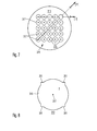
- a long axis of the elliptical shapes may be radially oriented with respect to a center of the aperture pattern, or the long axis may be oriented under an angle to the radial direction. If the long axis is oriented under an angle with respect to the radial direction, such angle may increase with increasing distance from the center of the aperture pattern.
- a diameter of the apertures formed in the multi-aperture plate changes with an increasing distance from a center of the aperture pattern.
- the change of diameters may be such that the diameter of the apertures increases or decreases with increasing distance from the center of the aperture pattern.
- a particle-optical component comprising a first multi-aperture plate made of an insulating substrate and having a plurality of apertures formed therethrough.
- An interior of the apertures formed in the insulating substrate is covered with a conductive layer.
- An advantage of such conductive layer provided in the interior of the apertures is a contribution of the layers to screening stray electric fields originating from adjacent or more distant apertures.
- a conductivity of the layer may be designed such that a sufficient screening will be achieved.
- Such means for removing intermediate beamlets passing through the field correcting apertures may include beam stops arranged at suitable positions across the bundle of desired charged-particle beamlets. Such stop may be advantageously formed by a further multi-aperture plate having formed therein plural apertures which allow the desired beamlets to pass therethrough and having no apertures formed therein at positions corresponding to beam paths of the intermediate beamlets.
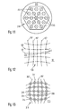
- the shape features of the given beam-manipulating aperture will have a fourfold symmetry about a center of the given aperture for compensating for a non-rotational symmetric field configuration in a volume upstream or downstream of the given beam-manipulating aperture.
- Such non-rotational symmetric field configuration is caused by the symmetry of the beam-manipulating apertures located about the given aperture.
- the beamlets which the particle-optical arrangement is intended to provide do not pass through the field correcting apertures. This does not exclude, however, that intermediate beamlets passing through the field correcting apertures are intercepted by some other means downstream of the field correcting aperture or within the field correcting aperture as described above.
- the apertures in the multi-aperture plate are provided for manipulating charged-particle beamlets passing therethrough.
- a manipulating effect of the apertures is, amongst others, determined by an electric field generated by the multi-aperture plate upstream and/or downstream thereof.
- the single-aperture plate is provided upstream and downstream, respectively, to the multi-aperture plate for shaping the electrical field to a desired shape such that the manipulating effect of the apertures is varied across the aperture pattern according to a desired dependency.
- a second single-aperture plate arranged in-between the multi-aperture plate and the first single-aperture plate.
- a third voltage supply is provided for supplying a predetermined third voltage to the second single-aperture plate.
- the third voltage may be chosen such that it is substantially equal to or lower than the average of the first voltages, or the third voltage may be chosen such that it is in-between the second voltage and the average of the first voltages.
- a first focusing lens is arranged in a beam path of the beam of charged particles in-between the charged-particle source and the multi-aperture plate.
- the first focusing lens has an effect of reducing a divergence of the beam of charged particles generated by the source for illuminating the plurality of apertures formed in the multi-aperture plate with charged particles.
- the charged-particle beam downstream of the first focusing lens may be either a divergent beam or a parallel beam. However, a divergence or parallelity of the beam should correspond to a desired divergence or parallelity to a high accuracy.
- lens errors such as an opening error or a chromatic error, contribute to a deviation from the desired divergence or parallelity.
- a kinetic energy of the electrons impinging on or traversing the multi-aperture plate may be higher than 5 keV, higher than 10 keV, higher than 20 keV or even higher than 30 keV.
- a convergent illumination of the multi-aperture plate is advantageous. Applications for such convergent illuminations may be, in particular, in the field of electron lithography.
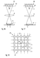
- a distance between adjacent centers of the apertures formed in the multi-aperture plate is a limited distance which may not be further reduced. If such multi-aperture plate is illuminated with a parallel beam, also a distance of adjacent foci of the beamlets downstream of the multi-aperture plate will correspond to the distance between adjacent apertures in the multi-aperture plate.
- the arrangement has a low number of only three necessary magnetic field regions but may be still designed such that, for a given kinetic energy of the primary electrons and a given kinetic energy of the secondary electrons the arrangement provides electron-optical properties which are in first order stigmatic and/or in first order distortion free.
- the magnet arrangement comprises a fourth magnetic field region in the secondary electron beam path downstream of the third magnetic field region, wherein a magnetic field strength in the third magnetic field region is adjustable relative to a magnetic field strength in the first magnetic field region.
- the field strength in the fourth magnetic field region may be adjusted in dependence of the voltage supplied to the pair of electrodes. Since a change of the voltage supplied to the pair of electrodes changes the kinetic energy of the secondary electrons entering the magnet arrangement, the deflection angle of the first magnetic field region for the secondary electron beam path will also change.
- the possibility to adjust the field strength in the third and fourth magnetic field regions provides the possibility to compensate for such changes on the secondary electron beam path caused by changes of the voltage supply to the pair of electrodes.
- the fourth magnetic field region may provide a function of a compensating deflector.
- an intermediate image of the object plane is formed by the secondary electrons in a region comprising the first, third, fourth and fifth magnetic field regions.
- the array 103 of primary electron beam spots 5 is a substantially regular rectangular array with a substantially constant pitch P 1 in a range of 1 ⁇ m to 10 ⁇ m. It is, however, also possible that the array 103 is a distorted regular array or an irregular array or an array of some other symmetry, such as a hexagonal array.
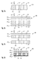
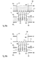
- Figure 2 shows cross sections of some of a plurality of possible embodiments of multi-aperture arrangement 305.
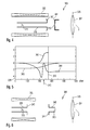
- Figure 5 shows some physical properties of the arrangement 300 of Figure 4 plotted along the z-axis in arbitrary units.
- a curve 342 indicates the decelerating electrical field generated between electrodes 340, 341.
- the voltage supply 361 comprises a constant current source 363 and a plurality of resistors R 1 , R 2 , R 3 ... and a fixed voltage point 364 such that voltages U 0 , U 1 , U 2 differ from each other.
- Constant current I and resistors R 1 , R 2 , ... are chosen such that a focal length of the lens function provided by the respective apertures 315 increases with increasing distance from a center 358 of aperture pattern 319.
- separate voltage sources may be provided for supplying voltages U 0 , U 1 , U 2 , ... to the plate portions 362 1 , 362 2 , ...
- a voltage supply (not shown in Figure 20 ) is provided to supply a voltage of 30 kV in the illustrated example or some other suitable voltage to single-aperture plate 367 1 , a voltage of 9 kV in the illustrated example or some other suitable voltage to multi-aperture plate 313, a voltage of 9 kV to single-aperture plate 367 2 and a voltage of 30 kV to single-aperture plate 367 3 .
- Field lines of electrical field E 1 generated by plates 313 and 367 1 upstream of multi-aperture plate 313 are indicated in Figure 20a as well as field lines of electrical field E 2 generated by plates 313, 367 2 , 367 3 downstream of multi-aperture plate 313.
- the multi-aperture plate 313 is at a lower potential (9 kV) as compared to the outer single-aperture plates 367 1 , 367 3 , respectively (30 kV). This results in a focusing effect of the apertures 315 such that real foci 323 are generated downstream of the multi-aperture plate 313.
- Field portion 403 extends over a length L 1
- drift region extends over a length L 2
- second field portion 407 extends over a length L 3 and a distance between a lower edge of second field portion 407 and object plane 101 is L 4 in the present example.
- L 1 is about 75 mm
- L 2 is about 90 mm
- L 3 is about 60 mm
- L 4 is about 80 mm.
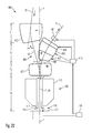
- the absolute values of the field strength in field portions 403 and 407 are about equal, and length L 1 and L 3 of field portions 403 and 407 are chosen such that a spatial dispersion induced by the deflection by the angle a to the left and the subsequent deflection by the angle ⁇ to the right is substantially zero. Further, the field portions 403 and 407 and the drift region 405 are chosen such that the deflections induced by the beam splitter/combiner arrangement 400 on the primary electron beam path 13 are in first order substantially stigmatic and in first order substantially distortion free.
- the pattern 327 of the foci 323 generated by multi-aperture arrangement 305 may be imaged onto the object plane 101 with a high quality. This imaging quality is maintained substantially independent of the landing energy of the primary electrons onto the object 7.
- the secondary electron beam path 11 comprising the plurality of secondary electron beamlets 9 is separated from the primary electron beam path 13 by field region 407 which deflects the secondary electron beam path 11 by an angle ⁇ to the right.
- Deflection angle ⁇ for the secondary electron beam path 11 provided by field region 407 will change, accordingly.
- the secondary electron beam path passes a drift region 409 which is substantially free of magnetic fields before entering a further magnetic field region 411 providing a homogeneous magnetic field deflecting the secondary electron beam path 11 further to the right.
- a field strength of field region 411 may be adjusted by a controller 413.
- the secondary electron beam path 11 immediately enters a further field region 415 providing a homogeneous magnetic field, a field strength of which may be also adjusted by controller 413.
- the changes in the magnetic field strengths of field regions 411, 415 caused by controller 413 result in changes of a quadrupole effect which these electron optical elements 411, 415 have on the secondary electrons.
- a further magnetic field region 419 is provided immediately downstream of field region 415.
- a homogeneous magnetic field is provided, a field strength of which is controlled by controller 413.
- a quadrupole lens 421 is provided downstream of magnetic field region 419 which is controlled by controller 413 to compensate in cooperation with magnetic field region 419 the remaining quadrupole effect induced by field portions 411, 415 when compensating the beam path for different landing energies of the primary electrons.
- a beam deflecting magnetic field region providing a substantial angle of deflection will be a field region providing a deflection angle higher than 5° or higher than 10°.
- the writing beamlets are generated in the beamlet generating arrangement 300 similar to the generation of primary electron beamlets as illustrated with respect to the electron microscopy system above:
- An electron source arrangement 301 generates a diverging electron beam 309 which is collimated by a collimating lens 303 to form a beam 311 for illuminating a multi-aperture arrangement 305. Downstream of the multi-aperture arrangement 305 an array of foci 323 of the writing electron beamlets is formed.
- a beam blanking arrangement 340 for switching the plurality of writing beams selectively on and off.
- the beam blanking arrangement 340 comprises a further multi-aperture plate (not shown in Figure 23 ) arranged such that a respective focus 323 is formed in each aperture thereof.
- Each aperture provides the function of a beam deflector which may be formed by two electrodes on opposite sides of the aperture.
- the electrodes are supplied by voltages controlled by a computer. When no voltage is applied to the electrodes of the aperture, the beamlet passing therethrough will pass along a straight line, i.e. the beamlet will not be deflected.
- a suitable voltage is supplied to the electrodes an electrical field will be generated within the aperture to deflect the respective beamlet by a suitable angle.
- subsequent beam deflectors 451, 452 Downstream of the beam blanking unit there are provided subsequent beam deflectors 451, 452 for displacing the writing beamlets by a distance d with respect to their beam path before traversing the beam deflectors 451, 452.
Landscapes
- Chemical & Material Sciences (AREA)
- Analytical Chemistry (AREA)
- Engineering & Computer Science (AREA)
- Nanotechnology (AREA)
- Physics & Mathematics (AREA)
- Crystallography & Structural Chemistry (AREA)
- Manufacturing & Machinery (AREA)
- General Physics & Mathematics (AREA)
- Condensed Matter Physics & Semiconductors (AREA)
- Mathematical Physics (AREA)
- Theoretical Computer Science (AREA)
- Electron Beam Exposure (AREA)
- Testing Or Measuring Of Semiconductors Or The Like (AREA)
- Analysing Materials By The Use Of Radiation (AREA)
- Exposure And Positioning Against Photoresist Photosensitive Materials (AREA)
Applications Claiming Priority (3)
| Application Number | Priority Date | Filing Date | Title |
|---|---|---|---|
| US50025603P | 2003-09-05 | 2003-09-05 | |
| EP04783363A EP1668662B1 (de) | 2003-09-05 | 2004-09-07 | Optische partikelsysteme und anordnungen und optische partikelkomponenten für solche systeme und anordnungen |
| PCT/US2004/029079 WO2005024881A2 (en) | 2003-09-05 | 2004-09-07 | Particle-optical systems, components and arrangements |
Related Parent Applications (2)
| Application Number | Title | Priority Date | Filing Date |
|---|---|---|---|
| EP04783363A Division EP1668662B1 (de) | 2003-09-05 | 2004-09-07 | Optische partikelsysteme und anordnungen und optische partikelkomponenten für solche systeme und anordnungen |
| EP04783363.7 Division | 2004-09-07 |
Publications (3)
| Publication Number | Publication Date |
|---|---|
| EP2575143A1 true EP2575143A1 (de) | 2013-04-03 |
| EP2575143B1 EP2575143B1 (de) | 2017-11-08 |
| EP2575143B8 EP2575143B8 (de) | 2019-05-22 |
Family
ID=34272938
Family Applications (10)
| Application Number | Title | Priority Date | Filing Date |
|---|---|---|---|
| EP12190690.3A Expired - Lifetime EP2575144B1 (de) | 2003-09-05 | 2004-09-07 | Optische partikelsysteme und anordnungen und optische partikelkomponenten für solche systeme und anordnungen |
| EP12190689.5A Expired - Lifetime EP2575143B8 (de) | 2003-09-05 | 2004-09-07 | Optische Partikelsysteme und Anordnungen und optische Partikelkomponenten für solche Systeme und Anordnungen |
| EP12190692.9A Expired - Lifetime EP2579269B8 (de) | 2003-09-05 | 2004-09-07 | Optische Partikelsysteme und Anordnungen und optische Partikelkomponenten für solche Systeme und Anordnungen |
| EP12190693.7A Expired - Lifetime EP2579270B8 (de) | 2003-09-05 | 2004-09-07 | Optische Partikelsysteme und Anordnungen und optische Partikelkomponenten für solche Systeme und Anordnungen |
| EP12190691.1A Withdrawn EP2579268A1 (de) | 2003-09-05 | 2004-09-07 | Optische Partikelsysteme und Anordnungen und optische Partikelkomponenten für solche Systeme und Anordnungen |
| EP12190694.5A Expired - Lifetime EP2579271B8 (de) | 2003-09-05 | 2004-09-07 | Optische Partikelsysteme und Anordnungen und optische Partikelkomponenten für solche Systeme und Anordnungen |
| EP12190695.2A Withdrawn EP2579272A1 (de) | 2003-09-05 | 2004-09-07 | Optische Partikelsysteme und Anordnungen und optische Partikelkomponenten für solche Systeme und Anordnungen |
| EP12190697.8A Withdrawn EP2579274A1 (de) | 2003-09-05 | 2004-09-07 | Optische Partikelsysteme und Anordnungen und optische Partikelkomponenten für solche Systeme und Anordnungen |
| EP04783363A Expired - Lifetime EP1668662B1 (de) | 2003-09-05 | 2004-09-07 | Optische partikelsysteme und anordnungen und optische partikelkomponenten für solche systeme und anordnungen |
| EP12190696.0A Expired - Lifetime EP2579273B8 (de) | 2003-09-05 | 2004-09-07 | Optische Partikelsysteme und Anordnungen und optische Partikelkomponenten für solche Systeme und Anordnungen |
Family Applications Before (1)
| Application Number | Title | Priority Date | Filing Date |
|---|---|---|---|
| EP12190690.3A Expired - Lifetime EP2575144B1 (de) | 2003-09-05 | 2004-09-07 | Optische partikelsysteme und anordnungen und optische partikelkomponenten für solche systeme und anordnungen |
Family Applications After (8)
| Application Number | Title | Priority Date | Filing Date |
|---|---|---|---|
| EP12190692.9A Expired - Lifetime EP2579269B8 (de) | 2003-09-05 | 2004-09-07 | Optische Partikelsysteme und Anordnungen und optische Partikelkomponenten für solche Systeme und Anordnungen |
| EP12190693.7A Expired - Lifetime EP2579270B8 (de) | 2003-09-05 | 2004-09-07 | Optische Partikelsysteme und Anordnungen und optische Partikelkomponenten für solche Systeme und Anordnungen |
| EP12190691.1A Withdrawn EP2579268A1 (de) | 2003-09-05 | 2004-09-07 | Optische Partikelsysteme und Anordnungen und optische Partikelkomponenten für solche Systeme und Anordnungen |
| EP12190694.5A Expired - Lifetime EP2579271B8 (de) | 2003-09-05 | 2004-09-07 | Optische Partikelsysteme und Anordnungen und optische Partikelkomponenten für solche Systeme und Anordnungen |
| EP12190695.2A Withdrawn EP2579272A1 (de) | 2003-09-05 | 2004-09-07 | Optische Partikelsysteme und Anordnungen und optische Partikelkomponenten für solche Systeme und Anordnungen |
| EP12190697.8A Withdrawn EP2579274A1 (de) | 2003-09-05 | 2004-09-07 | Optische Partikelsysteme und Anordnungen und optische Partikelkomponenten für solche Systeme und Anordnungen |
| EP04783363A Expired - Lifetime EP1668662B1 (de) | 2003-09-05 | 2004-09-07 | Optische partikelsysteme und anordnungen und optische partikelkomponenten für solche systeme und anordnungen |
| EP12190696.0A Expired - Lifetime EP2579273B8 (de) | 2003-09-05 | 2004-09-07 | Optische Partikelsysteme und Anordnungen und optische Partikelkomponenten für solche Systeme und Anordnungen |
Country Status (6)
| Country | Link |
|---|---|
| US (7) | US7244949B2 (de) |
| EP (10) | EP2575144B1 (de) |
| JP (6) | JP4794444B2 (de) |
| KR (1) | KR101051370B1 (de) |
| CN (3) | CN101103417B (de) |
| WO (1) | WO2005024881A2 (de) |
Cited By (7)
| Publication number | Priority date | Publication date | Assignee | Title |
|---|---|---|---|---|
| EP3869533A1 (de) | 2020-02-21 | 2021-08-25 | ASML Netherlands B.V. | Inspektionswerkzeug mit geladenen teilchen, inspektionsverfahren |
| EP3869536A1 (de) | 2020-02-21 | 2021-08-25 | ASML Netherlands B.V. | Inspektionsvorrichtung |
| WO2021165135A1 (en) | 2020-02-21 | 2021-08-26 | Asml Netherlands B.V. | Inspection apparatus |
| EP3893263A1 (de) | 2020-04-06 | 2021-10-13 | ASML Netherlands B.V. | Blendenanordnung, strahlmanipulatoreinheit, verfahren zum manipulieren geladener teilchenstrahlen und geladene teilchenprojektionsvorrichtung |
| EP3937205A1 (de) | 2020-07-06 | 2022-01-12 | ASML Netherlands B.V. | Ladungsteilchenmehrstrahlsäule, ladungsteilchenmehrstrahlsäulenanordnung, inspektionsverfahren |
| EP4102535A1 (de) | 2021-06-08 | 2022-12-14 | ASML Netherlands B.V. | Ladungsteilchenvorrichtung und -verfahren |
| WO2022258271A1 (en) | 2021-06-08 | 2022-12-15 | Asml Netherlands B.V. | Charged particle apparatus and method |
Families Citing this family (235)
| Publication number | Priority date | Publication date | Assignee | Title |
|---|---|---|---|---|
| EP2575144B1 (de) | 2003-09-05 | 2017-07-12 | Carl Zeiss Microscopy GmbH | Optische partikelsysteme und anordnungen und optische partikelkomponenten für solche systeme und anordnungen |
| EP1619495A1 (de) * | 2004-07-23 | 2006-01-25 | Nederlandse Organisatie voor toegepast-natuurwetenschappelijk Onderzoek TNO | Verfahren und Vorrichtung zur Kontrolle einer Probenoberfläche und Verwendung von fluoreszierenden Materialien |
| GB0425290D0 (en) * | 2004-11-17 | 2004-12-15 | Eastham Derek A | Focussing masks |
| US7468507B2 (en) | 2005-01-26 | 2008-12-23 | Applied Materials, Israel, Ltd. | Optical spot grid array scanning system |
| US7468506B2 (en) | 2005-01-26 | 2008-12-23 | Applied Materials, Israel, Ltd. | Spot grid array scanning system |
| EP1851784B8 (de) | 2005-02-11 | 2016-10-19 | IMS Nanofabrication AG | Vorrichtung zur belichtung mit geladenen teilchen mit elektrostatischer zonenplatte |
| JP2007019192A (ja) * | 2005-07-06 | 2007-01-25 | Canon Inc | 荷電ビームレンズ、及び荷電ビーム露光装置 |
| EP1753010B1 (de) | 2005-08-09 | 2012-12-05 | Carl Zeiss SMS GmbH | Teilchenoptisches System |
| JP5222142B2 (ja) * | 2005-09-06 | 2013-06-26 | カール・ツァイス・エスエムティー・ゲーエムベーハー | 粒子光学部品 |
| JP5159035B2 (ja) * | 2005-10-28 | 2013-03-06 | キヤノン株式会社 | レンズアレイ及び該レンズアレイを含む荷電粒子線露光装置 |
| KR101589306B1 (ko) | 2005-11-28 | 2016-01-27 | 칼 짜이스 에스엠테 게엠베하 | 입자 광학 구성요소 |
| TWI432908B (zh) * | 2006-03-10 | 2014-04-01 | 瑪波微影Ip公司 | 微影系統及投射方法 |
| CN101443877A (zh) * | 2006-03-27 | 2009-05-27 | 多束系统公司 | 用于生成高电流密度构图带电粒子束的光学器件 |
| JP2007287365A (ja) * | 2006-04-13 | 2007-11-01 | Jeol Ltd | 多極子レンズ及び多極子レンズの製造方法 |
| JP4878501B2 (ja) * | 2006-05-25 | 2012-02-15 | 株式会社日立ハイテクノロジーズ | 荷電粒子線応用装置 |
| EP2044610B1 (de) | 2006-07-20 | 2012-11-28 | SPP Process Technology Systems UK Limited | Plasmaquellen |
| CN101490792B (zh) * | 2006-07-20 | 2012-02-01 | 阿维扎技术有限公司 | 离子沉积设备 |
| US8354652B2 (en) | 2006-07-20 | 2013-01-15 | Aviza Technology Limited | Ion source including separate support systems for accelerator grids |
| EP2050118A1 (de) * | 2006-07-25 | 2009-04-22 | Mapper Lithography IP B.V. | Optisches system mit mehreren strahlengeladenen teilchen |
| US8134135B2 (en) | 2006-07-25 | 2012-03-13 | Mapper Lithography Ip B.V. | Multiple beam charged particle optical system |
| JP2008066359A (ja) * | 2006-09-05 | 2008-03-21 | Canon Inc | 荷電ビームレンズアレイ、露光装置及びデバイス製造方法 |
| US7763851B2 (en) * | 2006-12-22 | 2010-07-27 | Ims Nanofabrication Ag | Particle-beam apparatus with improved wien-type filter |
| JP5227512B2 (ja) * | 2006-12-27 | 2013-07-03 | 株式会社日立ハイテクノロジーズ | 電子線応用装置 |
| US8421305B2 (en) * | 2007-04-17 | 2013-04-16 | The University Of Utah Research Foundation | MEMS devices and systems actuated by an energy field |
| EP2019415B1 (de) * | 2007-07-24 | 2016-05-11 | IMS Nanofabrication AG | Mehrfachstrahlquelle |
| US8642959B2 (en) * | 2007-10-29 | 2014-02-04 | Micron Technology, Inc. | Method and system of performing three-dimensional imaging using an electron microscope |
| NL2003304C2 (en) * | 2008-08-07 | 2010-09-14 | Ims Nanofabrication Ag | Compensation of dose inhomogeneity and image distortion. |
| KR100946270B1 (ko) * | 2008-08-12 | 2010-03-09 | 주식회사 메가젠임플란트 | 연조직 절단 치과용 공구 |
| JP5484808B2 (ja) * | 2008-09-19 | 2014-05-07 | 株式会社ニューフレアテクノロジー | 描画装置及び描画方法 |
| EP2406810B1 (de) * | 2008-10-01 | 2014-09-17 | Mapper Lithography IP B.V. | Elektrostatische linsenstruktur |
| GB0912332D0 (en) * | 2009-07-16 | 2009-08-26 | Vg Systems Ltd | Magnetic lens,method for focussing charged particles and charged particle energy analyser |
| US8546767B2 (en) * | 2010-02-22 | 2013-10-01 | Ims Nanofabrication Ag | Pattern definition device with multiple multibeam array |
| EP2556527B1 (de) | 2010-04-09 | 2017-03-22 | Carl Zeiss Microscopy GmbH | System zur erkennung von geladenen partikeln und inspektionssystem mit mehreren teilstrahlen |
| WO2011148486A1 (ja) * | 2010-05-27 | 2011-12-01 | 三菱電機株式会社 | 粒子線照射システムおよび粒子線照射システムの制御方法 |
| DE102010026169B4 (de) * | 2010-07-06 | 2014-09-04 | Carl Zeiss Microscopy Gmbh | Partikelstrahlsystem |
| WO2012025546A1 (en) * | 2010-08-26 | 2012-03-01 | Tetra Laval Holdings & Finance S.A. | Control grid design for an electron beam generating device |
| WO2012041464A1 (en) | 2010-09-28 | 2012-04-05 | Applied Materials Israel Ltd. | Particle-optical systems and arrangements and particle-optical components for such systems and arrangements |
| EP2625306B1 (de) * | 2010-10-05 | 2020-09-30 | Veeco Instruments Inc. | Gitter mit beamlet-lenkung |
| US8294095B2 (en) | 2010-12-14 | 2012-10-23 | Hermes Microvision, Inc. | Apparatus of plural charged particle beams with multi-axis magnetic lens |
| US9530613B2 (en) * | 2011-02-18 | 2016-12-27 | Applied Materials Israel, Ltd. | Focusing a charged particle system |
| NL2007604C2 (en) * | 2011-10-14 | 2013-05-01 | Mapper Lithography Ip Bv | Charged particle system comprising a manipulator device for manipulation of one or more charged particle beams. |
| US9702983B2 (en) | 2011-05-03 | 2017-07-11 | Applied Materials Israel, Ltd. | Multi-spot collection optics |
| JP2012238770A (ja) * | 2011-05-12 | 2012-12-06 | Canon Inc | 静電レンズアレイ、描画装置、及びデバイスの製造方法 |
| US8933425B1 (en) * | 2011-11-02 | 2015-01-13 | Kla-Tencor Corporation | Apparatus and methods for aberration correction in electron beam based system |
| JP5886663B2 (ja) * | 2012-03-21 | 2016-03-16 | 株式会社日立ハイテクノロジーズ | 電子線応用装置およびレンズアレイ |
| RU2606234C2 (ru) | 2012-05-31 | 2017-01-10 | Сименс Акциенгезелльшафт | Отклоняющая пластина и отклоняющее устройство для отклонения заряженных частиц |
| NL2009053C2 (en) | 2012-06-22 | 2013-12-24 | Univ Delft Tech | Apparatus and method for inspecting a surface of a sample. |
| US10413755B1 (en) | 2012-08-01 | 2019-09-17 | Velayudhan Sahadevan | Device and methods for adaptive resistance inhibiting proton and carbon ion microbeams and nanobeams radiosurgery |
| US9001308B2 (en) * | 2013-02-01 | 2015-04-07 | Taiwan Semiconductor Manufacturing Company, Ltd. | Pattern generator for a lithography system |
| JP6208451B2 (ja) * | 2013-03-29 | 2017-10-04 | 国立大学法人東北大学 | 回路基板、電子ビーム発生装置、電子ビーム照射装置、電子ビーム露光装置、および製造方法 |
| WO2014156171A1 (ja) * | 2013-03-29 | 2014-10-02 | 国立大学法人東北大学 | 複数の電子ビームを制御する際に確実に動作する回路基板 |
| JP2014197652A (ja) * | 2013-03-29 | 2014-10-16 | 国立大学法人東北大学 | 回路基板、電子ビーム発生装置、電子ビーム照射装置、電子ビーム露光装置、および製造方法 |
| DE102013006535B4 (de) * | 2013-04-15 | 2025-11-06 | Carl Zeiss Microscopy Gmbh | Raster-Partikelstrahlmikroskop mit energiefilterndem Detektorsystem |
| CN104345331B (zh) * | 2013-07-24 | 2017-04-19 | 中国科学院上海微系统与信息技术研究所 | 图像型电子自旋分析器 |
| DE102013014976A1 (de) | 2013-09-09 | 2015-03-12 | Carl Zeiss Microscopy Gmbh | Teilchenoptisches System |
| DE102013016113B4 (de) | 2013-09-26 | 2018-11-29 | Carl Zeiss Microscopy Gmbh | Verfahren zum Detektieren von Elektronen, Elektronendetektor und Inspektionssystem |
| US9263233B2 (en) | 2013-09-29 | 2016-02-16 | Carl Zeiss Microscopy Gmbh | Charged particle multi-beam inspection system and method of operating the same |
| EP3454357B1 (de) | 2013-09-30 | 2020-08-12 | Carl Zeiss Microscopy GmbH | Geladenes teilchenstrahlsystem und verfahren zum betrieb davon |
| DE102014008105B4 (de) | 2014-05-30 | 2021-11-11 | Carl Zeiss Multisem Gmbh | Mehrstrahl-Teilchenmikroskop |
| DE102014008083B9 (de) | 2014-05-30 | 2018-03-22 | Carl Zeiss Microscopy Gmbh | Teilchenstrahlsystem |
| DE102014008383B9 (de) | 2014-06-06 | 2018-03-22 | Carl Zeiss Microscopy Gmbh | Teilchenstrahlsystem und Verfahren zum Betreiben einer Teilchenoptik |
| NL2013411B1 (en) * | 2014-09-04 | 2016-09-27 | Univ Delft Tech | Multi electron beam inspection apparatus. |
| DE102015202172B4 (de) | 2015-02-06 | 2017-01-19 | Carl Zeiss Microscopy Gmbh | Teilchenstrahlsystem und Verfahren zur teilchenoptischen Untersuchung eines Objekts |
| US9691588B2 (en) | 2015-03-10 | 2017-06-27 | Hermes Microvision, Inc. | Apparatus of plural charged-particle beams |
| US10236156B2 (en) | 2015-03-25 | 2019-03-19 | Hermes Microvision Inc. | Apparatus of plural charged-particle beams |
| US9607805B2 (en) | 2015-05-12 | 2017-03-28 | Hermes Microvision Inc. | Apparatus of plural charged-particle beams |
| KR102441581B1 (ko) | 2015-06-03 | 2022-09-07 | 삼성전자주식회사 | 표면 검사 방법 및 이를 이용한 포토 마스크의 검사 방법 |
| US9922799B2 (en) | 2015-07-21 | 2018-03-20 | Hermes Microvision, Inc. | Apparatus of plural charged-particle beams |
| IL294759B2 (en) | 2015-07-22 | 2024-09-01 | Asml Netherlands Bv | Device for multiple charged particle beams |
| US10192716B2 (en) * | 2015-09-21 | 2019-01-29 | Kla-Tencor Corporation | Multi-beam dark field imaging |
| US10460905B2 (en) | 2015-09-23 | 2019-10-29 | Kla-Tencor Corporation | Backscattered electrons (BSE) imaging using multi-beam tools |
| JP6132448B2 (ja) * | 2015-11-26 | 2017-05-24 | 京楽産業.株式会社 | 遊技機 |
| JP6641011B2 (ja) | 2015-11-30 | 2020-02-05 | エーエスエムエル ネザーランズ ビー.ブイ. | 複数の荷電粒子ビームの装置 |
| JP2017134927A (ja) * | 2016-01-26 | 2017-08-03 | 株式会社荏原製作所 | 検査装置 |
| KR102480232B1 (ko) * | 2016-01-27 | 2022-12-22 | 에이에스엠엘 네델란즈 비.브이. | 복수의 하전 입자 빔들의 장치 |
| US11302511B2 (en) * | 2016-02-04 | 2022-04-12 | Kla Corporation | Field curvature correction for multi-beam inspection systems |
| US10395883B2 (en) * | 2016-03-31 | 2019-08-27 | Intel Corporation | Aperture size modulation to enhance ebeam patterning resolution |
| JP6550478B2 (ja) * | 2016-04-13 | 2019-07-24 | エーエスエムエル ネザーランズ ビー.ブイ. | マルチビーム装置、荷電粒子ビーム装置、ソース変換ユニット、ソース変換ユニットを構成する方法、仮想的マルチソースアレイを形成するための方法 |
| US10418324B2 (en) | 2016-10-27 | 2019-09-17 | Asml Netherlands B.V. | Fabricating unique chips using a charged particle multi-beamlet lithography system |
| DE102016120902B4 (de) | 2016-11-02 | 2018-08-23 | Carl Zeiss Microscopy Gmbh | Vielstrahl-Teilchenmikroskop |
| US10453645B2 (en) * | 2016-12-01 | 2019-10-22 | Applied Materials Israel Ltd. | Method for inspecting a specimen and charged particle multi-beam device |
| US9922796B1 (en) * | 2016-12-01 | 2018-03-20 | Applied Materials Israel Ltd. | Method for inspecting a specimen and charged particle multi-beam device |
| CN110268330B (zh) * | 2016-12-23 | 2022-01-28 | Asml荷兰有限公司 | 一种使用无掩模光刻曝光系统制造电子器件的方法和系统 |
| US10840056B2 (en) * | 2017-02-03 | 2020-11-17 | Kla Corporation | Multi-column scanning electron microscopy system |
| US10347460B2 (en) | 2017-03-01 | 2019-07-09 | Dongfang Jingyuan Electron Limited | Patterned substrate imaging using multiple electron beams |
| JP7108618B2 (ja) | 2017-03-20 | 2022-07-28 | カール ツァイス マルチセム ゲーエムベーハー | 荷電粒子ビームシステムおよび方法 |
| US10923315B2 (en) | 2017-03-24 | 2021-02-16 | Hitachi High-Tech Corporation | Charged particle beam apparatus, and method of adjusting charged particle beam apparatus |
| JP6959989B2 (ja) | 2017-04-28 | 2021-11-05 | エーエスエムエル ネザーランズ ビー.ブイ. | 荷電粒子の複数のビームを使用した装置 |
| EP3630391A1 (de) | 2017-05-22 | 2020-04-08 | Howmedica Osteonics Corp. | Vorrichtung zur in-situ-herstellungsprozessüberwachung und rückkopplungssteuerung eines generativen fertigungsprozesses mit elektronenstrahl |
| KR20240042162A (ko) | 2017-07-28 | 2024-04-01 | 에이에스엠엘 네델란즈 비.브이. | 단일-빔 또는 멀티-빔 장치에서의 빔 분리기의 분산을 보상하기 위한 시스템들 및 방법들 |
| JP6819509B2 (ja) * | 2017-08-10 | 2021-01-27 | 株式会社ニューフレアテクノロジー | マルチ荷電粒子ビーム描画装置 |
| US20190066972A1 (en) * | 2017-08-29 | 2019-02-28 | ICT Integrated Circuit Testing Gesellschaft für Halbleiterprüftechnik mbH | Charged particle beam device, aperture arrangement for a charged particle beam device, and method for operating a charged particle beam device |
| WO2019048293A1 (en) | 2017-09-07 | 2019-03-14 | Asml Netherlands B.V. | METHODS OF INSPECTING SAMPLES WITH MULTIPLE BEAMS OF CHARGED PARTICLES |
| KR102650064B1 (ko) * | 2017-09-29 | 2024-03-22 | 에이에스엠엘 네델란즈 비.브이. | 다중 하전 입자 빔으로 샘플을 검사하는 방법 |
| US11164719B2 (en) | 2017-09-29 | 2021-11-02 | Asml Netherlands B.V. | Image contrast enhancement in sample inspection |
| WO2019063559A1 (en) | 2017-09-29 | 2019-04-04 | Asml Netherlands B.V. | DYNAMIC DETERMINATION OF A CHARGED PARTICLE BEAM INSPECTION SAMPLE INSPECTION RECIPE |
| US20190104606A1 (en) * | 2017-10-02 | 2019-04-04 | Rayton Solar Inc. | Systems and processes for producing relatively uniform transverse irradiation fields of charged-particle beams |
| CN111107937B (zh) * | 2017-10-18 | 2022-08-02 | 核酸有限公司 | 包括具有薄膜晶体管和电容感测的双基底的数字微流体设备 |
| KR102444288B1 (ko) | 2017-11-08 | 2022-09-16 | 삼성전자주식회사 | 메타 렌즈를 포함하는 프로젝터 |
| US11373321B2 (en) | 2017-11-08 | 2022-06-28 | Samsung Electronics Co., Ltd. | Projector including meta-lens |
| JP6966319B2 (ja) * | 2017-12-22 | 2021-11-17 | 株式会社ニューフレアテクノロジー | マルチビーム画像取得装置及びマルチビーム画像取得方法 |
| DE102018202428B3 (de) | 2018-02-16 | 2019-05-09 | Carl Zeiss Microscopy Gmbh | Vielstrahl-Teilchenmikroskop |
| DE102018202421B3 (de) | 2018-02-16 | 2019-07-11 | Carl Zeiss Microscopy Gmbh | Vielstrahl-Teilchenstrahlsystem |
| US10504683B2 (en) * | 2018-02-22 | 2019-12-10 | ICT Integrated Circuit Testing Gesellschaft für Halbleiterprüftechnik mbH | Device and method for forming a plurality of charged particle beamlets |
| CN112055886A (zh) | 2018-02-27 | 2020-12-08 | 卡尔蔡司MultiSEM有限责任公司 | 带电粒子多束系统及方法 |
| WO2019186937A1 (ja) * | 2018-03-29 | 2019-10-03 | 株式会社日立ハイテクノロジーズ | 荷電粒子線装置 |
| IL277822B2 (en) | 2018-05-01 | 2024-08-01 | Asml Netherlands Bv | Multi-beam test rig |
| US10811215B2 (en) | 2018-05-21 | 2020-10-20 | Carl Zeiss Multisem Gmbh | Charged particle beam system |
| EP3576128A1 (de) * | 2018-05-28 | 2019-12-04 | ASML Netherlands B.V. | Elektronenstrahlvorrichtung, prüfwerkzeug und prüfverfahren |
| US11087950B2 (en) * | 2018-05-29 | 2021-08-10 | Kla-Tencor Corporation | Charge control device for a system with multiple electron beams |
| US10770262B1 (en) * | 2018-05-30 | 2020-09-08 | National Technology & Engineering Solutions Of Sandia, Llc | Apparatus, method and system for imaging and utilization of SEM charged particles |
| DE102018115012A1 (de) * | 2018-06-21 | 2019-12-24 | Carl Zeiss Microscopy Gmbh | Teilchenstrahlsystem |
| AU2019206103B2 (en) | 2018-07-19 | 2025-06-26 | Howmedica Osteonics Corp. | System and process for in-process electron beam profile and location analyses |
| EP3834222A1 (de) * | 2018-08-09 | 2021-06-16 | ASML Netherlands B.V. | Vorrichtung für mehrere ladungsteilchenstrahlen |
| EP3624167A1 (de) * | 2018-09-14 | 2020-03-18 | FEI Company | Bildgebungsvorrichtung mit multi-elektronen-strahl mit verbesserter leistung |
| DE102018007455B4 (de) | 2018-09-21 | 2020-07-09 | Carl Zeiss Multisem Gmbh | Verfahren zum Detektorabgleich bei der Abbildung von Objekten mittels eines Mehrstrahl-Teilchenmikroskops, System sowie Computerprogrammprodukt |
| DE102018007652B4 (de) * | 2018-09-27 | 2021-03-25 | Carl Zeiss Multisem Gmbh | Teilchenstrahl-System sowie Verfahren zur Stromregulierung von Einzel-Teilchenstrahlen |
| DE102018124044B3 (de) | 2018-09-28 | 2020-02-06 | Carl Zeiss Microscopy Gmbh | Verfahren zum Betreiben eines Vielstrahl-Teilchenstrahlmikroskops und Vielstrahl-Teilchenstrahlsystem |
| DE102018124219A1 (de) | 2018-10-01 | 2020-04-02 | Carl Zeiss Microscopy Gmbh | Vielstrahl-Teilchenstrahlsystem und Verfahren zum Betreiben eines solchen |
| DE102018124401A1 (de) | 2018-10-02 | 2020-04-02 | Carl Zeiss Smt Gmbh | Verfahren zum Aufnehmen eines Bildes mit einem Teilchenmikroskop |
| US10784070B2 (en) * | 2018-10-19 | 2020-09-22 | ICT Integrated Circuit Testing Gesellschaft für Halbleiterprüftechnik mbH | Charged particle beam device, field curvature corrector, and methods of operating a charged particle beam device |
| US11145485B2 (en) * | 2018-12-26 | 2021-10-12 | Nuflare Technology, Inc. | Multiple electron beams irradiation apparatus |
| DE102018133703B4 (de) | 2018-12-29 | 2020-08-06 | Carl Zeiss Multisem Gmbh | Vorrichtung zur Erzeugung einer Vielzahl von Teilchenstrahlen und Vielstrahl-Teilchenstrahlsysteme |
| TWI743626B (zh) | 2019-01-24 | 2021-10-21 | 德商卡爾蔡司多重掃描電子顯微鏡有限公司 | 包含多束粒子顯微鏡的系統、對3d樣本逐層成像之方法及電腦程式產品 |
| CN111477530B (zh) | 2019-01-24 | 2023-05-05 | 卡尔蔡司MultiSEM有限责任公司 | 利用多束粒子显微镜对3d样本成像的方法 |
| US10741355B1 (en) | 2019-02-04 | 2020-08-11 | Carl Zeiss Multisem Gmbh | Multi-beam charged particle system |
| EP3828914A1 (de) * | 2019-02-27 | 2021-06-02 | FEI Company | Ladungsteilchenstrahlvorrichtung zur inspektion einer probe mit einer vielzahl von ladungsteilchenteilstrahlen |
| JP7175798B2 (ja) * | 2019-03-01 | 2022-11-21 | 株式会社荏原製作所 | 荷電粒子マルチビーム装置 |
| TWI737117B (zh) | 2019-03-05 | 2021-08-21 | 日商紐富來科技股份有限公司 | 多電子束照射裝置 |
| JP7241570B2 (ja) * | 2019-03-06 | 2023-03-17 | 株式会社ニューフレアテクノロジー | マルチ電子ビーム検査装置及びマルチ電子ビーム検査方法 |
| JP7265646B2 (ja) * | 2019-03-27 | 2023-04-26 | エーエスエムエル ネザーランズ ビー.ブイ. | マルチビーム検査装置における二次ビームのアライメントのためのシステム及び方法 |
| CN113795459B (zh) | 2019-04-06 | 2025-04-29 | Asml荷兰有限公司 | 具有内置电压生成器的mems图像形成元件 |
| WO2020239504A1 (en) * | 2019-05-28 | 2020-12-03 | Asml Netherlands B.V. | Multiple charged-particle beam apparatus |
| KR102677409B1 (ko) * | 2019-05-31 | 2024-06-25 | 에이에스엠엘 네델란즈 비.브이. | 다중 하전 입자 빔 장치 및 그 작동 방법 |
| DE102019004124B4 (de) * | 2019-06-13 | 2024-03-21 | Carl Zeiss Multisem Gmbh | Teilchenstrahl-System zur azimutalen Ablenkung von Einzel-Teilchenstrahlen sowie seine Verwendung und Verfahren zur Azimut-Korrektur bei einem Teilchenstrahl-System |
| JP7316106B2 (ja) * | 2019-06-14 | 2023-07-27 | 株式会社ニューフレアテクノロジー | 収差補正器及びマルチ電子ビーム照射装置 |
| JP7234052B2 (ja) | 2019-06-28 | 2023-03-07 | 株式会社ニューフレアテクノロジー | マルチ電子ビーム画像取得装置及びマルチ電子ビーム画像取得方法 |
| DE102019005362A1 (de) | 2019-07-31 | 2021-02-04 | Carl Zeiss Multisem Gmbh | Verfahren zum Betreiben eines Vielzahl-Teilchenstrahlsystems unter Veränderung der numerischen Apertur, zugehöriges Computerprogrammprodukt und Vielzahl-Teilchenstrahlsystem |
| DE102019005364B3 (de) | 2019-07-31 | 2020-10-08 | Carl Zeiss Multisem Gmbh | System-Kombination eines Teilchenstrahlsystem und eines lichtoptischen Systems mit kollinearer Strahlführung sowie Verwendung der System-Kombination |
| JP7008671B2 (ja) * | 2019-09-13 | 2022-01-25 | 日本電子株式会社 | 荷電粒子線装置および分析方法 |
| JP7360871B2 (ja) * | 2019-09-24 | 2023-10-13 | 株式会社日立ハイテクサイエンス | 荷電粒子ビーム照射装置、及び制御方法 |
| WO2021071357A1 (en) * | 2019-10-08 | 2021-04-15 | Technische Universiteit Delft | Device for generating a plurality of charged particle beamlets, and an inspection imaging or processing apparatus and method for using the same. |
| US10923313B1 (en) * | 2019-10-17 | 2021-02-16 | ICT Integrated Circuit Testing Gesellschaft für Halbleiterprüftechnik mbH | Charged particle beam device and method of operating a charged particle beam device |
| NL2024065B1 (en) * | 2019-10-21 | 2021-06-22 | Univ Delft Tech | Multi-beam charged particle source with alignment means |
| DE102019008249B3 (de) | 2019-11-27 | 2020-11-19 | Carl Zeiss Multisem Gmbh | Teilchenstrahl-System mit einer Multistrahl-Ablenkeinrichtung und einem Strahlfänger, Verfahren zum Betreiben des Teilchenstrahl-Systems und zugehöriges Computerprogrammprodukt |
| DE102019218315B3 (de) | 2019-11-27 | 2020-10-01 | Carl Zeiss Microscopy Gmbh | Verfahren zur Spannungskontrastbildgebung mit einem Korpuskularvielstrahlmikroskop, Korpuskularvielstrahlmikroskop für Spannungskontrastbildgebung und Halbleiterstrukturen zur Spannungskontrastbildgebung mit einem Korpuskularvielstrahlmikroskop |
| TWI773030B (zh) * | 2019-12-20 | 2022-08-01 | 荷蘭商Asml荷蘭公司 | 用於多射束檢測系統之多模操作 |
| EP3852127A1 (de) | 2020-01-06 | 2021-07-21 | ASML Netherlands B.V. | Ladungsteilchenbeurteilungswerkzeug, inspektionsverfahren |
| WO2021156198A1 (en) | 2020-02-04 | 2021-08-12 | Carl Zeiss Multisem Gmbh | Multi-beam digital scan and image acquisition |
| EP4734148A2 (de) | 2020-03-12 | 2026-04-29 | Carl Zeiss MultiSEM GmbH | Bestimmte verbesserungen von mehrstrahlerzeugungs- und mehrstrahlablenkeinheiten |
| JP7359050B2 (ja) * | 2020-03-18 | 2023-10-11 | 株式会社ニューフレアテクノロジー | マルチビーム用のブランキング装置及びマルチ荷電粒子ビーム描画装置 |
| DE102020107738B3 (de) | 2020-03-20 | 2021-01-14 | Carl Zeiss Multisem Gmbh | Teilchenstrahl-System mit einer Multipol-Linsen-Sequenz zur unabhängigen Fokussierung einer Vielzahl von Einzel-Teilchenstrahlen, seine Verwendung und zugehöriges Verfahren |
| KR102823383B1 (ko) * | 2020-04-03 | 2025-06-20 | 에이에스엠엘 네델란즈 비.브이. | 하전 입자 빔 검사 시 전하 축적 감소에 기초한 이미지 향상 |
| JP7428578B2 (ja) * | 2020-04-22 | 2024-02-06 | 株式会社ホロン | マルチビーム画像生成装置およびマルチビーム画像生成方法 |
| US12525426B2 (en) | 2020-05-01 | 2026-01-13 | Asml Netherlands B.V. | Enhanced architecture for high-performance detection device |
| CN115917700B (zh) | 2020-05-28 | 2026-04-24 | Asml荷兰有限公司 | 用于高性能检测设备技术领域的增强架构 |
| TWI852275B (zh) | 2020-05-28 | 2024-08-11 | 德商卡爾蔡司多重掃描電子顯微鏡有限公司 | 多重射束帶電粒子顯微鏡或系統與其操作方法 |
| DE102020115183B4 (de) | 2020-06-08 | 2026-01-29 | Carl Zeiss Multisem Gmbh | Teilchenstrahlsystem mit Multiquellensystem sowie Mehrstrahl-Teilchenmikroskop |
| DE102020121132B3 (de) | 2020-08-11 | 2021-09-23 | Carl Zeiss Multisem Gmbh | Verfahren zum Betreiben eines Vielzahl-Teilchenstrahlsystems mit einem Spiegel-Betriebsmodus und zugehöriges Computerprogrammprodukt |
| DE102020123567B4 (de) | 2020-09-09 | 2025-02-13 | Carl Zeiss Multisem Gmbh | Vielzahl-Teilchenstrahl-System mit Kontrast-Korrektur-Linsen-System |
| DE102020125534B3 (de) | 2020-09-30 | 2021-12-02 | Carl Zeiss Multisem Gmbh | Vielzahl-Teilchenstrahlmikroskop und zugehöriges Verfahren mit schnellem Autofokus um einen einstellbaren Arbeitsabstand |
| DE102021105201B4 (de) | 2021-03-04 | 2024-10-02 | Carl Zeiss Multisem Gmbh | Vielzahl-Teilchenstrahlmikroskop und zugehöriges Verfahren mit schnellem Autofokus mit speziellen Ausführungen |
| TW202220012A (zh) | 2020-09-30 | 2022-05-16 | 德商卡爾蔡司多重掃描電子顯微鏡有限公司 | 在可調工作距離附近具快速自動對焦之多重粒子束顯微鏡及相關方法 |
| EP4002421A1 (de) * | 2020-11-12 | 2022-05-25 | ASML Netherlands B.V. | Objektivlinsengruppenanordnung, elektronenoptisches system, elektronenoptisches systemarray, verfahren zur fokussierung |
| IL302654A (en) * | 2020-11-12 | 2023-07-01 | Asml Netherlands Bv | Assembling an objective lens array, electronic-optical system, electronic-optical system array, focusing method |
| IL303983A (en) * | 2020-12-23 | 2023-08-01 | Asml Netherlands Bv | Charged particle optical device |
| DE102021200799B3 (de) | 2021-01-29 | 2022-03-31 | Carl Zeiss Multisem Gmbh | Verfahren mit verbesserter Fokuseinstellung unter Berücksichtigung eines Bildebenenkipps in einem Vielzahl-Teilchenstrahlmikroskop |
| CN116888605B (zh) * | 2021-04-30 | 2025-12-05 | 华为技术有限公司 | 神经网络模型的运算方法、训练方法及装置 |
| WO2022238137A1 (en) * | 2021-05-12 | 2022-11-17 | Asml Netherlands B.V. | Assessment system, method of assessing |
| EP4095881A1 (de) * | 2021-05-25 | 2022-11-30 | ASML Netherlands B.V. | Ladungsteilchenvorrichtung |
| TW202312205A (zh) | 2021-05-27 | 2023-03-16 | 德商卡爾蔡司多重掃描電子顯微鏡有限公司 | 多重射束帶電粒子系統與在多重射束帶電粒子系統中控制工作距離的方法 |
| DE102021205394B4 (de) | 2021-05-27 | 2022-12-08 | Carl Zeiss Multisem Gmbh | Verfahren zum Betrieb eines Vielstrahlmikroskops mit an eine Inspektionsstelle angepassten Einstellungen |
| JP7795055B2 (ja) * | 2021-06-16 | 2026-01-07 | カール ツァイス マルティセム ゲゼルシヤフト ミット ベシュレンクテル ハフツング | 歪み最適化マルチビーム走査システム |
| DE102021116969B3 (de) | 2021-07-01 | 2022-09-22 | Carl Zeiss Multisem Gmbh | Verfahren zur bereichsweisen Probeninspektion mittels eines Vielstrahl-Teilchenmikroskopes, Computerprogrammprodukt und Vielstrahl-Teilchenmikroskop zur Halbleiterprobeninspektion |
| DE102021118561B4 (de) * | 2021-07-19 | 2023-03-30 | Carl Zeiss Multisem Gmbh | Verfahren zum Betreiben eines Vielstrahl-Teilchenmikroskopes mit schneller Strahlstromregelung, Computerprogrammprodukt und Vielstrahl-Teilchenmikroskop |
| DE102021118684B4 (de) | 2021-07-20 | 2024-11-28 | Carl Zeiss Multisem Gmbh | Verfahren zur Analyse von Störeinflüssen bei einem Vielstrahl-Teilchenmikroskop, zugehöriges Computerprogrammprodukt und Vielstrahl-Teilchenmikroskop |
| DE102021119008A1 (de) | 2021-07-30 | 2023-02-02 | Carl Zeiss Multisem Gmbh | Verfahren zur Defekterkennung in einer Halbleiterprobe bei Probenbildern mit Verzeichnung |
| EP4385053A1 (de) | 2021-08-10 | 2024-06-19 | Carl Zeiss MultiSEM GmbH | Mehrstrahlerzeugungseinheit mit erhöhter fokussierungsleistung |
| DE102021124099B4 (de) | 2021-09-17 | 2023-09-28 | Carl Zeiss Multisem Gmbh | Verfahren zum Betreiben eines Vielstrahl-Teilchenmikroskops in einem Kontrast-Betriebsmodus mit defokussierter Strahlführung, Computerprogramprodukt und Vielstrahlteilchenmikroskop |
| US11651934B2 (en) | 2021-09-30 | 2023-05-16 | Kla Corporation | Systems and methods of creating multiple electron beams |
| WO2023072456A1 (en) | 2021-10-25 | 2023-05-04 | Carl Zeiss Multisem Gmbh | Method of global and local optimization of imaging resolution in a multibeam system |
| JP2025503393A (ja) * | 2021-12-23 | 2025-02-04 | エーエスエムエル ネザーランズ ビー.ブイ. | 電子光学デバイス、サブビームの特性の変動を補償する方法 |
| KR102952206B1 (ko) | 2022-01-25 | 2026-04-14 | 칼 짜이스 멀티셈 게엠베하 | 미러 작동 모드를 갖는 다중 하전 입자 빔 시스템, 미러 작동 모드를 갖는 다중-빔 하전 입자 현미경 시스템을 작동시키기 위한 방법 및 관련 컴퓨터 프로그램 제품 |
| TWI853422B (zh) * | 2022-01-31 | 2024-08-21 | 德商卡爾蔡司多重掃描電子顯微鏡有限公司 | 多束系統以及具有降低對漂移與損壞的敏感度的多束產生單元與其操作方法 |
| CN118648082A (zh) | 2022-02-03 | 2024-09-13 | 卡尔蔡司MultiSEM有限责任公司 | 决定在利用多束带电粒子显微镜成像的图像中的特征的失真校正的位置的方法、相对应的计算机程序产品以及多束带电粒子显微镜 |
| US12423772B2 (en) * | 2022-02-17 | 2025-09-23 | Fei Company | Systems and methods for hybrid enhancement of scanning electron microscope images |
| DE102022104535B4 (de) | 2022-02-25 | 2024-03-21 | Carl Zeiss Multisem Gmbh | Vielstrahl-Teilchenmikroskop zur Reduktion von Teilchenstrahl-induzierten Spuren auf einer Probe |
| WO2023197125A1 (zh) * | 2022-04-12 | 2023-10-19 | 华为技术有限公司 | 用于减小散焦距离defocus的静电透镜 |
| DE102022114098A1 (de) | 2022-06-03 | 2023-12-14 | Carl Zeiss Multisem Gmbh | Vielstrahl-Teilchenmikroskop mit verbesserter Justage und Verfahren zum Justieren des Vielstrahl-Teilchenmikroskops sowie Computerprogrammprodukt |
| WO2023237225A1 (en) | 2022-06-10 | 2023-12-14 | Carl Zeiss Multisem Gmbh | Multi-beam charged particle imaging system with improved imaging of secondary electron beamlets on a detector |
| DE102022114923B4 (de) | 2022-06-14 | 2024-10-17 | Carl Zeiss Multisem Gmbh | Verfahren zum Betreiben eines Vielstrahl-Teilchenmikroskops, Computerprogrammprodukt und Vielstrahl-Teilchenmikroskop |
| TWI916018B (zh) | 2022-06-23 | 2026-02-21 | 德商卡爾蔡司多重掃描電子顯微鏡有限公司 | 減少對二次輻射的敏感度的多束系統、多束形成單元、與多束帶電粒子顯微鏡、以及操作多束帶電粒子顯微鏡的多束形成單元之方法 |
| CN119497902A (zh) | 2022-07-07 | 2025-02-21 | 卡尔蔡司MultiSEM有限责任公司 | 具有用于场曲校正的反射镜的多束带电粒子显微镜设计 |
| DE102022120496B4 (de) * | 2022-08-12 | 2025-05-28 | Carl Zeiss Multisem Gmbh | Teilchenoptische Anordnung, insbesondere Vielstrahl-Teilchenmikroskop, mit einer Magnetanordnung zum Separieren eines primären und eines sekundären teilchenoptischen Strahlenganges |
| DE102022124933A1 (de) | 2022-09-28 | 2024-03-28 | Carl Zeiss Multisem Gmbh | Vielstrahl-Teilchenmikroskop mit verbessertem Strahlrohr |
| US20240128051A1 (en) | 2022-10-14 | 2024-04-18 | Carl Zeiss Multisem Gmbh | Multi-beam charged particle beam system with anisotropic filtering for improved image contrast |
| KR20250103759A (ko) | 2022-11-10 | 2025-07-07 | 칼 짜이스 멀티셈 게엠베하 | 감소한 대전 효과를 갖는 멀티-빔 대전 입자 이미징 시스템 |
| DE102022131862A1 (de) | 2022-12-01 | 2024-06-06 | Carl Zeiss Multisem Gmbh | Vielstrahl-Teilchenmikroskop umfassend eine Aberrationskorrektureinheit mit Geometrie-basierten Korrekturelektroden und Verfahren zum Einstellen der Aberrationskorrektur sowie Computerprogrammprodukt |
| WO2024125816A1 (en) | 2022-12-16 | 2024-06-20 | Carl Zeiss Multisem Gmbh | Multi-beam charged particle microscope design with detection system for fast charge compensation |
| TWI903291B (zh) | 2023-01-19 | 2025-11-01 | 德商卡爾蔡司多重掃描電子顯微鏡有限公司 | 多束帶電粒子系統的快速閉迴路控制以及操作多數帶電粒子成像裝置的電腦實施方法 |
| DE102023101774B4 (de) | 2023-01-25 | 2025-05-15 | Carl Zeiss Multisem Gmbh | Verfahren zum Auslegen eines Vielstrahl-Teilchenstrahlsystems mit monolithischen Bahnverlaufskorrekturplatten, Computerprogrammprodukt und Vielstrahl-Teilchenstrahlsystem |
| WO2024156469A1 (en) | 2023-01-25 | 2024-08-02 | Carl Zeiss Multisem Gmbh | Multi-beam particle microscope with improved multi-beam generator for field curvature correction and multi-beam generator |
| EP4662689A1 (de) | 2023-02-06 | 2025-12-17 | Carl Zeiss MultiSEM GmbH | Mehrstrahliges ladungsträgerteilchenmikroskop mit einer detektionseinheit zur schnellen kompensation von ladungseffekten |
| TWI903411B (zh) | 2023-03-07 | 2025-11-01 | 德商卡爾蔡司Smt有限公司 | 帶電粒子束成像的樣本製備 |
| EP4681242A1 (de) | 2023-03-14 | 2026-01-21 | Carl Zeiss MultiSEM GmbH | Überwachung von abbildungsparametern in der rasterelektronenmikroskopie |
| DE102023202582A1 (de) | 2023-03-22 | 2024-09-26 | Carl Zeiss Multisem Gmbh | Verbesserte Vielstrahl-Erzeugungseinrichtung und Methode zum Betrieb einer Vielstrahl-Erzeugungseinrichtung |
| DE102023107961B3 (de) | 2023-03-29 | 2024-09-26 | Carl Zeiss Multisem Gmbh | Vielstrahl-Teilchenmikroskop mit schnell austauschbarer Teilchenquelle und Verfahren zum schnellen Austauschen einer Teilchenquelle in dem Vielstrahl-Teilchenmikroskop |
| EP4706072A1 (de) | 2023-05-02 | 2026-03-11 | Carl Zeiss MultiSEM GmbH | Mehrstrahliges ladungsträgerteilchenmikroskop zur untersuchung mit verbessertem bildkontrast |
| KR20260012284A (ko) | 2023-05-22 | 2026-01-26 | 칼 짜이스 멀티셈 게엠베하 | 증가된 처리량을 갖는 검사를 위한 다중 빔 대전 입자 현미경 |
| DE102023116627B4 (de) | 2023-06-23 | 2025-07-31 | Carl Zeiss Multisem Gmbh | Vielzahl-Teilchenstrahlsystem, insbesondere Vielstrahl-Teilchenmikroskop, mit einer schnellen Magnetlinse und seine Verwendung |
| DE102023119451B4 (de) | 2023-07-24 | 2025-02-13 | Carl Zeiss Multisem Gmbh | Vielstrahl-Teilchenstrahlsystem mit elektrostatischer Boosterlinse, Verfahren zum Betreiben eines Vielstrahl-Teilchenstrahlsystems und zugehöriges Computerprogrammprodukt |
| DE102023120127B4 (de) | 2023-07-28 | 2025-03-27 | Carl Zeiss Multisem Gmbh | Teilchenoptische Anordnung, insbesondere Vielstrahl-Teilchenmikroskop, mit einer Magnetanordnung zum Separieren eines primären und eines sekundären teilchenoptischen Strahlenganges mit verbesserter Performance |
| TW202529141A (zh) | 2023-09-26 | 2025-07-16 | 德商卡爾蔡司多重掃描電子顯微鏡有限公司 | 具有增強聚焦功率的多束生成單元 |
| DE102023126251B4 (de) | 2023-09-27 | 2025-04-10 | Carl Zeiss Multisem Gmbh | Verfahren zum Betreiben eines Vielzahl-Teilchenstrahlsystems, Computerprogrammprodukt und Vielzahl-Teilchenstrahlsystem mit gesteigerter Performance |
| DE102023126510B3 (de) | 2023-09-28 | 2025-02-13 | Carl Zeiss Multisem Gmbh | Monolithische Multi-Aperturplatte für ein Vielstrahl-Elektronenstrahlsystem, Verfahren zur Herstellung einer monolithischen Multi-Aperturplatte, und Vielstrahl-Elektronenstrahlsystem mit einer monolithischen Multi-Aperturplatte |
| WO2025098639A1 (en) | 2023-11-07 | 2025-05-15 | Carl Zeiss Multisem Gmbh | Multi-beam charged particle microscope for inspection with reduced charging effects |
| WO2025108569A1 (en) | 2023-11-23 | 2025-05-30 | Carl Zeiss Multisem Gmbh | Multi-beam charged particle microscope design with improved detection system for secondary electron imaging over a large range of landing energies of primary electrons |
| DE102023133567A1 (de) | 2023-11-30 | 2025-06-05 | Carl Zeiss Multisem Gmbh | Verfahren zum Herstellen einer Mikrooptik für ein Vielzahl-Teilchenstrahlsystem, Mikrooptik und Vielzahl-Teilchenstrahlsystem |
| WO2025131323A1 (en) | 2023-12-19 | 2025-06-26 | Carl Zeiss Multisem Gmbh | Multi-beam charged particle microscope for inspection with reduced charging effects |
| WO2025131496A1 (en) | 2023-12-20 | 2025-06-26 | Carl Zeiss Multisem Gmbh | Frame aggregation for multi-beam raster scanning microscopes |
| DE102024105793B3 (de) | 2024-02-29 | 2025-07-31 | Carl Zeiss Multisem Gmbh | Fertigungsverfahren für eine monolithische Multi-Aperturplatte und monolithische Multi-Aperturplatte für ein Vielstrahl-Elektronenstrahlsystem |
| TW202541082A (zh) | 2024-03-21 | 2025-10-16 | 德商卡爾蔡司多重掃描電子顯微鏡有限公司 | 具有範圍廣的著陸能量的多束粒子顯微鏡 |
| WO2025202056A1 (en) | 2024-03-25 | 2025-10-02 | Carl Zeiss Multisem Gmbh | Multi electron-beam system for inspection with backscattered electrons |
| US20250316437A1 (en) * | 2024-04-05 | 2025-10-09 | Kla Corporation | Ultra-high sensitivity hybrid inspection with full wafer coverage capability |
| WO2025224235A2 (en) | 2024-04-25 | 2025-10-30 | Carl Zeiss Multisem Gmbh | Improved beam control for a multi-beam scanning particle imaging system |
| TW202548823A (zh) | 2024-05-10 | 2025-12-16 | 德商卡爾蔡司多重掃描電子顯微鏡有限公司 | 基於二次帶電粒子束測量的多束掃描帶電粒子顯微鏡的一次帶電粒子束像差 |
| EP4672299A3 (de) | 2024-06-03 | 2026-03-25 | Carl Zeiss MultiSEM GmbH | Mehrstrahliges ladungsträgerteilchenmikroskopdesign mit adaptivem detektionssystem |
| DE102024118384B4 (de) | 2024-06-28 | 2026-02-05 | Carl Zeiss Multisem Gmbh | Verfahren zum Betreiben eines Vielzahl-Teilchenstrahlsystems sowie Vielzahl-Teilchenstrahlsystem mit elektrostatischen Fangelektroden |
| DE102024119459B3 (de) | 2024-07-09 | 2026-01-15 | Carl Zeiss Multisem Gmbh | Strahlerzeugungsvorrichtung für ein Vielzahl-Teilchenstrahlsystem und Vielzahl-Teilchenstrahlsystem |
| WO2026037730A2 (en) | 2024-08-12 | 2026-02-19 | Carl Zeiss Multisem Gmbh | Photoemission of charged-particle beams in multi-beam charged-particle microscopes |
| DE102024127358A1 (de) | 2024-09-23 | 2026-03-26 | Carl Zeiss Multisem Gmbh | Verfahren zum Betreiben eines Vielzahl-Teilchenstrahlsystems mit Detektion eines Ring-Kollaps-Prozesses und Triggern eines Materialaufbauprozesses, zugehöriges Computerprogrammprodukt sowie Vielzahl-Teilchenstrahlsystem und Vielstrahl-Teilchenmikroskop |
| WO2026068185A2 (en) | 2024-09-26 | 2026-04-02 | Carl Zeiss Multisem Gmbh | High-throughput multi-beam scanning microscope with hexagonal raster of beamlets |
| DE102024128162B3 (de) | 2024-09-27 | 2026-03-19 | Carl Zeiss Multisem Gmbh | Verfahren zum Einstellen einer Vielkanal-Detektionseinheit eines Vielstrahl-Teilchenmikroskops bei einer Inspektion aufladbarer Proben, zugehöriges Computerprogrammprodukt und Vielstrahl-Teilchenmikroskop |
| DE102024128159B3 (de) | 2024-09-27 | 2026-03-12 | Carl Zeiss Multisem Gmbh | Multiapertur-Array zum Manipulieren einer Vielzahl von geladenen ersten Einzelteilchenstrahlen sowie Vielzahl-Teilchenstrahlsystem mit dem Multiapertur-Array |
| DE102024128202A1 (de) | 2024-09-30 | 2026-04-02 | Carl Zeiss Multisem Gmbh | Verfahren zur passiven Justage einer teilchenoptischen Komponente für eine Funktionseinheit eines Teilchenstrahlsystems, insbesondere eines Polschuhs für eine Magnetlinse, Verfahren zum Ausrüsten eines Teilchenstrahlsystems mit der Funktionseinheit, insbesondere einer Magnetlinse, sowie Teilchenstrahlsystem |
Citations (13)
| Publication number | Priority date | Publication date | Assignee | Title |
|---|---|---|---|---|
| JPS61259440A (ja) * | 1985-05-10 | 1986-11-17 | Nec Corp | インライン型電子銃電極構体 |
| US5730887A (en) * | 1994-10-14 | 1998-03-24 | Thomson Consumer Electronics, Inc. | Display apparatus having enhanced resolution shadow mask and method of making same |
| US5825038A (en) * | 1996-11-26 | 1998-10-20 | Eaton Corporation | Large area uniform ion beam formation |
| US5892224A (en) | 1996-05-13 | 1999-04-06 | Nikon Corporation | Apparatus and methods for inspecting wafers and masks using multiple charged-particle beams |
| US6040576A (en) | 1997-09-01 | 2000-03-21 | Leo Elektronenmikroskopie Gmbh | Energy filter, particularly for an electron microscope |
| US6252412B1 (en) | 1999-01-08 | 2001-06-26 | Schlumberger Technologies, Inc. | Method of detecting defects in patterned substrates |
| US20020028399A1 (en) | 2000-06-27 | 2002-03-07 | Mamoru Nakasuji | Inspection system by charged particle beam and method of manufacturing devices using the system |
| US20020033449A1 (en) | 2000-06-27 | 2002-03-21 | Mamoru Nakasuji | Inspection system by charged particle beam and method of manufacturing devices using the system |
| US20020109090A1 (en) | 2000-12-12 | 2002-08-15 | Mamoru Nakasuji | Electron beam apparatus and method of manufacturing semiconductor device using the apparatus |
| US20020130262A1 (en) | 2000-11-17 | 2002-09-19 | Mamoru Nakasuji | Method for inspecting substrate, substrate inspecting system and electron beam apparatus |
| US20020142496A1 (en) | 2000-11-02 | 2002-10-03 | Mamoru Nakasuji | Electron beam apparatus and method of manufacturing semiconductor device using the apparatus |
| US20020148961A1 (en) | 2000-11-02 | 2002-10-17 | Mamoru Nakasuji | Electron beam apparatus and device production method using the electron beam apparatus |
| US20030066961A1 (en) | 2001-07-02 | 2003-04-10 | Carl Zeiss Semiconductor Mfg. Technologies Ag | Examining system for the particle-optical imaging of an object, deflector for charged particles as well as method for the operation of the same |
Family Cites Families (94)
| Publication number | Priority date | Publication date | Assignee | Title |
|---|---|---|---|---|
| US2877369A (en) * | 1955-06-02 | 1959-03-10 | Rca Corp | Electron beam tube |
| JPS57118357A (en) * | 1981-01-14 | 1982-07-23 | Jeol Ltd | Objective lens for scan type electron microscope |
| US4914282A (en) * | 1984-07-06 | 1990-04-03 | Canon Kabushiki Kaisha | Focus detection system employing multiple area light distribution sensors |
| JPS6161414A (ja) * | 1984-09-03 | 1986-03-29 | Nippon Telegr & Teleph Corp <Ntt> | マルチ荷電ビ−ム露光装置 |
| FR2575597B1 (fr) * | 1984-12-28 | 1987-03-20 | Onera (Off Nat Aerospatiale) | Appareil pour la micro-analyse ionique a tres haute resolution d'un echantillon solide |
| JPS62229643A (ja) * | 1986-03-28 | 1987-10-08 | Jeol Ltd | 電子線発生装置 |
| JPS6319746A (ja) * | 1986-07-12 | 1988-01-27 | Nissin Electric Co Ltd | 表面解析装置 |
| JPS63129752A (ja) | 1986-11-19 | 1988-06-02 | Nec Corp | 遅延検波器 |
| US4737682A (en) * | 1987-07-20 | 1988-04-12 | Rca Corporation | Color picture tube having an inline electron gun with an einzel lens |
| JPH01195581A (ja) | 1988-01-30 | 1989-08-07 | Pfu Ltd | イメージ・データ処理システム |
| US5012105A (en) * | 1989-02-02 | 1991-04-30 | Nippon Seiko Kabushiki Kaisha | Multiple-imaging charged particle-beam exposure system |
| US4990822A (en) * | 1989-12-29 | 1991-02-05 | Zenith Electronics Corporation | Focusing electrode assembly for a color cathode ray tube electron gun |
| US5485209A (en) * | 1992-04-03 | 1996-01-16 | Canon Kabushiki Kaisha | Pupil divisional type focusing position detection apparatus for electronic cameras |
| WO1994011896A1 (fr) * | 1992-11-06 | 1994-05-26 | Mitsubishi Denki Kabushiki Kaisha | Affichage d'images |
| JP3123850B2 (ja) | 1993-01-29 | 2001-01-15 | 日本電子株式会社 | 直接写像型反射電子顕微鏡 |
| JP3325982B2 (ja) * | 1993-12-27 | 2002-09-17 | 株式会社東芝 | 磁界界浸型電子銃 |
| JP3942108B2 (ja) * | 1994-04-12 | 2007-07-11 | エフイーアイ カンパニー | 二次電子用検出器を具えた粒子‐光学装置 |
| US5483074A (en) * | 1995-01-11 | 1996-01-09 | Litton Systems, Inc. | Flood beam electron gun |
| JP2914264B2 (ja) * | 1996-01-16 | 1999-06-28 | 日本電気株式会社 | 電子ビーム描画方法 |
| JP3647128B2 (ja) * | 1996-03-04 | 2005-05-11 | キヤノン株式会社 | 電子ビーム露光装置とその露光方法 |
| EP0794552B1 (de) * | 1996-03-04 | 2007-11-14 | Canon Kabushiki Kaisha | Elektronenstrahl-Belichtungsgerät, Belichtungsverfahren und Verfahren zur Erzeugung eines Objekts |
| JP3647136B2 (ja) * | 1996-04-23 | 2005-05-11 | キヤノン株式会社 | 電子ビーム露光装置 |
| JPH09275068A (ja) * | 1996-04-04 | 1997-10-21 | Nikon Corp | 電子線露光装置 |
| JPH09311112A (ja) * | 1996-05-22 | 1997-12-02 | Nikon Corp | 欠陥検査装置 |
| US5981954A (en) * | 1997-01-16 | 1999-11-09 | Canon Kabushiki Kaisha | Electron beam exposure apparatus |
| JP3441955B2 (ja) * | 1998-02-23 | 2003-09-02 | 株式会社日立製作所 | 投射方式の荷電粒子顕微鏡および基板検査システム |
| US6014200A (en) * | 1998-02-24 | 2000-01-11 | Nikon Corporation | High throughput electron beam lithography system |
| US6486480B1 (en) * | 1998-04-10 | 2002-11-26 | The Regents Of The University Of California | Plasma formed ion beam projection lithography system |
| US6153970A (en) * | 1998-04-20 | 2000-11-28 | Chunghwa Picture Tubes, Ltd. | Color CRT electron gun with asymmetric auxiliary beam passing aperture |
| US6157039A (en) * | 1998-05-07 | 2000-12-05 | Etec Systems, Inc. | Charged particle beam illumination of blanking aperture array |
| JP2000064100A (ja) * | 1998-08-24 | 2000-02-29 | Hitachi Ltd | 鋼帯の脱スケ−ル装置及び鋼帯の製造装置 |
| JP2000090866A (ja) * | 1998-09-17 | 2000-03-31 | Toshiba Corp | 電子銃、電子銃による電子ビーム発生方法及び電子銃を用いた露光装置 |
| WO2000036630A1 (en) * | 1998-12-17 | 2000-06-22 | Philips Electron Optics B.V. | Particle-optical apparatus involving detection of auger electrons |
| JP4410871B2 (ja) * | 1999-03-25 | 2010-02-03 | キヤノン株式会社 | 荷電粒子線露光装置及び該装置を用いたデバイス製造方法 |
| JP3658235B2 (ja) | 1999-03-30 | 2005-06-08 | キヤノン株式会社 | 電子銃および電子銃を用いた描画装置および電子線応用装置 |
| JP2001052998A (ja) * | 1999-06-03 | 2001-02-23 | Advantest Corp | 荷電粒子ビーム結像方法、荷電粒子ビーム結像装置及び荷電粒子ビーム露光装置 |
| US6465783B1 (en) * | 1999-06-24 | 2002-10-15 | Nikon Corporation | High-throughput specimen-inspection apparatus and methods utilizing multiple parallel charged particle beams and an array of multiple secondary-electron-detectors |
| JP2001133234A (ja) * | 1999-11-05 | 2001-05-18 | Nikon Corp | 欠陥検査方法、欠陥検査装置及びそれらを用いた半導体デバイスの製造方法 |
| US7817844B2 (en) | 1999-08-26 | 2010-10-19 | Nanogeometry Research Inc. | Pattern inspection apparatus and method |
| US7796801B2 (en) | 1999-08-26 | 2010-09-14 | Nanogeometry Research Inc. | Pattern inspection apparatus and method |
| US6868175B1 (en) | 1999-08-26 | 2005-03-15 | Nanogeometry Research | Pattern inspection apparatus, pattern inspection method, and recording medium |
| JP3763446B2 (ja) * | 1999-10-18 | 2006-04-05 | キヤノン株式会社 | 静電レンズ、電子ビーム描画装置、荷電ビーム応用装置、および、デバイス製造方法 |
| EP1120809B1 (de) | 2000-01-27 | 2012-02-22 | ICT Integrated Circuit Testing Gesellschaft für Halbleiterprüftechnik mbH | Objektivlinse für eine Ladungsträgerstrahl-Vorrichtung |
| US6559586B1 (en) * | 2000-02-08 | 2003-05-06 | Sarnoff Corporation | Color picture tube including an electron gun in a coated tube neck |
| EP1171901B1 (de) * | 2000-02-09 | 2008-10-08 | Fei Company | Mehrfachsäulen für fokussierte ionenstrahlen (fib) zur anwendung in der herstellung von nanostrukturen |
| US6566664B2 (en) * | 2000-03-17 | 2003-05-20 | Canon Kabushiki Kaisha | Charged-particle beam exposure apparatus and device manufacturing method |
| JP2001284230A (ja) * | 2000-03-31 | 2001-10-12 | Canon Inc | 電子光学系アレイ、これを用いた荷電粒子線露光装置ならびにデバイス製造方法 |
| JP4585661B2 (ja) * | 2000-03-31 | 2010-11-24 | キヤノン株式会社 | 電子光学系アレイ、荷電粒子線露光装置およびデバイス製造方法 |
| JP4947842B2 (ja) * | 2000-03-31 | 2012-06-06 | キヤノン株式会社 | 荷電粒子線露光装置 |
| JP2001283756A (ja) * | 2000-03-31 | 2001-10-12 | Canon Inc | 電子光学系アレイ、これを用いた荷電粒子線露光装置ならびにデバイス製造方法 |
| JP4947841B2 (ja) | 2000-03-31 | 2012-06-06 | キヤノン株式会社 | 荷電粒子線露光装置 |
| JP4401614B2 (ja) * | 2000-04-04 | 2010-01-20 | 株式会社アドバンテスト | 多軸電子レンズを用いたマルチビーム露光装置、複数の電子ビームを集束する多軸電子レンズ、半導体素子製造方法 |
| US6744041B2 (en) * | 2000-06-09 | 2004-06-01 | Edward W Sheehan | Apparatus and method for focusing ions and charged particles at atmospheric pressure |
| JP2002031525A (ja) | 2000-07-14 | 2002-01-31 | Seiko Instruments Inc | 半導体ウエハのパターン形状評価方法及び装置 |
| WO2002013227A1 (en) * | 2000-07-27 | 2002-02-14 | Ebara Corporation | Sheet beam test apparatus |
| JP2002050697A (ja) * | 2000-08-07 | 2002-02-15 | Mitsubishi Electric Corp | 半導体装置の製造方法、及び半導体装置 |
| JP4601146B2 (ja) | 2000-10-03 | 2010-12-22 | 株式会社アドバンテスト | 電子ビーム露光装置 |
| EP1339100A1 (de) * | 2000-12-01 | 2003-08-27 | Ebara Corporation | Untersuchungsverfahren und -vorrichtung mit elektronenstrahl und diese benutzendes bauelementeherstellungsverfahren |
| JP2002184338A (ja) * | 2000-12-12 | 2002-06-28 | Nikon Corp | 電子線装置及びその電子線装置を用いたデバイス製造方法 |
| JP3914386B2 (ja) * | 2000-12-28 | 2007-05-16 | 株式会社ルネサステクノロジ | フォトマスク、その製造方法、パターン形成方法および半導体装置の製造方法 |
| JP4246401B2 (ja) * | 2001-01-18 | 2009-04-02 | 株式会社アドバンテスト | 電子ビーム露光装置及び電子ビーム偏向装置 |
| DE10235981B9 (de) * | 2002-08-06 | 2009-01-22 | Leo Elektronenmikroskopie Gmbh | Teilchenoptische Vorrichtung und Elektronenmikroskop |
| DE10107910A1 (de) * | 2001-02-20 | 2002-08-22 | Leo Elektronenmikroskopie Gmbh | Teilchenstrahlsystem mit einem Spiegelkorrektor |
| US7022987B2 (en) * | 2001-02-20 | 2006-04-04 | Carl Zeiss Nis Gmbh | Particle-optical arrangements and particle-optical systems |
| JP4647820B2 (ja) * | 2001-04-23 | 2011-03-09 | キヤノン株式会社 | 荷電粒子線描画装置、および、デバイスの製造方法 |
| US6764743B2 (en) | 2001-05-01 | 2004-07-20 | Ngk Insulators, Ltd. | Porous honeycomb structure and process for production thereof |
| WO2002091421A1 (fr) * | 2001-05-01 | 2002-11-14 | Nikon Corporation | Appareil a faisceau d'electrons et son utilisation pour la fabrication |
| JP4756776B2 (ja) * | 2001-05-25 | 2011-08-24 | キヤノン株式会社 | 荷電粒子線露光装置、荷電粒子線露光方法およびデバイス製造方法 |
| US6750455B2 (en) * | 2001-07-02 | 2004-06-15 | Applied Materials, Inc. | Method and apparatus for multiple charged particle beams |
| JP2003031171A (ja) * | 2001-07-18 | 2003-01-31 | Nikon Corp | 電子線装置及び該電子線装置を用いたデバイス製造方法 |
| JP2003045789A (ja) * | 2001-08-02 | 2003-02-14 | Canon Inc | 描画装置及び描画方法 |
| JP3876668B2 (ja) * | 2001-09-13 | 2007-02-07 | 株式会社日立製作所 | 電子線を用いた外観検査装置 |
| JP2003100246A (ja) * | 2001-09-25 | 2003-04-04 | Toshiba Corp | 荷電ビーム装置並びにパターン測定方法およびパターン描画方法 |
| JP2003203836A (ja) * | 2001-12-28 | 2003-07-18 | Canon Inc | 露光装置及びその制御方法並びにデバイス製造方法 |
| US6853143B2 (en) * | 2002-01-09 | 2005-02-08 | Ebara Corporation | Electron beam system and method of manufacturing devices using the system |
| US6768125B2 (en) * | 2002-01-17 | 2004-07-27 | Ims Nanofabrication, Gmbh | Maskless particle-beam system for exposing a pattern on a substrate |
| JP3940310B2 (ja) * | 2002-04-04 | 2007-07-04 | 株式会社日立ハイテクノロジーズ | 電子ビーム描画方法及び描画装置、並びにこれを用いた半導体製造方法 |
| DE10230929A1 (de) * | 2002-07-09 | 2004-01-29 | Leo Elektronenmikroskopie Gmbh | Verfahren zum elektronenmikroskopischen Beobachten einer Halbleiteranordnung und Vorrichtung hierfür |
| DE10235456B4 (de) * | 2002-08-02 | 2008-07-10 | Leo Elektronenmikroskopie Gmbh | Elektronenmikroskopiesystem |
| DE10237135A1 (de) * | 2002-08-13 | 2004-02-26 | Leo Elektronenmikroskopie Gmbh | Teilchenoptische Vorrichtung und Verfahren zum Betrieb derselben |
| JP4167050B2 (ja) * | 2002-12-13 | 2008-10-15 | キヤノン株式会社 | 荷電粒子線露光装置及びその制御方法、並びにデバイス製造方法 |
| JP4484868B2 (ja) | 2003-03-10 | 2010-06-16 | マッパー・リソグラフィー・アイピー・ビー.ブイ. | 複数の小ビームを発生させるための装置 |
| DE60332808D1 (de) * | 2003-03-24 | 2010-07-15 | Integrated Circuit Testing | Ladungsträgerstrahlvorrichtung |
| JP4459568B2 (ja) * | 2003-08-06 | 2010-04-28 | キヤノン株式会社 | マルチ荷電ビームレンズおよびそれを用いた荷電ビーム露光装置 |
| EP2575144B1 (de) * | 2003-09-05 | 2017-07-12 | Carl Zeiss Microscopy GmbH | Optische partikelsysteme und anordnungen und optische partikelkomponenten für solche systeme und anordnungen |
| GB2413694A (en) * | 2004-04-30 | 2005-11-02 | Ims Nanofabrication Gmbh | Particle-beam exposure apparatus |
| EP1657736B1 (de) * | 2004-11-15 | 2016-12-14 | ICT Integrated Circuit Testing Gesellschaft für Halbleiterprüftechnik mbH | Elektronenstrahlvorrichtung für hohe Stromdichten |
| DE602005010969D1 (de) * | 2005-03-17 | 2008-12-24 | Integrated Circuit Testing | Teilchenstrahlgerät für hohe räumliche Auflösung und verschiedene für perspektivische Abbildungsmethoden |
| JP5222142B2 (ja) * | 2005-09-06 | 2013-06-26 | カール・ツァイス・エスエムティー・ゲーエムベーハー | 粒子光学部品 |
| WO2007048433A1 (en) * | 2005-10-28 | 2007-05-03 | Carl Zeiss Sms Gmbh | Charged particle beam exposure system |
| US8013315B2 (en) * | 2006-09-12 | 2011-09-06 | Ebara Corporation | Charged particle beam apparatus, method of adjusting astigmatism using same and method of manufacturing device using same |
| US7825386B2 (en) * | 2006-10-25 | 2010-11-02 | Hermes-Microvision, Inc. | System and method for a charged particle beam |
| JP2009011478A (ja) * | 2007-07-03 | 2009-01-22 | Brother Ind Ltd | ミシン及びミシンモータ制御プログラム |
| JP5886663B2 (ja) * | 2012-03-21 | 2016-03-16 | 株式会社日立ハイテクノロジーズ | 電子線応用装置およびレンズアレイ |
-
2004
- 2004-09-07 EP EP12190690.3A patent/EP2575144B1/de not_active Expired - Lifetime
- 2004-09-07 EP EP12190689.5A patent/EP2575143B8/de not_active Expired - Lifetime
- 2004-09-07 JP JP2006525518A patent/JP4794444B2/ja not_active Expired - Fee Related
- 2004-09-07 EP EP12190692.9A patent/EP2579269B8/de not_active Expired - Lifetime
- 2004-09-07 EP EP12190693.7A patent/EP2579270B8/de not_active Expired - Lifetime
- 2004-09-07 KR KR1020067004511A patent/KR101051370B1/ko not_active Expired - Fee Related
- 2004-09-07 WO PCT/US2004/029079 patent/WO2005024881A2/en not_active Ceased
- 2004-09-07 CN CN2004800255289A patent/CN101103417B/zh not_active Expired - Fee Related
- 2004-09-07 EP EP12190691.1A patent/EP2579268A1/de not_active Withdrawn
- 2004-09-07 EP EP12190694.5A patent/EP2579271B8/de not_active Expired - Lifetime
- 2004-09-07 EP EP12190695.2A patent/EP2579272A1/de not_active Withdrawn
- 2004-09-07 EP EP12190697.8A patent/EP2579274A1/de not_active Withdrawn
- 2004-09-07 CN CN201210111707.0A patent/CN102709143B/zh not_active Expired - Lifetime
- 2004-09-07 EP EP04783363A patent/EP1668662B1/de not_active Expired - Lifetime
- 2004-09-07 CN CN201510512550.6A patent/CN105161393B/zh not_active Expired - Fee Related
- 2004-09-07 EP EP12190696.0A patent/EP2579273B8/de not_active Expired - Lifetime
-
2006
- 2006-03-03 US US11/366,533 patent/US7244949B2/en not_active Expired - Lifetime
-
2007
- 2007-06-13 US US11/808,845 patent/US7554094B2/en not_active Expired - Lifetime
-
2008
- 2008-04-07 JP JP2008099010A patent/JP2008218422A/ja active Pending
-
2009
- 2009-06-25 US US12/459,078 patent/US8097847B2/en not_active Expired - Lifetime
-
2011
- 2011-05-18 JP JP2011111070A patent/JP5364756B2/ja not_active Expired - Lifetime
- 2011-12-31 US US13/342,017 patent/US8637834B2/en not_active Expired - Fee Related
-
2012
- 2012-12-27 JP JP2012285348A patent/JP5756077B2/ja not_active Expired - Fee Related
-
2013
- 2013-07-24 JP JP2013153718A patent/JP5756150B2/ja not_active Expired - Fee Related
-
2014
- 2014-01-27 US US14/165,573 patent/US9224576B2/en not_active Expired - Lifetime
- 2014-12-10 JP JP2014250291A patent/JP6208653B2/ja not_active Expired - Lifetime
-
2015
- 2015-12-18 US US14/975,314 patent/US9673024B2/en not_active Expired - Fee Related
-
2017
- 2017-05-30 US US15/608,229 patent/US10504681B2/en not_active Expired - Lifetime
Patent Citations (13)
| Publication number | Priority date | Publication date | Assignee | Title |
|---|---|---|---|---|
| JPS61259440A (ja) * | 1985-05-10 | 1986-11-17 | Nec Corp | インライン型電子銃電極構体 |
| US5730887A (en) * | 1994-10-14 | 1998-03-24 | Thomson Consumer Electronics, Inc. | Display apparatus having enhanced resolution shadow mask and method of making same |
| US5892224A (en) | 1996-05-13 | 1999-04-06 | Nikon Corporation | Apparatus and methods for inspecting wafers and masks using multiple charged-particle beams |
| US5825038A (en) * | 1996-11-26 | 1998-10-20 | Eaton Corporation | Large area uniform ion beam formation |
| US6040576A (en) | 1997-09-01 | 2000-03-21 | Leo Elektronenmikroskopie Gmbh | Energy filter, particularly for an electron microscope |
| US6252412B1 (en) | 1999-01-08 | 2001-06-26 | Schlumberger Technologies, Inc. | Method of detecting defects in patterned substrates |
| US20020028399A1 (en) | 2000-06-27 | 2002-03-07 | Mamoru Nakasuji | Inspection system by charged particle beam and method of manufacturing devices using the system |
| US20020033449A1 (en) | 2000-06-27 | 2002-03-21 | Mamoru Nakasuji | Inspection system by charged particle beam and method of manufacturing devices using the system |
| US20020142496A1 (en) | 2000-11-02 | 2002-10-03 | Mamoru Nakasuji | Electron beam apparatus and method of manufacturing semiconductor device using the apparatus |
| US20020148961A1 (en) | 2000-11-02 | 2002-10-17 | Mamoru Nakasuji | Electron beam apparatus and device production method using the electron beam apparatus |
| US20020130262A1 (en) | 2000-11-17 | 2002-09-19 | Mamoru Nakasuji | Method for inspecting substrate, substrate inspecting system and electron beam apparatus |
| US20020109090A1 (en) | 2000-12-12 | 2002-08-15 | Mamoru Nakasuji | Electron beam apparatus and method of manufacturing semiconductor device using the apparatus |
| US20030066961A1 (en) | 2001-07-02 | 2003-04-10 | Carl Zeiss Semiconductor Mfg. Technologies Ag | Examining system for the particle-optical imaging of an object, deflector for charged particles as well as method for the operation of the same |
Non-Patent Citations (3)
| Title |
|---|
| G.I. WINOGRAD: "A Multi-Blanker For Parallel Electron Beam Lithography", PH.D. THESIS, 2001 |
| H. MUIIER ET AL.: "A Beam Separator With Small Aberrations", JOURNAL OF ELECTRON MICROSCOPY, vol. 48, no. 3, 1999, pages 191 - 204, XP009087728 |
| R. FINK ET AL.: "SMART: A Planned Ultrahigh-Resolution Spectromicroscope For BESSY II", JOURNAL OF ELECTRON SPECTROSCOPY AND RELATED PHENOMENA, vol. 84, 1987, pages 231 - 250, XP007915666, DOI: doi:10.1016/s0368-2048(97)00016-9 |
Cited By (11)
| Publication number | Priority date | Publication date | Assignee | Title |
|---|---|---|---|---|
| EP3869533A1 (de) | 2020-02-21 | 2021-08-25 | ASML Netherlands B.V. | Inspektionswerkzeug mit geladenen teilchen, inspektionsverfahren |
| EP3869536A1 (de) | 2020-02-21 | 2021-08-25 | ASML Netherlands B.V. | Inspektionsvorrichtung |
| WO2021165135A1 (en) | 2020-02-21 | 2021-08-26 | Asml Netherlands B.V. | Inspection apparatus |
| WO2021165134A1 (en) | 2020-02-21 | 2021-08-26 | Asml Netherlands B.V. | Charged particle assessment tool, inspection method |
| EP3893263A1 (de) | 2020-04-06 | 2021-10-13 | ASML Netherlands B.V. | Blendenanordnung, strahlmanipulatoreinheit, verfahren zum manipulieren geladener teilchenstrahlen und geladene teilchenprojektionsvorrichtung |
| WO2021204733A1 (en) | 2020-04-06 | 2021-10-14 | Asml Netherlands B.V. | Aperture assembly, beam manipulator unit, method of manipulating charged particle beams, and charged particle projection apparatus |
| TWI876355B (zh) * | 2020-04-06 | 2025-03-11 | 荷蘭商Asml荷蘭公司 | 孔徑總成、束操縱器單元、操縱帶電粒子束之方法、及帶電粒子投影裝置 |
| EP3937205A1 (de) | 2020-07-06 | 2022-01-12 | ASML Netherlands B.V. | Ladungsteilchenmehrstrahlsäule, ladungsteilchenmehrstrahlsäulenanordnung, inspektionsverfahren |
| WO2022008286A1 (en) | 2020-07-06 | 2022-01-13 | Asml Netherlands B.V. | Charged-particle multi-beam column, charged-particle multi-beam column array, inspection method |
| EP4102535A1 (de) | 2021-06-08 | 2022-12-14 | ASML Netherlands B.V. | Ladungsteilchenvorrichtung und -verfahren |
| WO2022258271A1 (en) | 2021-06-08 | 2022-12-15 | Asml Netherlands B.V. | Charged particle apparatus and method |
Also Published As
Similar Documents
| Publication | Publication Date | Title |
|---|---|---|
| US10504681B2 (en) | Particle-optical systems and arrangements and particle-optical components for such systems and arrangements | |
| CN112840431A (zh) | 带电粒子束设备、场曲校正器、及操作带电粒子束设备的方法 |
Legal Events
| Date | Code | Title | Description |
|---|---|---|---|
| PUAI | Public reference made under article 153(3) epc to a published international application that has entered the european phase |
Free format text: ORIGINAL CODE: 0009012 |
|
| AC | Divisional application: reference to earlier application |
Ref document number: 1668662 Country of ref document: EP Kind code of ref document: P |
|
| AK | Designated contracting states |
Kind code of ref document: A1 Designated state(s): AT BE BG CH CY CZ DE DK EE ES FI FR GB GR HU IE IT LI LU MC NL PL PT RO SE SI SK TR |
|
| 17P | Request for examination filed |
Effective date: 20130924 |
|
| RBV | Designated contracting states (corrected) |
Designated state(s): AT BE BG CH CY CZ DE DK EE ES FI FR GB GR HU IE IT LI LU MC NL PL PT RO SE SI SK TR |
|
| RAP1 | Party data changed (applicant data changed or rights of an application transferred) |
Owner name: CARL ZEISS MICROSCOPY GMBH Owner name: APPLIED MATERIALS ISRAEL |
|
| 17Q | First examination report despatched |
Effective date: 20140516 |
|
| REG | Reference to a national code |
Ref country code: DE Ref legal event code: R079 Ref document number: 602004052044 Country of ref document: DE Free format text: PREVIOUS MAIN CLASS: G21K0005100000 Ipc: H01J0037317000 |
|
| RIC1 | Information provided on ipc code assigned before grant |
Ipc: H01J 37/09 20060101ALI20151007BHEP Ipc: G01N 23/00 20060101ALI20151007BHEP Ipc: H01J 37/317 20060101AFI20151007BHEP Ipc: H01J 37/14 20060101ALI20151007BHEP Ipc: H01J 37/10 20060101ALI20151007BHEP Ipc: H01J 37/28 20060101ALI20151007BHEP Ipc: G21K 5/10 20060101ALI20151007BHEP |
|
| GRAP | Despatch of communication of intention to grant a patent |
Free format text: ORIGINAL CODE: EPIDOSNIGR1 |
|
| INTG | Intention to grant announced |
Effective date: 20151118 |
|
| INTC | Intention to grant announced (deleted) | ||
| GRAP | Despatch of communication of intention to grant a patent |
Free format text: ORIGINAL CODE: EPIDOSNIGR1 |
|
| RAP1 | Party data changed (applicant data changed or rights of an application transferred) |
Owner name: APPLIED MATERIALS ISRAEL Owner name: CARL ZEISS MICROSCOPY GMBH |
|
| INTG | Intention to grant announced |
Effective date: 20170110 |
|
| GRAJ | Information related to disapproval of communication of intention to grant by the applicant or resumption of examination proceedings by the epo deleted |
Free format text: ORIGINAL CODE: EPIDOSDIGR1 |
|
| INTC | Intention to grant announced (deleted) | ||
| GRAP | Despatch of communication of intention to grant a patent |
Free format text: ORIGINAL CODE: EPIDOSNIGR1 |
|
| INTG | Intention to grant announced |
Effective date: 20170516 |
|
| GRAS | Grant fee paid |
Free format text: ORIGINAL CODE: EPIDOSNIGR3 |
|
| GRAA | (expected) grant |
Free format text: ORIGINAL CODE: 0009210 |
|
| AC | Divisional application: reference to earlier application |
Ref document number: 1668662 Country of ref document: EP Kind code of ref document: P |
|
| AK | Designated contracting states |
Kind code of ref document: B1 Designated state(s): AT BE BG CH CY CZ DE DK EE ES FI FR GB GR HU IE IT LI LU MC NL PL PT RO SE SI SK TR |
|
| REG | Reference to a national code |
Ref country code: GB Ref legal event code: FG4D |
|
| REG | Reference to a national code |
Ref country code: CH Ref legal event code: EP Ref country code: AT Ref legal event code: REF Ref document number: 944901 Country of ref document: AT Kind code of ref document: T Effective date: 20171115 |
|
| REG | Reference to a national code |
Ref country code: IE Ref legal event code: FG4D |
|
| REG | Reference to a national code |
Ref country code: DE Ref legal event code: R096 Ref document number: 602004052044 Country of ref document: DE |
|
| REG | Reference to a national code |
Ref country code: NL Ref legal event code: FP |
|
| REG | Reference to a national code |
Ref country code: AT Ref legal event code: MK05 Ref document number: 944901 Country of ref document: AT Kind code of ref document: T Effective date: 20171108 |
|
| PG25 | Lapsed in a contracting state [announced via postgrant information from national office to epo] |
Ref country code: FI Free format text: LAPSE BECAUSE OF FAILURE TO SUBMIT A TRANSLATION OF THE DESCRIPTION OR TO PAY THE FEE WITHIN THE PRESCRIBED TIME-LIMIT Effective date: 20171108 Ref country code: ES Free format text: LAPSE BECAUSE OF FAILURE TO SUBMIT A TRANSLATION OF THE DESCRIPTION OR TO PAY THE FEE WITHIN THE PRESCRIBED TIME-LIMIT Effective date: 20171108 Ref country code: SE Free format text: LAPSE BECAUSE OF FAILURE TO SUBMIT A TRANSLATION OF THE DESCRIPTION OR TO PAY THE FEE WITHIN THE PRESCRIBED TIME-LIMIT Effective date: 20171108 |
|
| PG25 | Lapsed in a contracting state [announced via postgrant information from national office to epo] |
Ref country code: AT Free format text: LAPSE BECAUSE OF FAILURE TO SUBMIT A TRANSLATION OF THE DESCRIPTION OR TO PAY THE FEE WITHIN THE PRESCRIBED TIME-LIMIT Effective date: 20171108 Ref country code: GR Free format text: LAPSE BECAUSE OF FAILURE TO SUBMIT A TRANSLATION OF THE DESCRIPTION OR TO PAY THE FEE WITHIN THE PRESCRIBED TIME-LIMIT Effective date: 20180209 Ref country code: BG Free format text: LAPSE BECAUSE OF FAILURE TO SUBMIT A TRANSLATION OF THE DESCRIPTION OR TO PAY THE FEE WITHIN THE PRESCRIBED TIME-LIMIT Effective date: 20180208 |
|
| PG25 | Lapsed in a contracting state [announced via postgrant information from national office to epo] |
Ref country code: DK Free format text: LAPSE BECAUSE OF FAILURE TO SUBMIT A TRANSLATION OF THE DESCRIPTION OR TO PAY THE FEE WITHIN THE PRESCRIBED TIME-LIMIT Effective date: 20171108 Ref country code: CY Free format text: LAPSE BECAUSE OF FAILURE TO SUBMIT A TRANSLATION OF THE DESCRIPTION OR TO PAY THE FEE WITHIN THE PRESCRIBED TIME-LIMIT Effective date: 20171108 Ref country code: EE Free format text: LAPSE BECAUSE OF FAILURE TO SUBMIT A TRANSLATION OF THE DESCRIPTION OR TO PAY THE FEE WITHIN THE PRESCRIBED TIME-LIMIT Effective date: 20171108 Ref country code: CZ Free format text: LAPSE BECAUSE OF FAILURE TO SUBMIT A TRANSLATION OF THE DESCRIPTION OR TO PAY THE FEE WITHIN THE PRESCRIBED TIME-LIMIT Effective date: 20171108 Ref country code: SK Free format text: LAPSE BECAUSE OF FAILURE TO SUBMIT A TRANSLATION OF THE DESCRIPTION OR TO PAY THE FEE WITHIN THE PRESCRIBED TIME-LIMIT Effective date: 20171108 |
|
| REG | Reference to a national code |
Ref country code: DE Ref legal event code: R097 Ref document number: 602004052044 Country of ref document: DE |
|
| REG | Reference to a national code |
Ref country code: CH Ref legal event code: PK Free format text: BERICHTIGUNGEN |
|
| PG25 | Lapsed in a contracting state [announced via postgrant information from national office to epo] |
Ref country code: PL Free format text: LAPSE BECAUSE OF FAILURE TO SUBMIT A TRANSLATION OF THE DESCRIPTION OR TO PAY THE FEE WITHIN THE PRESCRIBED TIME-LIMIT Effective date: 20171108 Ref country code: RO Free format text: LAPSE BECAUSE OF FAILURE TO SUBMIT A TRANSLATION OF THE DESCRIPTION OR TO PAY THE FEE WITHIN THE PRESCRIBED TIME-LIMIT Effective date: 20171108 Ref country code: IT Free format text: LAPSE BECAUSE OF FAILURE TO SUBMIT A TRANSLATION OF THE DESCRIPTION OR TO PAY THE FEE WITHIN THE PRESCRIBED TIME-LIMIT Effective date: 20171108 |
|
| REG | Reference to a national code |
Ref country code: CH Ref legal event code: PK Free format text: BERICHTIGUNGEN |
|
| RIN2 | Information on inventor provided after grant (corrected) |
Inventor name: KIENZLE, OLIVER Inventor name: ROGERS, STEVEN Inventor name: UHLEMANN, STEPHAN Inventor name: HAIDER, MAXIMILIAN Inventor name: CASARES, ANTONIO Inventor name: KNIPPELMEYER, RAINER Inventor name: MUELLER, HEIKO Inventor name: KEMEN, THOMAS |
|
| PLBE | No opposition filed within time limit |
Free format text: ORIGINAL CODE: 0009261 |
|
| RIN2 | Information on inventor provided after grant (corrected) |
Inventor name: HAIDER, MAXIMILIAN Inventor name: CASARES, ANTONIO Inventor name: KEMEN, THOMAS Inventor name: MUELLER, HEIKO Inventor name: UHLEMANN, STEPHAN Inventor name: KIENZLE, OLIVER Inventor name: KNIPPELMEYER, RAINER Inventor name: ROGERS, STEVEN |
|
| 26N | No opposition filed |
Effective date: 20180809 |
|
| PG25 | Lapsed in a contracting state [announced via postgrant information from national office to epo] |
Ref country code: SI Free format text: LAPSE BECAUSE OF FAILURE TO SUBMIT A TRANSLATION OF THE DESCRIPTION OR TO PAY THE FEE WITHIN THE PRESCRIBED TIME-LIMIT Effective date: 20171108 |
|
| GRAT | Correction requested after decision to grant or after decision to maintain patent in amended form |
Free format text: ORIGINAL CODE: EPIDOSNCDEC |
|
| PLAA | Information modified related to event that no opposition was filed |
Free format text: ORIGINAL CODE: 0009299DELT |
|
| PLBE | No opposition filed within time limit |
Free format text: ORIGINAL CODE: 0009261 |
|
| REG | Reference to a national code |
Ref country code: DE Ref legal event code: R119 Ref document number: 602004052044 Country of ref document: DE |
|
| R26N | No opposition filed (corrected) |
Effective date: 20180809 |
|
| RAP2 | Party data changed (patent owner data changed or rights of a patent transferred) |
Owner name: CARL ZEISS MICROSCOPY GMBH Owner name: APPLIED MATERIALS ISRAEL, LTD. |
|
| PG25 | Lapsed in a contracting state [announced via postgrant information from national office to epo] |
Ref country code: MC Free format text: LAPSE BECAUSE OF FAILURE TO SUBMIT A TRANSLATION OF THE DESCRIPTION OR TO PAY THE FEE WITHIN THE PRESCRIBED TIME-LIMIT Effective date: 20171108 |
|
| REG | Reference to a national code |
Ref country code: CH Ref legal event code: PL |
|
| GBPC | Gb: european patent ceased through non-payment of renewal fee |
Effective date: 20180907 |
|
| REG | Reference to a national code |
Ref country code: BE Ref legal event code: MM Effective date: 20180930 |
|
| REG | Reference to a national code |
Ref country code: IE Ref legal event code: MM4A |
|
| PG25 | Lapsed in a contracting state [announced via postgrant information from national office to epo] |
Ref country code: LU Free format text: LAPSE BECAUSE OF NON-PAYMENT OF DUE FEES Effective date: 20180907 |
|
| PG25 | Lapsed in a contracting state [announced via postgrant information from national office to epo] |
Ref country code: DE Free format text: LAPSE BECAUSE OF NON-PAYMENT OF DUE FEES Effective date: 20190402 Ref country code: IE Free format text: LAPSE BECAUSE OF NON-PAYMENT OF DUE FEES Effective date: 20180907 |
|
| PG25 | Lapsed in a contracting state [announced via postgrant information from national office to epo] |
Ref country code: FR Free format text: LAPSE BECAUSE OF NON-PAYMENT OF DUE FEES Effective date: 20180930 Ref country code: LI Free format text: LAPSE BECAUSE OF NON-PAYMENT OF DUE FEES Effective date: 20180930 Ref country code: CH Free format text: LAPSE BECAUSE OF NON-PAYMENT OF DUE FEES Effective date: 20180930 Ref country code: BE Free format text: LAPSE BECAUSE OF NON-PAYMENT OF DUE FEES Effective date: 20180930 |
|
| PG25 | Lapsed in a contracting state [announced via postgrant information from national office to epo] |
Ref country code: GB Free format text: LAPSE BECAUSE OF NON-PAYMENT OF DUE FEES Effective date: 20180907 |
|
| PG25 | Lapsed in a contracting state [announced via postgrant information from national office to epo] |
Ref country code: TR Free format text: LAPSE BECAUSE OF FAILURE TO SUBMIT A TRANSLATION OF THE DESCRIPTION OR TO PAY THE FEE WITHIN THE PRESCRIBED TIME-LIMIT Effective date: 20171108 |
|
| PG25 | Lapsed in a contracting state [announced via postgrant information from national office to epo] |
Ref country code: HU Free format text: LAPSE BECAUSE OF FAILURE TO SUBMIT A TRANSLATION OF THE DESCRIPTION OR TO PAY THE FEE WITHIN THE PRESCRIBED TIME-LIMIT; INVALID AB INITIO Effective date: 20040907 Ref country code: PT Free format text: LAPSE BECAUSE OF FAILURE TO SUBMIT A TRANSLATION OF THE DESCRIPTION OR TO PAY THE FEE WITHIN THE PRESCRIBED TIME-LIMIT Effective date: 20171108 |
|
| PGFP | Annual fee paid to national office [announced via postgrant information from national office to epo] |
Ref country code: NL Payment date: 20210920 Year of fee payment: 18 |
|
| REG | Reference to a national code |
Ref country code: NL Ref legal event code: MM Effective date: 20221001 |
|
| PG25 | Lapsed in a contracting state [announced via postgrant information from national office to epo] |
Ref country code: NL Free format text: LAPSE BECAUSE OF NON-PAYMENT OF DUE FEES Effective date: 20221001 |