EP2571065A1 - Group iii nitride semiconductor device and method for producing same - Google Patents
Group iii nitride semiconductor device and method for producing same Download PDFInfo
- Publication number
- EP2571065A1 EP2571065A1 EP20110847760 EP11847760A EP2571065A1 EP 2571065 A1 EP2571065 A1 EP 2571065A1 EP 20110847760 EP20110847760 EP 20110847760 EP 11847760 A EP11847760 A EP 11847760A EP 2571065 A1 EP2571065 A1 EP 2571065A1
- Authority
- EP
- European Patent Office
- Prior art keywords
- layer
- group iii
- iii nitride
- nitride semiconductor
- mask layer
- Prior art date
- Legal status (The legal status is an assumption and is not a legal conclusion. Google has not performed a legal analysis and makes no representation as to the accuracy of the status listed.)
- Withdrawn
Links
- 239000004065 semiconductor Substances 0.000 title claims abstract description 113
- 150000004767 nitrides Chemical class 0.000 title claims abstract description 88
- 238000004519 manufacturing process Methods 0.000 title claims abstract description 22
- 238000000034 method Methods 0.000 claims abstract description 78
- 239000000758 substrate Substances 0.000 claims abstract description 49
- 230000015572 biosynthetic process Effects 0.000 claims description 20
- 239000000463 material Substances 0.000 claims description 11
- 238000004544 sputter deposition Methods 0.000 claims description 8
- 239000012535 impurity Substances 0.000 description 13
- 239000013078 crystal Substances 0.000 description 8
- 230000000644 propagated effect Effects 0.000 description 6
- 238000005229 chemical vapour deposition Methods 0.000 description 5
- 238000005253 cladding Methods 0.000 description 5
- 238000005530 etching Methods 0.000 description 5
- 238000001771 vacuum deposition Methods 0.000 description 4
- 238000007796 conventional method Methods 0.000 description 3
- 230000000694 effects Effects 0.000 description 3
- 238000001451 molecular beam epitaxy Methods 0.000 description 3
- GYHNNYVSQQEPJS-UHFFFAOYSA-N Gallium Chemical compound [Ga] GYHNNYVSQQEPJS-UHFFFAOYSA-N 0.000 description 2
- VYPSYNLAJGMNEJ-UHFFFAOYSA-N Silicium dioxide Chemical compound O=[Si]=O VYPSYNLAJGMNEJ-UHFFFAOYSA-N 0.000 description 2
- 229910052782 aluminium Inorganic materials 0.000 description 2
- 150000001875 compounds Chemical class 0.000 description 2
- 230000007547 defect Effects 0.000 description 2
- 238000010586 diagram Methods 0.000 description 2
- 239000002019 doping agent Substances 0.000 description 2
- 230000005284 excitation Effects 0.000 description 2
- 229910052733 gallium Inorganic materials 0.000 description 2
- 238000000227 grinding Methods 0.000 description 2
- 230000002401 inhibitory effect Effects 0.000 description 2
- 229910052751 metal Inorganic materials 0.000 description 2
- 239000002184 metal Substances 0.000 description 2
- 238000000206 photolithography Methods 0.000 description 2
- 238000005092 sublimation method Methods 0.000 description 2
- 229910004205 SiNX Inorganic materials 0.000 description 1
- PNEYBMLMFCGWSK-UHFFFAOYSA-N aluminium oxide Inorganic materials [O-2].[O-2].[O-2].[Al+3].[Al+3] PNEYBMLMFCGWSK-UHFFFAOYSA-N 0.000 description 1
- 230000005540 biological transmission Effects 0.000 description 1
- 229910052681 coesite Inorganic materials 0.000 description 1
- 239000003086 colorant Substances 0.000 description 1
- 229910052593 corundum Inorganic materials 0.000 description 1
- 229910052906 cristobalite Inorganic materials 0.000 description 1
- 230000003247 decreasing effect Effects 0.000 description 1
- 230000001747 exhibiting effect Effects 0.000 description 1
- 230000005669 field effect Effects 0.000 description 1
- 150000004820 halides Chemical class 0.000 description 1
- 238000010438 heat treatment Methods 0.000 description 1
- AMGQUBHHOARCQH-UHFFFAOYSA-N indium;oxotin Chemical compound [In].[Sn]=O AMGQUBHHOARCQH-UHFFFAOYSA-N 0.000 description 1
- 238000000608 laser ablation Methods 0.000 description 1
- 229920002120 photoresistant polymer Polymers 0.000 description 1
- 238000005498 polishing Methods 0.000 description 1
- 239000000843 powder Substances 0.000 description 1
- 238000009877 rendering Methods 0.000 description 1
- 238000000926 separation method Methods 0.000 description 1
- 239000000377 silicon dioxide Substances 0.000 description 1
- 229910052682 stishovite Inorganic materials 0.000 description 1
- VLCQZHSMCYCDJL-UHFFFAOYSA-N tribenuron methyl Chemical compound COC(=O)C1=CC=CC=C1S(=O)(=O)NC(=O)N(C)C1=NC(C)=NC(OC)=N1 VLCQZHSMCYCDJL-UHFFFAOYSA-N 0.000 description 1
- 229910052905 tridymite Inorganic materials 0.000 description 1
- 238000000927 vapour-phase epitaxy Methods 0.000 description 1
- 229910001845 yogo sapphire Inorganic materials 0.000 description 1
Images


Classifications
-
- H—ELECTRICITY
- H01—ELECTRIC ELEMENTS
- H01L—SEMICONDUCTOR DEVICES NOT COVERED BY CLASS H10
- H01L29/00—Semiconductor devices adapted for rectifying, amplifying, oscillating or switching, or capacitors or resistors with at least one potential-jump barrier or surface barrier, e.g. PN junction depletion layer or carrier concentration layer; Details of semiconductor bodies or of electrodes thereof ; Multistep manufacturing processes therefor
- H01L29/02—Semiconductor bodies ; Multistep manufacturing processes therefor
- H01L29/12—Semiconductor bodies ; Multistep manufacturing processes therefor characterised by the materials of which they are formed
- H01L29/16—Semiconductor bodies ; Multistep manufacturing processes therefor characterised by the materials of which they are formed including, apart from doping materials or other impurities, only elements of Group IV of the Periodic System
- H01L29/1608—Silicon carbide
-
- H—ELECTRICITY
- H01—ELECTRIC ELEMENTS
- H01L—SEMICONDUCTOR DEVICES NOT COVERED BY CLASS H10
- H01L21/00—Processes or apparatus adapted for the manufacture or treatment of semiconductor or solid state devices or of parts thereof
- H01L21/02—Manufacture or treatment of semiconductor devices or of parts thereof
- H01L21/02104—Forming layers
- H01L21/02365—Forming inorganic semiconducting materials on a substrate
- H01L21/02367—Substrates
- H01L21/0237—Materials
- H01L21/02373—Group 14 semiconducting materials
- H01L21/02378—Silicon carbide
-
- H—ELECTRICITY
- H01—ELECTRIC ELEMENTS
- H01L—SEMICONDUCTOR DEVICES NOT COVERED BY CLASS H10
- H01L21/00—Processes or apparatus adapted for the manufacture or treatment of semiconductor or solid state devices or of parts thereof
- H01L21/02—Manufacture or treatment of semiconductor devices or of parts thereof
- H01L21/02104—Forming layers
- H01L21/02107—Forming insulating materials on a substrate
-
- H—ELECTRICITY
- H01—ELECTRIC ELEMENTS
- H01L—SEMICONDUCTOR DEVICES NOT COVERED BY CLASS H10
- H01L21/00—Processes or apparatus adapted for the manufacture or treatment of semiconductor or solid state devices or of parts thereof
- H01L21/02—Manufacture or treatment of semiconductor devices or of parts thereof
- H01L21/02104—Forming layers
- H01L21/02365—Forming inorganic semiconducting materials on a substrate
- H01L21/02436—Intermediate layers between substrates and deposited layers
- H01L21/02439—Materials
- H01L21/02455—Group 13/15 materials
- H01L21/02458—Nitrides
-
- H—ELECTRICITY
- H01—ELECTRIC ELEMENTS
- H01L—SEMICONDUCTOR DEVICES NOT COVERED BY CLASS H10
- H01L21/00—Processes or apparatus adapted for the manufacture or treatment of semiconductor or solid state devices or of parts thereof
- H01L21/02—Manufacture or treatment of semiconductor devices or of parts thereof
- H01L21/02104—Forming layers
- H01L21/02365—Forming inorganic semiconducting materials on a substrate
- H01L21/02518—Deposited layers
- H01L21/02521—Materials
- H01L21/02538—Group 13/15 materials
- H01L21/0254—Nitrides
-
- H—ELECTRICITY
- H01—ELECTRIC ELEMENTS
- H01L—SEMICONDUCTOR DEVICES NOT COVERED BY CLASS H10
- H01L21/00—Processes or apparatus adapted for the manufacture or treatment of semiconductor or solid state devices or of parts thereof
- H01L21/02—Manufacture or treatment of semiconductor devices or of parts thereof
- H01L21/02104—Forming layers
- H01L21/02365—Forming inorganic semiconducting materials on a substrate
- H01L21/02518—Deposited layers
- H01L21/02587—Structure
- H01L21/0259—Microstructure
- H01L21/02603—Nanowires
-
- H—ELECTRICITY
- H01—ELECTRIC ELEMENTS
- H01L—SEMICONDUCTOR DEVICES NOT COVERED BY CLASS H10
- H01L21/00—Processes or apparatus adapted for the manufacture or treatment of semiconductor or solid state devices or of parts thereof
- H01L21/02—Manufacture or treatment of semiconductor devices or of parts thereof
- H01L21/02104—Forming layers
- H01L21/02365—Forming inorganic semiconducting materials on a substrate
- H01L21/02612—Formation types
- H01L21/02617—Deposition types
- H01L21/02631—Physical deposition at reduced pressure, e.g. MBE, sputtering, evaporation
-
- H—ELECTRICITY
- H01—ELECTRIC ELEMENTS
- H01L—SEMICONDUCTOR DEVICES NOT COVERED BY CLASS H10
- H01L21/00—Processes or apparatus adapted for the manufacture or treatment of semiconductor or solid state devices or of parts thereof
- H01L21/02—Manufacture or treatment of semiconductor devices or of parts thereof
- H01L21/02104—Forming layers
- H01L21/02365—Forming inorganic semiconducting materials on a substrate
- H01L21/02612—Formation types
- H01L21/02617—Deposition types
- H01L21/02636—Selective deposition, e.g. simultaneous growth of mono- and non-monocrystalline semiconductor materials
- H01L21/02639—Preparation of substrate for selective deposition
-
- H—ELECTRICITY
- H01—ELECTRIC ELEMENTS
- H01L—SEMICONDUCTOR DEVICES NOT COVERED BY CLASS H10
- H01L33/00—Semiconductor devices with at least one potential-jump barrier or surface barrier specially adapted for light emission; Processes or apparatus specially adapted for the manufacture or treatment thereof or of parts thereof; Details thereof
- H01L33/005—Processes
- H01L33/0062—Processes for devices with an active region comprising only III-V compounds
- H01L33/0066—Processes for devices with an active region comprising only III-V compounds with a substrate not being a III-V compound
- H01L33/007—Processes for devices with an active region comprising only III-V compounds with a substrate not being a III-V compound comprising nitride compounds
-
- H—ELECTRICITY
- H01—ELECTRIC ELEMENTS
- H01L—SEMICONDUCTOR DEVICES NOT COVERED BY CLASS H10
- H01L33/00—Semiconductor devices with at least one potential-jump barrier or surface barrier specially adapted for light emission; Processes or apparatus specially adapted for the manufacture or treatment thereof or of parts thereof; Details thereof
- H01L33/02—Semiconductor devices with at least one potential-jump barrier or surface barrier specially adapted for light emission; Processes or apparatus specially adapted for the manufacture or treatment thereof or of parts thereof; Details thereof characterised by the semiconductor bodies
- H01L33/20—Semiconductor devices with at least one potential-jump barrier or surface barrier specially adapted for light emission; Processes or apparatus specially adapted for the manufacture or treatment thereof or of parts thereof; Details thereof characterised by the semiconductor bodies with a particular shape, e.g. curved or truncated substrate
-
- H—ELECTRICITY
- H01—ELECTRIC ELEMENTS
- H01L—SEMICONDUCTOR DEVICES NOT COVERED BY CLASS H10
- H01L33/00—Semiconductor devices with at least one potential-jump barrier or surface barrier specially adapted for light emission; Processes or apparatus specially adapted for the manufacture or treatment thereof or of parts thereof; Details thereof
- H01L33/02—Semiconductor devices with at least one potential-jump barrier or surface barrier specially adapted for light emission; Processes or apparatus specially adapted for the manufacture or treatment thereof or of parts thereof; Details thereof characterised by the semiconductor bodies
- H01L33/12—Semiconductor devices with at least one potential-jump barrier or surface barrier specially adapted for light emission; Processes or apparatus specially adapted for the manufacture or treatment thereof or of parts thereof; Details thereof characterised by the semiconductor bodies with a stress relaxation structure, e.g. buffer layer
-
- H—ELECTRICITY
- H01—ELECTRIC ELEMENTS
- H01L—SEMICONDUCTOR DEVICES NOT COVERED BY CLASS H10
- H01L33/00—Semiconductor devices with at least one potential-jump barrier or surface barrier specially adapted for light emission; Processes or apparatus specially adapted for the manufacture or treatment thereof or of parts thereof; Details thereof
- H01L33/02—Semiconductor devices with at least one potential-jump barrier or surface barrier specially adapted for light emission; Processes or apparatus specially adapted for the manufacture or treatment thereof or of parts thereof; Details thereof characterised by the semiconductor bodies
- H01L33/26—Materials of the light emitting region
- H01L33/30—Materials of the light emitting region containing only elements of group III and group V of the periodic system
- H01L33/32—Materials of the light emitting region containing only elements of group III and group V of the periodic system containing nitrogen
Definitions
- the present invention relates to a group III nitride semiconductor device and a method for manufacturing the same.
- the LED element uses a fluorescent SiC substrate having a first SiC layer in which B and N are doped and a second SiC layer in which Al and N are doped and releases near-ultraviolet light from a multiple quantum well active layer.
- Near-ultraviolet light which is absorbed in the first SiC layer and the second SiC layer, is converted from green visible light to red visible light in the first SiC layer and converted from blue visible light to red visible light in the second SiC layer.
- white light which is close to sunlight with a high rendering property is released from the fluorescent SiC substrate.
- the LED element is accompanied by high dislocation density in the GaN-basedd semiconductor layer due to a lattice mismatch and a difference in the coefficient of thermal expansion between the SiC substrate and the GaN-based semiconductor layer.
- a problem arises with difficulty in increasing the thickness and lowering the resistance in the GaN-based semiconductor layer.
- the present invention was achieved in view of the above circumstances and has an object to provide a group III nitride semiconductor device and a method for manufacturing the same in which dislocation density in a semiconductor layer can be precisely reduced.
- the present invention provides a group III nitride semiconductor device having a substrate made of SiC or Si, a mask layer which is formed on the substrate and includes formation of a predetermined pattern, nanocolumns to be selectively grown through the pattern of the mask layer and made of a group III nitride semiconductor, and a group III nitride semiconductor layer which is grown to be higher than the nanocolumns on the mask layer.
- the nanocolumns are selectively grown through the mask layer and therefore dislocation density in the nanocolumns themselves can be reduced.
- dislocation propagated from the nanocolumns to the group III nitride semiconductor layer formed on the mask layer is significantly reduced to allow reduction of dislocation density in the group III nitride semiconductor layer.
- dislocation which occurred in the group III nitride semiconductor layer at the growth of the group III nitride semiconductor layer is terminated at an interface to the nanocolumns and therefore not propagated upward.
- the mask layer is preferably made of an amorphous material.
- the mask layer which is made of an amorphous material prevents firm connection between the group III nitride semiconductor layer and the mask layer. Therefore, in response to excessive stress occurring between the group III nitride semiconductor layer and the mask layer, slippage is allowed between the group III nitride semiconductor layer and the mask layer. As a result, reduction of dislocation density in the group III nitride semiconductor layer is achieved.
- the group III nitride semiconductor layer can be precisely grown on the substrate without causing the group III nitride semiconductor and the substrate to fiercely react to each other at an interface therebetween as observed when, for example, GaN is grown directly on a substrate made of SiC or Si.
- the present invention provides a method for manufacturing the above group III nitride semiconductor device by including a mask layer formation process to form the mask layer on the substrate, a nanocolumn growth process to selectively grow the nanocolumns made of a group III nitride semiconductor through the pattern of the mask layer, and a semiconductor layer growth process to grow the group III nitride semiconductor layer on the mask layer.
- the nanocolumns can be grown by using the mask layer which was formed on the substrate and the group III nitride semiconductor layer can also be grown on the mask layer as it is. Accordingly, a mask layer removing process which has been carried out in the conventional method is unnecessary and reduction of manufacturing costs can be achieved.
- the present invention provides a method for manufacturing the above group III nitride semiconductor device by including a buffer layer formation process to form the buffer layer on the substrate by the sputtering method, a mask layer formation process to form the mask layer on the substrate on which the buffer layer was formed, a nanocolumn growth process to selectively grow the nanocolumns made of a group III nitride semiconductor through the pattern of the mask layer, and a semiconductor layer growth process to grow the group III nitride semiconductor layer on the mask layer.
- the mask layer is formed on the substrate to grow the nanocolumns on the mask layer as it is and the group III nitride semiconductor layer can be formed on the mask layer. Accordingly, a mask layer removing process which has been carried out in the conventional method is unnecessary and reduction of manufacturing costs can be achieved.
- a growth process at a low temperature becomes possible to improve mass productivity.
- a crystal structure of good quality with fewer defects can be obtained.
- dislocation density in the semiconductor layer can be precisely reduced.
- Fig.1 to Fig.5 illustrate one embodiment of the present invention and Fig.1 is a schematic cross sectional view of an LED element.
- an LED element 1 serving as a group III nitride semiconductor device is provided with a group III nitride semiconductor layer 10 which is expressed by Al x Ga y In 1-x-y N (0 ⁇ x 1, 0 ⁇ y ⁇ 1, x + y ⁇ 1) and a substrate 20 whose thermal expansion coefficient is less than that of the group III nitride semiconductor layer 10.
- the substrate 20 is made of single crystal 6H-type SiC with a thermal expansion coefficient of 4.2 x 10 -6 /°C.
- the nitride semiconductor layer serving as a semiconductor light emitting part has a thermal expansion coefficient of 5.6 x 10 -6 /°C.
- the substrate 20 includes donor impurities and acceptor impurities and when it is excited by light emitted from the group III nitride semiconductor layer 10, light of a predetermined wavelength is emitted by donor-acceptor pair emission.
- donor impurities and acceptor impurities when a bulk SiC substrate is used with donor impurities of N and acceptor impurities of B, excitation by ultraviolet light causes emission of visible light which is roughly yellow to orange. Also, in the case of using a bulk SiC substrate with donor impurities of N and acceptor impurities of Al, excitation by ultraviolet light causes emission of visible light which is roughly blue.
- any changes can be made for the wavelength of light emitted from the substrate such that visible light of pure white can be obtained by simultaneously adding B and Al as acceptor impurities while maintaining donor impurities of N or the wavelength of emitted light can be shifted to a short wavelength by forming SiC porously.
- a buffer layer 30 made of a group III nitride semiconductor is formed on the substrate 20.
- the buffer layer 30 is made of a material which is expressed by a formula of Al x Ga y In 1-x-y N (0 ⁇ x ⁇ 1, 0 ⁇ y ⁇ 1, x + y ⁇ 1).
- a buffer layer 30 which is expressed by a formula of Al x Ga 1-x N (0 ⁇ x ⁇ 1) and includes Al is used for the buffer layer 30, a buffer layer 30 which is expressed by a formula of Al x Ga 1-x N (0 ⁇ x ⁇ 1) and includes Al is used.
- a mask layer 40 made of an amorphous material is formed on the buffer layer 30.
- a pattern 42 for formation of nanocolumns 50 to be described later is formed in the mask layer 40.
- SiO 2 is used for the mask layer 40.
- other materials such as SiN x (0 ⁇ x) may also be used for the mask layer 40.
- materials such as Al 2 O 3 and W can also be used for the mask layer 40. These materials may be either polycrystalline or amorphous.
- the pattern 42 of the mask layer 40 is formed such that circular holes 44 are arranged at intersection points in an equilateral triangular lattice.
- the holes 44 which may have any diameters and intervals can be arranged with, for example, a diameter of each of the holes 44 in a range of 50 to 1000 nm and an interval between the holes 44 adjacent to each other in a range of 100 to 1000 nm.
- the nanocolumns 50 are grown through the pattern 42 of the mask layer 40 via the buffer 30.
- GaN is used for the nanocolumns 50.
- the nanocolumns 50 are grown corresponding to the pattern 42 so that dislocation density is made smaller than the case of growing them without the mask layer 40.
- the nanocolumns 50 can be formed into a cylindrical shape with an aspect ratio of 1 or more. Note that the nanocolumns 50 may be formed into any shapes other than a cylindrical shape as long as being formed into a columnar shape.
- the group III nitride semiconductor layer 10 is formed on the mask layer 40.
- the group III nitride semiconductor layer 10 includes an n-type layer 12, a multiple quantum well active layer 14, a p-type cladding layer 16 and a p-type contact layer 18 to be formed from the substrate 20 side in this order.
- the group III nitride semiconductor layer 10 is partially removed by etching to partially expose the n-type layer 12 and the exposed area is used for arranging an n-side electrode 60.
- a p-side electrode 62 is also formed on the p-type contact layer 18.
- the n-type layer 12 is formed of n-GaN obtained by doping a predetermined amount of n-type dopant (e.g. Si).
- the multiple quantum well active layer 14 also has a multiple quantum well structure formed by In x Ga 1-x N (0 ⁇ x ⁇ 1) / Al y Ga 1-y N (0 ⁇ y ⁇ 1).
- each of the p-type cladding layer 16 and the p-type contact layer 18 is formed by p-GaN obtained by doping a predetermined amount of p-type dopant (e.g. Mg).
- Layers from the n-type layer 12 to the p-type contact layer 18 are formed by epitaxial growth of a group III nitride semiconductor.
- a group III nitride semiconductor any layer structures can be employed in the group III nitride semiconductor layer 10 as long as including at least a first conductive layer, an active layer and a second conductive layer and allowing the active layer to emit light by recombined electrons and positive holes in response to voltage application to the first conductive layer and the second conductive layer.
- the n-side electrode 60 which is formed on the n-type layer 12 is made of, for example, Ni-Au and formed by the vacuum deposition method, sputtering method and CVD (Chemical Vapor Deposition) method or other methods.
- the p-side electrode 62 which is formed on the p-type contact layer 18 is made of, for example, ITO (Indium Tin Oxide) and formed by the vacuum deposition method, sputtering method and CVD (Chemical Vapor Deposition) method or other methods.
- Fig.3 and Fig.4 are a schematic cross sectional view of the LED element and Fig.5 is a flowchart of the method for manufacturing the LED element. Note that the LED element is illustrated by the unit of one element in Fig.3 and Fig.4 so as to correspond to Fig.1 for explanation, but it is actually provided in a wafer state before element separation and other elements are formed continuously to the left and right thereof.
- single crystal 6H-type SiC is generated in a bulk state containing donor impurities and acceptor impurities that were doped by the sublimation method.
- doping concentration of impurities in the SiC crystal can be controlled by adding impurity gas to atmospheric gas and adding an impurity element or a compound thereof to base powder at the growth of the crystal.
- the substrate 20 is fabricated by creating a bulk crystal of, for example, about 30 mm resulting from bulk growth by the sublimation method and passing through processes such as outer periphery grinding, slicing, surface grinding and surface polishing.
- the substrate 20 which may have any thicknesses is set to have a thickness of, for example, 250 ⁇ m.
- the buffer layer 30 is grown epitaxially on the surface 20 (i.e. buffer layer formation process S10 in Fig.5 ).
- the buffer layer 30 is formed to cover the entire surface on the substrate 20 by the sputtering method.
- the buffer layer 30 can also be formed by the MOCVD (Metal Organic Chemical Vapor Deposition) method, the MBE (Molecular Beam Epitaxy) method and the HVPE (Halide Vapor Phase Epitaxy) method or other methods.
- the buffer layer 30 can also be formed by the laser ablation method.
- the buffer layer 30 which may have any thicknesses is set to have a thickness of, for example, 10 to 200 nm.
- the mask layer 40 is formed above the substrate 20 on which the buffer layer 30 was formed (i.e. mask layer formation process S20 in Fig.5 ).
- the mask layer 40 is formed to cover the entire surface on the buffer layer 30 by the vacuum deposition method.
- the mask layer 40 which may have any thicknesses is set to have a thickness of, for example, 10 to 200 nm. With the thickness of this level, effects of inhibiting transmission of light emitted from an active layer by the mask layer 40 will be small. Moreover, if light is extracted by using the action of interference of light, it is unnecessary to take the above inhibiting effects into consideration and therefore the mask layer 40 may be set to be thick enough to achieve the action of interference.
- the pattern 44 is formed in the mask layer 40 by using the nanoimprint technique.
- the pattern 42 of the mask layer 40 is used to grow the nanocolumns 50 epitaxially (i.e. nanocolumn growth process S30 in Fig.5 ).
- the pattern 42 of the mask layer 40 is used to selectively grow the nanocolumns 50 on the buffer layer 30 by the MOCVD method.
- the MBE method and the HVPE method or other methods may also be used to grow the nanocolumns 50.
- the nanocolumns 50 which may have any heights are set to have a height of, for example, 500 nm.
- the nanocolumns 50 are selectively grown above the substrate 20, whereby dislocation density in the nanocolumns 50 is extremely small in comparison with a case of growing a semiconductor layer to cover the entire surface on the substrate 20.
- the group III nitride semiconductor layer 10 is grown (i.e. semiconductor layer growth process in Fig.5 ).
- the nanocolumns 50 and the group III nitride semiconductor layer 10 are grown continuously in the MOCVD device.
- the V/III ratio is preferably smaller in the nanocolumn growth process than in the semiconductor growth process.
- the V/III ratio can be less than 900 in the nanocolumn growth process. If the V/III ratio is too large at the growth of the nanocolumns, a semiconductor which is to be grown cannot be formed into a columnar shape.
- a semiconductor may be grown into crystals in an island state on the mask to be integrated with the nanocolumns or the nanocolumns may have various shapes.
- the multiple quantum well active layer 14 the p-type cladding layer 16 and the p-type contact layer 18 are grown sequentially from the mask layer 40 side as shown in Fig.4b .
- dislocation occurring in the inside is terminated in an area to be in contact with sidewalls of the nanocolumns 50, whereby dislocation density can be reduced.
- dislocation propagated from the nanocolumns 50 is extremely rare.
- the manufacturing process can be shortened in comparison with a case of growing the buffer layer 30 by the MOCVD device. Therefore, manufacturing costs of the light emitting element 1 can be reduced.
- the group III nitride semiconductor layer 10 of a good quality can be obtained. If the mask layer 40 which is amorphous is formed after formation of the nanocolumns 50 made of a group III nitride semiconductor, the surface of the nanocolumns 50 is deteriorated by the components of the mask layer 40 and the deteriorated nanocolumns 50 are used as a seed to grow the group III nitride semiconductor layer 10, wherein the group III nitride semiconductor layer 10 of a good quality is difficult to obtain.
- the mask layer 40 made of an amorphous material prevents the group III nitride semiconductor layer 10 formed on the mask layer 40 from being firmly connected to the mask layer 40. Therefore, if excessive stress occurs between the group III nitride semiconductor layer 10 and the mask layer 40, relative slippage of the group III nitride semiconductor layer 10 and the mask layer 40 is permissible. This will also contribute to reduction of dislocation density in the group III nitride semiconductor layer 10.
- each of layers in the group III nitride semiconductor layer 10 may have any thicknesses but can also be set such that, for example, the n-type layer 12 has a thickness of 3 ⁇ m, the multiple quantum well active layer 14 has a thickness of 100 nm, the p-type cladding layer 16 has a thickness of 80 nm, and the p-type contact layer 18 has a thickness of 10 nm.
- the group III nitride semiconductor layer 10 can be set to have a thickness of 3 ⁇ m or more.
- a mask made of photoresist is formed on the p-type contact layer 18 by using the photolithography technique and etching is made from the p-type contact layer 18 to the surface of the n-type layer 12, after which the mask is removed (i.e. etching process S50 in Fig.5 ). Therefore, a mesa part composed of a plurality of compound semiconductor layers including the n-type layer 12 to the p-type contact layer 18 is formed as shown in Fig.4c
- the vacuum deposition method and the photolithography technique are used to form the n-side electrode 60 and the p-side electrode 62 (i.e. electrode formation process S60 in Fig.5 ).
- the present embodiment uses different materials for the n-side electrode 60 and the p-side electrode 62, the n-side electrode 40 and the p-side electrode 62 can be formed simultaneously by using the same material.
- a heat treatment can be applied at a predetermined temperature under a predetermined atmosphere for a predetermined period of time in order to ensure ohmic contact and adhesiveness between each of the electrodes 60 and 62 and the group III nitride semiconductor layer 10. Thereafter, the completed device is divided into a plurality of the LED elements 1 by dicing and thus the LED element 1 is manufactured.
- ultraviolet light is emitted from the multiple quantum well active layer 14 in response to voltage application to the p-side electrode 62 and the n-side electrode 60. Then, ultraviolet light is converted into visible light by the substrate 20 and emitted to the outside.
- the nanocolumns 50 are selectively grown through the mask layer 40 and therefore reduction of dislocation density in the nanocolumns 50 themselves can be achieved.
- dislocation propagated from the nanocolumns 50 to the group III nitride semiconductor layer 10 formed on the mask layer 40 is significantly reduced to achieve reduction of dislocation density in the group III nitride semiconductor layer 10.
- Dislocation which occurred in the group III nitride semiconductor layer 10 at the growth of the group III nitride semiconductor layer 10 is terminated at the interface to the nanocolumns 50 and therefore not propagated upward. Accordingly, reduction of dislocation density in the group III nitride semiconductor 10 can be precisely achieved.
- the buffer layer 30 which includes Al prevents the group III nitride semiconductor and the substrate from fiercely reacting to each other at the interface therebetween as observed when, for example, GaN is grown directly on a substrate made of SiC or Si, so that the group III nitride semiconductor layer 10 can be precisely grown on the substrate 20.
- the nanocolumns 50 can be grown by using the mask layer 40 which was formed on the substrate 20 and the group III nitride semiconductor layer 10 can also be grown on the mask layer 40 as it is. Accordingly, a mask layer removal process which has been carried out in the conventional method is unnecessary and therefore reduction of manufacturing costs can be achieved.
- the buffer layer 30 and the nanocolumns 50 by the sputtering method, a growth process at a low temperature becomes possible to improve mass productivity.
- the buffer layer can be formed into a crystal structure of good quality with fewer defects than that formed by the MOCVD method or other methods.
- Applicable devices include, for example, electronic devices such as field effect transistors and bipolar transistors and solar cells or the like.
- nanocolumns 50 are arranged at intersection points in a triangular lattice according to the above embodiment, any changes can be made for the arrangement of the nanocolumns and, for example, arrangement at intersection points in a square lattice as shown in Fig.6 may also be applied.
- the present embodiment uses 6H-type SiC for the substrate 20, 4H-type Sic or 15R-type SiC may also be used as a matter of course and Si may also be used for the substrate 20.
- the substrate 20 may not need to have a fluorescence function and light of any colors may be emitted from the group III nitride semiconductor layer 10.
Abstract
Description
- The present invention relates to a group III nitride semiconductor device and a method for manufacturing the same.
- There has been known an LED element containing a GaN-based semiconductor layer formed on an SiC substrate (e.g. see Patent Literature 1). The LED element uses a fluorescent SiC substrate having a first SiC layer in which B and N are doped and a second SiC layer in which Al and N are doped and releases near-ultraviolet light from a multiple quantum well active layer. Near-ultraviolet light, which is absorbed in the first SiC layer and the second SiC layer, is converted from green visible light to red visible light in the first SiC layer and converted from blue visible light to red visible light in the second SiC layer. As a result, white light which is close to sunlight with a high rendering property is released from the fluorescent SiC substrate.
- However, the LED element is accompanied by high dislocation density in the GaN-basedd semiconductor layer due to a lattice mismatch and a difference in the coefficient of thermal expansion between the SiC substrate and the GaN-based semiconductor layer. As a result, a problem arises with difficulty in increasing the thickness and lowering the resistance in the GaN-based semiconductor layer.
- There is proposed a method to form a GaN film on a substrate via a buffer layer by MOCVD, after which nanocolumns are formed by etching the GaN film using metal and a dielectric nanomask in order to reduce dislocation density in a semiconductor layer on the substrate (e.g. see Patent Literature 2). According to this method, after formation of the nanocolumns, a GaN-based semiconductor layer is grown on the buffer layer and the nanocolumns by using lateral growth.
-
- [Patent Document 1] Japanese Patent No.
4153455 - [Patent Document 2] Japanese Unexamined Patent Application Publication No.
2010-518615 - In the method according to Patent Literature 2, however, dislocation density remains high in a U-GaN film formed on the substrate, which also causes high dislocation density in the nanocolumns themselves to be formed by etching the U-GaN film. As a result, dislocation is propagated through the GaN-based semiconductor layer which is formed on the nanocolumns and the effect of decreasing dislocation density in the GaN-based semiconductor layer is insufficient.
- The present invention was achieved in view of the above circumstances and has an object to provide a group III nitride semiconductor device and a method for manufacturing the same in which dislocation density in a semiconductor layer can be precisely reduced.
- In order to achieve the above object, the present invention provides a group III nitride semiconductor device having a substrate made of SiC or Si, a mask layer which is formed on the substrate and includes formation of a predetermined pattern, nanocolumns to be selectively grown through the pattern of the mask layer and made of a group III nitride semiconductor, and a group III nitride semiconductor layer which is grown to be higher than the nanocolumns on the mask layer.
- According to the group III nitride semiconductor device, the nanocolumns are selectively grown through the mask layer and therefore dislocation density in the nanocolumns themselves can be reduced. As a result, dislocation propagated from the nanocolumns to the group III nitride semiconductor layer formed on the mask layer is significantly reduced to allow reduction of dislocation density in the group III nitride semiconductor layer. In addition, dislocation which occurred in the group III nitride semiconductor layer at the growth of the group III nitride semiconductor layer is terminated at an interface to the nanocolumns and therefore not propagated upward.
- In the above group III nitride semiconductor device, the mask layer is preferably made of an amorphous material.
- According to the group III nitride semiconductor device, the mask layer which is made of an amorphous material prevents firm connection between the group III nitride semiconductor layer and the mask layer. Therefore, in response to excessive stress occurring between the group III nitride semiconductor layer and the mask layer, slippage is allowed between the group III nitride semiconductor layer and the mask layer. As a result, reduction of dislocation density in the group III nitride semiconductor layer is achieved.
- In the above group III nitride semiconductor device, it is preferable to interpose a buffer layer made of a group III nitride semiconductor including Al between the substrate and the mask layer.
- According to the group III nitride semiconductor device, owing to the buffer layer which includes Al, the group III nitride semiconductor layer can be precisely grown on the substrate without causing the group III nitride semiconductor and the substrate to fiercely react to each other at an interface therebetween as observed when, for example, GaN is grown directly on a substrate made of SiC or Si.
- Moreover, in order to achieve the above object, the present invention provides a method for manufacturing the above group III nitride semiconductor device by including a mask layer formation process to form the mask layer on the substrate, a nanocolumn growth process to selectively grow the nanocolumns made of a group III nitride semiconductor through the pattern of the mask layer, and a semiconductor layer growth process to grow the group III nitride semiconductor layer on the mask layer.
- According to the method for manufacturing the group III nitride semiconductor device, the nanocolumns can be grown by using the mask layer which was formed on the substrate and the group III nitride semiconductor layer can also be grown on the mask layer as it is. Accordingly, a mask layer removing process which has been carried out in the conventional method is unnecessary and reduction of manufacturing costs can be achieved.
- In addition, in order to achieve the above object, the present invention provides a method for manufacturing the above group III nitride semiconductor device by including a buffer layer formation process to form the buffer layer on the substrate by the sputtering method, a mask layer formation process to form the mask layer on the substrate on which the buffer layer was formed, a nanocolumn growth process to selectively grow the nanocolumns made of a group III nitride semiconductor through the pattern of the mask layer, and a semiconductor layer growth process to grow the group III nitride semiconductor layer on the mask layer.
- According to the method for manufacturing the group III nitride semiconductor device, the mask layer is formed on the substrate to grow the nanocolumns on the mask layer as it is and the group III nitride semiconductor layer can be formed on the mask layer. Accordingly, a mask layer removing process which has been carried out in the conventional method is unnecessary and reduction of manufacturing costs can be achieved.
In addition, due to formation of the buffer layer by the sputtering method, a growth process at a low temperature becomes possible to improve mass productivity. Furthermore, in comparison with the MOCVD method or other methods, a crystal structure of good quality with fewer defects can be obtained. Advantageous Effects of Invention - According to the present invention, dislocation density in the semiconductor layer can be precisely reduced.
-
-
Fig.1 is a schematic cross sectional view of an LED element, exhibiting one embodiment of the present invention. -
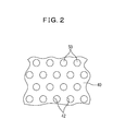
Fig.2 is a top surface explanatory diagram of the LED element with nanocolumns formed by using a pattern of a mask layer. -
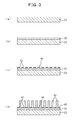
Fig.3 illustrates a process of manufacturing the LED element, includingFig.3a illustrating a state of a substrate,Fig.3b illustrating a state that a buffer layer was grown,Fig.3c illustrating a state that a mask layer was formed, andFig.3d illustrating a state that the nanocolumns were grown. -
Fig.4 illustrates a process of manufacturing the LED element, includingFig.4a illustrating a state that an n-type layer was grown out of a group III nitride semiconductor layer,Fig.4b illustrating a state that the group III nitride semiconductor layer was grown entirely, andFig.4c illustrating a state that the group III nitride semiconductor layer was partially etched. -
Fig.5 is a flowchart illustrating a process of manufacturing the LED element. -
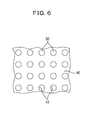
Fig.6 is a top surface explanatory diagram illustrating a modified example of the LED element with the nanocolumns formed by using a pattern of the mask layer. -
Fig.1 to Fig.5 illustrate one embodiment of the present invention andFig.1 is a schematic cross sectional view of an LED element. - As shown in
Fig.1 , an LED element 1 serving as a group III nitride semiconductor device is provided with a group IIInitride semiconductor layer 10 which is expressed by AlxGayIn1-x-yN (0 ≥ x 1, 0 ≤ y ≤ 1, x + y ≤ 1) and asubstrate 20 whose thermal expansion coefficient is less than that of the group IIInitride semiconductor layer 10. In the present embodiment, thesubstrate 20 is made of single crystal 6H-type SiC with a thermal expansion coefficient of 4.2 x 10⁻⁶ /°C. The nitride semiconductor layer serving as a semiconductor light emitting part has a thermal expansion coefficient of 5.6 x 10⁻⁶ /°C. - The
substrate 20 includes donor impurities and acceptor impurities and when it is excited by light emitted from the group IIInitride semiconductor layer 10, light of a predetermined wavelength is emitted by donor-acceptor pair emission. For example, when a bulk SiC substrate is used with donor impurities of N and acceptor impurities of B, excitation by ultraviolet light causes emission of visible light which is roughly yellow to orange. Also, in the case of using a bulk SiC substrate with donor impurities of N and acceptor impurities of Al, excitation by ultraviolet light causes emission of visible light which is roughly blue. Note that any changes can be made for the wavelength of light emitted from the substrate such that visible light of pure white can be obtained by simultaneously adding B and Al as acceptor impurities while maintaining donor impurities of N or the wavelength of emitted light can be shifted to a short wavelength by forming SiC porously. - A
buffer layer 30 made of a group III nitride semiconductor is formed on thesubstrate 20. Thebuffer layer 30 is made of a material which is expressed by a formula of AlxGayIn1-x-yN (0 ≤ x ≤1, 0 ≤ y ≤ 1, x + y ≤ 1). In the present embodiment, for thebuffer layer 30, abuffer layer 30 which is expressed by a formula of AlxGa1-xN (0 < x ≤1) and includes Al is used. - A
mask layer 40 made of an amorphous material is formed on thebuffer layer 30. Apattern 42 for formation ofnanocolumns 50 to be described later is formed in themask layer 40. In the present embodiment, SiO2 is used for themask layer 40. Note that, needless to say, other materials such as SiNx (0 < x) may also be used for themask layer 40. Further, materials such as Al2O3 and W can also be used for themask layer 40. These materials may be either polycrystalline or amorphous. - As shown in
Fig.2 , thepattern 42 of themask layer 40 is formed such thatcircular holes 44 are arranged at intersection points in an equilateral triangular lattice. Theholes 44 which may have any diameters and intervals can be arranged with, for example, a diameter of each of theholes 44 in a range of 50 to 1000 nm and an interval between theholes 44 adjacent to each other in a range of 100 to 1000 nm. - The
nanocolumns 50 are grown through thepattern 42 of themask layer 40 via thebuffer 30. In the present embodiment, GaN is used for thenanocolumns 50. Thenanocolumns 50 are grown corresponding to thepattern 42 so that dislocation density is made smaller than the case of growing them without themask layer 40. In the present embodiment, thenanocolumns 50 can be formed into a cylindrical shape with an aspect ratio of 1 or more. Note that thenanocolumns 50 may be formed into any shapes other than a cylindrical shape as long as being formed into a columnar shape. - The group III
nitride semiconductor layer 10 is formed on themask layer 40. The group IIInitride semiconductor layer 10 includes an n-type layer 12, a multiple quantum wellactive layer 14, a p-type cladding layer 16 and a p-type contact layer 18 to be formed from thesubstrate 20 side in this order. The group IIInitride semiconductor layer 10 is partially removed by etching to partially expose the n-type layer 12 and the exposed area is used for arranging an n-side electrode 60. A p-side electrode 62 is also formed on the p-type contact layer 18. - In the present embodiment, the n-
type layer 12 is formed of n-GaN obtained by doping a predetermined amount of n-type dopant (e.g. Si). The multiple quantum wellactive layer 14 also has a multiple quantum well structure formed by InxGa1-xN (0 ≤ x ≤ 1) / AlyGa1-yN (0 ≤ y ≤ 1). Furthermore, each of the p-type cladding layer 16 and the p-type contact layer 18 is formed by p-GaN obtained by doping a predetermined amount of p-type dopant (e.g. Mg). - Layers from the n-
type layer 12 to the p-type contact layer 18 are formed by epitaxial growth of a group III nitride semiconductor. Note that any layer structures can be employed in the group IIInitride semiconductor layer 10 as long as including at least a first conductive layer, an active layer and a second conductive layer and allowing the active layer to emit light by recombined electrons and positive holes in response to voltage application to the first conductive layer and the second conductive layer. - The n-
side electrode 60 which is formed on the n-type layer 12 is made of, for example, Ni-Au and formed by the vacuum deposition method, sputtering method and CVD (Chemical Vapor Deposition) method or other methods. The p-side electrode 62 which is formed on the p-type contact layer 18 is made of, for example, ITO (Indium Tin Oxide) and formed by the vacuum deposition method, sputtering method and CVD (Chemical Vapor Deposition) method or other methods. - Next, a method for manufacturing the LED element 1 will be explained with reference to
Fig.3 to Fig.5 .Fig.3 andFig.4 are a schematic cross sectional view of the LED element andFig.5 is a flowchart of the method for manufacturing the LED element. Note that the LED element is illustrated by the unit of one element inFig.3 andFig.4 so as to correspond toFig.1 for explanation, but it is actually provided in a wafer state before element separation and other elements are formed continuously to the left and right thereof. - Firstly, single crystal 6H-type SiC is generated in a bulk state containing donor impurities and acceptor impurities that were doped by the sublimation method. Note that doping concentration of impurities in the SiC crystal can be controlled by adding impurity gas to atmospheric gas and adding an impurity element or a compound thereof to base powder at the growth of the crystal. As shown in
Fig.3a , thesubstrate 20 is fabricated by creating a bulk crystal of, for example, about 30 mm resulting from bulk growth by the sublimation method and passing through processes such as outer periphery grinding, slicing, surface grinding and surface polishing. Here, thesubstrate 20 which may have any thicknesses is set to have a thickness of, for example, 250 µm. - Thereafter, as shown in
Fig.3b , thebuffer layer 30 is grown epitaxially on the surface 20 (i.e. buffer layer formation process S10 inFig.5 ). In the present embodiment, thebuffer layer 30 is formed to cover the entire surface on thesubstrate 20 by the sputtering method. Note that thebuffer layer 30 can also be formed by the MOCVD (Metal Organic Chemical Vapor Deposition) method, the MBE (Molecular Beam Epitaxy) method and the HVPE (Halide Vapor Phase Epitaxy) method or other methods. In addition, thebuffer layer 30 can also be formed by the laser ablation method. Here, thebuffer layer 30 which may have any thicknesses is set to have a thickness of, for example, 10 to 200 nm. - Next, as shown in
Fig.3c , themask layer 40 is formed above thesubstrate 20 on which thebuffer layer 30 was formed (i.e. mask layer formation process S20 inFig.5 ). In the present embodiment, themask layer 40 is formed to cover the entire surface on thebuffer layer 30 by the vacuum deposition method. Here, themask layer 40 which may have any thicknesses is set to have a thickness of, for example, 10 to 200 nm. With the thickness of this level, effects of inhibiting transmission of light emitted from an active layer by themask layer 40 will be small. Moreover, if light is extracted by using the action of interference of light, it is unnecessary to take the above inhibiting effects into consideration and therefore themask layer 40 may be set to be thick enough to achieve the action of interference. Thereafter, thepattern 44 is formed in themask layer 40 by using the nanoimprint technique. - Then, as shown in
Fig.3d , thepattern 42 of themask layer 40 is used to grow thenanocolumns 50 epitaxially (i.e. nanocolumn growth process S30 inFig.5 ). In the present embodiment, thepattern 42 of themask layer 40 is used to selectively grow thenanocolumns 50 on thebuffer layer 30 by the MOCVD method. Note that, needless to say, the MBE method and the HVPE method or other methods may also be used to grow thenanocolumns 50. Thenanocolumns 50 which may have any heights are set to have a height of, for example, 500 nm. In the present embodiment, thenanocolumns 50 are selectively grown above thesubstrate 20, whereby dislocation density in thenanocolumns 50 is extremely small in comparison with a case of growing a semiconductor layer to cover the entire surface on thesubstrate 20. - When formation of the
nanocolumns 50 is completed, the group IIInitride semiconductor layer 10 is grown (i.e. semiconductor layer growth process inFig.5 ). In the present embodiment, thenanocolumns 50 and the group IIInitride semiconductor layer 10 are grown continuously in the MOCVD device. Here, the V/III ratio is preferably smaller in the nanocolumn growth process than in the semiconductor growth process. For example, the V/III ratio can be less than 900 in the nanocolumn growth process. If the V/III ratio is too large at the growth of the nanocolumns, a semiconductor which is to be grown cannot be formed into a columnar shape. It is also preferable to supply a smaller amount of gallium in the nanocolumn growth process than in the semiconductor layer growth process. If a supply amount of gallium is too large in the nanocolumn growth process, a semiconductor may be grown into crystals in an island state on the mask to be integrated with the nanocolumns or the nanocolumns may have various shapes. - In the present embodiment, after formation of the n-
type layer 12 so as to fill in thenanocolumns 50 as shown inFig.4a , the multiple quantum wellactive layer 14, the p-type cladding layer 16 and the p-type contact layer 18 are grown sequentially from themask layer 40 side as shown inFig.4b . At this time, in the group IIInitride semiconductor layer 10 which is grown on themask layer 40, dislocation occurring in the inside is terminated in an area to be in contact with sidewalls of thenanocolumns 50, whereby dislocation density can be reduced. Also, owing to low dislocation density in thenanocolumns 50 themselves, dislocation propagated from thenanocolumns 50 is extremely rare. - In addition, because the nanocolumns 50 and the group III
nitride semiconductor layer 10 are formed continuously by the MOCVD device after formation of thebuffer layer 30 by a sputtering device, the manufacturing process can be shortened in comparison with a case of growing thebuffer layer 30 by the MOCVD device. Therefore, manufacturing costs of the light emitting element 1 can be reduced. - Moreover, owing to absence of a mask layer formation process interposed between the nanocolumn growth process and the semiconductor layer growth process, the group III
nitride semiconductor layer 10 of a good quality can be obtained. If themask layer 40 which is amorphous is formed after formation of thenanocolumns 50 made of a group III nitride semiconductor, the surface of thenanocolumns 50 is deteriorated by the components of themask layer 40 and the deterioratednanocolumns 50 are used as a seed to grow the group IIInitride semiconductor layer 10, wherein the group IIInitride semiconductor layer 10 of a good quality is difficult to obtain. - Furthermore, the
mask layer 40 made of an amorphous material prevents the group IIInitride semiconductor layer 10 formed on themask layer 40 from being firmly connected to themask layer 40. Therefore, if excessive stress occurs between the group IIInitride semiconductor layer 10 and themask layer 40, relative slippage of the group IIInitride semiconductor layer 10 and themask layer 40 is permissible. This will also contribute to reduction of dislocation density in the group IIInitride semiconductor layer 10. - Note that each of layers in the group III
nitride semiconductor layer 10 may have any thicknesses but can also be set such that, for example, the n-type layer 12 has a thickness of 3 µm, the multiple quantum wellactive layer 14 has a thickness of 100 nm, the p-type cladding layer 16 has a thickness of 80 nm, and the p-type contact layer 18 has a thickness of 10 nm. Thus, the group IIInitride semiconductor layer 10 can be set to have a thickness of 3 µm or more. After the growth of the group IIInitride semiconductor layer 10, a mask made of photoresist is formed on the p-type contact layer 18 by using the photolithography technique and etching is made from the p-type contact layer 18 to the surface of the n-type layer 12, after which the mask is removed (i.e. etching process S50 inFig.5 ). Therefore, a mesa part composed of a plurality of compound semiconductor layers including the n-type layer 12 to the p-type contact layer 18 is formed as shown inFig.4c - Then, the vacuum deposition method and the photolithography technique are used to form the n-
side electrode 60 and the p-side electrode 62 (i.e. electrode formation process S60 inFig.5 ). Although the present embodiment uses different materials for the n-side electrode 60 and the p-side electrode 62, the n-side electrode 40 and the p-side electrode 62 can be formed simultaneously by using the same material. Note that a heat treatment can be applied at a predetermined temperature under a predetermined atmosphere for a predetermined period of time in order to ensure ohmic contact and adhesiveness between each of theelectrodes nitride semiconductor layer 10. Thereafter, the completed device is divided into a plurality of the LED elements 1 by dicing and thus the LED element 1 is manufactured. - In the LED element 1 which is structured as stated above, ultraviolet light is emitted from the multiple quantum well
active layer 14 in response to voltage application to the p-side electrode 62 and the n-side electrode 60. Then, ultraviolet light is converted into visible light by thesubstrate 20 and emitted to the outside. - According to the LED element 1, the
nanocolumns 50 are selectively grown through themask layer 40 and therefore reduction of dislocation density in thenanocolumns 50 themselves can be achieved. As a result, dislocation propagated from thenanocolumns 50 to the group IIInitride semiconductor layer 10 formed on themask layer 40 is significantly reduced to achieve reduction of dislocation density in the group IIInitride semiconductor layer 10. Dislocation which occurred in the group IIInitride semiconductor layer 10 at the growth of the group IIInitride semiconductor layer 10 is terminated at the interface to thenanocolumns 50 and therefore not propagated upward. Accordingly, reduction of dislocation density in the groupIII nitride semiconductor 10 can be precisely achieved. - Also, according to the LED element 1, the
buffer layer 30 which includes Al prevents the group III nitride semiconductor and the substrate from fiercely reacting to each other at the interface therebetween as observed when, for example, GaN is grown directly on a substrate made of SiC or Si, so that the group IIInitride semiconductor layer 10 can be precisely grown on thesubstrate 20. - Moreover, according to the method for manufacturing the LED element 1, the
nanocolumns 50 can be grown by using themask layer 40 which was formed on thesubstrate 20 and the group IIInitride semiconductor layer 10 can also be grown on themask layer 40 as it is. Accordingly, a mask layer removal process which has been carried out in the conventional method is unnecessary and therefore reduction of manufacturing costs can be achieved. - Furthermore, owing to formation of the
buffer layer 30 and thenanocolumns 50 by the sputtering method, a growth process at a low temperature becomes possible to improve mass productivity. In addition, the buffer layer can be formed into a crystal structure of good quality with fewer defects than that formed by the MOCVD method or other methods. - Note that the present invention, which was applied to the LED element 1 serving as a semiconductor device in the example shown in the above embodiment, is also applicable to other devices such as, for example, LD element. Applicable devices include, for example, electronic devices such as field effect transistors and bipolar transistors and solar cells or the like.
- Although the
nanocolumns 50 are arranged at intersection points in a triangular lattice according to the above embodiment, any changes can be made for the arrangement of the nanocolumns and, for example, arrangement at intersection points in a square lattice as shown inFig.6 may also be applied. - In addition, even though the present embodiment uses 6H-type SiC for the
substrate 20, 4H-type Sic or 15R-type SiC may also be used as a matter of course and Si may also be used for thesubstrate 20. Furthermore, thesubstrate 20 may not need to have a fluorescence function and light of any colors may be emitted from the group IIInitride semiconductor layer 10. - Although the embodiment of the present invention is as explained above, the embodiment described above does not limit the invention relating to the scope of claims. It should also be noted that entire combinations of features explained in the embodiment are not necessarily essential to the means for solving the problem in the invention.
-
- 1
- LED ELEMENT
- 10
- GROUP III NITRIDE SEMICONDUCTOR LAYER
- 12
- n-TYPE LAYER
- 14
- MULTIPLE QUANTUM WELL ACTIVE LAYER
- 16
- p-TYPE CLADDING LAYER
- 18
- p-TYPE CONTACT LAYER
- 20
- SUBSTRATE
- 30
- BUFFER LAYER
- 40
- MASK LAYER
- 42
- HOLE
- 44
- PATTERN
- 50
- NANOCOLUMN
- 60
- n-SIDE ELECTRODE
- 62
- p-SIDE ELECTRODE
Claims (5)
- A group III nitride semiconductor device comprising:- a substrate made of SiC or Si;- a mask layer formed on the substrate and including formation of a predetermined pattern;- nanocolumns selectively grown through the predetermined pattern of the mask layer and made of a group III nitride semiconductor; and- a group III nitride semiconductor layer formed on the mask layer and grown to be higher than the nanocolumns.
- The group III nitride semiconductor device according to claim 1, wherein the mask layer is made of an amorphous material.
- The group III nitride semiconductor device according to claim 2, wherein a buffer layer made of a group III nitride semiconductor including Al is interposed between the substrate and the mask layer.
- A method for manufacturing the group III nitride semiconductor device according to any of claims 1 to 3, the method comprising:- a mask layer formation process to form the mask layer on the substrate;- a nanocolumn growth process to selectively grow the nanocolumns made of a group III nitride semiconductor through the pattern of the mask layer; and- a semiconductor layer growth process to grow the group III nitride semiconductor layer on the mask layer.
- The method for manufacturing the group III nitride semiconductor device according to claim 3, the method comprising:- a buffer layer formation process to form the buffer layer on the substrate by the sputtering method;- a mask layer formation process to form the mask layer on the substrate provided with the buffer layer formed thereon;- a nanocolumn growth process to selectively grow the nanocolumns made of a group III nitride semiconductor through the pattern of the mask layer; and- a semiconductor layer growth process to grow the group III nitride semiconductor layer on the mask layer.
Applications Claiming Priority (2)
| Application Number | Priority Date | Filing Date | Title |
|---|---|---|---|
| JP2010273209 | 2010-12-08 | ||
| PCT/JP2011/077240 WO2012077513A1 (en) | 2010-12-08 | 2011-11-25 | Group iii nitride semiconductor device and method for producing same |
Publications (2)
| Publication Number | Publication Date |
|---|---|
| EP2571065A1 true EP2571065A1 (en) | 2013-03-20 |
| EP2571065A4 EP2571065A4 (en) | 2016-03-23 |
Family
ID=46207007
Family Applications (1)
| Application Number | Title | Priority Date | Filing Date |
|---|---|---|---|
| EP11847760.3A Withdrawn EP2571065A4 (en) | 2010-12-08 | 2011-11-25 | Group iii nitride semiconductor device and method for producing same |
Country Status (5)
| Country | Link |
|---|---|
| US (1) | US9142619B2 (en) |
| EP (1) | EP2571065A4 (en) |
| JP (1) | JP5932664B2 (en) |
| CN (1) | CN102959739B (en) |
| WO (1) | WO2012077513A1 (en) |
Cited By (9)
| Publication number | Priority date | Publication date | Assignee | Title |
|---|---|---|---|---|
| EP3131126A4 (en) * | 2014-04-07 | 2017-10-11 | LG Innotek Co., Ltd. | Light emitting device and lighting system having same |
| WO2019206844A1 (en) * | 2018-04-22 | 2019-10-31 | Epinovatech Ab | Reinforced thin-film device |
| WO2020165164A1 (en) * | 2019-02-12 | 2020-08-20 | Osram Opto Semiconductors Gmbh | Optoelectronic component |
| US11316165B2 (en) | 2020-01-24 | 2022-04-26 | Epinovatech Ab | Solid-state battery layer structure and method for producing the same |
| US11634824B2 (en) | 2021-06-09 | 2023-04-25 | Epinovatech Ab | Device for performing electrolysis of water, and a system thereof |
| US11652454B2 (en) | 2020-02-14 | 2023-05-16 | Epinovatech Ab | Monolithic microwave integrated circuit front-end module |
| US11695066B2 (en) | 2019-12-11 | 2023-07-04 | Epinovatech Ab | Semiconductor layer structure |
| WO2023138883A1 (en) * | 2022-01-24 | 2023-07-27 | Ams-Osram International Gmbh | Method for producing a plurality of optoelectronic semiconductor chips, and optoelectronic semiconductor chip |
| US11955972B2 (en) | 2020-03-13 | 2024-04-09 | Epinovatech Ab | Field-programmable gate array device |
Families Citing this family (6)
| Publication number | Priority date | Publication date | Assignee | Title |
|---|---|---|---|---|
| JP2014076928A (en) * | 2012-10-12 | 2014-05-01 | Waseda Univ | Template substrate |
| FR2997551B1 (en) * | 2012-10-26 | 2015-12-25 | Commissariat Energie Atomique | METHOD OF MANUFACTURING SEMICONDUCTOR STRUCTURE AND SEMICONDUCTOR COMPONENT COMPRISING SUCH A STRUCTURE |
| CN103489974B (en) * | 2013-08-30 | 2016-04-20 | 华灿光电股份有限公司 | A kind of GaN base LED epitaxial slice and preparation method thereof |
| CN104638068B (en) * | 2013-11-07 | 2018-08-24 | 上海蓝光科技有限公司 | A kind of substrat structure and preparation method thereof being used for the growth of III-V group-III nitride |
| CN107611004B (en) * | 2017-08-14 | 2020-01-31 | 南京大学 | method for preparing self-supporting GaN substrate material |
| CN112802930B (en) * | 2021-04-15 | 2021-07-06 | 至芯半导体(杭州)有限公司 | Method for manufacturing group III nitride substrate and semiconductor device |
Family Cites Families (17)
| Publication number | Priority date | Publication date | Assignee | Title |
|---|---|---|---|---|
| JPH07273367A (en) * | 1994-04-01 | 1995-10-20 | Mitsubishi Cable Ind Ltd | Manufacture of semiconductor substrate and light-emitting device |
| JP4153455B2 (en) | 2003-11-28 | 2008-09-24 | 学校法人 名城大学 | Phosphor and light emitting diode |
| KR100646696B1 (en) * | 2004-03-10 | 2006-11-23 | 주식회사 실트론 | Nitride semiconductor device and method for manufacturing the same |
| GB2428681B (en) | 2004-03-24 | 2008-10-29 | Meijo University Educational Foundation | Phosphor |
| KR101199254B1 (en) * | 2004-08-31 | 2012-11-09 | 내셔널 유니버시티 오브 싱가포르 | Nanostructures and method of making the same |
| KR100664986B1 (en) | 2004-10-29 | 2007-01-09 | 삼성전기주식회사 | Nitride based semiconductor device using nanorods and method for manufacturing the same |
| JP4525500B2 (en) * | 2005-07-14 | 2010-08-18 | パナソニック電工株式会社 | Semiconductor light emitting element, lighting device using the same, and method for manufacturing semiconductor light emitting element |
| EP1994552B1 (en) | 2006-03-10 | 2020-12-30 | UNM Rainforest Innovations | Two-phase growth of group iii-v nanowires |
| CN101443887B (en) * | 2006-03-10 | 2011-04-20 | Stc.Unm公司 | Pulsed growth of GAN nanowires and applications in group III nitride semiconductor substrate materials and devices |
| GB2436398B (en) * | 2006-03-23 | 2011-08-24 | Univ Bath | Growth method using nanostructure compliant layers and HVPE for producing high quality compound semiconductor materials |
| KR100767284B1 (en) * | 2006-03-27 | 2007-10-17 | 학교법인 포항공과대학교 | ZnO microstructures and the preparation method thereof |
| JP5066825B2 (en) | 2006-03-31 | 2012-11-07 | 新神戸電機株式会社 | Lead acid battery |
| KR101549270B1 (en) * | 2007-01-12 | 2015-09-01 | 큐나노 에이비 | Nitride nanowires and method of producing such |
| GB0702560D0 (en) * | 2007-02-09 | 2007-03-21 | Univ Bath | Production of Semiconductor devices |
| JP5112761B2 (en) * | 2007-06-26 | 2013-01-09 | パナソニック株式会社 | COMPOUND SEMICONDUCTOR ELEMENT, LIGHTING DEVICE USING SAME, AND METHOD FOR PRODUCING COMPOUND SEMICONDUCTOR ELEMENT |
| JP5097460B2 (en) * | 2007-06-26 | 2012-12-12 | パナソニック株式会社 | COMPOUND SEMICONDUCTOR ELEMENT, LIGHTING DEVICE USING SAME, AND METHOD FOR PRODUCING COMPOUND SEMICONDUCTOR ELEMENT |
| JP5161759B2 (en) * | 2008-12-26 | 2013-03-13 | 富士通株式会社 | Method for manufacturing compound semiconductor device |
-
2011
- 2011-11-25 US US13/704,963 patent/US9142619B2/en not_active Expired - Fee Related
- 2011-11-25 WO PCT/JP2011/077240 patent/WO2012077513A1/en active Application Filing
- 2011-11-25 EP EP11847760.3A patent/EP2571065A4/en not_active Withdrawn
- 2011-11-25 CN CN201180031709.2A patent/CN102959739B/en not_active Expired - Fee Related
- 2011-11-25 JP JP2012547783A patent/JP5932664B2/en not_active Expired - Fee Related
Cited By (13)
| Publication number | Priority date | Publication date | Assignee | Title |
|---|---|---|---|---|
| US9911901B2 (en) | 2014-04-07 | 2018-03-06 | Lg Innotek Co., Ltd. | Light emitting device having buffer layer with graded composition |
| EP3131126A4 (en) * | 2014-04-07 | 2017-10-11 | LG Innotek Co., Ltd. | Light emitting device and lighting system having same |
| EP4053880A1 (en) * | 2018-04-22 | 2022-09-07 | Epinovatech AB | Reinforced thin-film device |
| WO2019206844A1 (en) * | 2018-04-22 | 2019-10-31 | Epinovatech Ab | Reinforced thin-film device |
| CN112020762A (en) * | 2018-04-22 | 2020-12-01 | 艾普诺瓦泰克公司 | Enhanced thin film device |
| US11469300B2 (en) | 2018-04-22 | 2022-10-11 | Epinovatech Ab | Reinforced thin-film semiconductor device and methods of making same |
| WO2020165164A1 (en) * | 2019-02-12 | 2020-08-20 | Osram Opto Semiconductors Gmbh | Optoelectronic component |
| US11695066B2 (en) | 2019-12-11 | 2023-07-04 | Epinovatech Ab | Semiconductor layer structure |
| US11316165B2 (en) | 2020-01-24 | 2022-04-26 | Epinovatech Ab | Solid-state battery layer structure and method for producing the same |
| US11652454B2 (en) | 2020-02-14 | 2023-05-16 | Epinovatech Ab | Monolithic microwave integrated circuit front-end module |
| US11955972B2 (en) | 2020-03-13 | 2024-04-09 | Epinovatech Ab | Field-programmable gate array device |
| US11634824B2 (en) | 2021-06-09 | 2023-04-25 | Epinovatech Ab | Device for performing electrolysis of water, and a system thereof |
| WO2023138883A1 (en) * | 2022-01-24 | 2023-07-27 | Ams-Osram International Gmbh | Method for producing a plurality of optoelectronic semiconductor chips, and optoelectronic semiconductor chip |
Also Published As
| Publication number | Publication date |
|---|---|
| WO2012077513A1 (en) | 2012-06-14 |
| CN102959739B (en) | 2016-05-18 |
| JPWO2012077513A1 (en) | 2014-05-19 |
| CN102959739A (en) | 2013-03-06 |
| US9142619B2 (en) | 2015-09-22 |
| US20130126907A1 (en) | 2013-05-23 |
| JP5932664B2 (en) | 2016-06-08 |
| EP2571065A4 (en) | 2016-03-23 |
Similar Documents
| Publication | Publication Date | Title |
|---|---|---|
| US9142619B2 (en) | Group III nitride semiconductor device and method for manufacturing the same | |
| EP2017884A2 (en) | Buried contact devices for nitride-based films and manufacture thereof | |
| US20230053144A1 (en) | Red led and method of manufacture | |
| JP4882618B2 (en) | GaN-based semiconductor light emitting diode manufacturing method | |
| WO2007001098A1 (en) | Nanostructure having a nitride-based quantum well and light emitting diode employing the same | |
| US20230290903A1 (en) | Led and method of manufacture | |
| US20100012954A1 (en) | Vertical III-Nitride Light Emitting Diodes on Patterned Substrates with Embedded Bottom Electrodes | |
| KR20120138014A (en) | Fabrication method of semiconductor light emitting device | |
| US20060289891A1 (en) | Electronic and/or optoelectronic devices grown on free-standing GaN substrates with GaN spacer structures | |
| KR100661960B1 (en) | Light emitting diode and manufacturing method thereof | |
| CN115000258A (en) | Epitaxial structure for improving modulation bandwidth of micro LED and preparation method thereof | |
| KR101134493B1 (en) | Light emitting diode and method for fabricating the same | |
| KR100820836B1 (en) | Method for manufacturing light emitting diode | |
| WO2009002073A1 (en) | Method for fabricating semiconductor device | |
| CN101728244A (en) | Method for blocking dislocation defects of semiconductor | |
| KR20110135237A (en) | Semiconductor light emitting diode and method for fabricating the same | |
| JP2008028385A (en) | Semiconductor substrate with less defect, semiconductor light emitting devices and method for fabrication thereof | |
| JP5946333B2 (en) | Group III nitride semiconductor device and manufacturing method thereof | |
| JP4548117B2 (en) | Semiconductor light emitting device manufacturing method, integrated semiconductor light emitting device manufacturing method, image display device manufacturing method, and lighting device manufacturing method | |
| TW202211498A (en) | Led device and method of manufacture | |
| KR20130055976A (en) | Light emitting diode having void layer and method of fabricating the same | |
| KR20150015760A (en) | Template for light emitting device fabricating and method of fabricating ultraviolet light emitting device | |
| CN112802869A (en) | White light LED with adjustable single-chip integrated nitride light-emitting wavelength and preparation method thereof | |
| KR100765722B1 (en) | Light emitting device with nano-rod and method for fabricating the same | |
| KR20080082326A (en) | Light emitting diode and method of fabricating the same |
Legal Events
| Date | Code | Title | Description |
|---|---|---|---|
| PUAI | Public reference made under article 153(3) epc to a published international application that has entered the european phase |
Free format text: ORIGINAL CODE: 0009012 |
|
| 17P | Request for examination filed |
Effective date: 20121210 |
|
| AK | Designated contracting states |
Kind code of ref document: A1 Designated state(s): AL AT BE BG CH CY CZ DE DK EE ES FI FR GB GR HR HU IE IS IT LI LT LU LV MC MK MT NL NO PL PT RO RS SE SI SK SM TR |
|
| DAX | Request for extension of the european patent (deleted) | ||
| RA4 | Supplementary search report drawn up and despatched (corrected) |
Effective date: 20160218 |
|
| RIC1 | Information provided on ipc code assigned before grant |
Ipc: H01L 33/32 20100101ALN20160212BHEP Ipc: H01S 5/343 20060101ALI20160212BHEP Ipc: H01L 21/02 20060101ALI20160212BHEP Ipc: H01L 33/00 20100101AFI20160212BHEP Ipc: H01L 33/20 20100101ALI20160212BHEP Ipc: H01L 33/12 20100101ALN20160212BHEP |
|
| STAA | Information on the status of an ep patent application or granted ep patent |
Free format text: STATUS: THE APPLICATION IS DEEMED TO BE WITHDRAWN |
|
| 18D | Application deemed to be withdrawn |
Effective date: 20160920 |