EP2563105A1 - Printed substrate manufacturing method and printed substrate employing same - Google Patents
Printed substrate manufacturing method and printed substrate employing same Download PDFInfo
- Publication number
- EP2563105A1 EP2563105A1 EP11771803A EP11771803A EP2563105A1 EP 2563105 A1 EP2563105 A1 EP 2563105A1 EP 11771803 A EP11771803 A EP 11771803A EP 11771803 A EP11771803 A EP 11771803A EP 2563105 A1 EP2563105 A1 EP 2563105A1
- Authority
- EP
- European Patent Office
- Prior art keywords
- circuit board
- plating
- mask layer
- pattern
- metal layer
- Prior art date
- Legal status (The legal status is an assumption and is not a legal conclusion. Google has not performed a legal analysis and makes no representation as to the accuracy of the status listed.)
- Granted
Links
Images


Classifications
-
- H—ELECTRICITY
- H05—ELECTRIC TECHNIQUES NOT OTHERWISE PROVIDED FOR
- H05K—PRINTED CIRCUITS; CASINGS OR CONSTRUCTIONAL DETAILS OF ELECTRIC APPARATUS; MANUFACTURE OF ASSEMBLAGES OF ELECTRICAL COMPONENTS
- H05K3/00—Apparatus or processes for manufacturing printed circuits
- H05K3/10—Apparatus or processes for manufacturing printed circuits in which conductive material is applied to the insulating support in such a manner as to form the desired conductive pattern
- H05K3/20—Apparatus or processes for manufacturing printed circuits in which conductive material is applied to the insulating support in such a manner as to form the desired conductive pattern by affixing prefabricated conductor pattern
- H05K3/205—Apparatus or processes for manufacturing printed circuits in which conductive material is applied to the insulating support in such a manner as to form the desired conductive pattern by affixing prefabricated conductor pattern using a pattern electroplated or electroformed on a metallic carrier
-
- H—ELECTRICITY
- H05—ELECTRIC TECHNIQUES NOT OTHERWISE PROVIDED FOR
- H05K—PRINTED CIRCUITS; CASINGS OR CONSTRUCTIONAL DETAILS OF ELECTRIC APPARATUS; MANUFACTURE OF ASSEMBLAGES OF ELECTRICAL COMPONENTS
- H05K3/00—Apparatus or processes for manufacturing printed circuits
- H05K3/10—Apparatus or processes for manufacturing printed circuits in which conductive material is applied to the insulating support in such a manner as to form the desired conductive pattern
- H05K3/18—Apparatus or processes for manufacturing printed circuits in which conductive material is applied to the insulating support in such a manner as to form the desired conductive pattern using precipitation techniques to apply the conductive material
-
- H—ELECTRICITY
- H05—ELECTRIC TECHNIQUES NOT OTHERWISE PROVIDED FOR
- H05K—PRINTED CIRCUITS; CASINGS OR CONSTRUCTIONAL DETAILS OF ELECTRIC APPARATUS; MANUFACTURE OF ASSEMBLAGES OF ELECTRICAL COMPONENTS
- H05K3/00—Apparatus or processes for manufacturing printed circuits
- H05K3/10—Apparatus or processes for manufacturing printed circuits in which conductive material is applied to the insulating support in such a manner as to form the desired conductive pattern
- H05K3/20—Apparatus or processes for manufacturing printed circuits in which conductive material is applied to the insulating support in such a manner as to form the desired conductive pattern by affixing prefabricated conductor pattern
-
- H—ELECTRICITY
- H05—ELECTRIC TECHNIQUES NOT OTHERWISE PROVIDED FOR
- H05K—PRINTED CIRCUITS; CASINGS OR CONSTRUCTIONAL DETAILS OF ELECTRIC APPARATUS; MANUFACTURE OF ASSEMBLAGES OF ELECTRICAL COMPONENTS
- H05K3/00—Apparatus or processes for manufacturing printed circuits
- H05K3/22—Secondary treatment of printed circuits
-
- H—ELECTRICITY
- H05—ELECTRIC TECHNIQUES NOT OTHERWISE PROVIDED FOR
- H05K—PRINTED CIRCUITS; CASINGS OR CONSTRUCTIONAL DETAILS OF ELECTRIC APPARATUS; MANUFACTURE OF ASSEMBLAGES OF ELECTRICAL COMPONENTS
- H05K2201/00—Indexing scheme relating to printed circuits covered by H05K1/00
- H05K2201/03—Conductive materials
- H05K2201/0332—Structure of the conductor
- H05K2201/0364—Conductor shape
- H05K2201/0376—Flush conductors, i.e. flush with the surface of the printed circuit
-
- H—ELECTRICITY
- H05—ELECTRIC TECHNIQUES NOT OTHERWISE PROVIDED FOR
- H05K—PRINTED CIRCUITS; CASINGS OR CONSTRUCTIONAL DETAILS OF ELECTRIC APPARATUS; MANUFACTURE OF ASSEMBLAGES OF ELECTRICAL COMPONENTS
- H05K2201/00—Indexing scheme relating to printed circuits covered by H05K1/00
- H05K2201/09—Shape and layout
- H05K2201/09209—Shape and layout details of conductors
- H05K2201/09654—Shape and layout details of conductors covering at least two types of conductors provided for in H05K2201/09218 - H05K2201/095
- H05K2201/098—Special shape of the cross-section of conductors, e.g. very thick plated conductors
-
- H—ELECTRICITY
- H05—ELECTRIC TECHNIQUES NOT OTHERWISE PROVIDED FOR
- H05K—PRINTED CIRCUITS; CASINGS OR CONSTRUCTIONAL DETAILS OF ELECTRIC APPARATUS; MANUFACTURE OF ASSEMBLAGES OF ELECTRICAL COMPONENTS
- H05K2203/00—Indexing scheme relating to apparatus or processes for manufacturing printed circuits covered by H05K3/00
- H05K2203/01—Tools for processing; Objects used during processing
- H05K2203/0147—Carriers and holders
- H05K2203/0152—Temporary metallic carrier, e.g. for transferring material
-
- H—ELECTRICITY
- H05—ELECTRIC TECHNIQUES NOT OTHERWISE PROVIDED FOR
- H05K—PRINTED CIRCUITS; CASINGS OR CONSTRUCTIONAL DETAILS OF ELECTRIC APPARATUS; MANUFACTURE OF ASSEMBLAGES OF ELECTRICAL COMPONENTS
- H05K2203/00—Indexing scheme relating to apparatus or processes for manufacturing printed circuits covered by H05K3/00
- H05K2203/02—Details related to mechanical or acoustic processing, e.g. drilling, punching, cutting, using ultrasound
- H05K2203/025—Abrading, e.g. grinding or sand blasting
-
- H—ELECTRICITY
- H05—ELECTRIC TECHNIQUES NOT OTHERWISE PROVIDED FOR
- H05K—PRINTED CIRCUITS; CASINGS OR CONSTRUCTIONAL DETAILS OF ELECTRIC APPARATUS; MANUFACTURE OF ASSEMBLAGES OF ELECTRICAL COMPONENTS
- H05K2203/00—Indexing scheme relating to apparatus or processes for manufacturing printed circuits covered by H05K3/00
- H05K2203/15—Position of the PCB during processing
- H05K2203/1572—Processing both sides of a PCB by the same process; Providing a similar arrangement of components on both sides; Making interlayer connections from two sides
-
- H—ELECTRICITY
- H05—ELECTRIC TECHNIQUES NOT OTHERWISE PROVIDED FOR
- H05K—PRINTED CIRCUITS; CASINGS OR CONSTRUCTIONAL DETAILS OF ELECTRIC APPARATUS; MANUFACTURE OF ASSEMBLAGES OF ELECTRICAL COMPONENTS
- H05K3/00—Apparatus or processes for manufacturing printed circuits
- H05K3/22—Secondary treatment of printed circuits
- H05K3/26—Cleaning or polishing of the conductive pattern
Definitions
- the present invention relates to a method of producing a printed circuit board by utilizing a transfer process, and a printed circuit board produced by the method.
- a transfer process has been known in which a circuit board is fabricated by burying a pattern in an insulating base in order to smoothen the surface of the circuit board (see Patent Document 2, for example).
- the transfer process includes the step of joining the pattern of plating and an insulating resin together with pressure applied thereto.
- the present invention provides a method of producing a printed circuit board, whereby electrical characteristics of the circuit board can be stabilized even if an outgrowth is formed, surface flatness of the circuit board can be enhanced, and in the case of forming a thick copper pattern, a resist need not have a height matching the thick copper pattern to be formed, and a printed circuit board produced by the method.
- the present invention provides a method of producing a printed circuit board, comprising: forming a metal layer on a support plate; forming a resist layer on the metal layer; forming a mask layer by removing part of the resist layer to form a groove as an exposed area where a conductive pattern is to be formed; subjecting the exposed area to plating process to form a pattern plating, the pattern plating having a stem as a portion of plating up to a level equal to a height of the mask layer, and a cap as a portion of plating exceeding the height of the mask layer and having an outgrowth lying over a surface of the mask layer, as viewed in cross section of the groove; laminating an insulating base on a conductive circuit board constituted by the support plate, the metal layer and the pattern plating, to form a circuit board intermediate in which the pattern plating is buried in the insulating base; removing the support plate and the metal layer from the circuit board intermediate, to form an exposed surface where the conductive pattern and the insulating base
- the mask layer is removed after the plating process.
- the mask layer is left intact as part of the conductive circuit board when the insulating base is laminated on the conductive circuit board.
- the present invention also provides a printed circuit board produced by the method of claim 1.
- the exposed surface where the pattern plating is exposed is mechanically polished for flattening until the stem is removed, that is, up to a position where the outgrowth is exposed. Accordingly, the coatability of a solder resist used in a subsequent process improves, and also components can be stably mounted. Even if an outgrowth is formed, complexity of the cross-sectional shape of the pattern plating is eliminated by the mechanical polishing, so that the electrical characteristics of the printed circuit board are stabilized. Also, even in the case of forming a thick copper pattern plating, the resist layer (mask layer) need not have a height matching the thick copper pattern plating to be formed, and thus the height of the thick copper pattern plating to be formed can be freely set as desired.
- the remaining portion of the mask layer can be removed without fail by the mechanical polishing. It is therefore possible to reliably avoid a situation where the remaining portion of the mask layer falls off after the lamination, creating what is called a void (loss of resin).
- the mask layer is formed using what is called a permanent resist
- the mask layer is infallibly removed together with the stem by the mechanical polishing. It is therefore possible to prevent the quality of the printed circuit board from being adversely affected by the peeling of the mask layer from the pattern plating.
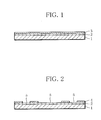
- a metal layer 2 is formed on a support plate 1, and a resist layer 3 is formed on the metal layer 2.
- the support plate 1 is a SUS plate or the like having electrical conductivity and serves as a transfer base.
- the metal layer 2 is a base coating and formed, for example, by electrolytically plating the support plate 1 with copper to a thickness of 12 ⁇ m.
- the resist layer 3 is a dry film or the like. Then, as shown in FIG. 2 , a predetermined portion of the resist layer 3 is removed by using an exposure-development apparatus (not shown) to form a mask layer 4.
- the portion of the resist layer 3 where a conductive pattern is to be formed is removed to form an exposed area (groove) 5 where the surface of the metal layer 2 is exposed.
- the metal layer 2 has the mask layer 4 and the exposed area 5 on its surface.
- the exposed area 5 is subjected to plating process. That is, a pattern plating 6 is formed on the exposed area 5.
- the pattern plating 6 has a stem 7 and a cap 8, as viewed in cross section of the aforementioned groove.
- the stem 7 is a portion of the plating up to a level equal to the height of the mask layer 4, and the cap 8 is a portion of the plating exceeding the height of the mask layer 4. Since the pattern plating 6 is thus formed so as to be higher in level than the mask layer 4, the cap 8 lies over the surface of the mask layer 4.
- a portion of the cap 8 lying over the surface of the mask layer 4 is an outgrowth 8a. Accordingly, the outgrowth 8a forms part of the cap 8.
- the mask layer 4 is removed using a stripping solution or the like, whereupon a conductive circuit board 9 is obtained.
- the conductive circuit board 9 is constituted by the support plate 1, the metal layer 2, and the pattern plating 6. Where a permanent resist is used as the mask layer 4 as mentioned later, however, the mask layer 4 also is an element constituting the conductive circuit board 9.
- FIG. 5 another conductive circuit board 9 and an insulating base 10 are prepared, and the two conductive circuit boards 9 and the insulating base 10 are joined together with application of pressure, as shown in FIG. 6 .
- the figures exemplify the case of fabricating a double-sided circuit board having an electrical conductive pattern formed on both sides thereof.
- the insulating base 10 which is a prepreg or the like, is sandwiched between the two conductive circuit boards 9.
- the conductive circuit boards 9 are placed such that their plated surfaces, namely, the surfaces having the pattern plating 6 formed thereon, face the insulating base 10.
- the conductive circuit boards 9 and the insulating base 10 are joined together with application of pressure and laminated, to obtain a circuit board intermediate 13 shown in FIG. 6 .
- the insulating base 10 is forced in between adjacent coatings of the pattern plating 6 and between the outgrowth 8a and the metal layer 2.
- the pattern plating 6 is buried in the insulating base 10.
- the conductive circuit board 9 is laminated on only one side of the insulating base 10. The double- and single-sided circuit boards fabricated in this manner can of course be used as intermediate and outermost layers of a multilayer circuit board.
- the support plate 1 and the metal layer 2 are removed from the circuit board intermediate 13, so that an electrically conductive pattern 11 and the insulating base 10 are exposed, forming an exposed surface 14.
- the conductive pattern 11 is formed by the exposed surface of the aforementioned stem 7.
- the exposed surface 14 in the illustrated example, the opposite exposed surfaces
- the physical polishing is effected so that the stem 7 may be removed in its entirety, that is, up to a position where the outgrowth 8a is exposed.
- the outgrowth 8a Since the outgrowth 8a is exposed, the line width of the conductive pattern 11 increases. Thus, although the outgrowth 8a is formed, complexity of the cross-sectional shape of the pattern plating 6 is eliminated by the mechanical polishing, so that a produced printed circuit board 12 has stable electrical characteristics. In this manner, according to the present invention, the outgrowth 8a is purposely formed, and therefore, even in the case of forming the copper pattern plating 6 with a large thickness, the resist layer 3 (mask layer 4) need not have a height matching the thick copper pattern plating 6 to be formed, and the height of the copper plating pattern to be formed can be freely set as desired.
- wet polishing using a buffing roll of nonwoven fabric wet polishing using a ceramic buffing roll, wet polishing using an abrasive belt (what is called a belt sander) or the like may be employed.
- the mask layer 4 is removed after the plating process.
- the stripping solution fails to reach the portion of the mask layer 4 interposed between the outgrowth 8a and the metal layer 2, with the result that the mask layer 4 partly remains there.
- the remaining portion of the mask layer 4 can be removed without fail by the aforementioned mechanical polishing. It is therefore possible to reliably avoid a situation where the remaining portion of the mask layer 4 falls off after the lamination, creating what is called a void (loss of resin).
- the mask layer 4 may be left intact as part of the conductive circuit board 9 when the insulating base 10 is laminated on the conductive circuit board 9. Even in such case, the remaining mask layer 4 is infallibly removed together with the stem 7 by the mechanical polishing. It is therefore possible to prevent the quality of the printed circuit board from being adversely affected by the peeling of the mask layer 4 from the pattern plating 6.
Abstract
Description
- The present invention relates to a method of producing a printed circuit board by utilizing a transfer process, and a printed circuit board produced by the method.
- It has been known in the art to remove part of a resist to form an exposed area where a pattern is to be formed. The exposed area is subjected to plating process, and as the plating becomes higher than the height of the resist, it spreads over the resist. That portion of the plating which overlies the resist while exceeding the pattern width set in advance by the resist is called outgrowth. Such outgrowth is disclosed in
Patent Document 1. - Meanwhile, a transfer process has been known in which a circuit board is fabricated by burying a pattern in an insulating base in order to smoothen the surface of the circuit board (see
Patent Document 2, for example). The transfer process includes the step of joining the pattern of plating and an insulating resin together with pressure applied thereto. - However, where a circuit board is fabricated using the transfer process by joining a circuit board intermediate with an outgrowth and an insulating resin together with application of pressure, it is difficult to predict the electrical characteristics of the circuit board because the cross-sectional shape of the pattern plating is complex, with the result that the handleability of the circuit board lowers. In order to prevent the formation of an outgrowth, the height of the resist may be increased. In the case of forming a thick copper plating, however, it is often difficult to form a resist with a height matching the thick copper plating to be formed.
-
- Patent Document 1: Unexamined Japanese Patent Publication No.
5-217755 - Patent Document 2: Unexamined Japanese Patent Publication No.
5-37157 - The present invention provides a method of producing a printed circuit board, whereby electrical characteristics of the circuit board can be stabilized even if an outgrowth is formed, surface flatness of the circuit board can be enhanced, and in the case of forming a thick copper pattern, a resist need not have a height matching the thick copper pattern to be formed, and a printed circuit board produced by the method.
- To achieve the object, the present invention provides a method of producing a printed circuit board, comprising: forming a metal layer on a support plate; forming a resist layer on the metal layer; forming a mask layer by removing part of the resist layer to form a groove as an exposed area where a conductive pattern is to be formed; subjecting the exposed area to plating process to form a pattern plating, the pattern plating having a stem as a portion of plating up to a level equal to a height of the mask layer, and a cap as a portion of plating exceeding the height of the mask layer and having an outgrowth lying over a surface of the mask layer, as viewed in cross section of the groove; laminating an insulating base on a conductive circuit board constituted by the support plate, the metal layer and the pattern plating, to form a circuit board intermediate in which the pattern plating is buried in the insulating base; removing the support plate and the metal layer from the circuit board intermediate, to form an exposed surface where the conductive pattern and the insulating base are exposed; and mechanically polishing the exposed surface until the stem of the pattern plating is removed, to increase a line width of the conductive pattern on the exposed surface to a width greater than that of the groove.
- According to the present invention, in the method of
claim 1, the mask layer is removed after the plating process. - Also, according to the present invention, in the method of
claim 1, the mask layer is left intact as part of the conductive circuit board when the insulating base is laminated on the conductive circuit board. - The present invention also provides a printed circuit board produced by the method of
claim 1. - According to the present invention, the exposed surface where the pattern plating is exposed is mechanically polished for flattening until the stem is removed, that is, up to a position where the outgrowth is exposed. Accordingly, the coatability of a solder resist used in a subsequent process improves, and also components can be stably mounted. Even if an outgrowth is formed, complexity of the cross-sectional shape of the pattern plating is eliminated by the mechanical polishing, so that the electrical characteristics of the printed circuit board are stabilized. Also, even in the case of forming a thick copper pattern plating, the resist layer (mask layer) need not have a height matching the thick copper pattern plating to be formed, and thus the height of the thick copper pattern plating to be formed can be freely set as desired.
- Generally, it is likely that a stripping solution fails to reach the portion of the mask layer interposed between the outgrowth and the metal layer, with the result that the mask layer partly remains there. According to the present invention, the remaining portion of the mask layer can be removed without fail by the mechanical polishing. It is therefore possible to reliably avoid a situation where the remaining portion of the mask layer falls off after the lamination, creating what is called a void (loss of resin).
- According to the present invention, even in the case where the mask layer is formed using what is called a permanent resist, the mask layer is infallibly removed together with the stem by the mechanical polishing. It is therefore possible to prevent the quality of the printed circuit board from being adversely affected by the peeling of the mask layer from the pattern plating.
- According to the present invention, a printed circuit board having the aforementioned advantageous effects can be obtained.
-
-
FIG. 1 schematically illustrates a method of producing a printed circuit board according to the present invention. -
FIG. 2 schematically illustrates the printed circuit board production method of the present invention. -
FIG. 3 schematically illustrates the printed circuit board production method of the present invention. -
FIG. 4 schematically illustrates the printed circuit board production method of the present invention. -
FIG. 5 schematically illustrates the printed circuit board production method of the present invention. -
FIG. 6 schematically illustrates the printed circuit board production method of the present invention. -
FIG. 7 schematically illustrates the printed circuit board production method of the present invention. -
FIG. 8 schematically illustrates the printed circuit board production method of the present invention. - As illustrated in
FIG. 1 , ametal layer 2 is formed on asupport plate 1, and a resist layer 3 is formed on themetal layer 2. Thesupport plate 1 is a SUS plate or the like having electrical conductivity and serves as a transfer base. Themetal layer 2 is a base coating and formed, for example, by electrolytically plating thesupport plate 1 with copper to a thickness of 12 µm. The resist layer 3 is a dry film or the like. Then, as shown inFIG. 2 , a predetermined portion of the resist layer 3 is removed by using an exposure-development apparatus (not shown) to form amask layer 4. Specifically, the portion of the resist layer 3 where a conductive pattern is to be formed is removed to form an exposed area (groove) 5 where the surface of themetal layer 2 is exposed. Thus, themetal layer 2 has themask layer 4 and the exposedarea 5 on its surface. - Subsequently, as illustrated in
FIG. 3 , the exposedarea 5 is subjected to plating process. That is, a pattern plating 6 is formed on the exposedarea 5. Thepattern plating 6 has astem 7 and acap 8, as viewed in cross section of the aforementioned groove. Thestem 7 is a portion of the plating up to a level equal to the height of themask layer 4, and thecap 8 is a portion of the plating exceeding the height of themask layer 4. Since the pattern plating 6 is thus formed so as to be higher in level than themask layer 4, thecap 8 lies over the surface of themask layer 4. A portion of thecap 8 lying over the surface of themask layer 4 is an outgrowth 8a. Accordingly, the outgrowth 8a forms part of thecap 8. Then, as shown inFIG. 4 , themask layer 4 is removed using a stripping solution or the like, whereupon aconductive circuit board 9 is obtained. Specifically, theconductive circuit board 9 is constituted by thesupport plate 1, themetal layer 2, and the pattern plating 6. Where a permanent resist is used as themask layer 4 as mentioned later, however, themask layer 4 also is an element constituting theconductive circuit board 9. - Then, as illustrated in
FIG. 5 , anotherconductive circuit board 9 and aninsulating base 10 are prepared, and the twoconductive circuit boards 9 and theinsulating base 10 are joined together with application of pressure, as shown inFIG. 6 . The figures exemplify the case of fabricating a double-sided circuit board having an electrical conductive pattern formed on both sides thereof. Specifically, theinsulating base 10, which is a prepreg or the like, is sandwiched between the twoconductive circuit boards 9. At this time, theconductive circuit boards 9 are placed such that their plated surfaces, namely, the surfaces having the pattern plating 6 formed thereon, face theinsulating base 10. Theconductive circuit boards 9 and theinsulating base 10 are joined together with application of pressure and laminated, to obtain a circuit board intermediate 13 shown inFIG. 6 . During the lamination, the insulatingbase 10 is forced in between adjacent coatings of the pattern plating 6 and between theoutgrowth 8a and themetal layer 2. As a result, the pattern plating 6 is buried in the insulatingbase 10. In the case of fabricating a single-sided circuit board having a conductive pattern formed on one side thereof, theconductive circuit board 9 is laminated on only one side of the insulatingbase 10. The double- and single-sided circuit boards fabricated in this manner can of course be used as intermediate and outermost layers of a multilayer circuit board. - Subsequently, as illustrated in
FIG. 7 , thesupport plate 1 and themetal layer 2 are removed from the circuit board intermediate 13, so that an electricallyconductive pattern 11 and the insulatingbase 10 are exposed, forming an exposedsurface 14. Theconductive pattern 11 is formed by the exposed surface of theaforementioned stem 7. Then, as shown inFIG. 8 , the exposed surface 14 (in the illustrated example, the opposite exposed surfaces) is mechanically polished to be flattened. This makes it possible to improve the coatability of a solder resist used in a subsequent process, and also to stabilize the mounting of components. The physical polishing (mechanical polishing) is effected so that thestem 7 may be removed in its entirety, that is, up to a position where theoutgrowth 8a is exposed. Since theoutgrowth 8a is exposed, the line width of theconductive pattern 11 increases. Thus, although theoutgrowth 8a is formed, complexity of the cross-sectional shape of the pattern plating 6 is eliminated by the mechanical polishing, so that a produced printedcircuit board 12 has stable electrical characteristics. In this manner, according to the present invention, theoutgrowth 8a is purposely formed, and therefore, even in the case of forming the copper pattern plating 6 with a large thickness, the resist layer 3 (mask layer 4) need not have a height matching the thick copper pattern plating 6 to be formed, and the height of the copper plating pattern to be formed can be freely set as desired. - For the mechanical polishing, wet polishing using a buffing roll of nonwoven fabric, wet polishing using a ceramic buffing roll, wet polishing using an abrasive belt (what is called a belt sander) or the like may be employed.
- In the aforementioned example, the
mask layer 4 is removed after the plating process. Generally, it is likely that the stripping solution fails to reach the portion of themask layer 4 interposed between theoutgrowth 8a and themetal layer 2, with the result that themask layer 4 partly remains there. The remaining portion of themask layer 4 can be removed without fail by the aforementioned mechanical polishing. It is therefore possible to reliably avoid a situation where the remaining portion of themask layer 4 falls off after the lamination, creating what is called a void (loss of resin). - Where a permanent resist is used as the
mask layer 4 as stated above, themask layer 4 may be left intact as part of theconductive circuit board 9 when the insulatingbase 10 is laminated on theconductive circuit board 9. Even in such case, the remainingmask layer 4 is infallibly removed together with thestem 7 by the mechanical polishing. It is therefore possible to prevent the quality of the printed circuit board from being adversely affected by the peeling of themask layer 4 from the pattern plating 6. -
- 1
- support plate
- 2
- metal layer
- 3
- resist layer
- 4
- mask layer
- 5
- exposed area
- 6
- pattern plating
- 7
- stem
- 8
- cap
- 8a
- outgrowth
- 9
- conductive circuit board
- 10
- insulating base
- 11
- pattern
- 12
- printed circuit board
- 13
- circuit board intermediate
- 14
- exposed surface
Claims (4)
- A method of producing a printed circuit board, comprising:forming a metal layer on a support plate;forming a resist layer on the metal layer;forming a mask layer by removing part of the resist layer to form a groove as an exposed area where a conductive pattern is to be formed;subjecting the exposed area to plating process to form a pattern plating, the pattern plating having a stem as a portion of plating up to a level equal to a height of the mask layer, and a cap as a portion of plating exceeding the height of the mask layer and having an outgrowth lying over a surface of the mask layer, as viewed in cross section of the groove;laminating an insulating base on a conductive circuit board constituted by the support plate, the metal layer and the pattern plating, to form a circuit board intermediate in which the pattern plating is buried in the insulating base;removing the support plate and the metal layer from the circuit board intermediate, to form an exposed surface where the conductive pattern and the insulating base are exposed; andmechanically polishing the exposed surface until the stem of the pattern plating is removed, to increase a line width of the conductive pattern on the exposed surface to a width greater than that of the groove.
- The method according to claim 1, wherein the mask layer is removed after the plating process.
- The method according to claim 1, wherein the mask layer is left intact as part of the conductive circuit board when the insulating base is laminated on the conductive circuit board.
- A printed circuit board produced by the method according to claim 1.
Applications Claiming Priority (2)
| Application Number | Priority Date | Filing Date | Title |
|---|---|---|---|
| JP2010099519A JP4896247B2 (en) | 2010-04-23 | 2010-04-23 | Printed circuit board manufacturing method and printed circuit board using the same |
| PCT/JP2011/054724 WO2011132463A1 (en) | 2010-04-23 | 2011-03-02 | Printed substrate manufacturing method and printed substrate employing same |
Publications (3)
| Publication Number | Publication Date |
|---|---|
| EP2563105A1 true EP2563105A1 (en) | 2013-02-27 |
| EP2563105A4 EP2563105A4 (en) | 2015-01-28 |
| EP2563105B1 EP2563105B1 (en) | 2016-07-20 |
Family
ID=44834002
Family Applications (1)
| Application Number | Title | Priority Date | Filing Date |
|---|---|---|---|
| EP11771803.1A Not-in-force EP2563105B1 (en) | 2010-04-23 | 2011-03-02 | Printed substrate manufacturing method and printed substrate employing same |
Country Status (7)
| Country | Link |
|---|---|
| US (1) | US9185811B2 (en) |
| EP (1) | EP2563105B1 (en) |
| JP (1) | JP4896247B2 (en) |
| KR (1) | KR101352819B1 (en) |
| CN (1) | CN102870510B (en) |
| TW (1) | TWI422297B (en) |
| WO (1) | WO2011132463A1 (en) |
Families Citing this family (8)
| Publication number | Priority date | Publication date | Assignee | Title |
|---|---|---|---|---|
| JP4896247B2 (en) * | 2010-04-23 | 2012-03-14 | 株式会社メイコー | Printed circuit board manufacturing method and printed circuit board using the same |
| WO2014119178A1 (en) * | 2013-01-30 | 2014-08-07 | 京セラ株式会社 | Method for producing mounted structure |
| TWI517775B (en) * | 2014-03-06 | 2016-01-11 | 相互股份有限公司 | Printed circuit board and method thereof |
| TWI566309B (en) * | 2016-01-08 | 2017-01-11 | 恆勁科技股份有限公司 | Method of fabricating package substrates |
| CN108401361B (en) * | 2017-02-04 | 2020-08-07 | 欣兴电子股份有限公司 | Circuit board and manufacturing method thereof |
| US10512165B2 (en) | 2017-03-23 | 2019-12-17 | Unimicron Technology Corp. | Method for manufacturing a circuit board |
| CN108958876B (en) * | 2018-07-23 | 2022-02-01 | 郑州云海信息技术有限公司 | Display method and device of browser page |
| CN112165773B (en) * | 2020-10-07 | 2022-10-11 | 广州添利电子科技有限公司 | Process for manufacturing graph in circuit burying mode |
Citations (3)
| Publication number | Priority date | Publication date | Assignee | Title |
|---|---|---|---|---|
| GB1023873A (en) * | 1962-06-11 | 1966-03-30 | Rca Corp | Insulating ferrite articles with embedded conductors and method of making same |
| EP0545328A2 (en) * | 1991-11-29 | 1993-06-09 | Hitachi Chemical Co., Ltd. | Printed circuit board manufacturing process |
| US5369881A (en) * | 1992-09-25 | 1994-12-06 | Nippon Mektron, Ltd. | Method of forming circuit wiring pattern |
Family Cites Families (18)
| Publication number | Priority date | Publication date | Assignee | Title |
|---|---|---|---|---|
| JPS60147192A (en) * | 1984-01-11 | 1985-08-03 | 株式会社日立製作所 | Method of producing printed circuit board |
| US5197184A (en) * | 1990-09-11 | 1993-03-30 | Hughes Aircraft Company | Method of forming three-dimensional circuitry |
| JPH0537157A (en) | 1991-07-31 | 1993-02-12 | Sony Corp | Manufacture of multilayer printed circuit board |
| JPH05217755A (en) | 1992-02-05 | 1993-08-27 | Tokai Rubber Ind Ltd | Manufacture of pattern plating molded product |
| US5358604A (en) * | 1992-09-29 | 1994-10-25 | Microelectronics And Computer Technology Corp. | Method for producing conductive patterns |
| JPH08181415A (en) * | 1994-12-27 | 1996-07-12 | Tokai Rubber Ind Ltd | Manufacture of bored circuit substrate |
| US6143116A (en) * | 1996-09-26 | 2000-11-07 | Kyocera Corporation | Process for producing a multi-layer wiring board |
| US6871396B2 (en) * | 2000-02-09 | 2005-03-29 | Matsushita Electric Industrial Co., Ltd. | Transfer material for wiring substrate |
| US6692816B2 (en) * | 2001-11-28 | 2004-02-17 | 3M Innovative Properties Company | Abrasion resistant electrode and device |
| WO2004014114A1 (en) * | 2002-07-31 | 2004-02-12 | Sony Corporation | Method for manufacturing board with built-in device and board with built-in device, and method for manufacturing printed wiring board and printed wiring board |
| US6898850B2 (en) | 2002-08-06 | 2005-05-31 | Matsushita Electric Industrial Co., Ltd. | Method of manufacturing circuit board and communication appliance |
| KR100607626B1 (en) * | 2004-05-25 | 2006-08-01 | 대덕전자 주식회사 | Flat coating process with utilizing a resin coated copper for printed circuit board |
| JP2006339365A (en) * | 2005-06-01 | 2006-12-14 | Mitsui Mining & Smelting Co Ltd | Wiring board, its manufacturing method, manufacturing method of multilayer laminated wiring board and forming method of via hole |
| JP2007250925A (en) * | 2006-03-17 | 2007-09-27 | Ricoh Co Ltd | Wiring structure and its method for manufacturing |
| JP2008098563A (en) * | 2006-10-16 | 2008-04-24 | Seiko Epson Corp | Element substrate and its manufacturing method |
| JP4697156B2 (en) * | 2007-02-28 | 2011-06-08 | トヨタ自動車株式会社 | Circuit board manufacturing method |
| US8033014B2 (en) * | 2008-07-07 | 2011-10-11 | Unimicron Technology Corp. | Method of making a molded interconnect device |
| JP4896247B2 (en) * | 2010-04-23 | 2012-03-14 | 株式会社メイコー | Printed circuit board manufacturing method and printed circuit board using the same |
-
2010
- 2010-04-23 JP JP2010099519A patent/JP4896247B2/en not_active Expired - Fee Related
-
2011
- 2011-03-02 WO PCT/JP2011/054724 patent/WO2011132463A1/en active Application Filing
- 2011-03-02 US US13/642,471 patent/US9185811B2/en not_active Expired - Fee Related
- 2011-03-02 EP EP11771803.1A patent/EP2563105B1/en not_active Not-in-force
- 2011-03-02 KR KR1020127026339A patent/KR101352819B1/en not_active IP Right Cessation
- 2011-03-02 CN CN201180020204.6A patent/CN102870510B/en not_active Expired - Fee Related
- 2011-03-18 TW TW100109347A patent/TWI422297B/en not_active IP Right Cessation
Patent Citations (3)
| Publication number | Priority date | Publication date | Assignee | Title |
|---|---|---|---|---|
| GB1023873A (en) * | 1962-06-11 | 1966-03-30 | Rca Corp | Insulating ferrite articles with embedded conductors and method of making same |
| EP0545328A2 (en) * | 1991-11-29 | 1993-06-09 | Hitachi Chemical Co., Ltd. | Printed circuit board manufacturing process |
| US5369881A (en) * | 1992-09-25 | 1994-12-06 | Nippon Mektron, Ltd. | Method of forming circuit wiring pattern |
Non-Patent Citations (1)
| Title |
|---|
| See also references of WO2011132463A1 * |
Also Published As
| Publication number | Publication date |
|---|---|
| US20130043063A1 (en) | 2013-02-21 |
| WO2011132463A1 (en) | 2011-10-27 |
| KR20130064044A (en) | 2013-06-17 |
| TW201212754A (en) | 2012-03-16 |
| CN102870510B (en) | 2014-01-01 |
| JP2011228605A (en) | 2011-11-10 |
| JP4896247B2 (en) | 2012-03-14 |
| US9185811B2 (en) | 2015-11-10 |
| TWI422297B (en) | 2014-01-01 |
| EP2563105A4 (en) | 2015-01-28 |
| EP2563105B1 (en) | 2016-07-20 |
| KR101352819B1 (en) | 2014-01-16 |
| CN102870510A (en) | 2013-01-09 |
Similar Documents
| Publication | Publication Date | Title |
|---|---|---|
| EP2563105B1 (en) | Printed substrate manufacturing method and printed substrate employing same | |
| KR101497192B1 (en) | A printed circuit board comprising embeded electronic component within and a method for manufacturing | |
| US9179553B2 (en) | Method of manufacturing multilayer wiring board | |
| KR100957418B1 (en) | Method for maanufacturig pcb and pcb manufactured using the same | |
| JP4994988B2 (en) | Wiring board manufacturing method | |
| TWI551439B (en) | Liquid crystal polymer film with metal foil, method for producing the same, and multilayer printed wiring board, and manufacturing method thereof | |
| US20140182899A1 (en) | Rigid-flexible printed circuit board and method for manufacturing same | |
| JP5047906B2 (en) | Wiring board manufacturing method | |
| TWI578864B (en) | Base board for built-in parts and method of manufacturing the same | |
| CN104780723A (en) | Method for manufacturing wiring board | |
| KR20180112977A (en) | Printed circuit board and manufacturing method thereof | |
| JP2009206409A (en) | Method for manufacturing wiring substrate | |
| CN210899888U (en) | Multilayer substrate and electronic device | |
| JP2003298212A (en) | Printed wiring board and manufacturing method thereof | |
| JP2011171353A (en) | Method of manufacturing printed board, and printed board using this | |
| JP2015002226A (en) | Multilayer wiring board and method for manufacturing the same | |
| JP5483921B2 (en) | Method for manufacturing printed circuit board | |
| KR100776022B1 (en) | Making method of Printed circuit board | |
| KR101063620B1 (en) | Multilayer printed circuit board and its manufacturing method | |
| JP4637893B2 (en) | Method for forming paste bump on printed circuit board | |
| TWI620481B (en) | Method for manufacturing flexible printed circuit board and intermediate product for manufacturing flexible printed circuit board | |
| KR102480712B1 (en) | Printed circuit board | |
| KR100709896B1 (en) | Multilayer printed circuit board and method of manufacturing the same | |
| JP2007511904A (en) | Multilayer printed circuit board and manufacturing method thereof | |
| KR100556174B1 (en) | Plating method for flexible print circuit board |
Legal Events
| Date | Code | Title | Description |
|---|---|---|---|
| PUAI | Public reference made under article 153(3) epc to a published international application that has entered the european phase |
Free format text: ORIGINAL CODE: 0009012 |
|
| 17P | Request for examination filed |
Effective date: 20121015 |
|
| AK | Designated contracting states |
Kind code of ref document: A1 Designated state(s): AL AT BE BG CH CY CZ DE DK EE ES FI FR GB GR HR HU IE IS IT LI LT LU LV MC MK MT NL NO PL PT RO RS SE SI SK SM TR |
|
| DAX | Request for extension of the european patent (deleted) | ||
| A4 | Supplementary search report drawn up and despatched |
Effective date: 20150107 |
|
| RIC1 | Information provided on ipc code assigned before grant |
Ipc: H05K 3/20 20060101AFI20141219BHEP Ipc: H05K 3/26 20060101ALN20141219BHEP |
|
| REG | Reference to a national code |
Ref country code: DE Ref legal event code: R079 Ref document number: 602011028384 Country of ref document: DE Free format text: PREVIOUS MAIN CLASS: H05K0003260000 Ipc: H05K0003200000 |
|
| RIC1 | Information provided on ipc code assigned before grant |
Ipc: H05K 3/26 20060101ALN20151216BHEP Ipc: H05K 3/20 20060101AFI20151216BHEP |
|
| GRAP | Despatch of communication of intention to grant a patent |
Free format text: ORIGINAL CODE: EPIDOSNIGR1 |
|
| INTG | Intention to grant announced |
Effective date: 20160218 |
|
| GRAS | Grant fee paid |
Free format text: ORIGINAL CODE: EPIDOSNIGR3 |
|
| GRAA | (expected) grant |
Free format text: ORIGINAL CODE: 0009210 |
|
| AK | Designated contracting states |
Kind code of ref document: B1 Designated state(s): AL AT BE BG CH CY CZ DE DK EE ES FI FR GB GR HR HU IE IS IT LI LT LU LV MC MK MT NL NO PL PT RO RS SE SI SK SM TR |
|
| REG | Reference to a national code |
Ref country code: GB Ref legal event code: FG4D |
|
| REG | Reference to a national code |
Ref country code: CH Ref legal event code: EP |
|
| REG | Reference to a national code |
Ref country code: IE Ref legal event code: FG4D |
|
| REG | Reference to a national code |
Ref country code: AT Ref legal event code: REF Ref document number: 814995 Country of ref document: AT Kind code of ref document: T Effective date: 20160815 |
|
| REG | Reference to a national code |
Ref country code: DE Ref legal event code: R096 Ref document number: 602011028384 Country of ref document: DE |
|
| REG | Reference to a national code |
Ref country code: LT Ref legal event code: MG4D |
|
| REG | Reference to a national code |
Ref country code: NL Ref legal event code: MP Effective date: 20160720 |
|
| REG | Reference to a national code |
Ref country code: AT Ref legal event code: MK05 Ref document number: 814995 Country of ref document: AT Kind code of ref document: T Effective date: 20160720 |
|
| PG25 | Lapsed in a contracting state [announced via postgrant information from national office to epo] |
Ref country code: NL Free format text: LAPSE BECAUSE OF FAILURE TO SUBMIT A TRANSLATION OF THE DESCRIPTION OR TO PAY THE FEE WITHIN THE PRESCRIBED TIME-LIMIT Effective date: 20160720 Ref country code: HR Free format text: LAPSE BECAUSE OF FAILURE TO SUBMIT A TRANSLATION OF THE DESCRIPTION OR TO PAY THE FEE WITHIN THE PRESCRIBED TIME-LIMIT Effective date: 20160720 Ref country code: NO Free format text: LAPSE BECAUSE OF FAILURE TO SUBMIT A TRANSLATION OF THE DESCRIPTION OR TO PAY THE FEE WITHIN THE PRESCRIBED TIME-LIMIT Effective date: 20161020 Ref country code: FI Free format text: LAPSE BECAUSE OF FAILURE TO SUBMIT A TRANSLATION OF THE DESCRIPTION OR TO PAY THE FEE WITHIN THE PRESCRIBED TIME-LIMIT Effective date: 20160720 Ref country code: LT Free format text: LAPSE BECAUSE OF FAILURE TO SUBMIT A TRANSLATION OF THE DESCRIPTION OR TO PAY THE FEE WITHIN THE PRESCRIBED TIME-LIMIT Effective date: 20160720 Ref country code: IT Free format text: LAPSE BECAUSE OF FAILURE TO SUBMIT A TRANSLATION OF THE DESCRIPTION OR TO PAY THE FEE WITHIN THE PRESCRIBED TIME-LIMIT Effective date: 20160720 Ref country code: IS Free format text: LAPSE BECAUSE OF FAILURE TO SUBMIT A TRANSLATION OF THE DESCRIPTION OR TO PAY THE FEE WITHIN THE PRESCRIBED TIME-LIMIT Effective date: 20161120 Ref country code: RS Free format text: LAPSE BECAUSE OF FAILURE TO SUBMIT A TRANSLATION OF THE DESCRIPTION OR TO PAY THE FEE WITHIN THE PRESCRIBED TIME-LIMIT Effective date: 20160720 |
|
| PG25 | Lapsed in a contracting state [announced via postgrant information from national office to epo] |
Ref country code: BE Free format text: LAPSE BECAUSE OF FAILURE TO SUBMIT A TRANSLATION OF THE DESCRIPTION OR TO PAY THE FEE WITHIN THE PRESCRIBED TIME-LIMIT Effective date: 20160720 Ref country code: AT Free format text: LAPSE BECAUSE OF FAILURE TO SUBMIT A TRANSLATION OF THE DESCRIPTION OR TO PAY THE FEE WITHIN THE PRESCRIBED TIME-LIMIT Effective date: 20160720 Ref country code: PT Free format text: LAPSE BECAUSE OF FAILURE TO SUBMIT A TRANSLATION OF THE DESCRIPTION OR TO PAY THE FEE WITHIN THE PRESCRIBED TIME-LIMIT Effective date: 20161121 Ref country code: ES Free format text: LAPSE BECAUSE OF FAILURE TO SUBMIT A TRANSLATION OF THE DESCRIPTION OR TO PAY THE FEE WITHIN THE PRESCRIBED TIME-LIMIT Effective date: 20160720 Ref country code: LV Free format text: LAPSE BECAUSE OF FAILURE TO SUBMIT A TRANSLATION OF THE DESCRIPTION OR TO PAY THE FEE WITHIN THE PRESCRIBED TIME-LIMIT Effective date: 20160720 Ref country code: PL Free format text: LAPSE BECAUSE OF FAILURE TO SUBMIT A TRANSLATION OF THE DESCRIPTION OR TO PAY THE FEE WITHIN THE PRESCRIBED TIME-LIMIT Effective date: 20160720 Ref country code: SE Free format text: LAPSE BECAUSE OF FAILURE TO SUBMIT A TRANSLATION OF THE DESCRIPTION OR TO PAY THE FEE WITHIN THE PRESCRIBED TIME-LIMIT Effective date: 20160720 Ref country code: GR Free format text: LAPSE BECAUSE OF FAILURE TO SUBMIT A TRANSLATION OF THE DESCRIPTION OR TO PAY THE FEE WITHIN THE PRESCRIBED TIME-LIMIT Effective date: 20161021 |
|
| REG | Reference to a national code |
Ref country code: DE Ref legal event code: R097 Ref document number: 602011028384 Country of ref document: DE |
|
| PG25 | Lapsed in a contracting state [announced via postgrant information from national office to epo] |
Ref country code: RO Free format text: LAPSE BECAUSE OF FAILURE TO SUBMIT A TRANSLATION OF THE DESCRIPTION OR TO PAY THE FEE WITHIN THE PRESCRIBED TIME-LIMIT Effective date: 20160720 Ref country code: EE Free format text: LAPSE BECAUSE OF FAILURE TO SUBMIT A TRANSLATION OF THE DESCRIPTION OR TO PAY THE FEE WITHIN THE PRESCRIBED TIME-LIMIT Effective date: 20160720 |
|
| PLBE | No opposition filed within time limit |
Free format text: ORIGINAL CODE: 0009261 |
|
| STAA | Information on the status of an ep patent application or granted ep patent |
Free format text: STATUS: NO OPPOSITION FILED WITHIN TIME LIMIT |
|
| PG25 | Lapsed in a contracting state [announced via postgrant information from national office to epo] |
Ref country code: SK Free format text: LAPSE BECAUSE OF FAILURE TO SUBMIT A TRANSLATION OF THE DESCRIPTION OR TO PAY THE FEE WITHIN THE PRESCRIBED TIME-LIMIT Effective date: 20160720 Ref country code: BG Free format text: LAPSE BECAUSE OF FAILURE TO SUBMIT A TRANSLATION OF THE DESCRIPTION OR TO PAY THE FEE WITHIN THE PRESCRIBED TIME-LIMIT Effective date: 20161020 Ref country code: DK Free format text: LAPSE BECAUSE OF FAILURE TO SUBMIT A TRANSLATION OF THE DESCRIPTION OR TO PAY THE FEE WITHIN THE PRESCRIBED TIME-LIMIT Effective date: 20160720 Ref country code: SM Free format text: LAPSE BECAUSE OF FAILURE TO SUBMIT A TRANSLATION OF THE DESCRIPTION OR TO PAY THE FEE WITHIN THE PRESCRIBED TIME-LIMIT Effective date: 20160720 Ref country code: CZ Free format text: LAPSE BECAUSE OF FAILURE TO SUBMIT A TRANSLATION OF THE DESCRIPTION OR TO PAY THE FEE WITHIN THE PRESCRIBED TIME-LIMIT Effective date: 20160720 |
|
| 26N | No opposition filed |
Effective date: 20170421 |
|
| PGFP | Annual fee paid to national office [announced via postgrant information from national office to epo] |
Ref country code: DE Payment date: 20170328 Year of fee payment: 7 |
|
| PG25 | Lapsed in a contracting state [announced via postgrant information from national office to epo] |
Ref country code: SI Free format text: LAPSE BECAUSE OF FAILURE TO SUBMIT A TRANSLATION OF THE DESCRIPTION OR TO PAY THE FEE WITHIN THE PRESCRIBED TIME-LIMIT Effective date: 20160720 |
|
| REG | Reference to a national code |
Ref country code: CH Ref legal event code: PL |
|
| GBPC | Gb: european patent ceased through non-payment of renewal fee |
Effective date: 20170302 |
|
| PG25 | Lapsed in a contracting state [announced via postgrant information from national office to epo] |
Ref country code: MC Free format text: LAPSE BECAUSE OF FAILURE TO SUBMIT A TRANSLATION OF THE DESCRIPTION OR TO PAY THE FEE WITHIN THE PRESCRIBED TIME-LIMIT Effective date: 20160720 |
|
| REG | Reference to a national code |
Ref country code: IE Ref legal event code: MM4A |
|
| REG | Reference to a national code |
Ref country code: FR Ref legal event code: ST Effective date: 20171130 |
|
| PG25 | Lapsed in a contracting state [announced via postgrant information from national office to epo] |
Ref country code: FR Free format text: LAPSE BECAUSE OF NON-PAYMENT OF DUE FEES Effective date: 20170331 Ref country code: LU Free format text: LAPSE BECAUSE OF NON-PAYMENT OF DUE FEES Effective date: 20170302 |
|
| PG25 | Lapsed in a contracting state [announced via postgrant information from national office to epo] |
Ref country code: LI Free format text: LAPSE BECAUSE OF NON-PAYMENT OF DUE FEES Effective date: 20170331 Ref country code: CH Free format text: LAPSE BECAUSE OF NON-PAYMENT OF DUE FEES Effective date: 20170331 Ref country code: IE Free format text: LAPSE BECAUSE OF NON-PAYMENT OF DUE FEES Effective date: 20170302 Ref country code: GB Free format text: LAPSE BECAUSE OF NON-PAYMENT OF DUE FEES Effective date: 20170302 |
|
| PG25 | Lapsed in a contracting state [announced via postgrant information from national office to epo] |
Ref country code: MT Free format text: LAPSE BECAUSE OF NON-PAYMENT OF DUE FEES Effective date: 20170302 |
|
| REG | Reference to a national code |
Ref country code: DE Ref legal event code: R119 Ref document number: 602011028384 Country of ref document: DE |
|
| PG25 | Lapsed in a contracting state [announced via postgrant information from national office to epo] |
Ref country code: AL Free format text: LAPSE BECAUSE OF FAILURE TO SUBMIT A TRANSLATION OF THE DESCRIPTION OR TO PAY THE FEE WITHIN THE PRESCRIBED TIME-LIMIT Effective date: 20160720 |
|
| PG25 | Lapsed in a contracting state [announced via postgrant information from national office to epo] |
Ref country code: DE Free format text: LAPSE BECAUSE OF NON-PAYMENT OF DUE FEES Effective date: 20181002 |
|
| PG25 | Lapsed in a contracting state [announced via postgrant information from national office to epo] |
Ref country code: HU Free format text: LAPSE BECAUSE OF FAILURE TO SUBMIT A TRANSLATION OF THE DESCRIPTION OR TO PAY THE FEE WITHIN THE PRESCRIBED TIME-LIMIT; INVALID AB INITIO Effective date: 20110302 |
|
| PG25 | Lapsed in a contracting state [announced via postgrant information from national office to epo] |
Ref country code: CY Free format text: LAPSE BECAUSE OF NON-PAYMENT OF DUE FEES Effective date: 20160720 |
|
| PG25 | Lapsed in a contracting state [announced via postgrant information from national office to epo] |
Ref country code: MK Free format text: LAPSE BECAUSE OF FAILURE TO SUBMIT A TRANSLATION OF THE DESCRIPTION OR TO PAY THE FEE WITHIN THE PRESCRIBED TIME-LIMIT Effective date: 20160720 |
|
| PG25 | Lapsed in a contracting state [announced via postgrant information from national office to epo] |
Ref country code: TR Free format text: LAPSE BECAUSE OF FAILURE TO SUBMIT A TRANSLATION OF THE DESCRIPTION OR TO PAY THE FEE WITHIN THE PRESCRIBED TIME-LIMIT Effective date: 20160720 |