EP2535960B1 - Verfahren zum Herstellen einer nicht-gemeinsamen Deckschicht auf einer organischen Vorrichtung - Google Patents
Verfahren zum Herstellen einer nicht-gemeinsamen Deckschicht auf einer organischen Vorrichtung Download PDFInfo
- Publication number
- EP2535960B1 EP2535960B1 EP12172237.5A EP12172237A EP2535960B1 EP 2535960 B1 EP2535960 B1 EP 2535960B1 EP 12172237 A EP12172237 A EP 12172237A EP 2535960 B1 EP2535960 B1 EP 2535960B1
- Authority
- EP
- European Patent Office
- Prior art keywords
- oleds
- capping layer
- capping
- optically coupled
- layer
- Prior art date
- Legal status (The legal status is an assumption and is not a legal conclusion. Google has not performed a legal analysis and makes no representation as to the accuracy of the status listed.)
- Active
Links
Images


Classifications
-
- H—ELECTRICITY
- H10—SEMICONDUCTOR DEVICES; ELECTRIC SOLID-STATE DEVICES NOT OTHERWISE PROVIDED FOR
- H10K—ORGANIC ELECTRIC SOLID-STATE DEVICES
- H10K50/00—Organic light-emitting devices
- H10K50/80—Constructional details
- H10K50/84—Passivation; Containers; Encapsulations
- H10K50/844—Encapsulations
-
- H—ELECTRICITY
- H10—SEMICONDUCTOR DEVICES; ELECTRIC SOLID-STATE DEVICES NOT OTHERWISE PROVIDED FOR
- H10K—ORGANIC ELECTRIC SOLID-STATE DEVICES
- H10K59/00—Integrated devices, or assemblies of multiple devices, comprising at least one organic light-emitting element covered by group H10K50/00
- H10K59/30—Devices specially adapted for multicolour light emission
- H10K59/35—Devices specially adapted for multicolour light emission comprising red-green-blue [RGB] subpixels
-
- H—ELECTRICITY
- H10—SEMICONDUCTOR DEVICES; ELECTRIC SOLID-STATE DEVICES NOT OTHERWISE PROVIDED FOR
- H10K—ORGANIC ELECTRIC SOLID-STATE DEVICES
- H10K50/00—Organic light-emitting devices
- H10K50/10—OLEDs or polymer light-emitting diodes [PLED]
- H10K50/11—OLEDs or polymer light-emitting diodes [PLED] characterised by the electroluminescent [EL] layers
- H10K50/125—OLEDs or polymer light-emitting diodes [PLED] characterised by the electroluminescent [EL] layers specially adapted for multicolour light emission, e.g. for emitting white light
-
- H—ELECTRICITY
- H10—SEMICONDUCTOR DEVICES; ELECTRIC SOLID-STATE DEVICES NOT OTHERWISE PROVIDED FOR
- H10K—ORGANIC ELECTRIC SOLID-STATE DEVICES
- H10K50/00—Organic light-emitting devices
- H10K50/80—Constructional details
- H10K50/84—Passivation; Containers; Encapsulations
- H10K50/844—Encapsulations
- H10K50/8445—Encapsulations multilayered coatings having a repetitive structure, e.g. having multiple organic-inorganic bilayers
-
- H—ELECTRICITY
- H10—SEMICONDUCTOR DEVICES; ELECTRIC SOLID-STATE DEVICES NOT OTHERWISE PROVIDED FOR
- H10K—ORGANIC ELECTRIC SOLID-STATE DEVICES
- H10K50/00—Organic light-emitting devices
- H10K50/80—Constructional details
- H10K50/85—Arrangements for extracting light from the devices
-
- H—ELECTRICITY
- H10—SEMICONDUCTOR DEVICES; ELECTRIC SOLID-STATE DEVICES NOT OTHERWISE PROVIDED FOR
- H10K—ORGANIC ELECTRIC SOLID-STATE DEVICES
- H10K50/00—Organic light-emitting devices
- H10K50/80—Constructional details
- H10K50/85—Arrangements for extracting light from the devices
- H10K50/852—Arrangements for extracting light from the devices comprising a resonant cavity structure, e.g. Bragg reflector pair
-
- H—ELECTRICITY
- H10—SEMICONDUCTOR DEVICES; ELECTRIC SOLID-STATE DEVICES NOT OTHERWISE PROVIDED FOR
- H10K—ORGANIC ELECTRIC SOLID-STATE DEVICES
- H10K50/00—Organic light-emitting devices
- H10K50/80—Constructional details
- H10K50/85—Arrangements for extracting light from the devices
- H10K50/858—Arrangements for extracting light from the devices comprising refractive means, e.g. lenses
-
- H—ELECTRICITY
- H10—SEMICONDUCTOR DEVICES; ELECTRIC SOLID-STATE DEVICES NOT OTHERWISE PROVIDED FOR
- H10K—ORGANIC ELECTRIC SOLID-STATE DEVICES
- H10K50/00—Organic light-emitting devices
- H10K50/80—Constructional details
- H10K50/86—Arrangements for improving contrast, e.g. preventing reflection of ambient light
-
- H—ELECTRICITY
- H10—SEMICONDUCTOR DEVICES; ELECTRIC SOLID-STATE DEVICES NOT OTHERWISE PROVIDED FOR
- H10K—ORGANIC ELECTRIC SOLID-STATE DEVICES
- H10K59/00—Integrated devices, or assemblies of multiple devices, comprising at least one organic light-emitting element covered by group H10K50/00
- H10K59/30—Devices specially adapted for multicolour light emission
- H10K59/38—Devices specially adapted for multicolour light emission comprising colour filters or colour changing media [CCM]
-
- H—ELECTRICITY
- H10—SEMICONDUCTOR DEVICES; ELECTRIC SOLID-STATE DEVICES NOT OTHERWISE PROVIDED FOR
- H10K—ORGANIC ELECTRIC SOLID-STATE DEVICES
- H10K59/00—Integrated devices, or assemblies of multiple devices, comprising at least one organic light-emitting element covered by group H10K50/00
- H10K59/80—Constructional details
- H10K59/875—Arrangements for extracting light from the devices
-
- H—ELECTRICITY
- H10—SEMICONDUCTOR DEVICES; ELECTRIC SOLID-STATE DEVICES NOT OTHERWISE PROVIDED FOR
- H10K—ORGANIC ELECTRIC SOLID-STATE DEVICES
- H10K71/00—Manufacture or treatment specially adapted for the organic devices covered by this subclass
-
- H—ELECTRICITY
- H10—SEMICONDUCTOR DEVICES; ELECTRIC SOLID-STATE DEVICES NOT OTHERWISE PROVIDED FOR
- H10K—ORGANIC ELECTRIC SOLID-STATE DEVICES
- H10K2102/00—Constructional details relating to the organic devices covered by this subclass
- H10K2102/301—Details of OLEDs
- H10K2102/302—Details of OLEDs of OLED structures
- H10K2102/3023—Direction of light emission
- H10K2102/3026—Top emission
-
- H—ELECTRICITY
- H10—SEMICONDUCTOR DEVICES; ELECTRIC SOLID-STATE DEVICES NOT OTHERWISE PROVIDED FOR
- H10K—ORGANIC ELECTRIC SOLID-STATE DEVICES
- H10K2102/00—Constructional details relating to the organic devices covered by this subclass
- H10K2102/301—Details of OLEDs
- H10K2102/351—Thickness
-
- H—ELECTRICITY
- H10—SEMICONDUCTOR DEVICES; ELECTRIC SOLID-STATE DEVICES NOT OTHERWISE PROVIDED FOR
- H10K—ORGANIC ELECTRIC SOLID-STATE DEVICES
- H10K59/00—Integrated devices, or assemblies of multiple devices, comprising at least one organic light-emitting element covered by group H10K50/00
- H10K59/80—Constructional details
- H10K59/875—Arrangements for extracting light from the devices
- H10K59/879—Arrangements for extracting light from the devices comprising refractive means, e.g. lenses
Definitions
- Opto-electronic devices that make use of organic materials are becoming increasingly desirable for a number of reasons. Many of the materials used to make such devices are relatively inexpensive, so organic opto-electronic devices have the potential for cost advantages over inorganic devices. In addition, the inherent properties of organic materials, such as their flexibility, may make them well suited for particular applications such as fabrication on a flexible substrate. Examples of organic opto-electronic devices include organic light emitting devices (OLEDs), organic phototransistors, organic photovoltaic cells, and organic photodetectors. For OLEDs, the organic materials may have performance advantages over conventional materials. For example, the wavelength at which an organic emissive layer emits light may generally be readily tuned with appropriate dopants.
- OLEDs organic light emitting devices
- the wavelength at which an organic emissive layer emits light may generally be readily tuned with appropriate dopants.
- OLEDs make use of thin organic films that emit light when voltage is applied across the device. OLEDs are becoming an increasingly interesting technology for use in applications such as flat panel displays, illumination, and backlighting. Several OLED materials and configurations are described in U.S. Pat. Nos. 5,844,363 , 6,303,238 , and 5,707,745 .
- phosphorescent emissive molecules is a full color display.
- Industry standards for such a display call for pixels adapted to emit particular colors, referred to as "saturated" colors.
- these standards call for saturated red, green, and blue pixels. Color may be measured using CIE coordinates, which arc well known to the art.
- a green emissive molecule is tris (2-phenylpyridine) iridium, denoted Ir(ppy) 3 , which has the structure of Formula I:
- organic includes polymeric materials as well as small molecule organic materials that may be used to fabricate organic opto-electronic devices.
- Small molecule refers to any organic material that is not a polymer, and "small molecules” may actually be quite large. Small molecules may include repeat units in some circumstances. For example, using a long chain alkyl group as a substituent does not remove a molecule from the "small molecule” class. Small molecules may also be incorporated into polymers, for example as a pendent group on a polymer backbone or as a part of the backbone. Small molecules may also serve as the core moiety of a dendrimer, which consists of a series of chemical shells built on the core moiety.
- the core moiety of a dendrimer may be a fluorescent or phosphorescent small molecule emitter.
- a dendrimer may be a "small molecule,” and it is believed that all dendrimers currently used in the field of OLEDs are small molecules.
- top means furthest away from the substrate, while “bottom” means closest to the substrate.
- first layer is described as “disposed over” a second layer, the first layer is disposed further away from substrate. There may be other layers between the first and second layer, unless it is specified that the first layer is "in contact with” the second layer.
- a cathode may be described as “disposed over” an anode, even though there are various organic layers in between.
- solution processible means capable of being dissolved, dispersed, or transported in and/or deposited from a liquid medium, either in solution or suspension form.
- a ligand may be referred to as "photoactive” when it is believed that the ligand directly contributes to the photoactive properties of an emissive material.
- a ligand may be referred to as "ancillary” when it is believed that the ligand does not contribute to the photoactive properties of an emissive material, although an ancillary ligand may alter the properties of a photoactive ligand.
- a first "Highest Occupied Molecular Orbital” (HOMO) or “Lowest Unoccupied Molecular Orbital” (LUMO) energy level is “greater than” or "higher than” a second HOMO or LUMO energy level if the first energy level is closer to the vacuum energy level.
- IP ionization potentials
- a higher HOMO energy level corresponds to an IP having a smaller absolute value (an IP that is less negative).
- a higher LUMO energy level corresponds to an electron affinity (EA) having a smaller absolute value (an EA that is less negative).
- the LUMO energy level of a material is higher than the HOMO energy level of the same material.
- a "higher” HOMO or LUMO energy level appears closer to the top of such a diagram than a "lower” HOMO or LUMO energy level.
- a first work function is "greater than” or “higher than” a second work function if the first work function has a higher absolute value. Because work functions are generally measured as negative numbers relative to vacuum level, this means that a "higher” work function is more negative. On a conventional energy level diagram, with the vacuum level at the top, a “higher” work function is illustrated as further away from the vacuum level in the downward direction. Thus, the definitions of HOMO and LUMO energy levels follow a different convention than work functions.
- the international patent application WO 2008/097046 describes an organic light emitting device in which an optical length regarding the microcavity effect is controlled, and describes a method of manufacturing the same.
- an organic light emitting display device including a substrate having first, second and third pixel regions, and an upper substrate facing the substrate is shown.
- a method for fabricating an organic device having a non-common capping layer comprises providing a plurality of organic light emitting devices (OLEDs) on a first substrate. Each of the OLEDs includes a transmissive top electrode. The plurality of OLEDs includes a first portion of OLEDs and a second portion of OLEDs that is different from the first portion. The first method further includes depositing a first capping layer over at least the first portion of the plurality of OLEDs such that the first capping layer is optically coupled to at least the first portion of the plurality of OLEDs.
- OLEDs organic light emitting devices
- a second capping layer is deposited over at least the second portion of the plurality of OLEDs such that the second capping layer is optically coupled to the second portion of the plurality of OLEDs but not the first portion of the plurality of OLEDs.
- the second capping layer is not deposited through a fine metal mask (FMM).
- the second capping layer is deposited using at least one of: laser induced thermal imaging (LITI) or laser induced pattern-wise sublimation (LIPS).
- the first method as described above further includes depositing the first capping layer over at least the second portion of the plurality of OLEDs such that the first capping layer is optically coupled to the second portion of the plurality of OLEDs.
- the first capping layer may comprise a blanket layer.
- the plurality of OLEDs are transparent OLEDs and/or are top emission OLEDs.
- the first capping layer has a first total optical path that is constant over the first portion of the plurality of OLEDs.
- the second capping layer may comprise a second total optical path that is constant over the second portion of the plurality of OLEDs. The first total optical path and the second total optical path are different.
- depositing the second capping layer comprises depositing the second capping layer onto portions of a second substrate and aligning the second capping layer over at least the second portion of the plurality of OLEDs.
- the second capping laver is deposited onto the second substrate using at least one of: LITI and LIPS.
- the second capping layer is deposited onto the second substrate using at least one of photolithography, stamping or inkjet printing.
- the step of aligning the second capping layer over at least the second portion of the plurality of OLEDs comprises depositing the second capping layer onto portions of the second substrate such that the second capping layer is disposed over at least the second portion of the plurality of OLEDs when the second substrate is coupled to the first substrate.
- the second capping layer may be optically coupled to the first capping layer when the first substrate is coupled to the second substrate.
- the second substrate is a display cover.
- depositing the first capping layer comprises either one of, or some combination of: fine metal mask (FMM) and vapor thermal evaporation (VTE). In some embodiments, none of the capping layers are deposited by either one of, or some combination of: FMM and VTE.
- FMM fine metal mask
- VTE vapor thermal evaporation
- the plurality of OLEDs include a plurality a plurality of red OLEDs, a plurality of green OLEDs, and a plurality of blue OLEDs.
- the first portion of the plurality of OLEDs comprises a plurality of blue OLEDs.
- the second portion of the plurality of OLEDs comprises only a plurality of the green OLEDs and a plurality of the red OLEDs.
- second portion of the plurality of OLEDs is a plurality of red OLEDs.
- the second portion of the plurality of OLEDs comprises only a plurality of green OLEDs
- the plurality of OLEDs may also include a third portion of OLEDs that is different from the first and second portions.
- the first method may further include the step of depositing a third capping layer over at least the third portion of the plurality of OLEDs such that the third capping layer is optically coupled to at least the third portion of the plurality of OLEDs.
- the third capping layer is not optically coupled to the first portion and the second portion of the plurality of OLEDs.
- the third capping layer is not optically coupled to the first portion or the second portion of the plurality of OLEDs. In some embodiments, the third capping layer is not deposited through a patterned mask or, preferably, through a FMM. The third capping layer may be deposited using at least one of: laser induced thermal imaging (LITI) or laser induced pattern-wise sublimation (LIPS).
- LITI laser induced thermal imaging
- LIPS laser induced pattern-wise sublimation
- the plurality of OLEDs include a plurality of red OLEDs, a plurality of green OLEDs, and a plurality of blue OLEDs
- the plurality of OLEDs also include a third portion of OLEDs that is different from the first and second portions
- the first method further includes the step of depositing a third capping layer over at least the third portion of the plurality of OLEDs such that the third capping layer is optically coupled to at least the third portion of the plurality of OLEDs
- the step of depositing the third capping layer may comprise depositing the third capping layer onto portions of a second substrate and aligning the third capping layer over the third portion of the plurality of OLEDs.
- the third capping layer may be deposited onto the second substrate using at least one of: photolithography, LITI, LIPS, stamping, or inkjet printing. In some embodiments, the third capping layer may be aligned by depositing the third capping layer onto portions of the second substrate such that the third capping layer is optically coupled to the third portion of the plurality of OLEDs when the second substrate is coupled to the first substrate. The third capping layer may also be optically coupled to the first capping layer when the first substrate is coupled to the second substrate. In some embodiments, the second substrate is a display cover or lighting panel.
- the plurality of OLEDs include a plurality of red OLEDs, a plurality of green OLEDs, and a plurality of blue OLEDs
- the plurality of OLEDs also include a third portion of OLEDs that is different from the first and second portions
- the first method further includes the step of depositing a third capping layer over at least the third portion of the plurality of OLEDs such that the third capping layer is optically coupled to at least the third portion of the plurality of OLEDs
- the third portion of the plurality of OLEDs may comprise only a plurality of the red OLEDs.
- the second portion of the plurality of OLEDs comprises only a plurality of the green OLEDs.
- the first portion of the plurality of OLEDs may comprise only a plurality of the blue OLEDs
- the plurality of OLEDs include a plurality of red OLEDs, a plurality of green OLEDs, and a plurality of blue OLEDs
- the plurality of OLEDs also include a third portion of OLEDs that is different from the first and second portions
- the first method further includes the step of depositing a third capping layer over at least the third portion of the plurality of OLEDs such that the third capping layer is optically coupled to at least the third portion of the plurality of OLEDs
- the third portion of the plurality of OLEDs may comprise only a plurality of the green OLEDs.
- the second portion of the plurality of OLEDs is only a plurality of the red OLEDs.
- the first portion of the plurality of OLEDs may comprise only a plurality of the blue OLEDs.
- the first capping layer may have a thickness that is optimized for at least one of the plurality of red OLEDs, green OLEDs, and blue OLEDs.
- the first capping layer has a thickness that is optimized for the plurality of blue OLEDs.
- the first capping layer has an optical thickness that is less than approximately 125 nm. In some embodiments, the first capping layer has an optical thickness that is approximately within the range of 90 to 130 nm.
- the first capping layer comprises Alq 3 .
- the first capping layer is substantially transparent for light having a wavelength approximately equal to a wavelength of light that is emitted by each OLED that the first capping layer is optically coupled to.
- the first capping layer has an index of refraction that is approximately in the range of 1 and 2.5.
- the first capping layer has an index of refraction that is approximately within the range of 1.5 and 2.
- the first capping layer has an optical thickness that results in a loss of efficiency for the plurality of green OLEDs that is within the range of approximately 5 to 10%. In some embodiments, the first capping layer has an optical thickness that results in a loss of efficiency for the plurality of red OLEDs that is within the range of approximately 25 to 35%.
- the second capping layer may have a thickness that is optimized for the plurality of red OLEDs and/or the plurality of green OLEDs.
- the second capping layer has an optical thickness that is approximately within the range of 125 to 160 nm.
- the first capping layer comprises Alq 3 .
- the second capping layer is substantially transparent for light having a wavelength approximately equal to a wavelength of light that is emitted by each OLED that the second capping layer is optically coupled to.
- the second capping layer has an index of refraction that is approximately in the range of 1 and 2.5.
- the second capping layer has an index of refraction that is approximately within the range of 1.5 and 2.
- the plurality of OLEDs include a plurality of red OLEDs, a plurality of green OLEDs, and a plurality of blue OLEDs
- the plurality of OLEDs also include a third portion of OLEDs that is different from the first and second portions
- the first method further includes the step of depositing a third capping layer over at least the third portion of the plurality of OLEDs such that the third capping layer is optically coupled to at least the third portion of the plurality of OLEDs, the third capping layer has a thickness that is optimized for the plurality of red OLEDs and/or the plurality of green OLEDs.
- the third capping layer has a thickness that is approximately within the range of 160 to 200 nm.
- the first capping layer comprises Alq 3 .
- the third capping layer is substantially transparent for light having a wavelength approximately equal to a wavelength of light that is emitted by each OLED that the third capping layer is optically coupled to.
- the third capping layer has an index of refraction that is approximately in the range of 1 and 2.5.
- the third capping layer has an index of refraction that is approximately within the range of 1.5 and 2.
- the first method further includes the step of depositing a third capping layer over at least the third portion of the plurality of OLEDs such that the third capping layer is optically coupled to at least the third portion of the plurality of OLEDs, the first capping layer has a thickness that is optimized for the plurality of blue OLEDs, the second capping layer has a thickness that is optimized for the plurality of green OLEDs, and the third capping layer has a thickness that is optimized for the plurality of red OLEDs.
- the first capping layer has an optical thickness that is approximately within the range of 90 to 130 nm
- the second capping layer has an optical thickness that is approximately within the range of 125 to 160 nm
- the third capping layer has an optical thickness that is approximately within the range of 160 to 200 nm.
- a comparative example, which is not covered by the claims comprises an -apparatus comprising organic devices having a non-common capping layer is also provided.
- a first apparatus comprises a plurality of OLEDs, each OLED having a first electrode, a second electrode disposed over the first electrode; and an organic electroluminescent (EL) material disposed between the first and the second electrodes.
- the first apparatus further includes a first capping layer that is disposed over the second electrode of at least a first portion of the plurality of OLEDs such that the first capping layer is optically coupled to at least the first portion of the plurality of OLEDs.
- the first apparatus also comprises a second capping layer.
- the second capping layer may be disposed over the second electrode of at least a second portion of the plurality of OLEDs such that the second capping layer is optically coupled to the second portion of the plurality of OLEDs but not the first portion of the plurality of OLEDs.
- the second capping layer was not deposited through a FMM.
- the plurality of OLEDs comprise a plurality of red OLEDs, a plurality of blue OLEDs, and a plurality of green OLEDs.
- the second capping layer is not disposed over at least one of the plurality of red OLEDs, green OLEDs, and blue OLEDs. In some embodiments, the second capping layer is not disposed over the plurality of blue OLEDs.
- the first apparatus further comprises a third capping layer disposed over the second electrode of at least the third portion of the plurality of OLEDs such that the third capping layer is optically coupled to at least the third portion of the plurality of OLEDs.
- the third capping layer is not optically coupled to the first or the second portions of the plurality of OLEDs.
- the third capping layer was not deposited through a FMM or by VTE.
- the second capping layer is not optically coupled to the plurality of blue OLEDs or the plurality of green OLEDs and the third capping layer is not optically coupled to the plurality of red OLEDs or the plurality of blue OLEDs.
- a capping layer enhances the efficiency of top emission organic light emitting devices.
- the optimal optical thickness of a capping layer depends on the emission color (i.e. the wavelength of the light emissions). For example, the optimal optical thickness of the capping layer is different for red, green, and blue light emissions.
- the solution developed thus far by manufacturers is to compromise and choose a single thickness for the capping layer of a device that is tailored to the 'weakest' color (usually blue). This results in less than optimal efficiency for the other colors (usually the red and green OLEDs).
- a device, and method of manufacturing such a device that addresses these deficiencies by utilizing capping layers having a different optical thickness for each color OLED. This allows for the optimization of the efficiency of each of the OLEDs, regardless of their light emission color.
- the invention utilizes deposition techniques that do not require the use of a fine metal mask (FMM) or other costly deposition processes that may otherwise be cost prohibitive of depositing multiple capping layers for a single device.
- FMM fine metal mask
- the invention provides for the use of LITI and/or LIPS deposition techniques, which thus far have not been recognized as a readily viable technique for depositing capping layers. To date both of these techniques have been used only at research and development levels with respect to OLEDs, and further have only been used in an attempt to deposit the electrically active elements of the OLED stack. However, the inventors have recognized that, based in part on the fact that the capping layers are not electrically active, many of the deficiencies of such techniques are minimized, making them effective for depositing capping layers having different optical thicknesses for each color OLED.
- an OLED comprises at least one organic layer disposed between and electrically connected to an anode and a cathode.
- the anode injects holes and the cathode injects electrons into the organic layer(s).
- the injected holes and electrons each migrate toward the oppositely charged electrode.
- an "exciton” which is a localized electron-hole pair having an excited energy state, is formed.
- Light is emitted when the exciton relaxes via a photoemissive mechanism.
- the exciton may be localized on an excimer or an exciplex. Non-radiative mechanisms, such as thermal relaxation, may also occur, but are generally considered undesirable.
- the initial OLEDs used emissive molecules that emitted light from their singlet states ("fluorescence") as disclosed, for example, in U.S. Pat. No. 4769292 . Fluorescent emission generally occurs in a time frame of less than 10 nanoseconds.
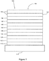
- FIG. 1 shows an organic light emitting device 100.
- Device 100 may include a substrate 110, an anode 115, a hole injection layer 120, a hole transport layer 125, an electron blocking layer 130, an emissive layer 135, a hole blocking layer 140, an electron transport layer 145, an electron injection layer 150, a protective layer 155, and a cathode 160.
- Cathode 160 is a compound cathode having a first conductive layer 162 and a second conductive layer 164.
- Device 100 may be fabricated by depositing the layers described, in order. The properties and functions of these various layers, as well as example materials, are described in more detail in US 7,279,704 at cols. 6-10.
- An example of a p-doped hole transport layer is m-MTDATA doped with F.sub.4-TCNQ at a molar ratio of 50:1, as disclosed in U.S. Patent Application Publication No. 2003/0230980 .
- Examples of emissive and host materials are disclosed in U.S. Pat. No. 6,303,238 to Thompson et al. .
- An example of an n-doped electron transport layer is BPhen doped with Li at a molar ratio of 1:1, as disclosed in U.S. Patent Application Publication No. 2003/0230980 .
- U.S. Pat. Nos. 5,703,436 and 5,707,745 . disclose examples of cathodes including compound cathodes having a thin layer of metal such as Mg:Ag with an overlying transparent, electrically-conductive, sputter-deposited ITO layer. The theory and use of blocking layers is described in more detail in U.S. Pat. No. 6,097,147 and U.S. Patent Application Publication No. 2003/0230980 .
- injection layers are provided in U.S. Patent Application Publication No. 2004/0174116 .
- a description of protective layers may be found in U.S. Patent Application Publication No. 2004/0174116 .
- FIG. 2 shows an inverted OLED 200.
- the device includes a substrate 210, a cathode 215, an emissive layer 220, a hole transport layer 225, and an anode 230.
- Device 200 may be fabricated by depositing the layers described, in order. Because the most common OLED configuration has a cathode disposed over the anode, and device 200 has cathode 215 disposed under anode 230, device 200 may be referred to as an "inverted" OLED. Materials similar to those described with respect to device 100 may be used in the corresponding layers of device 200.
- FIG. 2 provides one example of how some layers may be omitted from the structure of device 100.
- FIGS. 1 and 2 The simple layered structure illustrated in FIGS. 1 and 2 is provided by way of non-limiting example, and it is understood that embodiments of the invention may be used in connection with a wide variety of other structures.
- the specific materials and structures described are exemplary in nature, and other materials and structures may be used.
- Functional OLEDs may be achieved by combining the various layers described in different ways, or layers may be omitted entirely, based on design, performance, and cost factors. Other layers not specifically described may also be included. Materials other than those specifically described may be used. Although many of the examples provided herein describe various layers as comprising a single material, it is understood that combinations of materials, such as a mixture of host and dopant, or more generally a mixture, may be used. Also, the layers may have various sublayers.
- hole transport layer 225 transports holes and injects holes into emissive layer 220, and may be described as a hole transport layer or a hole injection layer.
- an OLED may be described as having an "organic layer" disposed between a cathode and an anode. This organic layer may comprise a single layer, or may further comprise multiple layers of different organic materials as described, for example, with respect to FIGS. 1 and 2 .
- OLEDs comprised of polymeric materials (PLEDs) such as disclosed in U.S. Pat. No. 5,247,190 to Friend et al. .
- PLEDs polymeric materials
- OLEDs having a single organic layer may be used.
- OLEDs may be stacked, for example as described in U.S. Pat. No. 5,707,745 to Forrest et al. .
- the OLED structure may deviate from the simple layered structure illustrated in FIGS. 1 and 2 .
- the substrate may include an angled reflective surface to improve outcoupling, such as a mesa structure as described in U.S. Pat. No. 6,091,195 to Forrest et al. , and/or a pit structure as described in U.S. Pat. No. 5,834,893 to Bulovic et al. .
- any of the layers of the various embodiments may be deposited by any suitable method.
- preferred methods include thermal evaporation, ink-jet, such as described in U.S. Pat. Nos. 6,013,982 and 6,087,196 , organic vapor phase deposition (OVPD), such as described in U.S. Pat. No. 6,337,102 to Forrest et al. , and deposition by organic vapor jet printing (OVJP), such as described in U.S. patent application Ser. No. 10/233,470 .
- OVPD organic vapor phase deposition
- OJP organic vapor jet printing
- Other suitable deposition methods include spin coating and other solution based processes. Solution based processes are preferably carried out in nitrogen or an inert atmosphere.
- preferred methods include thermal evaporation.
- Preferred patterning methods include deposition through a mask, cold welding such as described in U.S. Pat. Nos. 6,294,398 and some of the deposition methods such as ink-jet and OVJD. Other methods may also be used.
- the materials to be deposited may be modified to make them compatible with a particular deposition method.
- substituents such as alkyl and aryl groups, branched or unbranched, and preferably containing at least 3 carbons, may be used in small molecules to enhance their ability to undergo solution processing. Substituents having 20 carbons or more may be used, and 3-20 carbons is a preferred range. Materials with asymmetric structures may have better solution processibility than those having symmetric structures, because asymmetric materials may have a lower tendency to recrystallize. Dendrimer substituents may be used to enhance the ability of small molecules to undergo solution processing.
- Devices fabricated in accordance with embodiments of the invention may be incorporated into a wide variety of consumer products, including flat panel displays, computer monitors, televisions, billboards, lights for interior or exterior illumination and/or signaling, heads up displays, fully transparent displays, flexible displays, laser printers, telephones, cell phones, personal digital assistants (PDAs), laptop computers, digital cameras, camcorders, viewfinders, micro-displays, vehicles, a large area wall, theater or stadium screen, lighting fixtures, or a sign.
- PDAs personal digital assistants
- Various control mechanisms may be used to control devices fabricated in accordance with the present invention, including passive matrix and active matrix. Many of the devices are intended for use in a temperature range comfortable to humans, such as 18 degrees C. to 30 degrees C., and more preferably at room temperature (20-25 degrees C.).
- the materials and structures described herein may have applications in devices other than OLEDs.
- other optoelectronic devices such as organic solar cells and organic photodetectors may employ the materials and structures.
- organic devices such as organic transistors, may employ the materials and structures.
- halo, halogen, alkyl, cycloalkyl, alkenyl, alkynyl, arylkyl, heterocyclic group, aryl, aromatic group, and heteroaryl are known to the art, and are defined in US 7,279,704 at cols. 31-32.
- the term “capping layer” may refer to a layer of material that is deposited over the top electrode of an OLED (which is typically the cathode for top emission devices).
- the layer is typically used to enhance the amount of light outcoupled from the OLED.
- the layer may be made of any suitable material (such as Alq 3 ), and is preferably transparent, semi-transparent, or translucent.
- the term “total capping layer” may refer to the combination of all of the capping layers disposed over (and optically coupled to) an OLED. For instance, if a first and second capping layer are disposed over an OLED such that they are all optically coupled, the total capping layer of the OLED is the combination of the first and second capping layers.
- the “total optical thickness” is the optical thickness of the total capping layer.
- optically coupled may refer to a configuration in which substantially all of the light that is emitted from, or that propagates through, a surface of a first component also propagates through a substantially parallel surface of a second component.
- a “component” may include an organic device (e.g. OLED, transparent OLED, or top-emission OLED), a layer of an organic device (such as an organic layer, an emitting layer, etc.), a capping layer (which may be disposed over an organic device), a substrate, and/or an electrode of an organic device.
- an OLED may be optically coupled to a capping layer if substantially all of the light that is emitted from the OLED in a direction perpendicular to one of its electrodes also propagates through a surface of a capping layer that is substantially parallel to the electrode.
- the term "deposit” or “depositing” includes any known method of fabricating a layer of an organic device on a first substrate, including VTE, OVJP, OVJD, stamping, ink jet deposition, LITI, LIPS, as well as fabrication (including photolithography) of a layer on a second substrate followed by alignment of the first and second substrates. Stamping (both additive ( i.e. cold welding) and subtractive) is described in detail in U.S. Pat. No. 6,294,398 , U.S. Pat. No. 6,895,667 and U.S. Pat. No. 7,964,439 .
- a capping layer may be "common" to a plurality of organic devices if it is disposed over (e.g. covering) a substantial portion of each of the plurality of OLEDs. For instance, if a capping layer is common to a first and a second OLED, but is not common to a third OLED, then the capping layer will be disposed over a substantial portion of both the first and second OLED, but will not be substantially disposed over the third OLED.
- the term "blanket layer” may refer to a layer that is common to all of, or substantially all of, the OLEDs on a substrate.
- a blanket layer may be deposited through a mask that prevents material from depositing around the edges of the substrate (for example, in the area required for encapsulation or in areas requiring electrical contact from an external power supply or video signal).
- the deposition of a blanket layer generally docs not involve deposition of materials onto the substrate through a mask that defines features on the substrate (such as individual pixels of one particular color), such as an FMM. In most cases, the mask used does not need to be aligned to a degree of precision that exactly matches the deposition holes with sub-pixel size features on the substrate.
- a "patterned mask” or “fine metal mask” may refer to masks that may be used to deposit materials onto a substrate.
- the organic and metal layers are deposited through a "patterned mask” including blanket and/or common layers.
- the opening (i.e. "hole") in a "patterned mask” is usually large and covers a significant portion of the display or lighting panel area.
- an FMM may be used to deposit features having a pattern resolution smaller than the entire active (light emitting) area of the substrate.
- an FMM has one dimension that is of the order of the dimensions of a portion of the sub-pixels (usually of one color) that is disposed on the substrate.
- An FMM is thereby typically utilized for the deposition of the emissive layer of an organic device, where the differing colors of the display are each deposited separately through an FMM designed to only allow deposition on a portion of the active OLEDs present in the display (e.g. an FMM through which only the red emissive layer is deposited, another FMM through which only the green emissive layer is deposited, etc.).
- All masks whether "patterned" (such as those with a large opening for common deposition) or an FMM require some degree of alignment.
- the FMM requires a far tighter alignment tolerance (e.g. on the order of the dimension of a portion of the sub-pixels) and thereby usually takes longer to align, which may add significantly to the time and cost of manufacturing.
- FMMs also typically require more regular maintenance (i.e. replacement or regular cleaning) than large area "patterned" masks, as the smaller "holes" in the FMM (through which material is deposited) can reduce in size as a function of deposition/production time as material is deposited onto them. This can cause problems in the display area as the deposition area of the FMM is reduced beyond its original design.
- a build up of material on an FMM can also cause issues related to "flaking” (i.e. material falling off the mask into the chamber or getting onto the substrate), which may create yield problems. These issues may not be as significant for a "patterned" large area mask, as the surface area of the mask onto which material can be deposited is far smaller (i.e. there are larger openings for material to be deposited through).
- optical thickness may refer to the product of the physical thickness of an isotropic optical element and its refractive index.
- physical thickness of a capping layer refers to the length of the capping layer in a direction that is substantially perpendicular to the surface of the substrate that an OLED is disposed over.
- the term “optimized” or “optimal” may refer to maximizing the lifetime or efficiency of an OLED, which may result from reducing the loss of efficiency to less than approximately 5%.
- a capping layer is deposited onto the top electrode to enhance the emission from the device. That is, a capping layer (which typically includes high transparency materials) is employed to limit attenuation of the light emitted from a device. If the capping layer is chosen properly, the capping layer can enhance the output of a top-emitting device by, for instance, increasing the luminance by reducing the outcoupling losses from the device due to processes such as internal waveguiding.
- the optimal thickness (in terms of efficiency) of a capping layer made of a given material differs depending on the light emission color (and thereby the wavelength of the light).
- the inventors have recognized that one way to achieve maximum efficiency for a device comprising a plurality of OLEDs emitting light of different wavelengths is to have different capping layers for each of the organic devices.
- a side-by-side red-green-blue (RGB) display embodiments provided herein may utilize different optical thicknesses of the capping layer for each of the RGB pixels (e.g. a first capping layer optical thickness disposed over the blue pixels, a second capping layer optical thickness disposed over the green pixels, and a third capping layer optical thickness disposed over the red pixels).
- different materials may be used for the different capping layers for each of the different colored OLEDs to achieve a similar optimization (which may thereby vary the optical thickness of the capping layer based on the index of refraction of the materials).
- a similar optimization which may thereby vary the optical thickness of the capping layer based on the index of refraction of the materials.
- This use of only a single capping layer results in less than optimal performance for the OLEDs that emit light having a different wavelength than the one for which the capping layer thickness is optimized.
- this is the red and green organic devices when the capping layer is chosen to maximize the blue OLEDs.
- using a less than optimal capping layer e.g. a capping layer optimized for blue light emissions
- 'potential efficiency it is meant the efficiency of a device if the capping layer is chosen to optimize its efficiency. Therefore, the device as whole does not operate as efficiently as possible.
- Embodiments provided herein disclose devices (such as displays) that have the light emissions of each OLED optimized by utilizing a total capping layer for each organic device that has an optical thickness that is different for each color light emission ( e.g. by providing different thicknesses and/or materials as needed).
- the effects of the interference patterns created in such top-emissions devices are dictated in part by the optical thickness of the capping layer and the wavelength of the light emissions and can thereby be minimized.
- the thickness of the capping layer may effect the optical efficiency of OLEDs, there has been no recognition of this solution, which provides a novel approach for dcviccs having a plurality of OLEDs emitting multiple colors (e.g . a red, green, and blue display).
- achieving optimization of light emission for each color OLED in a device by utilizing capping layers having different optical thicknesses could substantially increase the cost of manufacturing such devices using traditional processes. That is, providing different capping layer thicknesses or materials could require the use of multiple deposition processes or steps. For instance, using traditional approaches may require the use of multiple patterned masks (e.g . FMMs in combination with VTE deposition through the FMM) for depositing each of the different materials and/or different thicknesses of the same material over each OLED color.
- a typical RGB device that is, a device comprising OLEDs having one of three different colors
- regular maintenance i.e. replacement or regular cleaning
- FMMs often increases the chances of certain defects occurring in the manufacturing process, such as issues related to the reduction of the area that is deposited through the mask (based on the increase of material deposited in the "holes" of the mask) thereby causing problems in the lighting or display area.
- a build up of material on an FMM can also cause issues due to "flaking" - i.e. material falling off the mask into the chamber or getting onto the substrate, which may induce yield problems. Therefore, the inventors have further recognized the preference of utilizing alternative deposition techniques to depositing multiple capping layers.
- Embodiments provided herein allow for the use of a different capping layer optical thickness for each pixel and/or color OLED (thereby enabling optimization of the output efficiency of each of the OLEDs of a device), without requiring the additional steps of performing deposition using a FMM.
- red, green, and blue OLEDs may be fabricated utilizing known techniques including a common capping layer (e.g. a capping layer that may be common to multiple pixels that are different colors).
- This capping layer may be designed so as to match ( i.e. optimize) the blue pixel, as typically this pixel may also require the smallest thickness of material.
- the additional capping layer material needed to optimize the red and green pixels may then be deposited so as to be optically coupled with each pixel.
- application of the additional material may not be done using a FMM and/or VTE deposition of the material.
- embodiments provided herein may deposit the additional material using, for example, laser induced thermal imaging (LITI) and/or laser induced pattern-wise sublimation (LIPS) deposition onto the common capping layer.
- LITI laser induced thermal imaging
- LIPS laser induced pattern-wise sublimation
- some examples of LITI processes utilize a donor film (donor), a highly accurate laser exposure system, and a substrate (receptor).
- the donor film may first be laminated onto the substrate using any known method such that the donor and receptor are in intimate contact.
- the donor may comprise a light-to-heat conversion (LTHC) layer that converts laser energy to heat.
- the LTHC layer comprises material that absorbs the wavelength of irradiation and converts a portion of the incident radiation into sufficient heat to enable the transfer of a thermal transfer layer (typically organic materials) from the donor to the receptor.
- the donor is then exposed (in an imagewise pattern) with a laser beam from the highly accurate laser exposure system, which is absorbed by the LTHC layer.
- LIPS processes may be similar to LITI processes with the exception that the donor and receptor may first be put together in a vacuum and fixed with a clamping mechanism. The donor, receptor, and clamping mechanism are then removed from the vacuum (and are held together by atmospheric pressure applied to either substrate), while a gap between the pixels may be maintained by the height of a pixel defined layer (PDL). A laser is then used to heat the desired portions of the donor (e.g. glass substrate having donor materials) such that the donor materials are transferred to the receptor by vacuum sublimation.
- PDL pixel defined layer
- LITI and LIPS processes have certain disadvantages that typically make them less then ideal, particularly for deposition of materials that have electro-active properties. For instance, in LITI processes, contact between the donor film and any emitting layer can degrade the device; the transferred layer interface is formed by a lamination process, which may also degrade a device; and the process may be highly sensitive to particle contamination, which may disrupt electrical contacts (although this may be reduced by the LIPS process by the creation of a vacuum between the donor and the substrate). Both deposition techniques also require the application of very high power density energy. Such application can cause thermal degradation of the materials or require additional constraints on the thermal properties of the materials being deposited ( e.g . Tg, sublimation temperature range, etc.). These constraints limit the choice of material that can be used in the electro-active components.
- capping layer materials are not electrically active components in the OLED device.
- the inventors have recognized thereby that concerns and complications typically related to the LITI process and its deleterious effect from a lifetime perspective are reduced when using this process for depositing additional capping layer thicknesses and materials.
- the LITI process could also be potentially performed in a glovebox or in air. Such a process would likely be far less costly than the FMM/VTE approach to depositing optimized capping layers for each OLED.
- neither LITI nor LIPS requires the use of a mask, making it highly adaptable as there is no need for retooling if a design is changed.
- the use of laser deposition techniques can be highly precise, and do not require the alignment of masks to deposit materials.
- the capping layer is not deposited by VTE through an FMM, then it can be done offline ( i.e. separate from an in-line manufacturing process) and thereby simplify the manufacturing process. This is due in part because the materials would not be directly deposited onto the substrate that comprises the organic materials, which are often less tolerant to manufacturing and deposition conditions (such as heat).
- the capping layer or capping layers may not be deposited directly onto the organic devices.
- the capping layer material may be deposited onto a second substrate, such as a display cover glass.
- this may be the capping layer material for optimizing only red OLEDs.
- This patterning can be done using a variety of deposition methods including photolithography, LITI, LIPS, stamping, or inkjet printing as the capping layer is not an electrically active component in the device and therefore concerns over damage during deposition are lessened.
- the red capping layer material may be deposited in such a way as to enable it to be aligned with the corresponding red sub pixel pattern on the display backplane.
- the red capping layer When the cover glass and backplane are then mated ( i.e. coupled) together the red capping layer would then be optically coupled to a common capping layer (which may in some embodiments be deposited as a blanket layer - e.g. not through an FMM) over the red sub pixels enabling the common capping layer and red capping layer to be optically coupled to the red sub pixels.
- a common capping layer which may in some embodiments be deposited as a blanket layer - e.g. not through an FMM
- the red pixel is the color that usually is most disadvantaged in terms of efficiency. Therefore, in some embodiments, for the fabrication methods described above, the most important color (after blue) may be the red pixel from an optimization perspective. Therefore it may be possible to only apply the additional capping layer material to the red sub-pixels (assuming there is already a common capping layer - i.e. that the capping layer is common to a plurality of OLEDs that is designed to optimize the blue OLEDs) in order to simplify the fabrication process, while achieving an increase in performance of the device.
- a first capping layer that is common to all of the OLEDs (i.e. the red, blue, and green OLEDs) and a second capping layer that is optically coupled to only the red OLEDs.
- a second capping layer that is optically coupled to only the red OLEDs.
- Described below are exemplary embodiments of devices, and exemplary methods of manufacturing devices, comprising organic devices and different capping layers (i.e. non-common). The embodiments are described for illustration purposes only and are not thereby intended to be limiting.
- the non-common capping layers are not deposited through an FMM but by using LITI or LIPS.
- a method for fabricating an organic device having a non-common capping layer comprises providing a plurality of OLEDs on a first substrate.
- "Providing” may comprise any known manner of obtaining a substrate having a desired number and type of organic devices disposed thereon. This includes, by way of example, depositing the OLEDs on the substrate using any known technique, including those described above.
- embodiments also comprise purchasing or otherwise obtaining a substrate that already has some or all of the OLEDs (or components thereof) disposed thereon. In cases where only some of the components are provided on a substrate, it is also envisioned that “providing” encompasses completing the components (e.g. by depositing additional layers of materials) of the OLEDs on the substrate.
- Each of the plurality of OLEDs includes a transmissive top electrode. That is, the top electrode may be transparent, semi-transparent, or translucent such that light may propagate through the top electrode.
- the OLED may be a transparent OLED or a top-emission OLED.
- Top-emitting OLEDs are often better suited for active-matrix applications because, for instance, they may be more easily integrated with a non-transparent transistor backplane. This is often the case for displays.
- the plurality of OLEDs includes a first portion of OLEDs and a second portion of OLEDs that is different from the first portion. That is, the OLEDs that comprise the first portion are separate and distinct from the OLEDs that comprise the second portion such that there is no overlap between these two designations.
- the first portion may comprise only OLEDs that emit a single color.
- the first method further includes depositing a first capping layer over at least the first portion of the plurality of OLEDs such that the first capping layer is optically coupled to at least the first portion of the plurality of OLEDs.
- the capping layer is often used in top emission organic devices to decrease the absorption and interference loses created by the transparent conductor and the reflectivity of the bottom electrode.
- the capping layer may comprise any suitable material, and may comprise a dielectric material. In some embodiments, the capping layer is preferably Alq 3 .
- the first capping layer may be deposited using any suitable method, including those described above.
- the first method also comprises depositing a second capping layer over at least the second portion of the plurality of OLEDs such that the second capping layer is optically coupled to the second portion of the plurality of OLEDs but not the first portion of the plurality of OLEDs. That is, in some embodiments, the second capping layer is deposited so that it is disposed over the second portion of the plurality of OLEDs, but not the first portion so that the optical thickness of the total capping layer over the first portion and the second portion of the plurality of OLEDs may be different.
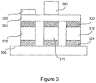
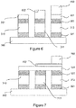
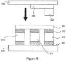
- the total capping layer may refer to the combination of each of the capping layers disposed over an OLED - for instance, if the first and second capping layer are both optically coupled to the second portion of the plurality of OLEDs, then the total capping layer is the combination of the first and second capping layer. This is illustrated in the various embodiments shown in Figs. 3 and 5-9 , which are described below.
- the second capping layer is deposited using a method that does not utilize an FMM, for the reasons noted.
- the first method and resulting device described above may provide advantages over current devices. For instance, by providing a first and a second capping layer, the device may optimize the emissions from at least two different color emitting OLEDs. For instance, current devices (such as displays comprising OLEDs) only utilize a single capping layer that is common across all of the organic devices, regardless of the wavelength of the light emission from each device. The result is that while the OLEDs that emit light having one color may be optimized, the other organic devices are not effectively out coupled so as to provide maximum efficiency. It should be noted that the effect of the optical thickness on different light emissions was described above, particularly in H.
- the second capping layer is not deposited through a patterned mask specifically not through an FMM.
- FMM additional deposition steps using FMMs may increase expense and time to manufacture organic devices.
- embodiments may provide methods that are more cost effective, flexible, and time efficient.
- these alternative deposition methods have not been utilized in applying capping layers to top emission devices (let alone non-common capping layers having different optical thicknesses).
- the inventors have recognized that such techniques, while having limitations that may make them less than ideal when depositing electrically active components, do not present some or all of those deficiencies with regard to capping layers because the capping layers are not electrically active (they may comprise dielectric materials).
- the second capping layer is deposited using at least one of: laser induced thermal imaging (LITI) or laser induced pattern-wise sublimation (LIPS). While these exemplary deposition techniques may require the application of very high power density energy and may thereby cause thermal degradation of the materials or require additional constraints on the thermal properties (as described above) making them not preferable for depositing electro-active components, these same deficiencies are reduced when applying non-electro-active layers. However, in some embodiments, any deposition technique that does not involve the use of an FMM or similar technique may be used.
- the first method as described above further includes depositing the first capping layer over at least the second portion of the plurality of OLEDs such that the first capping layer is optically coupled to the second portion of the plurality of OLEDs. This is illustrated in the exemplary embodiments shown in Figs. 3 and 7-9 .
- the first capping layer is optically coupled to OLEDs that emit light in different colors, whereas the second capping layer is optically coupled to OLEDs that emit light of a single color.
- the first capping layer is optically coupled to at least one color of OLEDs that the second capping layer is not optically coupled to.
- the first capping layer may be optically coupled to a plurality of blue, green, and red OLEDs, whereas the second capping layer is optically coupled to only a plurality of red OLEDs.
- the first capping layer may comprise a blanket layer. That is, the first capping layer may be deposited so as to be disposed over all, or substantially all, of the OLEDs on a substrate of a device such that it is common to each of the OLEDs. This may have the advantage that the first capping layer need not be deposited through a FMM or other expensive and/or complex deposition process.
- the optical thickness of the first capping layer may be selected so as to optimize the OLEDs that emit light of a particular color. In some embodiments, the optical thickness of the first capping layer may be selected so as to correspond to the smallest thickness that optimizes at least one of the OLED emission colors.
- additional capping layers may be disposed over the first capping layer so that the total capping layer that is optically coupled to OLEDs having a different color are also optimized (i.e. the optical thickness is optimized for light emissions having a particular wavelength).
- the first capping layer is not deposited over the second portion of the plurality of OLEDs such that the first capping layer is not optically coupled to the second portion of the plurality of OLEDs. This is shown in Fig. 4 , whereby none of the optical layers are common across OLEDs of different colors.
- the plurality of OLEDs are transparent OLEDs and/or are top emission OLEDs. Again, top emission OLEDs may be better suited for certain implementations, such as displays.
- the first capping layer has a first total optical path that is constant over the first portion of the plurality of OLEDs
- the second capping layer may comprise a second total optical path that is constant over the second portion of the plurality of OLEDs
- the first total optical path and the second total optical path are different. This may be the case in some embodiments when the plurality of OLEDs comprise OLEDs that emit light of different wavelength, and thereby the optical thickness that maximizes the efficiencies of the OLEDs is also different. Thus, embodiments that provide two different optical thickness may be capable of maximizing two different color OLEDs.
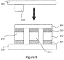
- the step of depositing the second capping layer may comprise depositing the second capping layer onto portions of a second substrate and aligning the second capping layer over at least the second portion of the plurality of OLEDs. This is illustrated in Figs. 8-9 , and will be described in more detail below.
- the second capping layer is deposited using LITI or LIPS. Depositing the second capping layer on a second substrate may be less expensive and complex compared to deposition of the capping layers directly over the OLEDs (e.g.
- the deposition on the second substrate may be done without the risk of damaging the organic materials (which may be relatively sensitive to damage from other deposition and manufacturing processes). Moreover, if a manufacturing error was to occur in this deposition process, it would not be as costly as there are no other OLED materials disposed on the second substrate.
- the step of aligning the second capping layer over at least the second portion of the plurality of OLEDs comprises depositing the second capping layer onto portions of the second substrate such that the second capping layer is over at least the second portion of the plurality of OLEDs when the second substrate is coupled to the first substrate. That is, for example, the second capping layer may be optically coupled to the second portion of the plurality of OLEDs when the first and second substrates are coupled.
- a device such as a display
- the first capping layer is optically coupled to the second capping layer when the first substrate is coupled to the second substrate. This may be the case, for instance, when the first capping layer is common to a plurality of OLEDs that emit light in different colors.
- the second substrate is a display cover.
- the coupling of the first and the second substrates can serve to encapsulate the organic devices.
- materials in an OLED arc sensitive to air and moisture, which can lead to degradation of the organic materials and/or quenching of excited states within the molecules if they are exposed to such atmospheric conditions. Utilizing the second substrate (which may comprise glass) in this manner can thereby serve multiple purposes.
- depositing the first capping layer may comprise either one of, or some combination of: FMM and VTE. This may be the case when the first capping layer is not common to all, or substantially all, of the OLED devices on the first substrate.
- none of the capping layers are deposited by either one of, or some combination of: FMM and VTE.
- all of the capping layers may be deposited using LITI or LISP processes, which provide the advantages described above over traditional deposition processes. In this manner, embodiments may provide the advantage of not using an FMM, which can add to the complexity of manufacturing OLEDs, and also introduces various sources of error such as mask deformation.
- the plurality of OLEDs may include a plurality of red OLEDs, a plurality of green OLEDs, and a plurality of blue OLEDs. This is typically the case for most displays (and light panels), as most colors can be replicated by using the combination of red, green, and blue light, including white light.
- the first and second portions of the plurality of OLEDs may each comprise OLEDs of particular colors, and in examples which are not covered by the claims, there may not be any overlap.
- the first portion of the plurality of OLEDs may comprise a plurality of blue OLEDs and/or the second portion of the plurality of OLEDs may comprise only a plurality of the green OLEDs and a plurality of the red OLEDs. It follows thereby that in some examples the first capping layer (which is optically coupled to the first portion of the plurality of OLEDs - i.e. the blue OLEDs) may be different than the second capping layer (which is optically coupled to the second portion of the plurality of OLEDs - i.e. the green and red OLEDs).
- the first capping layer optimized for the light emissions in the blue spectrum (because the first capping layer may be optimized for only the blue OLEDs), while simultaneously optimizing the second capping layer for either the red or green OLEDs (or the second capping layer may have an optical thickness that is a compromise between the optimal optical thickness for each device).
- the second portion of the plurality of OLEDs comprises only a plurality of the red OLEDs or a plurality of the green OLEDs. The second capping layer may thereby be optimized for either of the light emissions of the green or red OLEDs.
- the plurality of OLEDs may also include a third portion of OLEDs that is different from the first and second portions.
- the method may further include the step of depositing a third capping layer over at least the third portion of the plurality of OLEDs such that the third capping layer is optically coupled to at least the third portion of the plurality of OLEDs.
- a third capping layer may allow for the optimization of the emissions for OLEDs having three different color emissions (e.g. red, blue, and green). Although it is possible to obtain three different optical thicknesses using only two depositions of capping layers, it may be more practical to utilize three deposition processes (as it may be difficult to provide three different thicknesses that each optimize the light emission from a different OLED color). Exemplary embodiments of such configurations are shown in Figs. 3-7 and 9 , and will be described in more detail below. In some embodiments, the third capping layer is not optically coupled to the first portion and the second portion of the plurality of OLEDs.
- the third capping layer may not be common to all, or substantially all of the OLEDs of the device ( i.e. it may not be a blanket layer). Moreover, by providing capping layers that are not common to all of the other OLEDs, embodiments may provide non-common capping layers that may be optimized for a particular subset of the OLEDs of a device (e.g. based on the color of the emission). In some embodiments, the third capping layer is not optically coupled to the first portion or the second portion of the plurality of OLEDs.
- the third capping layer is not deposited through a patterned mask and, preferably, through an FMM. Again, as described above, deposition through a FMM or other traditional deposition processes can be, for instance, cost prohibitive when providing multiple non-common capping layers.
- the inventors have recognized the benefits of depositing the third capping layer using these alternative techniques, such as using at least one of: laser induced thermal imaging (LITI) or laser induced pattern-wise sublimation (LIPS).
- LITI laser induced thermal imaging
- LIPS laser induced pattern-wise sublimation
- embodiments and features described herein may be combined and utilized with methods of fabricating devices, and the devices themselves, that comprise non-common capping layers that are deposited using such alternative deposition techniques ( i.e. not through the use of an FMM).
- the plurality of OLEDs include a plurality of red OLEDs, a plurality of green OLEDs, and a plurality of blue OLEDs
- the plurality of OLEDs also include a third portion of OLEDs that is different from the first and second portions
- the first method further includes the step of depositing a third capping layer over at least the third portion of the plurality of OLEDs such that the third capping layer is optically coupled to at least the third portion of the plurality of OLEDs
- the step of depositing the third capping layer may comprise depositing the third capping layer onto portions of a second substrate and aligning the third capping layer over the third portion of the plurality of OLEDs.
- the third capping layer may be deposited onto the second substrate using, for example, at least one of: photolithography, LITI, LIPS, stamping, or inkjet printing.
- the capping layer or layers are deposited on a second substrate allow for more options in the deposition process, typically a reduction in cost, and usually more error tolerance because the substrate does not comprise organic material, which may often be sensitive to such processes.
- the third capping layer may be aligned with the third portion of OLEDs by depositing the third capping layer onto portions of the second substrate such that the third capping layer is optically coupled to the third portion of the plurality of OLEDs when the second substrate is coupled to the first substrate.
- the third capping layer may also be optically coupled to the first capping layer when the first substrate is coupled to the second substrate. This may be the case in embodiments where the first capping layer is a blanket layer, or is common to both the first and third portions of the plurality of OLEDs. A non-limiting example of such an embodiment is shown in Fig. 9 .
- the second substrate is a display cover ad may serve to encapsulate the organic devices when it is coupled to the substrate that has the OLEDs disposed thereon.
- the plurality of OLEDs include a plurality of red OLEDs, a plurality of green OLEDs, and a plurality of blue OLEDs, where the plurality of OLEDs also includes a third portion of OLEDs that is different from the first and second portions, and where the method includes the step of depositing a third capping layer over at least the third portion of the plurality of OLEDs such that the third capping layer is optically coupled to at least the third portion of the plurality of OLEDs, the first, second, and third portions of the plurality of OLEDs may each comprise OLEDs of various different colors.
- the third portion of the plurality of OLEDs may comprise only a plurality of the red OLEDs
- the second portion of the plurality of OLEDs may comprise only a plurality of the green OLEDs
- the first portion of the plurality of OLEDs may comprise only a plurality of the blue OLEDs. In this manner, it may be possible to optimize the total capping layer over each of the plurality of OLEDs ( i.e. for each color).
- the total capping layer over each OLED in the first portion of the plurality of OLEDs may be the same (and may optimize the blue emissions), the total capping layer over each OLED of the second portion may be the same (and may optimize the red emissions), and the total capping layer over each OLED of the third portion may be the same (and may optimize the green emissions).
- any color OLED comprise each of the first, second, and third portions of the plurality of OLEDs as described above.
- the third portion of the plurality of OLEDs may comprise only a plurality of the green OLEDs
- the second portion of the plurality of OLEDs may comprise only a plurality of the red OLEDs
- the first portion of the plurality of OLEDs may comprise only a plurality of the blue OLEDs. It follows thereby that examples, which are not covered by the claims may also comprise any combination of the first, second, and third capping layers such that the total capping layer over each of the first, second, and third portion of OLEDs is optimized.
- the first capping layer may have a thickness that is optimized for at least one of the plurality of red OLEDs, green OLEDs, and blue OLEDs. That is, the first capping layer as described above may be designed to have an optical thickness to optimize the emissions of any of the OLEDs in the device, without the need for any additional capping layers.
- the first capping layer has a thickness that is optimized for the plurality of blue OLEDs. This is due in part to the fact that the blue emission is typically optimized by utilizing the least thick (i.e. thinnest) capping layer. It is preferred that the first capping layer have a thickness that optimizes the light emission for the shortest wavelength OLED because the first capping layer may then be a blanket layer such that it is common to all, or substantially all, of the OLEDs of the device. The second and third capping layers may then be disposed over the first capping layer and optically coupled to OLEDs that emit light having a higher wavelength because the optical thickness of the capping layer for these devices is usually greater.
- the first capping layer can be used in conjunction with the second and third capping layers for a total capping layer over the second and third portions of the plurality of OLEDs.
- the first capping layer has an optical thickness that is less than approximately 125 nm. In some embodiments, the first capping layer is within the range of 90 to 130 nm. This range typically includes the optical thickness to optimize the blue OLEDs.
- the optical thickness of the capping layer (or layers) that is optically coupled to the OLED be set to approximately the quarter wavelength of the OLED light emission. This may thereby reduce interference patterns and establish a maximum as to the amount of light emissions.
- the capping layers may comprise many different characteristics.
- the first capping layer may comprise any suitable materials, such as those that are frequently used and known in the art, which may include Alq 3 .
- the first capping layer is substantially transparent for light having a wavelength approximately equal to a wavelength of light that is emitted by each OLED that the first capping layer is optically coupled to. It is preferred that the capping layer is transparent so as to reduce emission loses of the organic devices.
- the first capping layer has an index of refraction that is approximately in the range of 1 and 2.5. Typically, the higher the index of refraction, the less physical thickness is needed for the capping layers (because the optical thickness is the product of the physical thickness and the index of refraction).
- the increase in index of refraction may also decrease the critical angle at the boundary of the capping layer and may introduce additional types of losses.
- the first capping layer has an index of refraction that is approximately within the range of 1.5 and 2.
- the first capping layer has an optical thickness that results in a loss of efficiency for the plurality of green OLEDs that is within the range of approximately 5 to 10%. This loss may be due to the first capping layer having an optical thickness that is optimized for the blue emission OLEDs.
- the first capping layer may have an optical thickness that results in a loss of efficiency for the plurality of red OLEDs that is within the range of approximately 25 to 35% - which again may be typical when the first capping layer is optimized for the blue OLEDs.
- the second capping layer may have a thickness that is optimized for the plurality of red OLEDs and/or the plurality of green OLEDs.
- the second capping layer When the second capping layer is optimized for the plurality of green OLEDs, it may have an optical thickness that is approximately within the range of 125 to 160 nm, which is a range of values for which the capping layer is optimized for green emission OLEDs. It should be noted that in some embodiments, such as when another capping layer (such as the first capping layer, as in the invention) is common to the second portion of OLEDs, that this range may correspond to the optical thickness of the total capping layer that is in optical communication with the second portion of the plurality of OLEDs.
- the second capping layer may have an optical thickness that is less than that needed to optimize the green OLEDs alone, but when the first and the second capping layers are combined, the total optical thickness may optimize the light emissions. This is illustrated in Figs. 3 , 5-9 . Similar to the first capping layer, the second capping layer may comprise any suitable material, such as Alq 3 . The second capping layer may also be substantially transparent for light having a wavelength approximately equal to a wavelength of light that is emitted by each OLED that the second capping layer is optically coupled to.
- the second capping layer may have an index of refraction that is approximately in the range of 1 and 2.5 and preferably is approximately within the range of 1.5 and 2. This was described above with reference to the first capping layer.
- the third capping layer may have an optical thickness that is optimized for any of the OLED colors. For instance, the optical thickness may be optimized for the plurality of red OLEDs and/or the plurality of green OLEDs. This may be the case in embodiments whereby the first or the second capping layer was optimized for the blue OLEDs.
- the third capping layer when the third capping layer has an optical thickness that is optimized for the red OLEDs, the third capping layer has a thickness that is approximately within the range of 160 to 200 nm.
- the third capping layer when the first layer is common to the third portion of the plurality of OLEDs, or in examples, which are not covered by the claims and in which the second capping layer is common to the third portion of the plurality of OLEDs, then the third capping layer may have an optical thickness such that the total optical thickness of the total capping layer that is optically coupled to the third portion of the plurality of OLEDs is optimized.
- the third capping layer may comprise any suitable material, such as Alq 3 .
- the third capping layer may be substantially transparent for light having a wavelength approximately equal to a wavelength of light that is emitted by each OLED that the third capping layer is optically coupled to. Moreover, in some embodiments, the third capping layer may have an index of refraction that is approximately in the range of 1 and 2.5 and preferably approximately within the range of 1.5 and 2.
- the first, second, and third capping layers may each be designed so as to optimize one of the emission colors simultaneously.
- the first capping layer has a thickness that is optimized for the plurality of blue OLEDs
- the second capping layer has a thickness that is optimized for the plurality of green OLEDs
- the third capping layer has a thickness that is optimized for the plurality of red OLEDs.
- the device as a whole may then operate at a higher efficiency because the emissions from each color OLED is also optimized.
- each capping layer by itself does not have to provide the entire optical thickness for optimizing an OLED, but may be designed to combine with other capping layers that are also optically coupled to an OLED.
- the first capping layer has an optical thickness that is approximately within the range of 90 to 130 nm
- the second capping layer has an optical thickness that is approximately within the range of 125 to 160 nm
- the third capping layer has an optical thickness that is approximately within the range of 160 to 200 nm. This may correspond to the optimal thicknesses for optimizing blue, green, and red OLEDs respectively.
- a first apparatus comprises a plurality of OLEDs, each OLED having a first electrode, a second electrode disposed over the first electrode; and an organic electroluminescent (EL) material disposed between the first and the second electrodes.
- the OLEDs may be disposed over a common substrate such that there light emissions may combined (as in a display).
- the first apparatus further includes a first capping layer that is disposed over the second electrode of at least a first portion of the plurality of OLEDs such that the first capping layer is optically coupled to at least the first portion of the plurality of OLEDs. In this manner, the first capping layer may increase the efficiency of the emissions of at least the first portion of the plurality of OLEDs, as was described above.
- the first apparatus also comprises a second capping layer.
- the second capping layer is disposed over the second electrode of only a second portion of the plurality of OLEDs such that the second capping layer is optically coupled to the second portion of the plurality of OLEDs but not the first portion of the plurality of OLEDs.
- the optical thickness of the total capping layer that is optically coupled to the second portion of the plurality of OLEDs may be different than that which is optically coupled to the first plurality of OLEDs. This may, in some embodiments, provide the ability to optimize more than a single color OLED in such devices.
- the second capping layer in the first apparatus described above is not deposited through a FMM. Additionally, it may not be deposited by VTE. That is, as was described in detail above, the capping layers are deposited using an alternative deposition technique that has not heretofore been utilized for disposing the capping layers on a device. These techniques are LITI and LIPS, which are preferred because the capping layers are not electrically active.
- the plurality of OLEDs comprise a plurality of red OLEDs, a plurality of blue OLEDs, and a plurality of green OLEDs, such as when the device comprises a display or a light fixture.
- the second capping layer of the first apparatus is not disposed over the plurality of green OLEDs and blue OLEDs.
- the OLEDs may be optically coupled to a total capping layer that has a different optical thickness than the other OLEDs. This may then allow for the optimization of the emission of at least two of the OLED colors.
- the second capping layer is not disposed over the plurality of blue OLEDs.
- the first capping layer has an optical thickness that is optimized for the blue OLEDs such that an additional capping layer optically coupled to the blue OLEDs may not be necessary to achieve optimization.
- the apparatus further comprises a third capping layer disposed over the second electrode of at least the third portion of the plurality of OLEDs such that the third capping layer is optically coupled to at least the third portion of the plurality of OLEDs.
- a third capping layer may make it more readily achievable to optimize three separate OLED emission colors.
- the third capping layer is not optically coupled to the first or the second portions of the plurality of OLEDs.
- An example of this embodiment is show in Fig. 4 , described below. This may permit each capping layer to be designed so as to optimize the emissions of one portion of the plurality of OLEDs, without the need to combine the optical effect of the other capping layers.
- the third capping layer was not deposited through a FMM or VTE, which provides the same benefits as was described above.
- the second capping layer is not optically coupled to the plurality of blue OLEDs and the plurality of green OLEDs.
- the third capping layer is not optically coupled to the plurality of red OLEDs or the plurality of blue OLEDs. An example is shown Fig. 4 , which will be described in detail below.
- Each of the devices shown in Figs. 3-9 comprise a plurality of OLEDs (310, 311, and 312) that emit different colors (e.g. red, green and blue respectively), each having a first electrode 321 and a second electrode 322, where the second electrode 322 are the top electrodes.
- Each of the OLE'Ds are disposed on a first substrate 300.
- the first substrate may, for instance, comprise a backplane and/or TFT substrate. The remaining characteristics will be described in detail with respect to each figure.
- Fig. 3 shows a side view of an exemplary embodiment comprising a first capping layer 301, a second capping layer 302, and a third capping layer 303.
- the first capping layer 301 is disposed over the top electrode 322 of each of the OLEDs 310, 311, and 312 so as to be optically coupled to each organic device. Therefore, the first capping layer is common to OLEDs 310, 311, and 312. This may have the advantage of allowing the first capping layer 301 to be deposited as a blanket layer, and thus not require deposition through a FMM or other process.
- the first capping layer may have an optical thickness that is optimized for the OLED 312 (e.g. the blue OLED).
- a second capping layer 302 that is optically coupled to both the first capping layer 301 and OLED 310; as well as a third capping layer 303 that is optically coupled to the first capping layer 301 and the OLED 311.
- the total capping layer of the first capping layer 301 and second capping layer 302 may have a total optical thickness that optimizes OLED 310.
- the total capping layer of the first capping layer 301 and third capping layer 303 may have a total optical thickness that optimizes OLED 311.
- the exemplary embodiment may comprise a single common capping layer 301 that optimizes one OLED 312 and a second 302 and third 303 capping layer so as to maximize the other OLEDs that may emit light of a different color. In this manner, the device in Fig. 3 may be optimized.
- Fig. 4 shows a side view of an example, which is not covered by the claims, comprising a first capping layer 401, a second capping layer 402, and a third capping layer 403.
- the first capping layer 401 is not common to the plurality OLEDs 310, 311, and 312. Indeed, none of the capping layers are shown as optically coupled to any of the other capping layers, and none of the capping layers is common to a plurality of different color OLEDs.
- each of the capping layers 401, 402, and 403 may have an optical thickness that optimizes each of the OLEDs 310, 311, and 312 respectively.
- Fig. 5 shows a side view of an exemplary embodiment comprising a first capping layer 501, a second capping layer 502, and a third capping layer 503.
- capping layer 501 is common to all three OLEDs and capping layer 502 is common to OLEDs 311 and 312.
- Capping layer 503 is optically coupled to only OLED 312.
- Each capping layer 501, 502, and 503 is shown has comprising the same optical thickness.
- the total optical thickness of the total capping layer for each OLED in Fig. 5 is different based on the difference in the number of depositions of the capping layers over each device.
- Fig. 6 shows a side view of an exemplary device, not formed by the method of the present invention, comprising a first capping layer 601 and second capping layer 602.
- capping layer 601 is common to both OLED 310 and 312; and capping layer 602 is common to OLEDs 311 and 312.
- This embodiment illustrates that it is possible to have a device that comprises three different total capping layers while utilizing only two capping layers. That is, OLED 310 has a total capping layer comprising capping layer 601; OLED 311 has a total capping layer comprising capping layer 602; and OLED 312 has a total capping layer comprising capping layers 601 and 602.
- These embodiments have the advantage of only utilizing two deposition processes for depositing the capping layers, which may reduce time and costs of manufacturing.
- Fig. 7 shows a side view of an exemplary device, which can be manufactured using the method of the present invention comprising a first capping layer 701, a second capping layer 702, and a third capping layer 703.
- Fig. 7 is almost identical to Fig. 5 in that capping layer 701 is common to all three OLEDs, capping layer 702 is common to OLEDs 311 and 312, and capping layer 503 is optically coupled to only OLED 312.
- Fig. 7 shows an embodiment whereby the capping layers comprise different physical thicknesses.
- this embodiment may have the advantage of providing increased adaptability so as to more readily optimize the emissions of each of the OLEDs.
- FIGs 8 and 9 depict exemplary embodiments whereby the capping layers are deposited on a second substrate 830, such as a display panel, which is then coupled to the first substrate 300.
- a second substrate 830 such as a display panel
- the capping layer 802 is positioned such that when the substrates 300 and 830 are coupled, it is aligned with OLED 310.
- OLED 310 will be optically coupled to the common capping layer 801 and capping layer 802.
- Both OLEDs 311 and 312 are only optically coupled to capping layer 801. As was described above, this may be the case for embodiments whereby capping layer 801 is optimized for blue OLEDs.
- the red OLED (e.g. OLED 310 in Fig. 8 ) has the greatest loss of efficiency.
- providing capping layer 802 may offset or optimize OLED 310. It should be understood that some or all of the capping layers may be deposited on the second substrate 830, and in any combination, such as those discussed with reference to Figs. 3-7 .
- Figure 9 is similar to Fig. 8 in that the capping layers 902 and 903 are disposed on the second substrate 830, which may then be aligned and coupled to the first substrate 300. As shown, when the first 300 and second 830 substrate are coupled, capping layer 901 is common to all three OLEDs, capping layer 902 is common to OLEDs 311 and 312, and capping layer 903 is optically coupled to only OLED 312. Thus, the result is similar to the net effect provided by the capping layers in Figs. 5 and 7 .
- capping layers having the same or different optical properties may be provided so as to obtain different total optical thicknesses optically coupled to each of a plurality of different color OLED devices.
- the general principles remain the same as disclosed herein and are thereby contemplated as being within embodiments.
- the inventors have also performed simulations on an exemplary device comprising different capping layers for each of the different color OLEDs.
- the exemplary device had the following characteristics: The display size was 4-inches (diagonal length) and all parameters were calculated for a total display brightness of 300cd/m 2 for a white point with 40% of the pixels turned on.
- the thin film transistors (TFT) had a voltage of 5.5V and the OLEDs each had a voltage of 4V.
- the lighting panel also had a circular polarizer applied which attenuated the total panel transmission to 44%.
- the 1931 CIE coordinates for each of the OLED colors is as follows: red (0.67, 0.32) green (0.21, 0.71)and blue (0.13, 0.058).
- the combined white emission of the device had a CIE coordinate of (0.29, 0.30).
- Table 1 below shows the results of the simulations for power consumption for the exemplary 4-inch display described above, where the display has (1) the red, green, and blue pixels optimized separately with different capping layer optical thicknesses and (2) where the capping layer is optimized for the blue pixels only, but is common to red, green and blue pixels:
- the capping layer optically coupled to the red OLED comprised 100nm of Alq 3 and had an optical thickness of 170nm.
- the capping layer optically coupled to the green OLED comprised 80nm of Alq 3 and had an optical thickness of 138nm.
- the capping layer optically coupled to the blue OLED comprised 70nm of Alq 3 and had an optical thickness of 125nm.
- Table 1 Simulation Results of Exemplary Device Red Light Emission luminous efficacy [cd/A] Green Light Emission luminous efficacy [cd/A] Blue Light Emission luminous efficacy [cd/A] Power Consumption of Display [W] (1) RGB optimized capping layer 46 116 7.8 0.300 (2) B only optimized capping layer 32 104 7.8 0.343
- the light emission for this exemplary embodiment substantially increases for the red OLEDs (approximately 43.75% increase in luminance) and the green OLEDs (approximately 11.54% increase in luminance) when the capping layer that is optically coupled to each is optimized.
- the power consumption of the display decreased by 0.043 W (approximately 14.33%) as compared to the device having only a single optimized capping layer.
- the simulation confirms that devices that comprise capping layers that are optimized for each of the OLED colors have higher emission levels and thereby lower power consumption.
- the reduced power consumption and resulting increase in efficiencies may also lead to longer lifetimes of the devices. For example, using a typical red phosphorescent OLED acceleration factor of two, the lifetime of the red pixel in case 1 ( i.e. when the red OLED is optimized) can be expected to be 2.1 times longer than the device in case 2 ( i.e. not optimized) for the same initial luminance.
Landscapes
- Physics & Mathematics (AREA)
- Optics & Photonics (AREA)
- Chemical & Material Sciences (AREA)
- Inorganic Chemistry (AREA)
- Engineering & Computer Science (AREA)
- Manufacturing & Machinery (AREA)
- Electroluminescent Light Sources (AREA)
- Devices For Indicating Variable Information By Combining Individual Elements (AREA)
Claims (12)
- Verfahren, umfassend:Bereitstellen einer Vielzahl von organischen lichtemittierenden Bauelementen (OLEDs, 310, 311, 312) auf einem ersten Substrat (300), wobei jede OLED eine durchlässige obere Elektrode (322) aufweist und wobei die Vielzahl von OLEDs einen ersten Teil von OLEDs (311, 311) umfasst, und einen zweiten Teil von OLEDs (310), der sich von dem ersten Teil (311, 312) unterscheidet, wobei die Vielzahl von OLEDs eine Vielzahl von roten OLEDs (310), eine Vielzahl von grünen OLEDs (311) und eine Vielzahl von blauen OLEDs (312) umfasst;
Abscheiden einer ersten Abdeckschicht (301, 801) über zumindest dem ersten Teil der Vielzahl von OLEDs (311, 312), so dass die erste Abdeckschicht mit zumindest dem ersten Teil der Vielzahl von OLEDs (311, 312) optisch gekoppelt ist; undAbscheiden der ersten Abdeckschicht (301, 801) über wenigstens dem zweiten Teil der Vielzahl von OLEDs (310), so dass die erste Abdeckschicht (301, 801) mit dem zweiten Teil der Vielzahl von OLEDs (310) optisch gekoppelt ist; undAbscheiden einer zweiten Abdeckschicht (302, 802) nur über dem zweiten Teil der Vielzahl von OLEDs (310), so dass die zweite Abdeckschicht (302, 802) mit dem zweiten Teil der Vielzahl von OLEDs (310), aber nicht mit dem ersten Teil der Vielzahl von OLEDs (311, 312) optisch gekoppelt ist;wobei der erste Teil der OLEDs (311, 312) die Vielzahl der blauen OLEDs (312) umfasst und wobei der zweite Teil der OLEDs die Vielzahl der roten OLEDs (310) ist;wobei das Verfahren dadurch gekennzeichnet ist, dass die zweite Abdeckschicht (302, 802) nicht durch eine feine Metallmaske (FMM) abgeschieden wird;und das Abscheiden der zweiten Abdeckschicht (302, 802) zumindest eines der folgenden Verfahren umfasst: laserinduzierte Wärmeabbildung (LITI) oder laserinduzierte musterweise Sublimation (LIPS). - Verfahren nach Anspruch 1,
wobei die erste Abdeckschicht einen ersten Gesamtlichtpfad aufweist, der über den ersten Teil der Vielzahl von OLEDs konstant ist;
wobei die zweite Abdeckschicht einen zweiten Gesamtlichtpfad aufweist, der über den zweiten Teil der Vielzahl von OLEDs konstant ist; und
wobei der erste Gesamtlichtpfad und der zweite Gesamtlichtpfad unterschiedlich sind. - Verfahren nach Anspruch 1, wobei das Abscheiden der zweiten Abdeckschicht das Abscheiden der zweiten Abdeckschicht auf Teile eines zweiten Substrats und das Ausrichten der zweiten Abdeckschicht über zumindest dem zweiten Teil der Vielzahl von OLEDs umfasst.
- Verfahren nach Anspruch 1,
wobei die Vielzahl der OLEDs weiterhin einen dritten Teil von OLEDs umfasst, der sich von dem ersten und zweiten Teil unterscheidet, und
wobei das Verfahren ferner den Schritt des Abscheidens einer dritten Abdeckschicht über zumindest dem dritten Teil der Vielzahl von OLEDs umfasst, so dass die dritte Abdeckschicht mit zumindest dem dritten Teil der Vielzahl von OLEDs optisch gekoppelt ist. - Verfahren nach Anspruch 4, wobei die dritte Abdeckschicht nicht mit dem ersten Teil und dem zweiten Teil der Vielzahl von OLEDs optisch gekoppelt ist.
- Verfahren nach Anspruch 4, wobei die dritte Abdeckschicht nicht mit dem ersten Teil oder dem zweiten Teil der Vielzahl von OLEDs optisch gekoppelt ist.
- Verfahren nach Anspruch 4, bei dem die dritte Deckschicht nicht durch eine feine Metallmaske abgeschieden wird.
- Verfahren nach Anspruch 4, bei dem die Abscheidung der dritten Deckschicht zumindest eines der folgenden Verfahren umfasst: laserinduzierte thermische Bildgebung (LITI) oder laserinduzierte musterweise Sublimation (LIPS).
- Verfahren nach Anspruch 4, wobei das Abscheiden der dritten Abdeckschicht das Abscheiden der dritten Abdeckschicht auf Teile eines zweiten Substrats und das Ausrichten der dritten Abdeckschicht über dem dritten Teil der Vielzahl von OLEDs umfasst.
- Verfahren nach Anspruch 4, wobei die erste Abdeckschicht eine Dicke aufweist, die für die Vielzahl von blauen OLEDs optimiert ist.
- Verfahren nach Anspruch 10, wobei die zweite Abdeckschicht eine Dicke aufweist, die für die Vielzahl von roten OLEDs und/oder für die Vielzahl von grünen OLEDs optimiert ist.
- Verfahren nach Anspruch 11, wobei die dritte Abdeckschicht eine Dicke aufweist, die für die Vielzahl von roten OLEDs und/oder für die Vielzahl von grünen OLEDs optimiert ist.
Priority Applications (1)
| Application Number | Priority Date | Filing Date | Title |
|---|---|---|---|
| EP20155883.0A EP3671882A1 (de) | 2011-06-17 | 2012-06-15 | Nicht-gemeinsame deckschicht auf einer organischen vorrichtung |
Applications Claiming Priority (1)
| Application Number | Priority Date | Filing Date | Title |
|---|---|---|---|
| US13/163,132 US8884316B2 (en) | 2011-06-17 | 2011-06-17 | Non-common capping layer on an organic device |
Related Child Applications (2)
| Application Number | Title | Priority Date | Filing Date |
|---|---|---|---|
| EP20155883.0A Division-Into EP3671882A1 (de) | 2011-06-17 | 2012-06-15 | Nicht-gemeinsame deckschicht auf einer organischen vorrichtung |
| EP20155883.0A Division EP3671882A1 (de) | 2011-06-17 | 2012-06-15 | Nicht-gemeinsame deckschicht auf einer organischen vorrichtung |
Publications (2)
| Publication Number | Publication Date |
|---|---|
| EP2535960A1 EP2535960A1 (de) | 2012-12-19 |
| EP2535960B1 true EP2535960B1 (de) | 2020-03-25 |
Family
ID=46651338
Family Applications (2)
| Application Number | Title | Priority Date | Filing Date |
|---|---|---|---|
| EP20155883.0A Pending EP3671882A1 (de) | 2011-06-17 | 2012-06-15 | Nicht-gemeinsame deckschicht auf einer organischen vorrichtung |
| EP12172237.5A Active EP2535960B1 (de) | 2011-06-17 | 2012-06-15 | Verfahren zum Herstellen einer nicht-gemeinsamen Deckschicht auf einer organischen Vorrichtung |
Family Applications Before (1)
| Application Number | Title | Priority Date | Filing Date |
|---|---|---|---|
| EP20155883.0A Pending EP3671882A1 (de) | 2011-06-17 | 2012-06-15 | Nicht-gemeinsame deckschicht auf einer organischen vorrichtung |
Country Status (5)
| Country | Link |
|---|---|
| US (4) | US8884316B2 (de) |
| EP (2) | EP3671882A1 (de) |
| JP (2) | JP6022225B2 (de) |
| KR (4) | KR101942571B1 (de) |
| CN (2) | CN103000824B (de) |
Families Citing this family (51)
| Publication number | Priority date | Publication date | Assignee | Title |
|---|---|---|---|---|
| US8940568B2 (en) | 2012-08-31 | 2015-01-27 | Universal Display Corporation | Patterning method for OLEDs |
| US9412947B2 (en) | 2012-09-14 | 2016-08-09 | Universal Display Corporation | OLED fabrication using laser transfer |
| KR102131965B1 (ko) * | 2013-11-19 | 2020-07-09 | 삼성디스플레이 주식회사 | 유기발광 디스플레이 장치 |
| KR102125881B1 (ko) * | 2014-04-29 | 2020-06-24 | 엘지디스플레이 주식회사 | 유기 발광 소자 |
| KR20150125889A (ko) | 2014-04-30 | 2015-11-10 | 삼성디스플레이 주식회사 | 유기발광 디스플레이 장치 및 그 제조방법 |
| US10356677B2 (en) * | 2014-05-19 | 2019-07-16 | Nokia Solutions And Networks Oy | Re-establishment procedure in dual connectivity networks |
| KR102304718B1 (ko) * | 2014-07-10 | 2021-09-27 | 삼성디스플레이 주식회사 | 유기 발광 소자 |
| KR102355605B1 (ko) * | 2014-11-20 | 2022-01-26 | 엘지디스플레이 주식회사 | 유기발광다이오드 표시장치 및 그 제조방법 |
| KR102424966B1 (ko) * | 2015-02-13 | 2022-07-26 | 삼성디스플레이 주식회사 | 유기발광 표시장치 |
| CN105098094B (zh) * | 2015-07-20 | 2017-11-17 | 上海和辉光电有限公司 | 显示面板及其oled元件 |
| KR102500272B1 (ko) | 2015-09-16 | 2023-02-16 | 삼성디스플레이 주식회사 | 화합물 및 이를 포함하는 유기 발광 소자 |
| KR102492730B1 (ko) * | 2015-10-02 | 2023-01-27 | 삼성디스플레이 주식회사 | 유기 발광 표시 장치 |
| CN107017347A (zh) * | 2016-05-06 | 2017-08-04 | 广东聚华印刷显示技术有限公司 | 有机电致发光器件及其制备方法 |
| JP6817807B2 (ja) * | 2016-12-22 | 2021-01-20 | 株式会社ジャパンディスプレイ | 表示装置 |
| CN106601932B (zh) * | 2016-12-30 | 2020-10-23 | 上海天马有机发光显示技术有限公司 | 一种有机发光显示器件和装置 |
| CN106783935B (zh) * | 2017-01-16 | 2019-09-17 | 京东方科技集团股份有限公司 | 有机电致发光器件的封装结构及封装方法、显示装置 |
| CN106981502A (zh) * | 2017-04-27 | 2017-07-25 | 武汉华星光电技术有限公司 | 一种oled显示面板及其制作方法 |
| KR20190060908A (ko) * | 2017-11-24 | 2019-06-04 | 삼성디스플레이 주식회사 | 발광 소자 |
| US10892297B2 (en) | 2017-11-27 | 2021-01-12 | Seoul Viosys Co., Ltd. | Light emitting diode (LED) stack for a display |
| US12100696B2 (en) | 2017-11-27 | 2024-09-24 | Seoul Viosys Co., Ltd. | Light emitting diode for display and display apparatus having the same |
| US10892296B2 (en) | 2017-11-27 | 2021-01-12 | Seoul Viosys Co., Ltd. | Light emitting device having commonly connected LED sub-units |
| US11282981B2 (en) | 2017-11-27 | 2022-03-22 | Seoul Viosys Co., Ltd. | Passivation covered light emitting unit stack |
| US11527519B2 (en) | 2017-11-27 | 2022-12-13 | Seoul Viosys Co., Ltd. | LED unit for display and display apparatus having the same |
| CN107808934A (zh) | 2017-11-30 | 2018-03-16 | 武汉天马微电子有限公司 | 有机发光显示面板和显示装置 |
| US10748881B2 (en) | 2017-12-05 | 2020-08-18 | Seoul Viosys Co., Ltd. | Light emitting device with LED stack for display and display apparatus having the same |
| US10886327B2 (en) | 2017-12-14 | 2021-01-05 | Seoul Viosys Co., Ltd. | Light emitting stacked structure and display device having the same |
| US11552057B2 (en) | 2017-12-20 | 2023-01-10 | Seoul Viosys Co., Ltd. | LED unit for display and display apparatus having the same |
| US11522006B2 (en) | 2017-12-21 | 2022-12-06 | Seoul Viosys Co., Ltd. | Light emitting stacked structure and display device having the same |
| US11552061B2 (en) | 2017-12-22 | 2023-01-10 | Seoul Viosys Co., Ltd. | Light emitting device with LED stack for display and display apparatus having the same |
| US11114499B2 (en) | 2018-01-02 | 2021-09-07 | Seoul Viosys Co., Ltd. | Display device having light emitting stacked structure |
| US10784240B2 (en) | 2018-01-03 | 2020-09-22 | Seoul Viosys Co., Ltd. | Light emitting device with LED stack for display and display apparatus having the same |
| KR102597673B1 (ko) | 2018-05-16 | 2023-11-02 | 삼성디스플레이 주식회사 | 표시 장치 |
| WO2019220283A1 (ja) * | 2018-05-18 | 2019-11-21 | 株式会社半導体エネルギー研究所 | 発光素子、発光装置、電子機器および照明装置 |
| US11217762B2 (en) * | 2018-11-30 | 2022-01-04 | Universal Display Corporation | Surface-plasmon-pumped light emitting devices |
| CN109686864A (zh) * | 2019-01-23 | 2019-04-26 | 武汉华星光电半导体显示技术有限公司 | 有机发光装置、显示装置 |
| KR102758040B1 (ko) | 2019-02-14 | 2025-01-23 | 삼성디스플레이 주식회사 | 유기 발광 소자 및 이를 포함한 발광 장치 |
| CN110277509B (zh) * | 2019-06-24 | 2022-09-02 | 昆山国显光电有限公司 | 一种显示面板和显示装置 |
| CN110444680A (zh) * | 2019-07-18 | 2019-11-12 | 武汉华星光电半导体显示技术有限公司 | 有机发光二极管显示面板及其制作方法和显示装置 |
| CN110649076B (zh) * | 2019-09-29 | 2022-04-05 | 上海天马微电子有限公司 | 有机发光显示面板和显示装置 |
| CN111129359A (zh) * | 2019-12-09 | 2020-05-08 | 武汉华星光电半导体显示技术有限公司 | 一种掩膜板组、oled面板及其制备方法 |
| KR20260036028A (ko) | 2019-12-24 | 2026-03-13 | 오티아이 루미오닉스 인크. | 캡핑 층을 포함하는 발광 장치 및 그 제조방법 |
| KR102906653B1 (ko) * | 2020-06-02 | 2025-12-31 | 삼성전자주식회사 | 양자점 소자와 양자점 표시 장치 |
| CN111668282A (zh) * | 2020-07-03 | 2020-09-15 | 武汉华星光电半导体显示技术有限公司 | Oled显示面板及显示装置 |
| CN112490265B (zh) * | 2020-11-27 | 2022-08-02 | 电子科技大学 | 一种上转换低开启电压红外探测-发光器件及其制备方法 |
| CN112838177A (zh) * | 2021-02-26 | 2021-05-25 | 京东方科技集团股份有限公司 | Oled显示基板及其制作方法、显示装置 |
| CN113178467B (zh) * | 2021-04-14 | 2022-07-29 | 武汉华星光电半导体显示技术有限公司 | 显示面板及显示装置 |
| CN113193150B (zh) * | 2021-04-28 | 2023-06-16 | 合肥京东方卓印科技有限公司 | 顶发光显示面板及显示装置 |
| CN115347030A (zh) * | 2022-08-25 | 2022-11-15 | 京东方科技集团股份有限公司 | 显示面板及显示装置 |
| CN121057438A (zh) * | 2022-10-31 | 2025-12-02 | 维信诺科技股份有限公司 | 显示面板及显示装置 |
| CN117479567A (zh) * | 2023-06-29 | 2024-01-30 | 武汉华星光电半导体显示技术有限公司 | 显示面板及显示装置 |
| KR102905842B1 (ko) | 2023-08-08 | 2025-12-31 | 주식회사 엘지유플러스 | 셋톱 박스의 상태 진단을 위한 전자 장치 및 그 동작 방법 |
Citations (1)
| Publication number | Priority date | Publication date | Assignee | Title |
|---|---|---|---|---|
| US20080023724A1 (en) * | 2005-03-24 | 2008-01-31 | Kyocera Corporation | Light emitting element, light emitting device having the same and method for manufacturing the same |
Family Cites Families (144)
| Publication number | Priority date | Publication date | Assignee | Title |
|---|---|---|---|---|
| US4769292A (en) | 1987-03-02 | 1988-09-06 | Eastman Kodak Company | Electroluminescent device with modified thin film luminescent zone |
| GB8909011D0 (en) | 1989-04-20 | 1989-06-07 | Friend Richard H | Electroluminescent devices |
| US5061569A (en) | 1990-07-26 | 1991-10-29 | Eastman Kodak Company | Electroluminescent device with organic electroluminescent medium |
| EP0650955B1 (de) | 1993-11-01 | 1998-08-19 | Hodogaya Chemical Co., Ltd. | Aminverbindung und sie enthaltende Elektrolumineszenzvorrichtung |
| US5707745A (en) | 1994-12-13 | 1998-01-13 | The Trustees Of Princeton University | Multicolor organic light emitting devices |
| US5703436A (en) | 1994-12-13 | 1997-12-30 | The Trustees Of Princeton University | Transparent contacts for organic devices |
| US6939625B2 (en) | 1996-06-25 | 2005-09-06 | Nôrthwestern University | Organic light-emitting diodes and methods for assembly and enhanced charge injection |
| US5998085A (en) | 1996-07-23 | 1999-12-07 | 3M Innovative Properties | Process for preparing high resolution emissive arrays and corresponding articles |
| US5844363A (en) | 1997-01-23 | 1998-12-01 | The Trustees Of Princeton Univ. | Vacuum deposited, non-polymeric flexible organic light emitting devices |
| US6013982A (en) | 1996-12-23 | 2000-01-11 | The Trustees Of Princeton University | Multicolor display devices |
| CN1242135A (zh) * | 1996-12-23 | 2000-01-19 | 普林斯顿大学理事会 | 具有反光结构的发光装置 |
| US6091195A (en) | 1997-02-03 | 2000-07-18 | The Trustees Of Princeton University | Displays having mesa pixel configuration |
| US5834893A (en) | 1996-12-23 | 1998-11-10 | The Trustees Of Princeton University | High efficiency organic light emitting devices with light directing structures |
| US6303238B1 (en) | 1997-12-01 | 2001-10-16 | The Trustees Of Princeton University | OLEDs doped with phosphorescent compounds |
| US6337102B1 (en) | 1997-11-17 | 2002-01-08 | The Trustees Of Princeton University | Low pressure vapor phase deposition of organic thin films |
| US6087196A (en) | 1998-01-30 | 2000-07-11 | The Trustees Of Princeton University | Fabrication of organic semiconductor devices using ink jet printing |
| US6528187B1 (en) | 1998-09-08 | 2003-03-04 | Fuji Photo Film Co., Ltd. | Material for luminescence element and luminescence element using the same |
| US6097147A (en) | 1998-09-14 | 2000-08-01 | The Trustees Of Princeton University | Structure for high efficiency electroluminescent device |
| US6830828B2 (en) | 1998-09-14 | 2004-12-14 | The Trustees Of Princeton University | Organometallic complexes as phosphorescent emitters in organic LEDs |
| JP4136185B2 (ja) * | 1999-05-12 | 2008-08-20 | パイオニア株式会社 | 有機エレクトロルミネッセンス多色ディスプレイ及びその製造方法 |
| US6294398B1 (en) | 1999-11-23 | 2001-09-25 | The Trustees Of Princeton University | Method for patterning devices |
| US6458475B1 (en) | 1999-11-24 | 2002-10-01 | The Trustee Of Princeton University | Organic light emitting diode having a blue phosphorescent molecule as an emitter |
| KR100377321B1 (ko) | 1999-12-31 | 2003-03-26 | 주식회사 엘지화학 | 피-형 반도체 성질을 갖는 유기 화합물을 포함하는 전기소자 |
| US20020121638A1 (en) | 2000-06-30 | 2002-09-05 | Vladimir Grushin | Electroluminescent iridium compounds with fluorinated phenylpyridines, phenylpyrimidines, and phenylquinolines and devices made with such compounds |
| JP2002050860A (ja) | 2000-08-04 | 2002-02-15 | Toray Eng Co Ltd | 実装方法および実装装置 |
| EP2566302B1 (de) | 2000-08-11 | 2015-12-16 | The Trustees of Princeton University | Organometallische Verbindungen und emissionsverlagernde organische Elektrophosphorenz |
| US6579630B2 (en) | 2000-12-07 | 2003-06-17 | Canon Kabushiki Kaisha | Deuterated semiconducting organic compounds used for opto-electronic devices |
| JP3812730B2 (ja) | 2001-02-01 | 2006-08-23 | 富士写真フイルム株式会社 | 遷移金属錯体及び発光素子 |
| JP4307000B2 (ja) | 2001-03-08 | 2009-08-05 | キヤノン株式会社 | 金属配位化合物、電界発光素子及び表示装置 |
| US6895667B2 (en) | 2001-04-13 | 2005-05-24 | The Trustees Of Princeton University | Transfer of patterned metal by cold-welding |
| JP4310077B2 (ja) | 2001-06-19 | 2009-08-05 | キヤノン株式会社 | 金属配位化合物及び有機発光素子 |
| US7396598B2 (en) | 2001-06-20 | 2008-07-08 | Showa Denko K.K. | Light emitting material and organic light-emitting device |
| US7071615B2 (en) | 2001-08-20 | 2006-07-04 | Universal Display Corporation | Transparent electrodes |
| US7250226B2 (en) | 2001-08-31 | 2007-07-31 | Nippon Hoso Kyokai | Phosphorescent compound, a phosphorescent composition and an organic light-emitting device |
| US7431968B1 (en) | 2001-09-04 | 2008-10-07 | The Trustees Of Princeton University | Process and apparatus for organic vapor jet deposition |
| US6835469B2 (en) | 2001-10-17 | 2004-12-28 | The University Of Southern California | Phosphorescent compounds and devices comprising the same |
| US7166368B2 (en) | 2001-11-07 | 2007-01-23 | E. I. Du Pont De Nemours And Company | Electroluminescent platinum compounds and devices made with such compounds |
| US6863997B2 (en) | 2001-12-28 | 2005-03-08 | The Trustees Of Princeton University | White light emitting OLEDs from combined monomer and aggregate emission |
| KR100691543B1 (ko) | 2002-01-18 | 2007-03-09 | 주식회사 엘지화학 | 새로운 전자 수송용 물질 및 이를 이용한 유기 발광 소자 |
| US6878975B2 (en) | 2002-02-08 | 2005-04-12 | Agilent Technologies, Inc. | Polarization field enhanced tunnel structures |
| US20030230980A1 (en) | 2002-06-18 | 2003-12-18 | Forrest Stephen R | Very low voltage, high efficiency phosphorescent oled in a p-i-n structure |
| US7189989B2 (en) | 2002-08-22 | 2007-03-13 | Fuji Photo Film Co., Ltd. | Light emitting element |
| CN100439469C (zh) | 2002-08-27 | 2008-12-03 | 富士胶片株式会社 | 有机金属配位化合物、有机el元件及有机el显示器 |
| AU2003260885A1 (en) * | 2002-10-01 | 2004-04-23 | Koninklijke Philips Electronics N.V. | Electroluminescent display with improved light outcoupling |
| US6687266B1 (en) | 2002-11-08 | 2004-02-03 | Universal Display Corporation | Organic light emitting materials and devices |
| US7964439B2 (en) | 2002-12-20 | 2011-06-21 | The Trustees Of Princeton University | Methods of fabricating devices by transfer of organic material |
| JP4365199B2 (ja) | 2002-12-27 | 2009-11-18 | 富士フイルム株式会社 | 有機電界発光素子 |
| JP4365196B2 (ja) | 2002-12-27 | 2009-11-18 | 富士フイルム株式会社 | 有機電界発光素子 |
| TWI347350B (en) | 2003-03-24 | 2011-08-21 | Univ Southern California | Phenyl and fluorenyl substituted phenyl-pyrazole complexes of ir |
| US7090928B2 (en) | 2003-04-01 | 2006-08-15 | The University Of Southern California | Binuclear compounds |
| EP1717291A3 (de) | 2003-04-15 | 2007-03-21 | Merck Patent GmbH | Mischungen von organischen, zur Emission befähigten Halbleitern und Maxtrixmaterialien, deren Verwendung und diese Mischungen enthaltende Elektronikbauteile |
| US7029765B2 (en) | 2003-04-22 | 2006-04-18 | Universal Display Corporation | Organic light emitting devices having reduced pixel shrinkage |
| JP4673744B2 (ja) | 2003-05-29 | 2011-04-20 | 新日鐵化学株式会社 | 有機電界発光素子 |
| JP2005011610A (ja) | 2003-06-18 | 2005-01-13 | Nippon Steel Chem Co Ltd | 有機電界発光素子 |
| US20050025993A1 (en) | 2003-07-25 | 2005-02-03 | Thompson Mark E. | Materials and structures for enhancing the performance of organic light emitting devices |
| TWI390006B (zh) | 2003-08-07 | 2013-03-21 | Nippon Steel Chemical Co | Organic EL materials with aluminum clamps |
| DE10338550A1 (de) | 2003-08-19 | 2005-03-31 | Basf Ag | Übergangsmetallkomplexe mit Carbenliganden als Emitter für organische Licht-emittierende Dioden (OLEDs) |
| US20060269780A1 (en) | 2003-09-25 | 2006-11-30 | Takayuki Fukumatsu | Organic electroluminescent device |
| JP4822687B2 (ja) | 2003-11-21 | 2011-11-24 | 富士フイルム株式会社 | 有機電界発光素子 |
| US7332232B2 (en) | 2004-02-03 | 2008-02-19 | Universal Display Corporation | OLEDs utilizing multidentate ligand systems |
| KR20080064201A (ko) | 2004-03-11 | 2008-07-08 | 미쓰비시 가가꾸 가부시키가이샤 | 전하 수송막용 조성물 및 이온 화합물, 이를 이용한 전하수송막 및 유기 전계 발광 장치, 및 유기 전계 발광 장치의제조 방법 및 전하 수송막의 제조 방법 |
| TW200531592A (en) | 2004-03-15 | 2005-09-16 | Nippon Steel Chemical Co | Organic electroluminescent device |
| JP4869565B2 (ja) | 2004-04-23 | 2012-02-08 | 富士フイルム株式会社 | 有機電界発光素子 |
| US7534505B2 (en) | 2004-05-18 | 2009-05-19 | The University Of Southern California | Organometallic compounds for use in electroluminescent devices |
| US7154114B2 (en) | 2004-05-18 | 2006-12-26 | Universal Display Corporation | Cyclometallated iridium carbene complexes for use as hosts |
| US7491823B2 (en) | 2004-05-18 | 2009-02-17 | The University Of Southern California | Luminescent compounds with carbene ligands |
| US7445855B2 (en) | 2004-05-18 | 2008-11-04 | The University Of Southern California | Cationic metal-carbene complexes |
| US7393599B2 (en) | 2004-05-18 | 2008-07-01 | The University Of Southern California | Luminescent compounds with carbene ligands |
| US7279704B2 (en) | 2004-05-18 | 2007-10-09 | The University Of Southern California | Complexes with tridentate ligands |
| JP4894513B2 (ja) | 2004-06-17 | 2012-03-14 | コニカミノルタホールディングス株式会社 | 有機エレクトロルミネッセンス素子材料、有機エレクトロルミネッセンス素子、表示装置及び照明装置 |
| WO2006000544A2 (en) | 2004-06-28 | 2006-01-05 | Ciba Specialty Chemicals Holding Inc. | Electroluminescent metal complexes with triazoles and benzotriazoles |
| US20060008670A1 (en) | 2004-07-06 | 2006-01-12 | Chun Lin | Organic light emitting materials and devices |
| CN1725521B (zh) * | 2004-07-16 | 2010-10-27 | 国际商业机器公司 | 光电子器件及其制造方法 |
| WO2006009024A1 (ja) | 2004-07-23 | 2006-01-26 | Konica Minolta Holdings, Inc. | 有機エレクトロルミネッセンス素子、表示装置及び照明装置 |
| KR100623696B1 (ko) | 2004-08-30 | 2006-09-19 | 삼성에스디아이 주식회사 | 고효율 유기 전계 발광 소자 및 그의 제조방법 |
| DE102004057072A1 (de) | 2004-11-25 | 2006-06-01 | Basf Ag | Verwendung von Übergangsmetall-Carbenkomplexen in organischen Licht-emittierenden Dioden (OLEDs) |
| US8569948B2 (en) * | 2004-12-28 | 2013-10-29 | Samsung Display Co., Ltd. | Electroluminescent devices and methods of making electroluminescent devices including an optical spacer |
| US8121679B2 (en) | 2004-12-29 | 2012-02-21 | Fruitman Clinton O | Transcutaneous electrical nerve stimulator with hot or cold thermal application |
| EP1859656B1 (de) | 2004-12-30 | 2013-07-17 | E.I. Du Pont De Nemours And Company | Organometallische komplexe |
| US8377571B2 (en) | 2005-02-04 | 2013-02-19 | Konica Minolta Holdings, Inc. | Material for organic electroluminescence element, organic electroluminescence element, display device and lighting device |
| KR100803125B1 (ko) | 2005-03-08 | 2008-02-14 | 엘지전자 주식회사 | 적색 인광 화합물 및 이를 사용한 유기전계발광소자 |
| KR100623731B1 (ko) * | 2005-03-16 | 2006-09-14 | 삼성에스디아이 주식회사 | 유기전계발광표시장치 및 그의 제조 방법 |
| JP5125502B2 (ja) | 2005-03-16 | 2013-01-23 | コニカミノルタホールディングス株式会社 | 有機エレクトロルミネッセンス素子材料、有機エレクトロルミネッセンス素子 |
| JP4927423B2 (ja) * | 2005-03-24 | 2012-05-09 | エルジー ディスプレイ カンパニー リミテッド | 発光装置及びその製造方法 |
| JP5258166B2 (ja) * | 2005-03-24 | 2013-08-07 | エルジー ディスプレイ カンパニー リミテッド | 発光素子、その発光素子を備えた発光装置及びその製造方法 |
| DE102005014284A1 (de) | 2005-03-24 | 2006-09-28 | Basf Ag | Verwendung von Verbindungen, welche aromatische oder heteroaromatische über Carbonyl-Gruppen enthaltende Gruppen verbundene Ringe enthalten, als Matrixmaterialien in organischen Leuchtdioden |
| WO2006103874A1 (ja) | 2005-03-29 | 2006-10-05 | Konica Minolta Holdings, Inc. | 有機エレクトロルミネッセンス素子材料、有機エレクトロルミネッセンス素子、表示装置及び照明装置 |
| US7401369B2 (en) | 2005-04-14 | 2008-07-22 | Nike, Inc. | Fluid-filled bladder for footwear and other applications |
| GB2439030B (en) | 2005-04-18 | 2011-03-02 | Konica Minolta Holdings Inc | Organic electroluminescent device, display and illuminating device |
| JP4645822B2 (ja) * | 2005-04-19 | 2011-03-09 | ソニー株式会社 | 画像表示装置および物体の検出方法 |
| US7807275B2 (en) | 2005-04-21 | 2010-10-05 | Universal Display Corporation | Non-blocked phosphorescent OLEDs |
| US9051344B2 (en) | 2005-05-06 | 2015-06-09 | Universal Display Corporation | Stability OLED materials and devices |
| JP4533796B2 (ja) | 2005-05-06 | 2010-09-01 | 富士フイルム株式会社 | 有機電界発光素子 |
| JP5095612B2 (ja) | 2005-05-31 | 2012-12-12 | ユニバーサル ディスプレイ コーポレイション | 燐光発光ダイオードにおけるトリフェニレンホスト |
| WO2006132173A1 (ja) | 2005-06-07 | 2006-12-14 | Nippon Steel Chemical Co., Ltd. | 有機金属錯体及びこれを用いた有機電界発光素子 |
| US7638072B2 (en) | 2005-06-27 | 2009-12-29 | E. I. Du Pont De Nemours And Company | Electrically conductive polymer compositions |
| WO2007004380A1 (ja) | 2005-07-01 | 2007-01-11 | Konica Minolta Holdings, Inc. | 有機エレクトロルミネッセンス素子材料、有機エレクトロルミネッセンス素子、表示装置及び照明装置 |
| WO2007028417A1 (en) | 2005-09-07 | 2007-03-15 | Technische Universität Braunschweig | Triplett emitter having condensed five-membered rings |
| JP4887731B2 (ja) | 2005-10-26 | 2012-02-29 | コニカミノルタホールディングス株式会社 | 有機エレクトロルミネッセンス素子、表示装置及び照明装置 |
| KR101082258B1 (ko) | 2005-12-01 | 2011-11-09 | 신닛테츠가가쿠 가부시키가이샤 | 유기 전계 발광소자용 화합물 및 유기 전계 발광소자 |
| CN101371377A (zh) | 2005-12-01 | 2009-02-18 | 新日铁化学株式会社 | 有机场致发光元件 |
| KR101634509B1 (ko) | 2006-02-10 | 2016-06-28 | 유니버셜 디스플레이 코포레이션 | 시클로금속화 이미다조[1,2-f]페난트리딘 및 디이미다조[1,2-a:1'',2''-c]퀴나졸린 리간드, 및 이의 등전자성 및 벤즈고리화된 유사체의 금속 착체 |
| US8142909B2 (en) | 2006-02-10 | 2012-03-27 | Universal Display Corporation | Blue phosphorescent imidazophenanthridine materials |
| JP4823730B2 (ja) | 2006-03-20 | 2011-11-24 | 新日鐵化学株式会社 | 発光層化合物及び有機電界発光素子 |
| KR101551591B1 (ko) | 2006-04-26 | 2015-09-08 | 이데미쓰 고산 가부시키가이샤 | 방향족 아민 유도체 및 그들을 이용한 유기 전기 발광 소자 |
| CN101444142A (zh) | 2006-05-11 | 2009-05-27 | 出光兴产株式会社 | 有机电致发光元件 |
| EP2034538B1 (de) | 2006-06-02 | 2013-10-09 | Idemitsu Kosan Co., Ltd. | Material für ein organisches elektrolumineszenzelement und das material verwendendes organisches elektrolumineszenzelement |
| WO2008023549A1 (en) | 2006-08-23 | 2008-02-28 | Idemitsu Kosan Co., Ltd. | Aromatic amine derivatives and organic electroluminescent devices made by using the same |
| JP2008059791A (ja) * | 2006-08-29 | 2008-03-13 | Canon Inc | 有機el素子アレイ |
| JP5178088B2 (ja) * | 2006-09-07 | 2013-04-10 | キヤノン株式会社 | 有機発光装置 |
| JP5589251B2 (ja) | 2006-09-21 | 2014-09-17 | コニカミノルタ株式会社 | 有機エレクトロルミネッセンス素子材料 |
| JP4388590B2 (ja) | 2006-11-09 | 2009-12-24 | 新日鐵化学株式会社 | 有機電界発光素子用化合物及び有機電界発光素子 |
| KR101347519B1 (ko) | 2006-11-24 | 2014-01-03 | 이데미쓰 고산 가부시키가이샤 | 방향족 아민 유도체 및 그것을 이용한 유기 전기발광 소자 |
| US8119255B2 (en) | 2006-12-08 | 2012-02-21 | Universal Display Corporation | Cross-linkable iridium complexes and organic light-emitting devices using the same |
| WO2008097046A1 (en) * | 2007-02-05 | 2008-08-14 | Lg Chem, Ltd. | Organic light-emitting device having improved light-emitting efficiency and method for fabricating the same |
| KR101532798B1 (ko) | 2007-02-23 | 2015-06-30 | 바스프 에스이 | 벤조트리아졸과의 전계발광 금속 착물 |
| JP2008225179A (ja) * | 2007-03-14 | 2008-09-25 | Sony Corp | 表示装置、表示装置の駆動方法、および電子機器 |
| WO2008132085A1 (de) | 2007-04-26 | 2008-11-06 | Basf Se | Silane enthaltend phenothiazin-s-oxid oder phenothiazin-s,s-dioxid-gruppen und deren verwendung in oleds |
| WO2009000673A2 (en) | 2007-06-22 | 2008-12-31 | Basf Se | Light emitting cu(i) complexes |
| CN101878552B (zh) | 2007-07-05 | 2015-07-15 | 巴斯夫欧洲公司 | 包含卡宾-过渡金属配合物发射体和至少一种选自二甲硅烷基咔唑、二甲硅烷基二苯并呋喃、二甲硅烷基二苯并噻吩、二甲硅烷基二苯并磷杂环戊二烯、二甲硅烷基二苯并噻吩s-氧化物和二甲硅烷基二苯并噻吩s,s-二氧化物的化合物的有机发光二极管 |
| TW200909557A (en) | 2007-07-07 | 2009-03-01 | Idemitsu Kosan Co | Naphthalene derivative, material for organic electroluminescence device, and organic electroluminescence device using the same |
| US8221907B2 (en) | 2007-07-07 | 2012-07-17 | Idemitsu Kosan Co., Ltd. | Chrysene derivative and organic electroluminescent device using the same |
| US8330350B2 (en) | 2007-07-07 | 2012-12-11 | Idemitsu Kosan Co., Ltd. | Organic electroluminescence device and material for organic electroluminescence device |
| US8779655B2 (en) | 2007-07-07 | 2014-07-15 | Idemitsu Kosan Co., Ltd. | Organic electroluminescence device and material for organic electroluminescence device |
| US20090045731A1 (en) | 2007-07-07 | 2009-02-19 | Idemitsu Kosan Co., Ltd. | Organic electroluminescence device and material for organic electroluminescence device |
| JP5619418B2 (ja) | 2007-07-10 | 2014-11-05 | 出光興産株式会社 | 有機エレクトロルミネッセンス素子用材料及びそれを用いた有機エレクトロルミネッセンス素子 |
| US8080658B2 (en) | 2007-07-10 | 2011-12-20 | Idemitsu Kosan Co., Ltd. | Material for organic electroluminescent element and organic electroluminescent element employing the same |
| EP2173811A1 (de) | 2007-07-27 | 2010-04-14 | E. I. du Pont de Nemours and Company | Wässrige dispersionen aus elektrisch leitenden polymeren mit anorganischen nanopartikeln |
| US8367850B2 (en) | 2007-08-08 | 2013-02-05 | Universal Display Corporation | Benzo-fused thiophene or benzo-fused furan compounds comprising a triphenylene group |
| JP2009040728A (ja) | 2007-08-09 | 2009-02-26 | Canon Inc | 有機金属錯体及びこれを用いた有機発光素子 |
| KR101642030B1 (ko) | 2007-10-17 | 2016-07-25 | 바스프 에스이 | 가교된 카르벤 리간드를 포함하는 전이 금속 착물 및 이의 용도 |
| US20090101870A1 (en) | 2007-10-22 | 2009-04-23 | E. I. Du Pont De Nemours And Company | Electron transport bi-layers and devices made with such bi-layers |
| US7914908B2 (en) | 2007-11-02 | 2011-03-29 | Global Oled Technology Llc | Organic electroluminescent device having an azatriphenylene derivative |
| DE102007053771A1 (de) | 2007-11-12 | 2009-05-14 | Merck Patent Gmbh | Organische Elektrolumineszenzvorrichtungen |
| CN101861291A (zh) | 2007-11-15 | 2010-10-13 | 出光兴产株式会社 | 苯并*衍生物及使用该衍生物的有机电致发光元件 |
| JP5390396B2 (ja) | 2007-11-22 | 2014-01-15 | 出光興産株式会社 | 有機el素子および有機el材料含有溶液 |
| EP2221896A4 (de) | 2007-11-22 | 2012-04-18 | Idemitsu Kosan Co | Organisches el-element |
| WO2009073245A1 (en) | 2007-12-06 | 2009-06-11 | Universal Display Corporation | Light-emitting organometallic complexes |
| JP2009164117A (ja) * | 2007-12-12 | 2009-07-23 | Fuji Electric Holdings Co Ltd | 有機elデバイスおよびその製造方法 |
| US8221905B2 (en) | 2007-12-28 | 2012-07-17 | Universal Display Corporation | Carbazole-containing materials in phosphorescent light emitting diodes |
| WO2009085344A2 (en) | 2007-12-28 | 2009-07-09 | Universal Display Corporation | Dibenzothiophene-containing materials in phosphorescent light emitting diodes |
| JP5709528B2 (ja) | 2008-02-12 | 2015-04-30 | ビーエーエスエフ ソシエタス・ヨーロピアBasf Se | ジベンゾ[f,h]キノキサリンを用いたエレクトロルミネッセンス金属錯体 |
| KR101094287B1 (ko) * | 2009-10-09 | 2011-12-19 | 삼성모바일디스플레이주식회사 | 유기 발광 표시 장치 |
| KR101193186B1 (ko) * | 2010-02-01 | 2012-10-19 | 삼성디스플레이 주식회사 | 박막 증착 장치, 이를 이용한 유기 발광 디스플레이 장치의 제조방법 및 이에 따라 제조된 유기 발광 디스플레이 장치 |
-
2011
- 2011-06-17 US US13/163,132 patent/US8884316B2/en active Active
-
2012
- 2012-06-15 EP EP20155883.0A patent/EP3671882A1/de active Pending
- 2012-06-15 CN CN201210286949.3A patent/CN103000824B/zh active Active
- 2012-06-15 CN CN201610467166.3A patent/CN105957981B/zh active Active
- 2012-06-15 EP EP12172237.5A patent/EP2535960B1/de active Active
- 2012-06-18 JP JP2012136669A patent/JP6022225B2/ja active Active
- 2012-06-18 KR KR1020120065127A patent/KR101942571B1/ko active Active
-
2014
- 2014-10-06 US US14/507,104 patent/US10340313B2/en active Active
-
2016
- 2016-10-04 JP JP2016196228A patent/JP6479738B2/ja active Active
-
2019
- 2019-01-21 KR KR1020190007768A patent/KR102113946B1/ko active Active
- 2019-05-23 US US16/420,638 patent/US11751455B2/en active Active
-
2020
- 2020-01-23 KR KR1020200009061A patent/KR20200012007A/ko not_active Ceased
-
2021
- 2021-01-26 KR KR1020210011059A patent/KR20210013637A/ko not_active Ceased
-
2023
- 2023-08-04 US US18/365,273 patent/US20230380237A1/en active Pending
Patent Citations (1)
| Publication number | Priority date | Publication date | Assignee | Title |
|---|---|---|---|---|
| US20080023724A1 (en) * | 2005-03-24 | 2008-01-31 | Kyocera Corporation | Light emitting element, light emitting device having the same and method for manufacturing the same |
Also Published As
| Publication number | Publication date |
|---|---|
| US20230380237A1 (en) | 2023-11-23 |
| US11751455B2 (en) | 2023-09-05 |
| KR20210013637A (ko) | 2021-02-04 |
| KR101942571B1 (ko) | 2019-01-25 |
| US8884316B2 (en) | 2014-11-11 |
| US20190326363A1 (en) | 2019-10-24 |
| US10340313B2 (en) | 2019-07-02 |
| JP6479738B2 (ja) | 2019-03-06 |
| JP2017004980A (ja) | 2017-01-05 |
| US20120319145A1 (en) | 2012-12-20 |
| JP2013008669A (ja) | 2013-01-10 |
| US20150021582A1 (en) | 2015-01-22 |
| CN105957981B (zh) | 2018-06-05 |
| KR20200012007A (ko) | 2020-02-04 |
| CN103000824B (zh) | 2016-08-03 |
| CN103000824A (zh) | 2013-03-27 |
| EP3671882A1 (de) | 2020-06-24 |
| CN105957981A (zh) | 2016-09-21 |
| JP6022225B2 (ja) | 2016-11-09 |
| KR20120139610A (ko) | 2012-12-27 |
| EP2535960A1 (de) | 2012-12-19 |
| KR102113946B1 (ko) | 2020-05-22 |
| KR20190010698A (ko) | 2019-01-30 |
Similar Documents
| Publication | Publication Date | Title |
|---|---|---|
| US20230380237A1 (en) | Non-common capping layer on an organic device | |
| US8957579B2 (en) | Low image sticking OLED display | |
| US9349955B2 (en) | Patterning method for OLEDs | |
| CN115347032B (zh) | 混合型显示器 | |
| US8981640B2 (en) | Simplified patterned light panel | |
| CN107665953B (zh) | 极高分辨率堆叠oled显示器和其制造方法 | |
| US11362311B2 (en) | Sub-electrode microlens array for organic light emitting devices | |
| US9170665B2 (en) | Lifetime OLED display | |
| US20170352709A1 (en) | Architecture for very high resolution amoled display | |
| US10811633B2 (en) | Method of increasing the flexibility of an AMOLDED display, a flexible display, and a product | |
| EP3149774B1 (de) | Hochauflösende oled-anzeige mit geringem stromverbrauch und verlängerter lebensdauer | |
| US20250089544A1 (en) | System and Method for Organic Electronic Device Patterning | |
| US20240052474A1 (en) | Organic vapor jet printing system | |
| US20220130946A1 (en) | OLED Display Design for Local Transparency |
Legal Events
| Date | Code | Title | Description |
|---|---|---|---|
| PUAI | Public reference made under article 153(3) epc to a published international application that has entered the european phase |
Free format text: ORIGINAL CODE: 0009012 |
|
| 17P | Request for examination filed |
Effective date: 20120615 |
|
| AK | Designated contracting states |
Kind code of ref document: A1 Designated state(s): AL AT BE BG CH CY CZ DE DK EE ES FI FR GB GR HR HU IE IS IT LI LT LU LV MC MK MT NL NO PL PT RO RS SE SI SK SM TR |
|
| AX | Request for extension of the european patent |
Extension state: BA ME |
|
| 17Q | First examination report despatched |
Effective date: 20161011 |
|
| STAA | Information on the status of an ep patent application or granted ep patent |
Free format text: STATUS: EXAMINATION IS IN PROGRESS |
|
| GRAP | Despatch of communication of intention to grant a patent |
Free format text: ORIGINAL CODE: EPIDOSNIGR1 |
|
| STAA | Information on the status of an ep patent application or granted ep patent |
Free format text: STATUS: GRANT OF PATENT IS INTENDED |
|
| INTG | Intention to grant announced |
Effective date: 20190425 |
|
| GRAJ | Information related to disapproval of communication of intention to grant by the applicant or resumption of examination proceedings by the epo deleted |
Free format text: ORIGINAL CODE: EPIDOSDIGR1 |
|
| STAA | Information on the status of an ep patent application or granted ep patent |
Free format text: STATUS: EXAMINATION IS IN PROGRESS |
|
| GRAP | Despatch of communication of intention to grant a patent |
Free format text: ORIGINAL CODE: EPIDOSNIGR1 |
|
| STAA | Information on the status of an ep patent application or granted ep patent |
Free format text: STATUS: GRANT OF PATENT IS INTENDED |
|
| INTC | Intention to grant announced (deleted) | ||
| INTG | Intention to grant announced |
Effective date: 20191001 |
|
| GRAS | Grant fee paid |
Free format text: ORIGINAL CODE: EPIDOSNIGR3 |
|
| GRAA | (expected) grant |
Free format text: ORIGINAL CODE: 0009210 |
|
| STAA | Information on the status of an ep patent application or granted ep patent |
Free format text: STATUS: THE PATENT HAS BEEN GRANTED |
|
| AK | Designated contracting states |
Kind code of ref document: B1 Designated state(s): AL AT BE BG CH CY CZ DE DK EE ES FI FR GB GR HR HU IE IS IT LI LT LU LV MC MK MT NL NO PL PT RO RS SE SI SK SM TR |
|
| REG | Reference to a national code |
Ref country code: GB Ref legal event code: FG4D |
|
| REG | Reference to a national code |
Ref country code: DE Ref legal event code: R096 Ref document number: 602012068685 Country of ref document: DE |
|
| REG | Reference to a national code |
Ref country code: AT Ref legal event code: REF Ref document number: 1249610 Country of ref document: AT Kind code of ref document: T Effective date: 20200415 Ref country code: IE Ref legal event code: FG4D |
|
| PG25 | Lapsed in a contracting state [announced via postgrant information from national office to epo] |
Ref country code: RS Free format text: LAPSE BECAUSE OF FAILURE TO SUBMIT A TRANSLATION OF THE DESCRIPTION OR TO PAY THE FEE WITHIN THE PRESCRIBED TIME-LIMIT Effective date: 20200325 Ref country code: NO Free format text: LAPSE BECAUSE OF FAILURE TO SUBMIT A TRANSLATION OF THE DESCRIPTION OR TO PAY THE FEE WITHIN THE PRESCRIBED TIME-LIMIT Effective date: 20200625 Ref country code: FI Free format text: LAPSE BECAUSE OF FAILURE TO SUBMIT A TRANSLATION OF THE DESCRIPTION OR TO PAY THE FEE WITHIN THE PRESCRIBED TIME-LIMIT Effective date: 20200325 |
|
| PG25 | Lapsed in a contracting state [announced via postgrant information from national office to epo] |
Ref country code: BG Free format text: LAPSE BECAUSE OF FAILURE TO SUBMIT A TRANSLATION OF THE DESCRIPTION OR TO PAY THE FEE WITHIN THE PRESCRIBED TIME-LIMIT Effective date: 20200625 Ref country code: GR Free format text: LAPSE BECAUSE OF FAILURE TO SUBMIT A TRANSLATION OF THE DESCRIPTION OR TO PAY THE FEE WITHIN THE PRESCRIBED TIME-LIMIT Effective date: 20200626 Ref country code: HR Free format text: LAPSE BECAUSE OF FAILURE TO SUBMIT A TRANSLATION OF THE DESCRIPTION OR TO PAY THE FEE WITHIN THE PRESCRIBED TIME-LIMIT Effective date: 20200325 Ref country code: SE Free format text: LAPSE BECAUSE OF FAILURE TO SUBMIT A TRANSLATION OF THE DESCRIPTION OR TO PAY THE FEE WITHIN THE PRESCRIBED TIME-LIMIT Effective date: 20200325 Ref country code: LV Free format text: LAPSE BECAUSE OF FAILURE TO SUBMIT A TRANSLATION OF THE DESCRIPTION OR TO PAY THE FEE WITHIN THE PRESCRIBED TIME-LIMIT Effective date: 20200325 |
|
| REG | Reference to a national code |
Ref country code: NL Ref legal event code: MP Effective date: 20200325 |
|
| REG | Reference to a national code |
Ref country code: LT Ref legal event code: MG4D |
|
| PG25 | Lapsed in a contracting state [announced via postgrant information from national office to epo] |
Ref country code: NL Free format text: LAPSE BECAUSE OF FAILURE TO SUBMIT A TRANSLATION OF THE DESCRIPTION OR TO PAY THE FEE WITHIN THE PRESCRIBED TIME-LIMIT Effective date: 20200325 |
|
| PG25 | Lapsed in a contracting state [announced via postgrant information from national office to epo] |
Ref country code: SK Free format text: LAPSE BECAUSE OF FAILURE TO SUBMIT A TRANSLATION OF THE DESCRIPTION OR TO PAY THE FEE WITHIN THE PRESCRIBED TIME-LIMIT Effective date: 20200325 Ref country code: RO Free format text: LAPSE BECAUSE OF FAILURE TO SUBMIT A TRANSLATION OF THE DESCRIPTION OR TO PAY THE FEE WITHIN THE PRESCRIBED TIME-LIMIT Effective date: 20200325 Ref country code: LT Free format text: LAPSE BECAUSE OF FAILURE TO SUBMIT A TRANSLATION OF THE DESCRIPTION OR TO PAY THE FEE WITHIN THE PRESCRIBED TIME-LIMIT Effective date: 20200325 Ref country code: CZ Free format text: LAPSE BECAUSE OF FAILURE TO SUBMIT A TRANSLATION OF THE DESCRIPTION OR TO PAY THE FEE WITHIN THE PRESCRIBED TIME-LIMIT Effective date: 20200325 Ref country code: SM Free format text: LAPSE BECAUSE OF FAILURE TO SUBMIT A TRANSLATION OF THE DESCRIPTION OR TO PAY THE FEE WITHIN THE PRESCRIBED TIME-LIMIT Effective date: 20200325 Ref country code: EE Free format text: LAPSE BECAUSE OF FAILURE TO SUBMIT A TRANSLATION OF THE DESCRIPTION OR TO PAY THE FEE WITHIN THE PRESCRIBED TIME-LIMIT Effective date: 20200325 Ref country code: IS Free format text: LAPSE BECAUSE OF FAILURE TO SUBMIT A TRANSLATION OF THE DESCRIPTION OR TO PAY THE FEE WITHIN THE PRESCRIBED TIME-LIMIT Effective date: 20200725 Ref country code: PT Free format text: LAPSE BECAUSE OF FAILURE TO SUBMIT A TRANSLATION OF THE DESCRIPTION OR TO PAY THE FEE WITHIN THE PRESCRIBED TIME-LIMIT Effective date: 20200818 |
|
| REG | Reference to a national code |
Ref country code: AT Ref legal event code: MK05 Ref document number: 1249610 Country of ref document: AT Kind code of ref document: T Effective date: 20200325 |
|
| REG | Reference to a national code |
Ref country code: DE Ref legal event code: R097 Ref document number: 602012068685 Country of ref document: DE |
|
| PG25 | Lapsed in a contracting state [announced via postgrant information from national office to epo] |
Ref country code: MC Free format text: LAPSE BECAUSE OF FAILURE TO SUBMIT A TRANSLATION OF THE DESCRIPTION OR TO PAY THE FEE WITHIN THE PRESCRIBED TIME-LIMIT Effective date: 20200325 Ref country code: ES Free format text: LAPSE BECAUSE OF FAILURE TO SUBMIT A TRANSLATION OF THE DESCRIPTION OR TO PAY THE FEE WITHIN THE PRESCRIBED TIME-LIMIT Effective date: 20200325 Ref country code: DK Free format text: LAPSE BECAUSE OF FAILURE TO SUBMIT A TRANSLATION OF THE DESCRIPTION OR TO PAY THE FEE WITHIN THE PRESCRIBED TIME-LIMIT Effective date: 20200325 Ref country code: AT Free format text: LAPSE BECAUSE OF FAILURE TO SUBMIT A TRANSLATION OF THE DESCRIPTION OR TO PAY THE FEE WITHIN THE PRESCRIBED TIME-LIMIT Effective date: 20200325 Ref country code: IT Free format text: LAPSE BECAUSE OF FAILURE TO SUBMIT A TRANSLATION OF THE DESCRIPTION OR TO PAY THE FEE WITHIN THE PRESCRIBED TIME-LIMIT Effective date: 20200325 |
|
| REG | Reference to a national code |
Ref country code: CH Ref legal event code: PL |
|
| PLBE | No opposition filed within time limit |
Free format text: ORIGINAL CODE: 0009261 |
|
| STAA | Information on the status of an ep patent application or granted ep patent |
Free format text: STATUS: NO OPPOSITION FILED WITHIN TIME LIMIT |
|
| PG25 | Lapsed in a contracting state [announced via postgrant information from national office to epo] |
Ref country code: PL Free format text: LAPSE BECAUSE OF FAILURE TO SUBMIT A TRANSLATION OF THE DESCRIPTION OR TO PAY THE FEE WITHIN THE PRESCRIBED TIME-LIMIT Effective date: 20200325 |
|
| 26N | No opposition filed |
Effective date: 20210112 |
|
| PG25 | Lapsed in a contracting state [announced via postgrant information from national office to epo] |
Ref country code: LU Free format text: LAPSE BECAUSE OF NON-PAYMENT OF DUE FEES Effective date: 20200615 |
|
| REG | Reference to a national code |
Ref country code: BE Ref legal event code: MM Effective date: 20200630 |
|
| PG25 | Lapsed in a contracting state [announced via postgrant information from national office to epo] |
Ref country code: LI Free format text: LAPSE BECAUSE OF NON-PAYMENT OF DUE FEES Effective date: 20200630 Ref country code: IE Free format text: LAPSE BECAUSE OF NON-PAYMENT OF DUE FEES Effective date: 20200615 Ref country code: CH Free format text: LAPSE BECAUSE OF NON-PAYMENT OF DUE FEES Effective date: 20200630 |
|
| PG25 | Lapsed in a contracting state [announced via postgrant information from national office to epo] |
Ref country code: BE Free format text: LAPSE BECAUSE OF NON-PAYMENT OF DUE FEES Effective date: 20200630 Ref country code: SI Free format text: LAPSE BECAUSE OF FAILURE TO SUBMIT A TRANSLATION OF THE DESCRIPTION OR TO PAY THE FEE WITHIN THE PRESCRIBED TIME-LIMIT Effective date: 20200325 |
|
| PG25 | Lapsed in a contracting state [announced via postgrant information from national office to epo] |
Ref country code: TR Free format text: LAPSE BECAUSE OF FAILURE TO SUBMIT A TRANSLATION OF THE DESCRIPTION OR TO PAY THE FEE WITHIN THE PRESCRIBED TIME-LIMIT Effective date: 20200325 Ref country code: MT Free format text: LAPSE BECAUSE OF FAILURE TO SUBMIT A TRANSLATION OF THE DESCRIPTION OR TO PAY THE FEE WITHIN THE PRESCRIBED TIME-LIMIT Effective date: 20200325 Ref country code: CY Free format text: LAPSE BECAUSE OF FAILURE TO SUBMIT A TRANSLATION OF THE DESCRIPTION OR TO PAY THE FEE WITHIN THE PRESCRIBED TIME-LIMIT Effective date: 20200325 |
|
| PG25 | Lapsed in a contracting state [announced via postgrant information from national office to epo] |
Ref country code: MK Free format text: LAPSE BECAUSE OF FAILURE TO SUBMIT A TRANSLATION OF THE DESCRIPTION OR TO PAY THE FEE WITHIN THE PRESCRIBED TIME-LIMIT Effective date: 20200325 Ref country code: AL Free format text: LAPSE BECAUSE OF FAILURE TO SUBMIT A TRANSLATION OF THE DESCRIPTION OR TO PAY THE FEE WITHIN THE PRESCRIBED TIME-LIMIT Effective date: 20200325 |
|
| REG | Reference to a national code |
Ref country code: DE Ref legal event code: R079 Ref document number: 602012068685 Country of ref document: DE Free format text: PREVIOUS MAIN CLASS: H01L0051520000 Ipc: H10K0050800000 |
|
| P01 | Opt-out of the competence of the unified patent court (upc) registered |
Effective date: 20230426 |
|
| PGFP | Annual fee paid to national office [announced via postgrant information from national office to epo] |
Ref country code: DE Payment date: 20250627 Year of fee payment: 14 |
|
| PGFP | Annual fee paid to national office [announced via postgrant information from national office to epo] |
Ref country code: GB Payment date: 20250627 Year of fee payment: 14 |
|
| PGFP | Annual fee paid to national office [announced via postgrant information from national office to epo] |
Ref country code: FR Payment date: 20250625 Year of fee payment: 14 |