EP2528173A2 - Lichtverstärkungs- und Laserverarbeitungsvorrichtung - Google Patents
Lichtverstärkungs- und Laserverarbeitungsvorrichtung Download PDFInfo
- Publication number
- EP2528173A2 EP2528173A2 EP12168489A EP12168489A EP2528173A2 EP 2528173 A2 EP2528173 A2 EP 2528173A2 EP 12168489 A EP12168489 A EP 12168489A EP 12168489 A EP12168489 A EP 12168489A EP 2528173 A2 EP2528173 A2 EP 2528173A2
- Authority
- EP
- European Patent Office
- Prior art keywords
- light
- pulses
- group
- output
- power
- Prior art date
- Legal status (The legal status is an assumption and is not a legal conclusion. Google has not performed a legal analysis and makes no representation as to the accuracy of the status listed.)
- Granted
Links
Images


Classifications
-
- H—ELECTRICITY
- H01—ELECTRIC ELEMENTS
- H01S—DEVICES USING THE PROCESS OF LIGHT AMPLIFICATION BY STIMULATED EMISSION OF RADIATION [LASER] TO AMPLIFY OR GENERATE LIGHT; DEVICES USING STIMULATED EMISSION OF ELECTROMAGNETIC RADIATION IN WAVE RANGES OTHER THAN OPTICAL
- H01S3/00—Lasers, i.e. devices using stimulated emission of electromagnetic radiation in the infrared, visible or ultraviolet wave range
- H01S3/05—Construction or shape of optical resonators; Accommodation of active medium therein; Shape of active medium
- H01S3/06—Construction or shape of active medium
- H01S3/063—Waveguide lasers, i.e. whereby the dimensions of the waveguide are of the order of the light wavelength
- H01S3/067—Fibre lasers
- H01S3/06754—Fibre amplifiers
-
- B—PERFORMING OPERATIONS; TRANSPORTING
- B23—MACHINE TOOLS; METAL-WORKING NOT OTHERWISE PROVIDED FOR
- B23K—SOLDERING OR UNSOLDERING; WELDING; CLADDING OR PLATING BY SOLDERING OR WELDING; CUTTING BY APPLYING HEAT LOCALLY, e.g. FLAME CUTTING; WORKING BY LASER BEAM
- B23K26/00—Working by laser beam, e.g. welding, cutting or boring
- B23K26/02—Positioning or observing the workpiece, e.g. with respect to the point of impact; Aligning, aiming or focusing the laser beam
- B23K26/06—Shaping the laser beam, e.g. by masks or multi-focusing
- B23K26/062—Shaping the laser beam, e.g. by masks or multi-focusing by direct control of the laser beam
- B23K26/0622—Shaping the laser beam, e.g. by masks or multi-focusing by direct control of the laser beam by shaping pulses
-
- H—ELECTRICITY
- H01—ELECTRIC ELEMENTS
- H01S—DEVICES USING THE PROCESS OF LIGHT AMPLIFICATION BY STIMULATED EMISSION OF RADIATION [LASER] TO AMPLIFY OR GENERATE LIGHT; DEVICES USING STIMULATED EMISSION OF ELECTROMAGNETIC RADIATION IN WAVE RANGES OTHER THAN OPTICAL
- H01S3/00—Lasers, i.e. devices using stimulated emission of electromagnetic radiation in the infrared, visible or ultraviolet wave range
- H01S3/10—Controlling the intensity, frequency, phase, polarisation or direction of the emitted radiation, e.g. switching, gating, modulating or demodulating
- H01S3/13—Stabilisation of laser output parameters, e.g. frequency or amplitude
- H01S3/1301—Stabilisation of laser output parameters, e.g. frequency or amplitude in optical amplifiers
- H01S3/13013—Stabilisation of laser output parameters, e.g. frequency or amplitude in optical amplifiers by controlling the optical pumping
-
- H—ELECTRICITY
- H01—ELECTRIC ELEMENTS
- H01S—DEVICES USING THE PROCESS OF LIGHT AMPLIFICATION BY STIMULATED EMISSION OF RADIATION [LASER] TO AMPLIFY OR GENERATE LIGHT; DEVICES USING STIMULATED EMISSION OF ELECTROMAGNETIC RADIATION IN WAVE RANGES OTHER THAN OPTICAL
- H01S3/00—Lasers, i.e. devices using stimulated emission of electromagnetic radiation in the infrared, visible or ultraviolet wave range
- H01S3/05—Construction or shape of optical resonators; Accommodation of active medium therein; Shape of active medium
- H01S3/06—Construction or shape of active medium
- H01S3/063—Waveguide lasers, i.e. whereby the dimensions of the waveguide are of the order of the light wavelength
- H01S3/067—Fibre lasers
- H01S3/06754—Fibre amplifiers
- H01S3/06758—Tandem amplifiers
-
- H—ELECTRICITY
- H01—ELECTRIC ELEMENTS
- H01S—DEVICES USING THE PROCESS OF LIGHT AMPLIFICATION BY STIMULATED EMISSION OF RADIATION [LASER] TO AMPLIFY OR GENERATE LIGHT; DEVICES USING STIMULATED EMISSION OF ELECTROMAGNETIC RADIATION IN WAVE RANGES OTHER THAN OPTICAL
- H01S3/00—Lasers, i.e. devices using stimulated emission of electromagnetic radiation in the infrared, visible or ultraviolet wave range
- H01S3/09—Processes or apparatus for excitation, e.g. pumping
- H01S3/091—Processes or apparatus for excitation, e.g. pumping using optical pumping
- H01S3/094—Processes or apparatus for excitation, e.g. pumping using optical pumping by coherent light
- H01S3/094076—Pulsed or modulated pumping
-
- H—ELECTRICITY
- H01—ELECTRIC ELEMENTS
- H01S—DEVICES USING THE PROCESS OF LIGHT AMPLIFICATION BY STIMULATED EMISSION OF RADIATION [LASER] TO AMPLIFY OR GENERATE LIGHT; DEVICES USING STIMULATED EMISSION OF ELECTROMAGNETIC RADIATION IN WAVE RANGES OTHER THAN OPTICAL
- H01S3/00—Lasers, i.e. devices using stimulated emission of electromagnetic radiation in the infrared, visible or ultraviolet wave range
- H01S3/09—Processes or apparatus for excitation, e.g. pumping
- H01S3/091—Processes or apparatus for excitation, e.g. pumping using optical pumping
- H01S3/094—Processes or apparatus for excitation, e.g. pumping using optical pumping by coherent light
- H01S3/0941—Processes or apparatus for excitation, e.g. pumping using optical pumping by coherent light of a laser diode
- H01S3/09415—Processes or apparatus for excitation, e.g. pumping using optical pumping by coherent light of a laser diode the pumping beam being parallel to the lasing mode of the pumped medium, e.g. end-pumping
-
- H—ELECTRICITY
- H01—ELECTRIC ELEMENTS
- H01S—DEVICES USING THE PROCESS OF LIGHT AMPLIFICATION BY STIMULATED EMISSION OF RADIATION [LASER] TO AMPLIFY OR GENERATE LIGHT; DEVICES USING STIMULATED EMISSION OF ELECTROMAGNETIC RADIATION IN WAVE RANGES OTHER THAN OPTICAL
- H01S3/00—Lasers, i.e. devices using stimulated emission of electromagnetic radiation in the infrared, visible or ultraviolet wave range
- H01S3/10—Controlling the intensity, frequency, phase, polarisation or direction of the emitted radiation, e.g. switching, gating, modulating or demodulating
- H01S3/10007—Controlling the intensity, frequency, phase, polarisation or direction of the emitted radiation, e.g. switching, gating, modulating or demodulating in optical amplifiers
- H01S3/10015—Controlling the intensity, frequency, phase, polarisation or direction of the emitted radiation, e.g. switching, gating, modulating or demodulating in optical amplifiers by monitoring or controlling, e.g. attenuating, the input signal
-
- H—ELECTRICITY
- H01—ELECTRIC ELEMENTS
- H01S—DEVICES USING THE PROCESS OF LIGHT AMPLIFICATION BY STIMULATED EMISSION OF RADIATION [LASER] TO AMPLIFY OR GENERATE LIGHT; DEVICES USING STIMULATED EMISSION OF ELECTROMAGNETIC RADIATION IN WAVE RANGES OTHER THAN OPTICAL
- H01S3/00—Lasers, i.e. devices using stimulated emission of electromagnetic radiation in the infrared, visible or ultraviolet wave range
- H01S3/10—Controlling the intensity, frequency, phase, polarisation or direction of the emitted radiation, e.g. switching, gating, modulating or demodulating
- H01S3/10069—Memorized or pre-programmed characteristics, e.g. look-up table [LUT]
-
- H—ELECTRICITY
- H01—ELECTRIC ELEMENTS
- H01S—DEVICES USING THE PROCESS OF LIGHT AMPLIFICATION BY STIMULATED EMISSION OF RADIATION [LASER] TO AMPLIFY OR GENERATE LIGHT; DEVICES USING STIMULATED EMISSION OF ELECTROMAGNETIC RADIATION IN WAVE RANGES OTHER THAN OPTICAL
- H01S3/00—Lasers, i.e. devices using stimulated emission of electromagnetic radiation in the infrared, visible or ultraviolet wave range
- H01S3/10—Controlling the intensity, frequency, phase, polarisation or direction of the emitted radiation, e.g. switching, gating, modulating or demodulating
- H01S3/13—Stabilisation of laser output parameters, e.g. frequency or amplitude
- H01S3/1305—Feedback control systems
Definitions
- the variation range of the peak value is greatly widened. Therefore, in the case of fiber amplifier, it is more difficult to detect the peak value for each pulse. On the other hand, it is required to control the strength of a plurality of pulses to be uniform to stabilize the laser output.
- An object of the present invention is to provide a technique of detecting a peak value for each output light pulse from a light amplifier which uses a light amplifying fiber.
- the laser processing device includes the light amplifier according to any of the above descriptions.
- the light amplifying fiber 1 has a core with a rare-earth element added as a light amplifying component and a clad provided around the core.
- the type of rare-earth element added to the core is not particularly limited and includes Er (erbium), Yb (ytterbium), and Nd (neodymium), for example.
- the rare-earth element will be described as Yb below.
- the light amplifying fiber 1 may be a single clad fiber with a layer of clad provided around the core or a double clad fiber with two layers of clad provided around the core.
- the combiner 5 combines the seed light from the seed LD 2 with the excitation light from the exciting LD 3 and have the seed light enter the light amplifying fiber 1.
- the light amplifying fiber 1, the seed LD 2, and the exciting LD 3 constitute a fiber amplifier in an MOPA (Master Oscillator and Power Amplifier) system.
- MOPA Master Oscillator and Power Amplifier
- the excitation light entered in the light amplifying fiber 1 is absorbed by the atoms of the rare-earth element contained in the core and excites the atoms.
- the seed light from the seed LD 2 is propagated through the core of the light amplifying fiber 1, the seed light causes induced emission of the excited atoms, and therefore, the seed light is amplified. That is, the light amplifying fiber 1 amplifies the seed light by the excitation light.
- the laser beam scanning mechanism 14 is for scanning the laser light in a two dimensional direction.
- the laser beam scanning mechanism 14 may include a collimator lens for adjusting to a predetermined size the diameter of the laser beam that is output light from the end cap 12, , a galvano-scanner for scanning the laser beam passed through the collimator on the surface of the processing object 50 in a two dimensional direction, and a F-theta lens for collecting the laser beam, for example.
- the laser light L i.e., the output light from the laser processing device 100
- the surface of the processing object 50 made of metal and the like is processed. For example, information including a text, a shape, and the like is printed (marked) on the surface of the processing object 50.
- the control device 20 changes the power of the excitation light emitted from the exciting LD 3 by controlling the driver 22.
- the exciting LD 3 outputs the excitation light of the power according to the bias current supplied from the driver 22.
- the strength of the bias current output from the driver 22 is controlled by the control device 20.
- the first output group of pulses is called the “first pulses” and the final output group of pulses is called the “final pulses” below.
- the peak value of the group of pulses changes according to the number of pulses included in the group of pulses. Accordingly, the variation range of the peak value is greatly widened. As an example, assuming that the range of the repetition frequency is two digits (one to hundred times) and the number of pulses included in a group of pulses can be varied from 1 to 20. In that case, the peak value of a group of pulses changes as much as by thousand times. Therefore, it is difficult to detect the peak value for each pulse.
- the pulses included in the group of pulses are averaged by the integration circuit 32 by taking advantage of the feature. Accordingly, the amplitude of the electric signal output from the integration circuit 32 can be made almost the same without regard to the number of pulses included in the group of pulses. Since the change of amplitude depending on the number of the short pulses included in the group of pulses can be reduced by the integration circuit 32, the peak power (amplitude) of a single group of pulses can be obtained.
- the PGA 33 amplifies the signal output from the integration circuit 32.
- the PGA 33 is a variable gain amplifier and the gain of the PGA 33 is set by a gain setting signal from the signal processing circuit 40. Since the peak power (amplitude) in a single group of pulses decreases as the repetition frequency increases, the signal processing circuit 40 adjusts the gain of the PGA 33 so that the gain increases as the repetition frequency increases.
- the gain of the PGA 33 is set to limit the amplitude of the signal input to the AD converter circuit 34 within the dynamic range of the AD converter circuit 34.
- the signal processing circuit 40 compares the peak values of the first pulses with the final pulses. When the peak value of the first pulses is higher than the peak value of the final pulses, the signal processing circuit 40 generates a signal for decreasing the bias current value of the exciting LD 3 in the preliminary excitation period and sends the signal to the driver 22 during the preliminary excitation period. Conversely, when the peak value of the first pulses is lower than the peak value of the final pulses, the signal processing circuit 40 generates a signal for increasing the bias current value of the exciting LD 3 in the preliminary excitation period and sends the signal to the driver 22 during the preliminary excitation period. In response to the signal from the signal processing circuit 40, the driver 22 decreases or increases the bias current value of the exciting LD 3 in the preliminary excitation period. Accordingly, the power of the excitation light from the exciting LD 3 is changed.
- the memory 41 is implemented by a nonvolatile memory, for example, and previously saves information on timing of the AD conversion to be performed by the AD converter circuit 34, i.e., the above described delay time.
- Fig. 9 is a diagram for describing timing of AD conversion performed by the AD converter circuit.
- electric signals including a plurality of pulses are output through the light receiving element 15 and the current/voltage converter circuit 31.
- the integration circuit 32 integrates the plurality of pulses.
- the output signal from the integration circuit 32 is amplified by the PGA 33.
- the envelope of the plurality of pulses is shaped in a continuously increasing triangle.
- the envelope of the plurality of pulses is not limited to that and may be in any other shape.
- the strength of all the plurality of pulses may be the same. It is advantageous that the variation of peak among a plurality of pulses can be reduced not by the shape of the envelope but by the integration circuit.
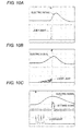
- Figs. 10A, 10B, and 10C are diagrams showing specific examples of the waveform shown in Fig. 9 .
- Fig. 10A is a diagram showing a waveform of a laser pulse when the number of pulses included in a group of pulses is 1 and a waveform of an electric signal after the integration.
- Fig. 10B is a diagram showing a waveform of a laser pulse when the number of pulses included in a group of pulses is 20 and a waveform of an electric signal after the integration
- Fig. 10C is a waveform diagram for describing timing of AD conversion performed on the signal waveform after the integration and amplification.
- the peak values of the laser pulse waveforms are evaluated by the voltage range and the ratio of the peak value of the laser light waveform shown in Fig. 10A and the peak value of the laser light waveform shown in Fig. 10B is about 5 : 2. That is, the peak value of the laser pulse waveform shown in Fig. 10A is about 2.5 times (according to the evaluation made by voltage range) the peak value of the laser pulse waveform shown in Fig. 10B . That corresponds to the fact that the peak value of the laser pulse shown in Fig. 10A is about 7 times the peak value of the laser pulse shown in Fig. 10B .
- the electric signal shown in Fig. 10A and the electric signal shown in Fig. 10B have almost the same peak value.
- Fig. 11 is a diagram showing the relationship between the amplitude of a signal which is input to an AD converter circuit 34 and the gain of the PGA 33.
- the gain of the PGA 33 increases stepwise as the repetition frequency increases.
- the frequencies f1 to f5 indicate the repetition frequencies when the gain is switched. That change of gain is achieved by a gain setting signal sent from the signal processing circuit 40 to the PGA 33.
- the light amplifier further includes a variable gain amplifier (PGA 33) for amplifying the output signal from the integration circuit 32 to provide the output signal for the AD converter circuit 34.
- the signal processing circuit 40 causes the gain of the PGA 33 to change according to the repetition frequency of the group of pulses to be generated during the emission period. Accordingly, the power of the group of output light pulses can be detected even when the repetition frequency changes widely.
- Fig. 13 is a configuration diagram of the laser processing device according to Embodiment 2.
- a laser processing device 101 includes a light amplifier constituted of a two stage fiber amplifier.
- the laser processing device according to Embodiment 2 is different from the laser processing device according to Embodiment 1.
- the laser processing device 101 is different from the laser processing device 100 in further including a coupler 7, a light amplifying fiber 8, exciting LDs 9A and 9B, a combiner 10, an isolator 11, a light receiving element 17, a peak value detector 18, and a driver 23.
- the exciting LDs 9A and 9B are driven by the driver 23.
- the driver 23 is controlled by the control device 20.
- the light amplifying fiber 8 amplifies the laser light from the coupler 7 by the laser lights from the exciting LDs 9A and 9B. That is, the laser light from the coupler 7 is the seed light and the laser lights from the exciting LDs 9A, 9B are excitation lights.
- the power of the excitation lights emitted from the exciting LDs 9A and 9B decreases in the preliminary excitation period and increases in the main excitation period.
- the isolator 11 allows the laser light output from the light amplifying fiber 8 to pass while blocking the laser light returning to the light amplifying fiber 8.
- the light receiving element 17 receives the light pulse from the coupler 7 and outputs a signal indicating the strength of the light pulse.
- the peak value detector 18 detects the peak value of the light pulse by the signal from the light receiving element 17. The peak value detected by the peak value detector 18 is sent to the control device 20.
- the control device 20 controls the driver 22 based on the peak value of the pulses detected by the light receiving element 17 and the peak value detector 18. Accordingly, the pulse emitted from the light amplifying fiber 1 can be controlled to make the peak values of the first pulses and the final pulses of the group of pulses emitted from the light amplifying fiber 1 the same. Further, the control device 20 controls the driver 23 based on the peak value of the pulses detected by the light receiving element 15 and the peak value detector 16.
- the pulse emitted from the light amplifying fiber 8 can be controlled to make the peak values of the first pulses and the final pulses of the plurality of pulses emitted from the final amplifying stage, i.e., the light amplifying fiber 8, the same. Since the controlling method according to Embodiment 1 can be applied to the method for controlling the pulse emitted from the light amplifying fiber 8, it is not described again in detail below.
- the number of the exciting LDs provided for each amplifying stage is not limited to those shown in Figs. 1 and 13 , and any number of exciting LDs may be set.
Landscapes
- Physics & Mathematics (AREA)
- Optics & Photonics (AREA)
- Electromagnetism (AREA)
- Engineering & Computer Science (AREA)
- Plasma & Fusion (AREA)
- Mechanical Engineering (AREA)
- Lasers (AREA)
- Laser Beam Processing (AREA)
Applications Claiming Priority (1)
| Application Number | Priority Date | Filing Date | Title |
|---|---|---|---|
| JP2011118040A JP5879747B2 (ja) | 2011-05-26 | 2011-05-26 | 光増幅装置およびレーザ加工装置 |
Publications (3)
| Publication Number | Publication Date |
|---|---|
| EP2528173A2 true EP2528173A2 (de) | 2012-11-28 |
| EP2528173A3 EP2528173A3 (de) | 2014-02-12 |
| EP2528173B1 EP2528173B1 (de) | 2017-03-29 |
Family
ID=46197018
Family Applications (1)
| Application Number | Title | Priority Date | Filing Date |
|---|---|---|---|
| EP12168489.8A Active EP2528173B1 (de) | 2011-05-26 | 2012-05-18 | Lichtverstärkungs- und Laserverarbeitungsvorrichtung |
Country Status (4)
| Country | Link |
|---|---|
| US (1) | US9025240B2 (de) |
| EP (1) | EP2528173B1 (de) |
| JP (1) | JP5879747B2 (de) |
| CN (1) | CN102801089B (de) |
Cited By (1)
| Publication number | Priority date | Publication date | Assignee | Title |
|---|---|---|---|---|
| CN103433621A (zh) * | 2013-07-29 | 2013-12-11 | 燕山大学 | 一种激光切割头工作状态的切换装置及方法 |
Families Citing this family (11)
| Publication number | Priority date | Publication date | Assignee | Title |
|---|---|---|---|---|
| WO2016143071A1 (ja) * | 2015-03-10 | 2016-09-15 | 国立大学法人 東京大学 | 固体レーザ装置、ファイバ増幅器システム、および固体レーザシステム |
| WO2017149712A1 (ja) | 2016-03-02 | 2017-09-08 | ギガフォトン株式会社 | レーザ装置及び極端紫外光生成システム |
| JP2018020372A (ja) * | 2016-08-07 | 2018-02-08 | 日本電産コパル株式会社 | レーザーマーキング装置 |
| JP2018174206A (ja) * | 2017-03-31 | 2018-11-08 | 株式会社フジクラ | レーザ装置 |
| US11081852B2 (en) * | 2017-04-24 | 2021-08-03 | Cymer, Llc | Laser light energy and dose control using repetition rate based gain estimators |
| CN108926340B (zh) * | 2017-05-23 | 2023-04-28 | 松下知识产权经营株式会社 | 计测装置 |
| KR102084558B1 (ko) * | 2017-09-22 | 2020-03-05 | 미쓰비시덴키 가부시키가이샤 | 레이저 가공 장치 |
| CN108390246B (zh) * | 2018-04-28 | 2024-10-15 | 无锡源清瑞光激光科技有限公司 | 一种模块化合束的准连续光纤激光器 |
| JP7441780B2 (ja) * | 2020-12-21 | 2024-03-01 | 浜松ホトニクス株式会社 | 光パルス生成装置及び光パルス生成方法 |
| JP7558885B2 (ja) * | 2021-05-12 | 2024-10-01 | 日本発條株式会社 | レーザ溶接装置と、レーザ溶接方法 |
| CN115635190A (zh) * | 2022-05-13 | 2023-01-24 | 日本发条株式会社 | 激光焊接设备和激光焊接方法 |
Citations (2)
| Publication number | Priority date | Publication date | Assignee | Title |
|---|---|---|---|---|
| JP2010010274A (ja) | 2008-06-25 | 2010-01-14 | Miyachi Technos Corp | レーザ加工装置 |
| JP2010171131A (ja) | 2009-01-21 | 2010-08-05 | Omron Corp | レーザ光源装置およびレーザ加工装置 |
Family Cites Families (18)
| Publication number | Priority date | Publication date | Assignee | Title |
|---|---|---|---|---|
| IL91240A (en) | 1989-08-07 | 1994-07-31 | Quick Tech Ltd | Pulsed laser apparatus and systems and techniques for its operation |
| JPH0477631A (ja) * | 1990-07-20 | 1992-03-11 | Mitsui Petrochem Ind Ltd | レーザ発振出力検出装置 |
| JPH08278796A (ja) * | 1995-04-10 | 1996-10-22 | Fujitsu Ten Ltd | 音声処理装置 |
| US5982790A (en) | 1997-01-16 | 1999-11-09 | Lightwave Electronics Corporation | System for reducing pulse-to-pulse energy variation in a pulsed laser |
| JP3407655B2 (ja) * | 1998-05-06 | 2003-05-19 | 株式会社デンソー | レーザ溶接監視方法 |
| WO2001020733A1 (en) * | 1999-09-10 | 2001-03-22 | Nikon Corporation | Light source and wavelength stabilization control method, exposure apparatus and exposure method, method for producing exposure apparatus, and device manufacturing method and device |
| JP2001345245A (ja) * | 2000-05-31 | 2001-12-14 | Nikon Corp | 露光方法及び露光装置並びにデバイス製造方法 |
| ATE553520T1 (de) | 2003-02-14 | 2012-04-15 | Univ Heidelberg | Verfahren zur erzeugung von mindestens ein puls und/oder einer pulssequenz mit kontrollierbaren parametern |
| US7103077B2 (en) | 2004-04-29 | 2006-09-05 | 20/10 Perfect Vision Optische Geraete Gmbh | System and method for measuring and controlling an energy of an ultra-short pulse of a laser beam |
| JP2006157652A (ja) * | 2004-11-30 | 2006-06-15 | Matsushita Electric Ind Co Ltd | 受信装置 |
| JP5203573B2 (ja) * | 2006-03-23 | 2013-06-05 | ミヤチテクノス株式会社 | レーザ加工装置 |
| JP2009141109A (ja) * | 2007-12-06 | 2009-06-25 | Furukawa Electric Co Ltd:The | 光デバイスの制御方法および光モジュール |
| EP2071682A1 (de) | 2007-12-13 | 2009-06-17 | Trumpf Laser Marking Systems AG | Verfahren zur Erstpulsoptimierung in gütegeschalteten Festkörperlasern sowie gütegeschalteter Festkörperlaser |
| JP5107732B2 (ja) * | 2008-01-22 | 2012-12-26 | 芝浦メカトロニクス株式会社 | レーザ発振装置およびレーザ発振方法 |
| JP2009248157A (ja) * | 2008-04-08 | 2009-10-29 | Miyachi Technos Corp | レーザ加工方法及びレーザ加工装置 |
| JP2010016257A (ja) * | 2008-07-04 | 2010-01-21 | Panasonic Corp | レーザ駆動装置 |
| JP5546119B2 (ja) | 2008-11-14 | 2014-07-09 | 株式会社アマダミヤチ | ファイバレーザ加工装置及びファイバレーザ加工方法 |
| JP4647696B2 (ja) | 2009-07-07 | 2011-03-09 | 株式会社フジクラ | ファイバレーザ装置 |
-
2011
- 2011-05-26 JP JP2011118040A patent/JP5879747B2/ja active Active
-
2012
- 2012-05-10 US US13/468,432 patent/US9025240B2/en active Active
- 2012-05-11 CN CN201210147641.0A patent/CN102801089B/zh not_active Expired - Fee Related
- 2012-05-18 EP EP12168489.8A patent/EP2528173B1/de active Active
Patent Citations (2)
| Publication number | Priority date | Publication date | Assignee | Title |
|---|---|---|---|---|
| JP2010010274A (ja) | 2008-06-25 | 2010-01-14 | Miyachi Technos Corp | レーザ加工装置 |
| JP2010171131A (ja) | 2009-01-21 | 2010-08-05 | Omron Corp | レーザ光源装置およびレーザ加工装置 |
Cited By (1)
| Publication number | Priority date | Publication date | Assignee | Title |
|---|---|---|---|---|
| CN103433621A (zh) * | 2013-07-29 | 2013-12-11 | 燕山大学 | 一种激光切割头工作状态的切换装置及方法 |
Also Published As
| Publication number | Publication date |
|---|---|
| US20120300289A1 (en) | 2012-11-29 |
| JP5879747B2 (ja) | 2016-03-08 |
| CN102801089A (zh) | 2012-11-28 |
| CN102801089B (zh) | 2014-12-24 |
| US9025240B2 (en) | 2015-05-05 |
| JP2012248614A (ja) | 2012-12-13 |
| EP2528173A3 (de) | 2014-02-12 |
| EP2528173B1 (de) | 2017-03-29 |
Similar Documents
| Publication | Publication Date | Title |
|---|---|---|
| EP2528173B1 (de) | Lichtverstärkungs- und Laserverarbeitungsvorrichtung | |
| EP2528172B1 (de) | Lichtverstärkungs- und Laserverarbeitungsvorrichtung | |
| CN102189330B (zh) | 激光加工装置 | |
| US9755397B2 (en) | Light amplifying device and laser processing apparatus | |
| JP2015503856A (ja) | 所定の出力パルスプロファイルを出射するパルスレーザ源のための方法及びシステム | |
| JP6345348B2 (ja) | 高ピークパワーのパルスバースト又は他の時間変化するレーザー出力波形の生成をサポートするようポンプパワーを時間的に凝縮する方法及び装置 | |
| US10038296B2 (en) | Light amplification device and laser processing device | |
| TWI589080B (zh) | 雷射裝置及雷射加工機 | |
| JP5918975B2 (ja) | Mopa方式レーザ光源装置およびmopa方式レーザ制御方法 | |
| US8867123B2 (en) | High-power pulsed light generator | |
| JP2022121108A (ja) | レーザ電子光発生装置およびレーザ光源装置 | |
| JP6276969B2 (ja) | 増幅用光ファイバのストークス光検出方法、及び、これを用いたファイバレーザ装置 | |
| CN210744444U (zh) | 一种多脉冲的激光雷达发生装置、系统及激光雷达 | |
| JP2890654B2 (ja) | 分布型光ファイバー温度センサー | |
| WO2024024388A1 (ja) | レーザ加工装置、レーザ加工装置の制御方法およびプログラム | |
| JP2013012534A (ja) | レーザ発振器、レーザ発振器の出力制御方法、及びレーザ加工装置 | |
| JPH0846272A (ja) | パルス光源 |
Legal Events
| Date | Code | Title | Description |
|---|---|---|---|
| PUAI | Public reference made under article 153(3) epc to a published international application that has entered the european phase |
Free format text: ORIGINAL CODE: 0009012 |
|
| AK | Designated contracting states |
Kind code of ref document: A2 Designated state(s): AL AT BE BG CH CY CZ DE DK EE ES FI FR GB GR HR HU IE IS IT LI LT LU LV MC MK MT NL NO PL PT RO RS SE SI SK SM TR |
|
| AX | Request for extension of the european patent |
Extension state: BA ME |
|
| PUAL | Search report despatched |
Free format text: ORIGINAL CODE: 0009013 |
|
| RIC1 | Information provided on ipc code assigned before grant |
Ipc: B23K 26/06 20060101ALN20140102BHEP Ipc: H01S 3/067 20060101AFI20140102BHEP Ipc: H01S 3/13 20060101ALN20140102BHEP Ipc: H01S 3/091 20060101ALN20140102BHEP Ipc: H01S 3/131 20060101ALI20140102BHEP Ipc: H01S 3/10 20060101ALN20140102BHEP Ipc: H01S 3/0941 20060101ALN20140102BHEP |
|
| AK | Designated contracting states |
Kind code of ref document: A3 Designated state(s): AL AT BE BG CH CY CZ DE DK EE ES FI FR GB GR HR HU IE IS IT LI LT LU LV MC MK MT NL NO PL PT RO RS SE SI SK SM TR |
|
| AX | Request for extension of the european patent |
Extension state: BA ME |
|
| 17P | Request for examination filed |
Effective date: 20140620 |
|
| RBV | Designated contracting states (corrected) |
Designated state(s): AL AT BE BG CH CY CZ DE DK EE ES FI FR GB GR HR HU IE IS IT LI LT LU LV MC MK MT NL NO PL PT RO RS SE SI SK SM TR |
|
| REG | Reference to a national code |
Ref country code: DE Ref legal event code: R079 Ref document number: 602012030377 Country of ref document: DE Free format text: PREVIOUS MAIN CLASS: H01S0003131000 Ipc: H01S0003067000 |
|
| GRAP | Despatch of communication of intention to grant a patent |
Free format text: ORIGINAL CODE: EPIDOSNIGR1 |
|
| STAA | Information on the status of an ep patent application or granted ep patent |
Free format text: STATUS: GRANT OF PATENT IS INTENDED |
|
| RIC1 | Information provided on ipc code assigned before grant |
Ipc: H01S 3/10 20060101ALN20161020BHEP Ipc: H01S 3/131 20060101ALI20161020BHEP Ipc: B23K 26/0622 20140101ALN20161020BHEP Ipc: H01S 3/067 20060101AFI20161020BHEP Ipc: H01S 3/13 20060101ALN20161020BHEP Ipc: H01S 3/094 20060101ALN20161020BHEP Ipc: H01S 3/0941 20060101ALN20161020BHEP Ipc: H01S 3/091 20060101ALN20161020BHEP |
|
| INTG | Intention to grant announced |
Effective date: 20161111 |
|
| RIN1 | Information on inventor provided before grant (corrected) |
Inventor name: OGAKI, TATSUO |
|
| GRAS | Grant fee paid |
Free format text: ORIGINAL CODE: EPIDOSNIGR3 |
|
| GRAA | (expected) grant |
Free format text: ORIGINAL CODE: 0009210 |
|
| STAA | Information on the status of an ep patent application or granted ep patent |
Free format text: STATUS: THE PATENT HAS BEEN GRANTED |
|
| AK | Designated contracting states |
Kind code of ref document: B1 Designated state(s): AL AT BE BG CH CY CZ DE DK EE ES FI FR GB GR HR HU IE IS IT LI LT LU LV MC MK MT NL NO PL PT RO RS SE SI SK SM TR |
|
| REG | Reference to a national code |
Ref country code: GB Ref legal event code: FG4D |
|
| REG | Reference to a national code |
Ref country code: CH Ref legal event code: EP |
|
| REG | Reference to a national code |
Ref country code: AT Ref legal event code: REF Ref document number: 880563 Country of ref document: AT Kind code of ref document: T Effective date: 20170415 |
|
| REG | Reference to a national code |
Ref country code: IE Ref legal event code: FG4D |
|
| REG | Reference to a national code |
Ref country code: DE Ref legal event code: R096 Ref document number: 602012030377 Country of ref document: DE |
|
| PG25 | Lapsed in a contracting state [announced via postgrant information from national office to epo] |
Ref country code: HR Free format text: LAPSE BECAUSE OF FAILURE TO SUBMIT A TRANSLATION OF THE DESCRIPTION OR TO PAY THE FEE WITHIN THE PRESCRIBED TIME-LIMIT Effective date: 20170329 Ref country code: NO Free format text: LAPSE BECAUSE OF FAILURE TO SUBMIT A TRANSLATION OF THE DESCRIPTION OR TO PAY THE FEE WITHIN THE PRESCRIBED TIME-LIMIT Effective date: 20170629 Ref country code: GR Free format text: LAPSE BECAUSE OF FAILURE TO SUBMIT A TRANSLATION OF THE DESCRIPTION OR TO PAY THE FEE WITHIN THE PRESCRIBED TIME-LIMIT Effective date: 20170630 Ref country code: FI Free format text: LAPSE BECAUSE OF FAILURE TO SUBMIT A TRANSLATION OF THE DESCRIPTION OR TO PAY THE FEE WITHIN THE PRESCRIBED TIME-LIMIT Effective date: 20170329 Ref country code: LT Free format text: LAPSE BECAUSE OF FAILURE TO SUBMIT A TRANSLATION OF THE DESCRIPTION OR TO PAY THE FEE WITHIN THE PRESCRIBED TIME-LIMIT Effective date: 20170329 |
|
| REG | Reference to a national code |
Ref country code: NL Ref legal event code: MP Effective date: 20170329 |
|
| REG | Reference to a national code |
Ref country code: AT Ref legal event code: MK05 Ref document number: 880563 Country of ref document: AT Kind code of ref document: T Effective date: 20170329 |
|
| PG25 | Lapsed in a contracting state [announced via postgrant information from national office to epo] |
Ref country code: RS Free format text: LAPSE BECAUSE OF FAILURE TO SUBMIT A TRANSLATION OF THE DESCRIPTION OR TO PAY THE FEE WITHIN THE PRESCRIBED TIME-LIMIT Effective date: 20170329 Ref country code: LU Free format text: LAPSE BECAUSE OF NON-PAYMENT OF DUE FEES Effective date: 20170531 Ref country code: LV Free format text: LAPSE BECAUSE OF FAILURE TO SUBMIT A TRANSLATION OF THE DESCRIPTION OR TO PAY THE FEE WITHIN THE PRESCRIBED TIME-LIMIT Effective date: 20170329 Ref country code: SE Free format text: LAPSE BECAUSE OF FAILURE TO SUBMIT A TRANSLATION OF THE DESCRIPTION OR TO PAY THE FEE WITHIN THE PRESCRIBED TIME-LIMIT Effective date: 20170329 Ref country code: BG Free format text: LAPSE BECAUSE OF FAILURE TO SUBMIT A TRANSLATION OF THE DESCRIPTION OR TO PAY THE FEE WITHIN THE PRESCRIBED TIME-LIMIT Effective date: 20170629 |
|
| PG25 | Lapsed in a contracting state [announced via postgrant information from national office to epo] |
Ref country code: NL Free format text: LAPSE BECAUSE OF FAILURE TO SUBMIT A TRANSLATION OF THE DESCRIPTION OR TO PAY THE FEE WITHIN THE PRESCRIBED TIME-LIMIT Effective date: 20170329 |
|
| PG25 | Lapsed in a contracting state [announced via postgrant information from national office to epo] |
Ref country code: IT Free format text: LAPSE BECAUSE OF FAILURE TO SUBMIT A TRANSLATION OF THE DESCRIPTION OR TO PAY THE FEE WITHIN THE PRESCRIBED TIME-LIMIT Effective date: 20170329 Ref country code: EE Free format text: LAPSE BECAUSE OF FAILURE TO SUBMIT A TRANSLATION OF THE DESCRIPTION OR TO PAY THE FEE WITHIN THE PRESCRIBED TIME-LIMIT Effective date: 20170329 Ref country code: AT Free format text: LAPSE BECAUSE OF FAILURE TO SUBMIT A TRANSLATION OF THE DESCRIPTION OR TO PAY THE FEE WITHIN THE PRESCRIBED TIME-LIMIT Effective date: 20170329 Ref country code: RO Free format text: LAPSE BECAUSE OF FAILURE TO SUBMIT A TRANSLATION OF THE DESCRIPTION OR TO PAY THE FEE WITHIN THE PRESCRIBED TIME-LIMIT Effective date: 20170329 Ref country code: SK Free format text: LAPSE BECAUSE OF FAILURE TO SUBMIT A TRANSLATION OF THE DESCRIPTION OR TO PAY THE FEE WITHIN THE PRESCRIBED TIME-LIMIT Effective date: 20170329 Ref country code: CZ Free format text: LAPSE BECAUSE OF FAILURE TO SUBMIT A TRANSLATION OF THE DESCRIPTION OR TO PAY THE FEE WITHIN THE PRESCRIBED TIME-LIMIT Effective date: 20170329 Ref country code: ES Free format text: LAPSE BECAUSE OF FAILURE TO SUBMIT A TRANSLATION OF THE DESCRIPTION OR TO PAY THE FEE WITHIN THE PRESCRIBED TIME-LIMIT Effective date: 20170329 |
|
| PG25 | Lapsed in a contracting state [announced via postgrant information from national office to epo] |
Ref country code: PT Free format text: LAPSE BECAUSE OF FAILURE TO SUBMIT A TRANSLATION OF THE DESCRIPTION OR TO PAY THE FEE WITHIN THE PRESCRIBED TIME-LIMIT Effective date: 20170731 Ref country code: IS Free format text: LAPSE BECAUSE OF FAILURE TO SUBMIT A TRANSLATION OF THE DESCRIPTION OR TO PAY THE FEE WITHIN THE PRESCRIBED TIME-LIMIT Effective date: 20170729 Ref country code: PL Free format text: LAPSE BECAUSE OF FAILURE TO SUBMIT A TRANSLATION OF THE DESCRIPTION OR TO PAY THE FEE WITHIN THE PRESCRIBED TIME-LIMIT Effective date: 20170329 Ref country code: SM Free format text: LAPSE BECAUSE OF FAILURE TO SUBMIT A TRANSLATION OF THE DESCRIPTION OR TO PAY THE FEE WITHIN THE PRESCRIBED TIME-LIMIT Effective date: 20170329 |
|
| REG | Reference to a national code |
Ref country code: CH Ref legal event code: PL |
|
| REG | Reference to a national code |
Ref country code: DE Ref legal event code: R097 Ref document number: 602012030377 Country of ref document: DE |
|
| PG25 | Lapsed in a contracting state [announced via postgrant information from national office to epo] |
Ref country code: MC Free format text: LAPSE BECAUSE OF FAILURE TO SUBMIT A TRANSLATION OF THE DESCRIPTION OR TO PAY THE FEE WITHIN THE PRESCRIBED TIME-LIMIT Effective date: 20170329 Ref country code: DK Free format text: LAPSE BECAUSE OF FAILURE TO SUBMIT A TRANSLATION OF THE DESCRIPTION OR TO PAY THE FEE WITHIN THE PRESCRIBED TIME-LIMIT Effective date: 20170329 |
|
| PLBE | No opposition filed within time limit |
Free format text: ORIGINAL CODE: 0009261 |
|
| STAA | Information on the status of an ep patent application or granted ep patent |
Free format text: STATUS: NO OPPOSITION FILED WITHIN TIME LIMIT |
|
| REG | Reference to a national code |
Ref country code: IE Ref legal event code: MM4A |
|
| GBPC | Gb: european patent ceased through non-payment of renewal fee |
Effective date: 20170629 |
|
| PG25 | Lapsed in a contracting state [announced via postgrant information from national office to epo] |
Ref country code: LI Free format text: LAPSE BECAUSE OF NON-PAYMENT OF DUE FEES Effective date: 20170531 Ref country code: CH Free format text: LAPSE BECAUSE OF NON-PAYMENT OF DUE FEES Effective date: 20170531 |
|
| REG | Reference to a national code |
Ref country code: FR Ref legal event code: ST Effective date: 20180131 |
|
| 26N | No opposition filed |
Effective date: 20180103 |
|
| PG25 | Lapsed in a contracting state [announced via postgrant information from national office to epo] |
Ref country code: LU Free format text: LAPSE BECAUSE OF NON-PAYMENT OF DUE FEES Effective date: 20170518 |
|
| REG | Reference to a national code |
Ref country code: BE Ref legal event code: MM Effective date: 20170531 |
|
| PG25 | Lapsed in a contracting state [announced via postgrant information from national office to epo] |
Ref country code: IE Free format text: LAPSE BECAUSE OF NON-PAYMENT OF DUE FEES Effective date: 20170518 Ref country code: GB Free format text: LAPSE BECAUSE OF NON-PAYMENT OF DUE FEES Effective date: 20170629 |
|
| PG25 | Lapsed in a contracting state [announced via postgrant information from national office to epo] |
Ref country code: FR Free format text: LAPSE BECAUSE OF NON-PAYMENT OF DUE FEES Effective date: 20170531 Ref country code: SI Free format text: LAPSE BECAUSE OF FAILURE TO SUBMIT A TRANSLATION OF THE DESCRIPTION OR TO PAY THE FEE WITHIN THE PRESCRIBED TIME-LIMIT Effective date: 20170329 |
|
| PG25 | Lapsed in a contracting state [announced via postgrant information from national office to epo] |
Ref country code: BE Free format text: LAPSE BECAUSE OF NON-PAYMENT OF DUE FEES Effective date: 20170531 |
|
| PG25 | Lapsed in a contracting state [announced via postgrant information from national office to epo] |
Ref country code: MT Free format text: LAPSE BECAUSE OF NON-PAYMENT OF DUE FEES Effective date: 20170518 |
|
| PG25 | Lapsed in a contracting state [announced via postgrant information from national office to epo] |
Ref country code: HU Free format text: LAPSE BECAUSE OF FAILURE TO SUBMIT A TRANSLATION OF THE DESCRIPTION OR TO PAY THE FEE WITHIN THE PRESCRIBED TIME-LIMIT; INVALID AB INITIO Effective date: 20120518 |
|
| PG25 | Lapsed in a contracting state [announced via postgrant information from national office to epo] |
Ref country code: CY Free format text: LAPSE BECAUSE OF NON-PAYMENT OF DUE FEES Effective date: 20170329 |
|
| PG25 | Lapsed in a contracting state [announced via postgrant information from national office to epo] |
Ref country code: MK Free format text: LAPSE BECAUSE OF FAILURE TO SUBMIT A TRANSLATION OF THE DESCRIPTION OR TO PAY THE FEE WITHIN THE PRESCRIBED TIME-LIMIT Effective date: 20170329 |
|
| PG25 | Lapsed in a contracting state [announced via postgrant information from national office to epo] |
Ref country code: TR Free format text: LAPSE BECAUSE OF FAILURE TO SUBMIT A TRANSLATION OF THE DESCRIPTION OR TO PAY THE FEE WITHIN THE PRESCRIBED TIME-LIMIT Effective date: 20170329 |
|
| PG25 | Lapsed in a contracting state [announced via postgrant information from national office to epo] |
Ref country code: AL Free format text: LAPSE BECAUSE OF FAILURE TO SUBMIT A TRANSLATION OF THE DESCRIPTION OR TO PAY THE FEE WITHIN THE PRESCRIBED TIME-LIMIT Effective date: 20170329 |
|
| PGFP | Annual fee paid to national office [announced via postgrant information from national office to epo] |
Ref country code: DE Payment date: 20250519 Year of fee payment: 14 |