EP2526409B1 - Site based quantification of substrate topography and its relation to lithography defocus and overlay - Google Patents
Site based quantification of substrate topography and its relation to lithography defocus and overlay Download PDFInfo
- Publication number
- EP2526409B1 EP2526409B1 EP11732096.0A EP11732096A EP2526409B1 EP 2526409 B1 EP2526409 B1 EP 2526409B1 EP 11732096 A EP11732096 A EP 11732096A EP 2526409 B1 EP2526409 B1 EP 2526409B1
- Authority
- EP
- European Patent Office
- Prior art keywords
- substrate
- back surface
- lithography
- wafer
- data
- Prior art date
- Legal status (The legal status is an assumption and is not a legal conclusion. Google has not performed a legal analysis and makes no representation as to the accuracy of the status listed.)
- Active
Links
Images


Classifications
-
- G—PHYSICS
- G01—MEASURING; TESTING
- G01B—MEASURING LENGTH, THICKNESS OR SIMILAR LINEAR DIMENSIONS; MEASURING ANGLES; MEASURING AREAS; MEASURING IRREGULARITIES OF SURFACES OR CONTOURS
- G01B11/00—Measuring arrangements characterised by the use of optical techniques
- G01B11/24—Measuring arrangements characterised by the use of optical techniques for measuring contours or curvatures
-
- G—PHYSICS
- G01—MEASURING; TESTING
- G01N—INVESTIGATING OR ANALYSING MATERIALS BY DETERMINING THEIR CHEMICAL OR PHYSICAL PROPERTIES
- G01N21/00—Investigating or analysing materials by the use of optical means, i.e. using sub-millimetre waves, infrared, visible or ultraviolet light
- G01N21/84—Systems specially adapted for particular applications
- G01N21/88—Investigating the presence of flaws or contamination
- G01N21/95—Investigating the presence of flaws or contamination characterised by the material or shape of the object to be examined
- G01N21/9501—Semiconductor wafers
-
- G—PHYSICS
- G03—PHOTOGRAPHY; CINEMATOGRAPHY; ANALOGOUS TECHNIQUES USING WAVES OTHER THAN OPTICAL WAVES; ELECTROGRAPHY; HOLOGRAPHY
- G03F—PHOTOMECHANICAL PRODUCTION OF TEXTURED OR PATTERNED SURFACES, e.g. FOR PRINTING, FOR PROCESSING OF SEMICONDUCTOR DEVICES; MATERIALS THEREFOR; ORIGINALS THEREFOR; APPARATUS SPECIALLY ADAPTED THEREFOR
- G03F7/00—Photomechanical, e.g. photolithographic, production of textured or patterned surfaces, e.g. printing surfaces; Materials therefor, e.g. comprising photoresists; Apparatus specially adapted therefor
- G03F7/70—Microphotolithographic exposure; Apparatus therefor
- G03F7/70483—Information management; Active and passive control; Testing; Wafer monitoring, e.g. pattern monitoring
- G03F7/70491—Information management, e.g. software; Active and passive control, e.g. details of controlling exposure processes or exposure tool monitoring processes
- G03F7/705—Modelling or simulating from physical phenomena up to complete wafer processes or whole workflow in wafer productions
-
- G—PHYSICS
- G03—PHOTOGRAPHY; CINEMATOGRAPHY; ANALOGOUS TECHNIQUES USING WAVES OTHER THAN OPTICAL WAVES; ELECTROGRAPHY; HOLOGRAPHY
- G03F—PHOTOMECHANICAL PRODUCTION OF TEXTURED OR PATTERNED SURFACES, e.g. FOR PRINTING, FOR PROCESSING OF SEMICONDUCTOR DEVICES; MATERIALS THEREFOR; ORIGINALS THEREFOR; APPARATUS SPECIALLY ADAPTED THEREFOR
- G03F7/00—Photomechanical, e.g. photolithographic, production of textured or patterned surfaces, e.g. printing surfaces; Materials therefor, e.g. comprising photoresists; Apparatus specially adapted therefor
- G03F7/70—Microphotolithographic exposure; Apparatus therefor
- G03F7/70483—Information management; Active and passive control; Testing; Wafer monitoring, e.g. pattern monitoring
- G03F7/70605—Workpiece metrology
- G03F7/70616—Monitoring the printed patterns
- G03F7/70633—Overlay, i.e. relative alignment between patterns printed by separate exposures in different layers, or in the same layer in multiple exposures or stitching
-
- G—PHYSICS
- G03—PHOTOGRAPHY; CINEMATOGRAPHY; ANALOGOUS TECHNIQUES USING WAVES OTHER THAN OPTICAL WAVES; ELECTROGRAPHY; HOLOGRAPHY
- G03F—PHOTOMECHANICAL PRODUCTION OF TEXTURED OR PATTERNED SURFACES, e.g. FOR PRINTING, FOR PROCESSING OF SEMICONDUCTOR DEVICES; MATERIALS THEREFOR; ORIGINALS THEREFOR; APPARATUS SPECIALLY ADAPTED THEREFOR
- G03F7/00—Photomechanical, e.g. photolithographic, production of textured or patterned surfaces, e.g. printing surfaces; Materials therefor, e.g. comprising photoresists; Apparatus specially adapted therefor
- G03F7/70—Microphotolithographic exposure; Apparatus therefor
- G03F7/70483—Information management; Active and passive control; Testing; Wafer monitoring, e.g. pattern monitoring
- G03F7/70605—Workpiece metrology
- G03F7/70616—Monitoring the printed patterns
- G03F7/70641—Focus
-
- G—PHYSICS
- G03—PHOTOGRAPHY; CINEMATOGRAPHY; ANALOGOUS TECHNIQUES USING WAVES OTHER THAN OPTICAL WAVES; ELECTROGRAPHY; HOLOGRAPHY
- G03F—PHOTOMECHANICAL PRODUCTION OF TEXTURED OR PATTERNED SURFACES, e.g. FOR PRINTING, FOR PROCESSING OF SEMICONDUCTOR DEVICES; MATERIALS THEREFOR; ORIGINALS THEREFOR; APPARATUS SPECIALLY ADAPTED THEREFOR
- G03F7/00—Photomechanical, e.g. photolithographic, production of textured or patterned surfaces, e.g. printing surfaces; Materials therefor, e.g. comprising photoresists; Apparatus specially adapted therefor
- G03F7/70—Microphotolithographic exposure; Apparatus therefor
- G03F7/70483—Information management; Active and passive control; Testing; Wafer monitoring, e.g. pattern monitoring
- G03F7/70605—Workpiece metrology
- G03F7/70616—Monitoring the printed patterns
- G03F7/7065—Defects, e.g. optical inspection of patterned layer for defects
-
- G—PHYSICS
- G03—PHOTOGRAPHY; CINEMATOGRAPHY; ANALOGOUS TECHNIQUES USING WAVES OTHER THAN OPTICAL WAVES; ELECTROGRAPHY; HOLOGRAPHY
- G03F—PHOTOMECHANICAL PRODUCTION OF TEXTURED OR PATTERNED SURFACES, e.g. FOR PRINTING, FOR PROCESSING OF SEMICONDUCTOR DEVICES; MATERIALS THEREFOR; ORIGINALS THEREFOR; APPARATUS SPECIALLY ADAPTED THEREFOR
- G03F7/00—Photomechanical, e.g. photolithographic, production of textured or patterned surfaces, e.g. printing surfaces; Materials therefor, e.g. comprising photoresists; Apparatus specially adapted therefor
- G03F7/70—Microphotolithographic exposure; Apparatus therefor
- G03F7/70691—Handling of masks or workpieces
- G03F7/70783—Handling stress or warp of chucks, masks or workpieces, e.g. to compensate for imaging errors or considerations related to warpage of masks or workpieces due to their own weight
-
- G—PHYSICS
- G06—COMPUTING OR CALCULATING; COUNTING
- G06F—ELECTRIC DIGITAL DATA PROCESSING
- G06F30/00—Computer-aided design [CAD]
- G06F30/20—Design optimisation, verification or simulation
-
- G—PHYSICS
- G06—COMPUTING OR CALCULATING; COUNTING
- G06F—ELECTRIC DIGITAL DATA PROCESSING
- G06F30/00—Computer-aided design [CAD]
- G06F30/20—Design optimisation, verification or simulation
- G06F30/23—Design optimisation, verification or simulation using finite element methods [FEM] or finite difference methods [FDM]
-
- H—ELECTRICITY
- H01—ELECTRIC ELEMENTS
- H01L—SEMICONDUCTOR DEVICES NOT COVERED BY CLASS H10
- H01L22/00—Testing or measuring during manufacture or treatment; Reliability measurements, i.e. testing of parts without further processing to modify the parts as such; Structural arrangements therefor
- H01L22/10—Measuring as part of the manufacturing process
- H01L22/12—Measuring as part of the manufacturing process for structural parameters, e.g. thickness, line width, refractive index, temperature, warp, bond strength, defects, optical inspection, electrical measurement of structural dimensions, metallurgic measurement of diffusions
Definitions
- This invention relates to integrated circuit processing, and in particular to the characterization of wafer substrate topography and its relation to overlay and defocus errors in lithography.
- Wafer topography i.e., substrate geometry
- NT nanotopography
- the data representing these parameters have a high spatial resolution of about 0.2 mm.
- Shape is defined as the median surface of the substrate (as in the deviation of the median surface from a reference plane), generally in a free state, and is a low frequency component of the wafer. Shape is characterized by global metric such as warp and bow.
- Flatness is defined as the thickness variation of a substrate with the back surface assumed to be completely flat, and is characterized by metrics, which may be localized or site-based.
- Nanotopography is the high frequency component of the front and back surface of the substrate, defined as being in a spatial wavelength regime of 0.2-20 mm, and with a feature height of a few nanometers.
- NT may occur as point defects (e.g.,dimples, epi defects such as pins or crowns, bumps such as notches or lasermarks) or as line defects (e.g., saw marks from slicing, scratches, slip lines, dopant striation or other process signatures).
- the individual front/back surface nanotopography of a wafer substrate is typically obtained from the front/back topography by applying high pass filtering schemes such as Double Gaussian (DG) filtering to the topography data, which suppresses the low frequency components of the wafer topography.
- DG Double Gaussian
- the substrate NT parameters are seen to affect the lithography process, for example by contributing to defocus and overlay errors.
- corrections to distortions or other topographic features which may result in overlay or defocus errors are applied by the scanner on both a full wafer-level and a site-by-site basis.
- the most common linear scanner corrections (which includes both wafer level and site level) for overlay are: translation in x and y, rotation, and site-level magnification in xy and y.
- the corrections are typically calculated by minimizing the errors at target locations within the lithography sites using a process such as least squares.
- Scanner based linear corrections can generally correct for lower order linear components of the substrate geometry and other linear components which might result in overlay and defocus errors.
- the lithography scanner has limited capability to correct for features with spatial frequency less than 1/slit size of the lithography scanner.
- the NT which has spatial frequency less than 1/slit size may therefore result in Non-Correctable Errors (NCE).
- NCE Non-Correctable Errors
- US2004/185662 discloses a wafer flatness evaluation method includes measuring front and rear surface shapes of a wafer. The wafer front surface measured is divided into sites. Then, a flatness calculating method is selected according to a position of the site to be evaluated and flatness in the wafer surface is acquired.
- a methodology and system therefore is presented herein for quantifying the substrate NT and its effect on the lithography process parameters.
- This methodology utilizes a finite element model.
- the method for evaluating metrological characteristics of a semiconductor substrate is defined in claim 1.
- the system for evaluating metrological characteristics of a semiconductor substrate is defined in claim 9.
- the method and system described herein provides for the measurement and quantification of wafer NT relevant to lithography with appropriate metrics (such as Peak-to-Valley (PV) range and RMS), and the effect of the NT on such parameters as lithography defocus and overlay error.
- appropriate metrics such as Peak-to-Valley (PV) range and RMS
- the results obtained in this way enable the sorting and/or qualification of bare or patterned wafers for the process flow.
- Wafer qualification may be accomplished by comparing the quantified metric values to a user-determined threshold or cut-off, which may be determined at least in part by the process flow.
- a first requirement for developing a quantification methodology for determining the influence of wafer topographical aspects such as NT or shape on lithographic overlay/defocus is to accurately measure the wafer front and back surface topography. Wafer measurement with the wafer in a free state, where front and back surface can be measured simultaneously, is preferred, since it eliminates possible artifacts in the substrate topography data due to the interaction between the substrate and the chuck or other holding mechanism.
- a dimensional metrology tool such as WaferSight2 from KLA-Tencor provides the utility of measuring front-side and back-side topography, as well as thickness/flatness, simultaneously.
- This tool is described in K. Freischlad, S. Tang, and J. Grenfell, "Interferometry for wafer dimensional metrology", Proceedings of SPIE, 6672, 1 (2007 ).
- An aspect of the improved measurement methodology provided by this tool is that the substrate is measured in a free state, where the substrate is held vertically at only a few contact points, so that the topography of the front and back surface can be measured simultaneously.
- Use of the WaferSight2 tool enables refinement of quantification methodology for NT. Note that measurements of the wafer topography may be stored in computer memory, and computer-based analysis and/or modeling may be performed.
- the inventive quantification methodology is site-based, which generally implies localized.
- Prior methodologies for NT a surface-based quantity, provided one "average" or threshold curve for the entire wafer.
- flatness/thickness measurement and characterization, as well as shape measurement and characterization have been previously addressed by more sophisticated site-based methods, as described in PCT publication no. WO 2010/025334 , and in SEMI M49-0307, "Guide for specifying geometry measurement systems for silicon wafers for the 130 nm - 65 nm node technology", www.semi.org, 2004 .
- design rules get smaller, presently reaching approximately 22nm, the impact of high frequency NT features on lithography parameters such as defocus/overlay increases. Accordingly, it becomes increasingly important to refine the measurement quantification methodology for NT and to develop process-relevant metrics.
- Site-based measurement methods have two important advantages over whole-wafer averaging methods:
- An embodiment of the present NT quantification method calculates the substrate geometry in a way compatible with the calculation of defocus and overlay errors in each lithography field, also termed "sites". Therefore the substrate geometry may be quantified in the lithography field domain to correlate with the defocus and overlay.
- An embodiment of the present method uses the site-based quantification methodology, and utilizes a non-linear contact finite element modeling scheme to model the effects of the NT on In-Plane-Distortion (IPD), from which overlay can be derived.
- IPD In-Plane-Distortion
- Use of finite element modeling to model the effects of wafer shape distortion on overlay errors is described in the paper by K. Turner et al.
- a brief description of Finite element analysis is as follows: FEA consists of a computer model of a material or design that is stressed and analyzed for specific results. It is used in new product design, and existing product refinement. A company is able to verify a proposed design will be able to perform to the client's specifications prior to manufacturing or construction. Modifying an existing product or structure is utilized to qualify the product or structure for a new service condition. In case of structural failure, FEA may be used to help determine the design modifications to meet the new condition.
- FEA uses a complex system of points called nodes which make a grid called a mesh .
- This mesh is programmed to contain the material and structural properties which define how the structure will react to certain loading conditions. Nodes are assigned at a certain density throughout the material depending on the anticipated stress levels of a particular area. Regions which will receive large amounts of stress usually have a higher node density than those which experience little or no stress. Points of interest may consist of: fracture point of previously tested material, fillets, corners, complex detail, and high stress areas.
- the mesh acts like a spider web in that from each node, there extends a mesh element to each of the adjacent nodes. This web of vectors is what carries the material properties to the object, creating many elements. (Theory)
- a wide range of objective functions are available for minimization or maximization:
- FEA may be implemented using a commercially available modeling package such as ANSYS.
- the choice of inputs and outputs to/from the modeling package is critical in obtaining maximum utility from the modeling.
- the model is generated using a series of custom MATLAB scripts that read the high-density NT data files and construct the model geometry and mesh for the FE package.
- An embodiment of a method for quantifying substrate NT according to the above domain structure includes dividing the substrate surface into lithography fields (sites) and then quantifying the measured NT in each lithography field using an appropriate metric such as a range, deviation, or root mean square (RMS).
- an appropriate metric such as a range, deviation, or root mean square (RMS).
- the maximum magnitude of NT features may be quantified using a range metric, whereas to quantify the average high frequency NT, RMS may be utilized.
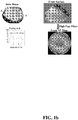
- Fig. 2 illustrates wafer 200 divided into lithography fields or sites 205. Within each site, substrate front and back surface filtered geometry data points 210 are taken with an exemplary density of 0.2 mm in x and y. The data may include NT and/or thickness data.
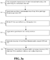
- step 300 topographic measurements are performed on the wafer front and back surfaces, the wafer being in a substantially free state.
- a high pass filter is applied to measurement of the front or back substrate surface.
- step 310 the remaining surface features, i.e., the high frequency geometry or NT, is divided into user-defined sites such as lithography sites.
- step 315 metric quantification is applied on a site-by-site basis.
- step 320 the data obtained in this way is input into the Finite Element model and out of plane distortions (OPD) and IPD are computed.
- OPD plane distortions
- step 325 data is output, and the OPD and IPD from step 320 are correlated to defocus and overlay respectively.
- Fig. 3b is a visual illustration of the flow diagram of Fig. 3a .
- FEA non-linear contact Finite Element Analysis
- the non-linear contact Finite Element Model models the interaction of the substrate back surface including NT with the chuck, e.g., lithography pins.
- the FEA can be used to model different parameters such as substrate shape. Depending on the parameter under study, the inputs to the model are varied, as described below.
- Fig. 4 illustrates the chucking of wafer 400 on chuck 405, with pins 410 contacting wafer back surface 415.
- Fig. 5 illustrates a high level diagram of a finite element model embodiment used herein.
- Wafer parameters 500 are a first input category to the finite element model 515.
- Wafer parameters include: a) Silicon material properties 502 (for example, modulus of elasticity, e.g., 150 Gpa, and Poissons ratio, 0.28), and b) substrate geometry divided into sites corresponding to lithography fields to result in site-based geometry 505.
- the wafer geometry includes front and back surface NT 507 and thickness 508.
- Chuck parameters 510 are a second input category, which may include chuck design 511 such as the pin top size (for example 0.2 x 0.2 mm), pin spacing (for example 2 mm), pressure (e.g., 80 kPa), and chuck ceramic material properties 513.
- chuck design 511 such as the pin top size (for example 0.2 x 0.2 mm), pin spacing (for example 2 mm), pressure (e.g., 80 kPa), and chuck ceramic material properties 513.
- Inputs to the finite element model are varied depending on the parameter under study.
- the model simulates the interaction of the wafer back surface NT with the lithography pin chuck and how it affects the front surface NT while the wafer is on the vacuum chuck (termed "post-chucking).
- the outputs of the finite element model include, on a site-by-site basis: out-of-plane distortion (OPD) 520, which is correlated with defocus 525 (a parameter described by leveling verification test (LVT) data.
- LVT leveling verification test
- IPD in-plane distortion
- Both defocus and overlay are observed at the lithography scanner and generally calculated at each lithography site.
- Post-processing 540 of the FE output data is performed to yield the calculated overlay error. Details of methods for calculating overlay are found in the paper by Turner et al.
- the outputs may also include the post-chucking front surface NT resulting from the interaction of the back surface NT with the lithography chuck.
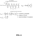
- Fig. 6 illustrates an analytical model for an assumed ideal sinusoidal back wafer surface. This model results from the fundamental mechanics of plate theory. The front surface topography is calculated assuming the back surface of the wafer is completely flattened by the vacuum chuck. There is excellent correlation between the FE model and the analytical model for NT spatial wavelengths of 2 mm and above: for shorter spatial wavelengths, complex shear deformations become important, which are included in the FE model but not in the analytical model. Therefore the two models diverge for the short spatial wavelengths. The correlation between the two models is further validation of the FE analysis.
- Fig. 7 shows exemplary FE modeling results of the effects of backside NT on frontside topography while chucked, for case 1 ( fig. 7a ) and case 2 ( fig. 7b ).
- the backside topography is smaller than the frontside topography before chucking, and in this case the peak-to-valley (PV) topography of the front surface while chucked is affected very little.
- the backside NT is larger than the front surface topography before chucking.
- the chucked front surface is greatly affected by the backside NT.
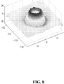
- An example of an often-encountered large PV backside NT feature is an epi pin defect (illustrated in Fig. 8 ), a topography feature caused during an epi deposition process.
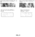
- Fig. 9 illustrates front side IPD (calculated using the FE model) corresponding to back surface NT.
- backside NT can be quantified and controlled, overlay errors can be reduced and yield improved. If, by way of example, 5% of lithography sites are over epi pin defects, large PV NT features which will result in IPD and overlay error (and lower yield), then the potential exists to improve yield by an equivalent amount by controlling the epi pin NT.
- the inventive methods or portions thereof may be computer-implemented.
- the computer system may include a processor (e.g. a processor core, a microprocessor, a computing device, etc), a main memory and a static memory, which communicate with each other via a bus.
- the machine may further include a display unit that may comprise a touch-screen, or a liquid crystal display (LCD), or a light emitting diode (LED) display, or a cathode ray tube (CRT).
- the computer system also may include a human input/output (I/O) device (e.g. a keyboard, an alphanumeric keypad, etc), a pointing device (e.g. a mouse, a touch screen, etc), a drive unit (e.g.
- I/O human input/output
- a disk drive unit e.g. a disk drive unit, a CD/DVD drive, a tangible computer readable removable media drive, an SSD storage device, etc
- a signal generation device e.g. a speaker, an audio output, etc
- a network interface device e.g. an Ethernet interface, a wired network interface, a wireless network interface, a propagated signal interface, etc.
- the drive unit may include a machine-readable medium on which is stored a set of instructions (i.e. software, firmware, middleware, etc) embodying any one, or all, of the methodologies described above.
- the set of instructions is also shown to reside, completely or at least partially, within the main memory and/or within the processor.
- the set of instructions may further be transmitted or received via the network interface device over the network bus.
- a machine-readable medium includes any mechanism for storing or transmitting information in a form readable by a machine (e.g. a computer).
- a machine-readable medium includes read-only memory (ROM); random access memory (RAM); magnetic disk storage media; optical storage media; flash memory devices; electrical, optical, acoustical or other form of propagated signals (e.g. carrier waves, infrared signals, digital signals, etc); or any other type of media suitable for storing or transmitting information.
- lithographic overlay accuracy must improve.
- a first step is quantification of chucking-induced IPD.
- the methodology and system disclosed herein provides lithography site-based quantification of backside NT and FE modeling of corresponding chucking-induced IPD and overlay error.
Landscapes
- Physics & Mathematics (AREA)
- General Physics & Mathematics (AREA)
- Engineering & Computer Science (AREA)
- Theoretical Computer Science (AREA)
- Computer Hardware Design (AREA)
- Manufacturing & Machinery (AREA)
- Evolutionary Computation (AREA)
- Geometry (AREA)
- General Engineering & Computer Science (AREA)
- Biochemistry (AREA)
- General Health & Medical Sciences (AREA)
- Analytical Chemistry (AREA)
- Chemical & Material Sciences (AREA)
- Microelectronics & Electronic Packaging (AREA)
- Power Engineering (AREA)
- Life Sciences & Earth Sciences (AREA)
- Pathology (AREA)
- Immunology (AREA)
- Health & Medical Sciences (AREA)
- Exposure And Positioning Against Photoresist Photosensitive Materials (AREA)
- Exposure Of Semiconductors, Excluding Electron Or Ion Beam Exposure (AREA)
- Length Measuring Devices By Optical Means (AREA)
Applications Claiming Priority (3)
| Application Number | Priority Date | Filing Date | Title |
|---|---|---|---|
| US29354810P | 2010-01-08 | 2010-01-08 | |
| US12/778,013 US8768665B2 (en) | 2010-01-08 | 2010-05-11 | Site based quantification of substrate topography and its relation to lithography defocus and overlay |
| PCT/US2011/020245 WO2011085019A2 (en) | 2010-01-08 | 2011-01-05 | Site based quantification of substrate topography and its relation to lithography defocus and overlay |
Publications (3)
| Publication Number | Publication Date |
|---|---|
| EP2526409A2 EP2526409A2 (en) | 2012-11-28 |
| EP2526409A4 EP2526409A4 (en) | 2017-10-04 |
| EP2526409B1 true EP2526409B1 (en) | 2018-10-31 |
Family
ID=44259211
Family Applications (1)
| Application Number | Title | Priority Date | Filing Date |
|---|---|---|---|
| EP11732096.0A Active EP2526409B1 (en) | 2010-01-08 | 2011-01-05 | Site based quantification of substrate topography and its relation to lithography defocus and overlay |
Country Status (4)
| Country | Link |
|---|---|
| US (1) | US8768665B2 (enExample) |
| EP (1) | EP2526409B1 (enExample) |
| JP (1) | JP5758406B2 (enExample) |
| WO (1) | WO2011085019A2 (enExample) |
Families Citing this family (36)
| Publication number | Priority date | Publication date | Assignee | Title |
|---|---|---|---|---|
| US8630479B2 (en) * | 2011-01-07 | 2014-01-14 | Kla-Tencor Corporation | Methods and systems for improved localized feature quantification in surface metrology tools |
| US9031810B2 (en) | 2011-01-11 | 2015-05-12 | Haiguang Chen | Methods and systems of object based metrology for advanced wafer surface nanotopography |
| US8747188B2 (en) | 2011-02-24 | 2014-06-10 | Apple Inc. | Smart automation of robotic surface finishing |
| US9354526B2 (en) | 2011-10-11 | 2016-05-31 | Kla-Tencor Corporation | Overlay and semiconductor process control using a wafer geometry metric |
| US10330608B2 (en) * | 2012-05-11 | 2019-06-25 | Kla-Tencor Corporation | Systems and methods for wafer surface feature detection, classification and quantification with wafer geometry metrology tools |
| US9971339B2 (en) * | 2012-09-26 | 2018-05-15 | Apple Inc. | Contact patch simulation |
| US9430593B2 (en) | 2012-10-11 | 2016-08-30 | Kla-Tencor Corporation | System and method to emulate finite element model based prediction of in-plane distortions due to semiconductor wafer chucking |
| US9029810B2 (en) * | 2013-05-29 | 2015-05-12 | Kla-Tencor Corporation | Using wafer geometry to improve scanner correction effectiveness for overlay control |
| KR102242414B1 (ko) | 2013-10-02 | 2021-04-21 | 에이에스엠엘 네델란즈 비.브이. | 산업 공정과 관련된 진단 정보를 얻는 방법 및 장치 |
| US10401279B2 (en) * | 2013-10-29 | 2019-09-03 | Kla-Tencor Corporation | Process-induced distortion prediction and feedforward and feedback correction of overlay errors |
| US9384540B2 (en) | 2013-12-03 | 2016-07-05 | Sunedison Semiconductor Limited (Uen201334164H) | Systems and methods for interferometric phase measurement |
| US10576603B2 (en) | 2014-04-22 | 2020-03-03 | Kla-Tencor Corporation | Patterned wafer geometry measurements for semiconductor process controls |
| US20150338380A1 (en) * | 2014-05-21 | 2015-11-26 | University Of South Carolina | Assessing Corrosion Damage in Post-Tensioned Concrete Structures Using Acoustic Emission |
| EP3748669A1 (en) * | 2014-06-24 | 2020-12-09 | Kla-Tencor Corporation | Predictive modeling based focus error prediction |
| US9632038B2 (en) * | 2014-08-20 | 2017-04-25 | Kla-Tencor Corporation | Hybrid phase unwrapping systems and methods for patterned wafer measurement |
| US10509329B2 (en) * | 2014-09-03 | 2019-12-17 | Kla-Tencor Corporation | Breakdown analysis of geometry induced overlay and utilization of breakdown analysis for improved overlay control |
| CN104281747B (zh) * | 2014-09-29 | 2018-01-30 | 京东方科技集团股份有限公司 | 一种精细掩膜板张网过程分析方法 |
| US10156550B2 (en) * | 2014-11-21 | 2018-12-18 | University Of South Carolina | Non-intrusive methods for the detection and classification of alkali-silica reaction in concrete structures |
| US10036964B2 (en) * | 2015-02-15 | 2018-07-31 | Kla-Tencor Corporation | Prediction based chucking and lithography control optimization |
| US10024654B2 (en) * | 2015-04-06 | 2018-07-17 | Kla-Tencor Corporation | Method and system for determining in-plane distortions in a substrate |
| US10718606B2 (en) | 2015-04-17 | 2020-07-21 | Nikon Corporation | Determination of customized components for fitting wafer profile |
| US10062158B2 (en) | 2015-07-10 | 2018-08-28 | Globalwafers Co., Ltd. | Wafer nanotopography metrology for lithography based on thickness maps |
| US9859139B2 (en) | 2015-07-14 | 2018-01-02 | Taiwan Semiconductor Manufacturing Co., Ltd. | 3D IC bump height metrology APC |
| US10331028B2 (en) | 2015-11-12 | 2019-06-25 | Toshiba Memory Corporation | Imprinting apparatus, recording medium, and imprinting method |
| JP6489999B2 (ja) | 2015-11-19 | 2019-03-27 | 東芝メモリ株式会社 | 位置合わせ方法およびパターン形成システム |
| KR102350572B1 (ko) * | 2016-02-22 | 2022-01-11 | 에이에스엠엘 네델란즈 비.브이. | 계측 데이터에 대한 기여도들의 분리 |
| JP7164289B2 (ja) * | 2016-09-05 | 2022-11-01 | 東京エレクトロン株式会社 | 半導体プロセッシング中のオーバレイを制御するための湾曲を制御する応力の位置特定チューニング |
| EP3457213A1 (en) * | 2017-09-18 | 2019-03-20 | ASML Netherlands B.V. | Methods and apparatus for use in a device manufacturing method |
| US11300889B2 (en) | 2018-08-22 | 2022-04-12 | Asml Netherlands B.V. | Metrology apparatus |
| US11036147B2 (en) * | 2019-03-20 | 2021-06-15 | Kla Corporation | System and method for converting backside surface roughness to frontside overlay |
| JP7451141B2 (ja) | 2019-10-30 | 2024-03-18 | キヤノン株式会社 | インプリント装置、インプリント方法、および物品の製造方法 |
| CN112363372B (zh) * | 2020-11-19 | 2023-03-10 | 东方晶源微电子科技(北京)有限公司深圳分公司 | 一种负显影光刻工艺的仿真方法、负显影光刻胶模型、opc模型及电子设备 |
| US11829077B2 (en) * | 2020-12-11 | 2023-11-28 | Kla Corporation | System and method for determining post bonding overlay |
| JP7694469B2 (ja) * | 2021-07-21 | 2025-06-18 | 信越化学工業株式会社 | マスクブランクス用基板及びその製造方法 |
| US11782411B2 (en) | 2021-07-28 | 2023-10-10 | Kla Corporation | System and method for mitigating overlay distortion patterns caused by a wafer bonding tool |
| JP7623978B2 (ja) * | 2022-04-19 | 2025-01-29 | キヤノン株式会社 | リソグラフィ方法、物品製造方法、情報処理方法、情報処理装置およびプログラム |
Family Cites Families (12)
| Publication number | Priority date | Publication date | Assignee | Title |
|---|---|---|---|---|
| JP2000031224A (ja) * | 1998-07-08 | 2000-01-28 | Shin Etsu Handotai Co Ltd | 半導体ウエーハの評価方法 |
| JP2001060618A (ja) * | 1999-08-20 | 2001-03-06 | Canon Inc | 基板吸着保持方法、基板吸着保持装置および該基板吸着保持装置を用いた露光装置ならびにデバイスの製造方法 |
| JP3984278B2 (ja) * | 2001-05-31 | 2007-10-03 | 株式会社東芝 | マスク基板の平坦度シミュレーションシステム |
| JP3769262B2 (ja) * | 2002-12-20 | 2006-04-19 | 株式会社東芝 | ウェーハ平坦度評価方法、その評価方法を実行するウェーハ平坦度評価装置、その評価方法を用いたウェーハの製造方法、その評価方法を用いたウェーハ品質保証方法、その評価方法を用いた半導体デバイスの製造方法、およびその評価方法によって評価されたウェーハを用いた半導体デバイスの製造方法 |
| US7289198B2 (en) * | 2003-01-07 | 2007-10-30 | Intel Corporation | Process compensation for step and scan lithography |
| KR100570122B1 (ko) * | 2003-05-12 | 2006-04-11 | 학교법인 한양학원 | 나노토포그라피 효과를 보상할 수 있는 화학기계적 연마용슬러리 조성물 및 이를 이용한 반도체소자의 표면 평탄화방법 |
| JP2005181234A (ja) * | 2003-12-24 | 2005-07-07 | Matsushita Electric Ind Co Ltd | 板材の評価方法及び装置 |
| US7301604B2 (en) * | 2004-02-25 | 2007-11-27 | Taiwan Semiconductor Manufacturing Co., Ltd. | Method to predict and identify defocus wafers |
| JP2006105919A (ja) * | 2004-10-08 | 2006-04-20 | Sumitomo Heavy Ind Ltd | 表面形状測定装置 |
| JP2006278510A (ja) * | 2005-03-28 | 2006-10-12 | Toshiba Ceramics Co Ltd | ウェーハ表面形状測定装置、及び、それを用いたウェーハの評価方法 |
| JP5087258B2 (ja) * | 2005-11-04 | 2012-12-05 | 株式会社ニューフレアテクノロジー | 荷電粒子ビーム描画方法、荷電粒子ビーム描画装置、位置ずれ量計測方法及び位置計測装置 |
| US8065109B2 (en) | 2008-08-28 | 2011-11-22 | Kla-Tencor Corporation | Localized substrate geometry characterization |
-
2010
- 2010-05-11 US US12/778,013 patent/US8768665B2/en active Active
-
2011
- 2011-01-05 WO PCT/US2011/020245 patent/WO2011085019A2/en not_active Ceased
- 2011-01-05 JP JP2012548098A patent/JP5758406B2/ja active Active
- 2011-01-05 EP EP11732096.0A patent/EP2526409B1/en active Active
Also Published As
| Publication number | Publication date |
|---|---|
| US8768665B2 (en) | 2014-07-01 |
| WO2011085019A3 (en) | 2015-07-09 |
| JP5758406B2 (ja) | 2015-08-05 |
| JP2013527972A (ja) | 2013-07-04 |
| EP2526409A2 (en) | 2012-11-28 |
| US20110172982A1 (en) | 2011-07-14 |
| WO2011085019A2 (en) | 2011-07-14 |
| EP2526409A4 (en) | 2017-10-04 |
Similar Documents
| Publication | Publication Date | Title |
|---|---|---|
| EP2526409B1 (en) | Site based quantification of substrate topography and its relation to lithography defocus and overlay | |
| KR102046192B1 (ko) | 신규 웨이퍼 지오메트리 메트릭을 이용한 오버레이 및 반도체 처리 제어 | |
| TWI604545B (zh) | 使用晶圓尺寸幾何工具之晶圓高階形狀特徵化及晶圓分類之系統,方法及度量 | |
| KR102356946B1 (ko) | 패턴화된 웨이퍼 기하학적 형상 측정을 사용한 프로세스 유도 비대칭 검출, 정량화, 및 제어 | |
| KR102353250B1 (ko) | 기판의 평면내 왜곡을 결정하기 위한 방법 및 시스템 | |
| WO2017060192A1 (en) | Method and apparatus for pattern correction and verification | |
| CN1695040B (zh) | 用于计量仪器的评估和优化方法 | |
| KR20170067155A (ko) | Cgs 간섭측정을 이용한 공정 제어를 위해 공정-유도된 웨이퍼 형상을 특징짓는 시스템 및 방법 | |
| TWI506245B (zh) | 用以估計無重力外形的方法及裝置 | |
| US9558545B2 (en) | Predicting and controlling critical dimension issues and pattern defectivity in wafers using interferometry | |
| US9646804B2 (en) | Method for calibration of a CD-SEM characterisation technique | |
| JP4531685B2 (ja) | 形状測定装置、形状測定方法 | |
| CN112213922B (zh) | 一种光刻曝光条件的设定方法 | |
| EP3117454B1 (en) | Patterned wafer geometry measurements for semiconductor process controls | |
| Lee et al. | Improvement of depth of focus control using wafer geometry | |
| Vaid et al. | Holistic metrology approach: hybrid metrology utilizing scatterometry, critical dimension-atomic force microscope and critical dimension-scanning electron microscope | |
| Stobert et al. | Model-based correction for local stress-induced overlay errors | |
| Liegl et al. | Predicting and reducing substrate induced focus error | |
| JP6186020B2 (ja) | Sori値測定方法 |
Legal Events
| Date | Code | Title | Description |
|---|---|---|---|
| PUAI | Public reference made under article 153(3) epc to a published international application that has entered the european phase |
Free format text: ORIGINAL CODE: 0009012 |
|
| 17P | Request for examination filed |
Effective date: 20120808 |
|
| AK | Designated contracting states |
Kind code of ref document: A2 Designated state(s): AL AT BE BG CH CY CZ DE DK EE ES FI FR GB GR HR HU IE IS IT LI LT LU LV MC MK MT NL NO PL PT RO RS SE SI SK SM TR |
|
| DAX | Request for extension of the european patent (deleted) | ||
| R17D | Deferred search report published (corrected) |
Effective date: 20150709 |
|
| A4 | Supplementary search report drawn up and despatched |
Effective date: 20170831 |
|
| RIC1 | Information provided on ipc code assigned before grant |
Ipc: G06F 17/50 20060101ALI20170825BHEP Ipc: H01L 21/66 20060101ALI20170825BHEP Ipc: G01N 21/95 20060101AFI20170825BHEP Ipc: G01B 5/28 20060101ALI20170825BHEP Ipc: G03F 7/20 20060101ALI20170825BHEP |
|
| GRAP | Despatch of communication of intention to grant a patent |
Free format text: ORIGINAL CODE: EPIDOSNIGR1 |
|
| STAA | Information on the status of an ep patent application or granted ep patent |
Free format text: STATUS: GRANT OF PATENT IS INTENDED |
|
| INTG | Intention to grant announced |
Effective date: 20180614 |
|
| GRAS | Grant fee paid |
Free format text: ORIGINAL CODE: EPIDOSNIGR3 |
|
| GRAA | (expected) grant |
Free format text: ORIGINAL CODE: 0009210 |
|
| STAA | Information on the status of an ep patent application or granted ep patent |
Free format text: STATUS: THE PATENT HAS BEEN GRANTED |
|
| AK | Designated contracting states |
Kind code of ref document: B1 Designated state(s): AL AT BE BG CH CY CZ DE DK EE ES FI FR GB GR HR HU IE IS IT LI LT LU LV MC MK MT NL NO PL PT RO RS SE SI SK SM TR |
|
| REG | Reference to a national code |
Ref country code: CH Ref legal event code: EP Ref country code: GB Ref legal event code: FG4D |
|
| REG | Reference to a national code |
Ref country code: AT Ref legal event code: REF Ref document number: 1059985 Country of ref document: AT Kind code of ref document: T Effective date: 20181115 |
|
| REG | Reference to a national code |
Ref country code: IE Ref legal event code: FG4D |
|
| REG | Reference to a national code |
Ref country code: DE Ref legal event code: R096 Ref document number: 602011053410 Country of ref document: DE |
|
| REG | Reference to a national code |
Ref country code: NL Ref legal event code: FP |
|
| REG | Reference to a national code |
Ref country code: LT Ref legal event code: MG4D |
|
| REG | Reference to a national code |
Ref country code: AT Ref legal event code: MK05 Ref document number: 1059985 Country of ref document: AT Kind code of ref document: T Effective date: 20181031 |
|
| PG25 | Lapsed in a contracting state [announced via postgrant information from national office to epo] |
Ref country code: HR Free format text: LAPSE BECAUSE OF FAILURE TO SUBMIT A TRANSLATION OF THE DESCRIPTION OR TO PAY THE FEE WITHIN THE PRESCRIBED TIME-LIMIT Effective date: 20181031 Ref country code: NO Free format text: LAPSE BECAUSE OF FAILURE TO SUBMIT A TRANSLATION OF THE DESCRIPTION OR TO PAY THE FEE WITHIN THE PRESCRIBED TIME-LIMIT Effective date: 20190131 Ref country code: PL Free format text: LAPSE BECAUSE OF FAILURE TO SUBMIT A TRANSLATION OF THE DESCRIPTION OR TO PAY THE FEE WITHIN THE PRESCRIBED TIME-LIMIT Effective date: 20181031 Ref country code: BG Free format text: LAPSE BECAUSE OF FAILURE TO SUBMIT A TRANSLATION OF THE DESCRIPTION OR TO PAY THE FEE WITHIN THE PRESCRIBED TIME-LIMIT Effective date: 20190131 Ref country code: LT Free format text: LAPSE BECAUSE OF FAILURE TO SUBMIT A TRANSLATION OF THE DESCRIPTION OR TO PAY THE FEE WITHIN THE PRESCRIBED TIME-LIMIT Effective date: 20181031 Ref country code: IS Free format text: LAPSE BECAUSE OF FAILURE TO SUBMIT A TRANSLATION OF THE DESCRIPTION OR TO PAY THE FEE WITHIN THE PRESCRIBED TIME-LIMIT Effective date: 20190228 Ref country code: AT Free format text: LAPSE BECAUSE OF FAILURE TO SUBMIT A TRANSLATION OF THE DESCRIPTION OR TO PAY THE FEE WITHIN THE PRESCRIBED TIME-LIMIT Effective date: 20181031 Ref country code: ES Free format text: LAPSE BECAUSE OF FAILURE TO SUBMIT A TRANSLATION OF THE DESCRIPTION OR TO PAY THE FEE WITHIN THE PRESCRIBED TIME-LIMIT Effective date: 20181031 Ref country code: FI Free format text: LAPSE BECAUSE OF FAILURE TO SUBMIT A TRANSLATION OF THE DESCRIPTION OR TO PAY THE FEE WITHIN THE PRESCRIBED TIME-LIMIT Effective date: 20181031 Ref country code: LV Free format text: LAPSE BECAUSE OF FAILURE TO SUBMIT A TRANSLATION OF THE DESCRIPTION OR TO PAY THE FEE WITHIN THE PRESCRIBED TIME-LIMIT Effective date: 20181031 |
|
| PG25 | Lapsed in a contracting state [announced via postgrant information from national office to epo] |
Ref country code: GR Free format text: LAPSE BECAUSE OF FAILURE TO SUBMIT A TRANSLATION OF THE DESCRIPTION OR TO PAY THE FEE WITHIN THE PRESCRIBED TIME-LIMIT Effective date: 20190201 Ref country code: SE Free format text: LAPSE BECAUSE OF FAILURE TO SUBMIT A TRANSLATION OF THE DESCRIPTION OR TO PAY THE FEE WITHIN THE PRESCRIBED TIME-LIMIT Effective date: 20181031 Ref country code: AL Free format text: LAPSE BECAUSE OF FAILURE TO SUBMIT A TRANSLATION OF THE DESCRIPTION OR TO PAY THE FEE WITHIN THE PRESCRIBED TIME-LIMIT Effective date: 20181031 Ref country code: RS Free format text: LAPSE BECAUSE OF FAILURE TO SUBMIT A TRANSLATION OF THE DESCRIPTION OR TO PAY THE FEE WITHIN THE PRESCRIBED TIME-LIMIT Effective date: 20181031 Ref country code: PT Free format text: LAPSE BECAUSE OF FAILURE TO SUBMIT A TRANSLATION OF THE DESCRIPTION OR TO PAY THE FEE WITHIN THE PRESCRIBED TIME-LIMIT Effective date: 20190301 |
|
| PG25 | Lapsed in a contracting state [announced via postgrant information from national office to epo] |
Ref country code: DK Free format text: LAPSE BECAUSE OF FAILURE TO SUBMIT A TRANSLATION OF THE DESCRIPTION OR TO PAY THE FEE WITHIN THE PRESCRIBED TIME-LIMIT Effective date: 20181031 Ref country code: CZ Free format text: LAPSE BECAUSE OF FAILURE TO SUBMIT A TRANSLATION OF THE DESCRIPTION OR TO PAY THE FEE WITHIN THE PRESCRIBED TIME-LIMIT Effective date: 20181031 Ref country code: IT Free format text: LAPSE BECAUSE OF FAILURE TO SUBMIT A TRANSLATION OF THE DESCRIPTION OR TO PAY THE FEE WITHIN THE PRESCRIBED TIME-LIMIT Effective date: 20181031 |
|
| REG | Reference to a national code |
Ref country code: DE Ref legal event code: R097 Ref document number: 602011053410 Country of ref document: DE |
|
| PG25 | Lapsed in a contracting state [announced via postgrant information from national office to epo] |
Ref country code: RO Free format text: LAPSE BECAUSE OF FAILURE TO SUBMIT A TRANSLATION OF THE DESCRIPTION OR TO PAY THE FEE WITHIN THE PRESCRIBED TIME-LIMIT Effective date: 20181031 Ref country code: SM Free format text: LAPSE BECAUSE OF FAILURE TO SUBMIT A TRANSLATION OF THE DESCRIPTION OR TO PAY THE FEE WITHIN THE PRESCRIBED TIME-LIMIT Effective date: 20181031 Ref country code: EE Free format text: LAPSE BECAUSE OF FAILURE TO SUBMIT A TRANSLATION OF THE DESCRIPTION OR TO PAY THE FEE WITHIN THE PRESCRIBED TIME-LIMIT Effective date: 20181031 Ref country code: SK Free format text: LAPSE BECAUSE OF FAILURE TO SUBMIT A TRANSLATION OF THE DESCRIPTION OR TO PAY THE FEE WITHIN THE PRESCRIBED TIME-LIMIT Effective date: 20181031 Ref country code: MC Free format text: LAPSE BECAUSE OF FAILURE TO SUBMIT A TRANSLATION OF THE DESCRIPTION OR TO PAY THE FEE WITHIN THE PRESCRIBED TIME-LIMIT Effective date: 20181031 |
|
| REG | Reference to a national code |
Ref country code: CH Ref legal event code: PL |
|
| PLBE | No opposition filed within time limit |
Free format text: ORIGINAL CODE: 0009261 |
|
| STAA | Information on the status of an ep patent application or granted ep patent |
Free format text: STATUS: NO OPPOSITION FILED WITHIN TIME LIMIT |
|
| GBPC | Gb: european patent ceased through non-payment of renewal fee |
Effective date: 20190131 |
|
| PG25 | Lapsed in a contracting state [announced via postgrant information from national office to epo] |
Ref country code: LU Free format text: LAPSE BECAUSE OF NON-PAYMENT OF DUE FEES Effective date: 20190105 |
|
| 26N | No opposition filed |
Effective date: 20190801 |
|
| REG | Reference to a national code |
Ref country code: BE Ref legal event code: MM Effective date: 20190131 |
|
| REG | Reference to a national code |
Ref country code: IE Ref legal event code: MM4A |
|
| PG25 | Lapsed in a contracting state [announced via postgrant information from national office to epo] |
Ref country code: SI Free format text: LAPSE BECAUSE OF FAILURE TO SUBMIT A TRANSLATION OF THE DESCRIPTION OR TO PAY THE FEE WITHIN THE PRESCRIBED TIME-LIMIT Effective date: 20181031 |
|
| PG25 | Lapsed in a contracting state [announced via postgrant information from national office to epo] |
Ref country code: BE Free format text: LAPSE BECAUSE OF NON-PAYMENT OF DUE FEES Effective date: 20190131 |
|
| PG25 | Lapsed in a contracting state [announced via postgrant information from national office to epo] |
Ref country code: CH Free format text: LAPSE BECAUSE OF NON-PAYMENT OF DUE FEES Effective date: 20190131 Ref country code: LI Free format text: LAPSE BECAUSE OF NON-PAYMENT OF DUE FEES Effective date: 20190131 Ref country code: GB Free format text: LAPSE BECAUSE OF NON-PAYMENT OF DUE FEES Effective date: 20190131 |
|
| PG25 | Lapsed in a contracting state [announced via postgrant information from national office to epo] |
Ref country code: IE Free format text: LAPSE BECAUSE OF NON-PAYMENT OF DUE FEES Effective date: 20190105 |
|
| PG25 | Lapsed in a contracting state [announced via postgrant information from national office to epo] |
Ref country code: TR Free format text: LAPSE BECAUSE OF FAILURE TO SUBMIT A TRANSLATION OF THE DESCRIPTION OR TO PAY THE FEE WITHIN THE PRESCRIBED TIME-LIMIT Effective date: 20181031 |
|
| PG25 | Lapsed in a contracting state [announced via postgrant information from national office to epo] |
Ref country code: MT Free format text: LAPSE BECAUSE OF NON-PAYMENT OF DUE FEES Effective date: 20190105 |
|
| PGFP | Annual fee paid to national office [announced via postgrant information from national office to epo] |
Ref country code: FR Payment date: 20210125 Year of fee payment: 11 |
|
| PG25 | Lapsed in a contracting state [announced via postgrant information from national office to epo] |
Ref country code: CY Free format text: LAPSE BECAUSE OF FAILURE TO SUBMIT A TRANSLATION OF THE DESCRIPTION OR TO PAY THE FEE WITHIN THE PRESCRIBED TIME-LIMIT Effective date: 20181031 |
|
| PGFP | Annual fee paid to national office [announced via postgrant information from national office to epo] |
Ref country code: DE Payment date: 20210127 Year of fee payment: 11 |
|
| PG25 | Lapsed in a contracting state [announced via postgrant information from national office to epo] |
Ref country code: HU Free format text: LAPSE BECAUSE OF FAILURE TO SUBMIT A TRANSLATION OF THE DESCRIPTION OR TO PAY THE FEE WITHIN THE PRESCRIBED TIME-LIMIT; INVALID AB INITIO Effective date: 20110105 |
|
| PG25 | Lapsed in a contracting state [announced via postgrant information from national office to epo] |
Ref country code: MK Free format text: LAPSE BECAUSE OF FAILURE TO SUBMIT A TRANSLATION OF THE DESCRIPTION OR TO PAY THE FEE WITHIN THE PRESCRIBED TIME-LIMIT Effective date: 20181031 |
|
| REG | Reference to a national code |
Ref country code: DE Ref legal event code: R119 Ref document number: 602011053410 Country of ref document: DE |
|
| PG25 | Lapsed in a contracting state [announced via postgrant information from national office to epo] |
Ref country code: DE Free format text: LAPSE BECAUSE OF NON-PAYMENT OF DUE FEES Effective date: 20220802 |
|
| PG25 | Lapsed in a contracting state [announced via postgrant information from national office to epo] |
Ref country code: FR Free format text: LAPSE BECAUSE OF NON-PAYMENT OF DUE FEES Effective date: 20220131 |
|
| P01 | Opt-out of the competence of the unified patent court (upc) registered |
Effective date: 20230525 |
|
| PGFP | Annual fee paid to national office [announced via postgrant information from national office to epo] |
Ref country code: NL Payment date: 20250127 Year of fee payment: 15 |