EP2524066B1 - Beschichtetes schneidwerkzeug - Google Patents
Beschichtetes schneidwerkzeug Download PDFInfo
- Publication number
- EP2524066B1 EP2524066B1 EP10807674.6A EP10807674A EP2524066B1 EP 2524066 B1 EP2524066 B1 EP 2524066B1 EP 10807674 A EP10807674 A EP 10807674A EP 2524066 B1 EP2524066 B1 EP 2524066B1
- Authority
- EP
- European Patent Office
- Prior art keywords
- nano
- layer
- group
- layers
- coating
- Prior art date
- Legal status (The legal status is an assumption and is not a legal conclusion. Google has not performed a legal analysis and makes no representation as to the accuracy of the status listed.)
- Active
Links
- 238000005520 cutting process Methods 0.000 title claims description 51
- 238000000576 coating method Methods 0.000 claims description 75
- 239000002052 molecular layer Substances 0.000 claims description 75
- 239000002114 nanocomposite Substances 0.000 claims description 67
- 239000011248 coating agent Substances 0.000 claims description 56
- 239000011651 chromium Substances 0.000 claims description 50
- 239000010936 titanium Substances 0.000 claims description 50
- 229910052804 chromium Inorganic materials 0.000 claims description 47
- 229910052719 titanium Inorganic materials 0.000 claims description 42
- 229910052735 hafnium Inorganic materials 0.000 claims description 38
- 229910052758 niobium Inorganic materials 0.000 claims description 38
- 229910052715 tantalum Inorganic materials 0.000 claims description 38
- 229910052726 zirconium Inorganic materials 0.000 claims description 38
- 229910052782 aluminium Inorganic materials 0.000 claims description 37
- 229910052750 molybdenum Inorganic materials 0.000 claims description 37
- 229910052707 ruthenium Inorganic materials 0.000 claims description 37
- 229910052720 vanadium Inorganic materials 0.000 claims description 37
- 229910052727 yttrium Inorganic materials 0.000 claims description 37
- 229910052751 metal Inorganic materials 0.000 claims description 33
- 229910052721 tungsten Inorganic materials 0.000 claims description 30
- 239000000758 substrate Substances 0.000 claims description 29
- 239000002184 metal Substances 0.000 claims description 27
- 229910052710 silicon Inorganic materials 0.000 claims description 27
- 238000000034 method Methods 0.000 claims description 23
- 238000000151 deposition Methods 0.000 claims description 22
- 239000000203 mixture Substances 0.000 claims description 21
- IJGRMHOSHXDMSA-UHFFFAOYSA-N Atomic nitrogen Chemical compound N#N IJGRMHOSHXDMSA-UHFFFAOYSA-N 0.000 claims description 19
- 150000004767 nitrides Chemical class 0.000 claims description 17
- 229910010293 ceramic material Inorganic materials 0.000 claims description 16
- 150000002739 metals Chemical class 0.000 claims description 16
- 229910052581 Si3N4 Inorganic materials 0.000 claims description 14
- 230000008021 deposition Effects 0.000 claims description 12
- 229910003460 diamond Inorganic materials 0.000 claims description 12
- 239000010432 diamond Substances 0.000 claims description 12
- 239000011159 matrix material Substances 0.000 claims description 12
- 229910052757 nitrogen Inorganic materials 0.000 claims description 12
- 239000007769 metal material Substances 0.000 claims description 11
- RTAQQCXQSZGOHL-UHFFFAOYSA-N Titanium Chemical group [Ti] RTAQQCXQSZGOHL-UHFFFAOYSA-N 0.000 claims description 9
- 229910052799 carbon Inorganic materials 0.000 claims description 9
- 239000000919 ceramic Substances 0.000 claims description 8
- VYZAMTAEIAYCRO-UHFFFAOYSA-N Chromium Chemical group [Cr] VYZAMTAEIAYCRO-UHFFFAOYSA-N 0.000 claims description 6
- 239000010703 silicon Substances 0.000 claims description 6
- 230000001681 protective effect Effects 0.000 claims description 5
- 229910000997 High-speed steel Inorganic materials 0.000 claims description 4
- 239000003082 abrasive agent Substances 0.000 claims description 3
- 239000012298 atmosphere Substances 0.000 claims description 3
- 229910052574 oxide ceramic Inorganic materials 0.000 claims description 3
- 239000011224 oxide ceramic Substances 0.000 claims description 3
- FGUUSXIOTUKUDN-IBGZPJMESA-N C1(=CC=CC=C1)N1C2=C(NC([C@H](C1)NC=1OC(=NN=1)C1=CC=CC=C1)=O)C=CC=C2 Chemical compound C1(=CC=CC=C1)N1C2=C(NC([C@H](C1)NC=1OC(=NN=1)C1=CC=CC=C1)=O)C=CC=C2 FGUUSXIOTUKUDN-IBGZPJMESA-N 0.000 claims description 2
- 239000010410 layer Substances 0.000 description 108
- 230000003647 oxidation Effects 0.000 description 10
- 238000007254 oxidation reaction Methods 0.000 description 10
- 229910017878 a-Si3N4 Inorganic materials 0.000 description 8
- 230000008901 benefit Effects 0.000 description 6
- 238000005516 engineering process Methods 0.000 description 6
- 238000003754 machining Methods 0.000 description 6
- 238000001350 scanning transmission electron microscopy Methods 0.000 description 6
- 238000005204 segregation Methods 0.000 description 6
- 238000004833 X-ray photoelectron spectroscopy Methods 0.000 description 5
- 230000000052 comparative effect Effects 0.000 description 5
- 238000003801 milling Methods 0.000 description 5
- XAGFODPZIPBFFR-UHFFFAOYSA-N aluminium Chemical compound [Al] XAGFODPZIPBFFR-UHFFFAOYSA-N 0.000 description 4
- 229910052760 oxygen Inorganic materials 0.000 description 4
- 229910010038 TiAl Inorganic materials 0.000 description 3
- 239000013078 crystal Substances 0.000 description 3
- 238000001228 spectrum Methods 0.000 description 3
- 238000004627 transmission electron microscopy Methods 0.000 description 3
- 238000007514 turning Methods 0.000 description 3
- 229910010037 TiAlN Inorganic materials 0.000 description 2
- 229910008479 TiSi2 Inorganic materials 0.000 description 2
- 238000004458 analytical method Methods 0.000 description 2
- QVGXLLKOCUKJST-UHFFFAOYSA-N atomic oxygen Chemical compound [O] QVGXLLKOCUKJST-UHFFFAOYSA-N 0.000 description 2
- 230000015572 biosynthetic process Effects 0.000 description 2
- DFJQEGUNXWZVAH-UHFFFAOYSA-N bis($l^{2}-silanylidene)titanium Chemical compound [Si]=[Ti]=[Si] DFJQEGUNXWZVAH-UHFFFAOYSA-N 0.000 description 2
- 229910052796 boron Inorganic materials 0.000 description 2
- 239000011247 coating layer Substances 0.000 description 2
- 239000002131 composite material Substances 0.000 description 2
- 150000001875 compounds Chemical class 0.000 description 2
- 239000002826 coolant Substances 0.000 description 2
- 230000000694 effects Effects 0.000 description 2
- 238000010438 heat treatment Methods 0.000 description 2
- 229910001026 inconel Inorganic materials 0.000 description 2
- 239000000463 material Substances 0.000 description 2
- 239000002086 nanomaterial Substances 0.000 description 2
- 239000012299 nitrogen atmosphere Substances 0.000 description 2
- 239000001301 oxygen Substances 0.000 description 2
- 238000005240 physical vapour deposition Methods 0.000 description 2
- 239000002356 single layer Substances 0.000 description 2
- 239000007787 solid Substances 0.000 description 2
- 229910001220 stainless steel Inorganic materials 0.000 description 2
- 239000010935 stainless steel Substances 0.000 description 2
- 238000007669 thermal treatment Methods 0.000 description 2
- BSFODEXXVBBYOC-UHFFFAOYSA-N 8-[4-(dimethylamino)butan-2-ylamino]quinolin-6-ol Chemical compound C1=CN=C2C(NC(CCN(C)C)C)=CC(O)=CC2=C1 BSFODEXXVBBYOC-UHFFFAOYSA-N 0.000 description 1
- 229910017150 AlTi Inorganic materials 0.000 description 1
- 229910052582 BN Inorganic materials 0.000 description 1
- PZNSFCLAULLKQX-UHFFFAOYSA-N Boron nitride Chemical compound N#B PZNSFCLAULLKQX-UHFFFAOYSA-N 0.000 description 1
- 229910000760 Hardened steel Inorganic materials 0.000 description 1
- 229910007991 Si-N Inorganic materials 0.000 description 1
- 229910008045 Si-Si Inorganic materials 0.000 description 1
- 229910004205 SiNX Inorganic materials 0.000 description 1
- 229910006294 Si—N Inorganic materials 0.000 description 1
- 229910006411 Si—Si Inorganic materials 0.000 description 1
- 229910000831 Steel Inorganic materials 0.000 description 1
- ATJFFYVFTNAWJD-UHFFFAOYSA-N Tin Chemical compound [Sn] ATJFFYVFTNAWJD-UHFFFAOYSA-N 0.000 description 1
- 238000010521 absorption reaction Methods 0.000 description 1
- 230000004075 alteration Effects 0.000 description 1
- 230000015556 catabolic process Effects 0.000 description 1
- 239000011195 cermet Substances 0.000 description 1
- 238000000354 decomposition reaction Methods 0.000 description 1
- 230000007423 decrease Effects 0.000 description 1
- 238000006731 degradation reaction Methods 0.000 description 1
- 238000009792 diffusion process Methods 0.000 description 1
- 229910001873 dinitrogen Inorganic materials 0.000 description 1
- 238000007599 discharging Methods 0.000 description 1
- 238000001704 evaporation Methods 0.000 description 1
- 239000012535 impurity Substances 0.000 description 1
- 239000000314 lubricant Substances 0.000 description 1
- 238000001755 magnetron sputter deposition Methods 0.000 description 1
- 238000012423 maintenance Methods 0.000 description 1
- 238000004519 manufacturing process Methods 0.000 description 1
- 238000012986 modification Methods 0.000 description 1
- 230000004048 modification Effects 0.000 description 1
- QJGQUHMNIGDVPM-UHFFFAOYSA-N nitrogen group Chemical group [N] QJGQUHMNIGDVPM-UHFFFAOYSA-N 0.000 description 1
- 239000004033 plastic Substances 0.000 description 1
- 239000006104 solid solution Substances 0.000 description 1
- 238000004544 sputter deposition Methods 0.000 description 1
- 239000010959 steel Substances 0.000 description 1
- 239000000126 substance Substances 0.000 description 1
Images

Classifications
-
- C—CHEMISTRY; METALLURGY
- C23—COATING METALLIC MATERIAL; COATING MATERIAL WITH METALLIC MATERIAL; CHEMICAL SURFACE TREATMENT; DIFFUSION TREATMENT OF METALLIC MATERIAL; COATING BY VACUUM EVAPORATION, BY SPUTTERING, BY ION IMPLANTATION OR BY CHEMICAL VAPOUR DEPOSITION, IN GENERAL; INHIBITING CORROSION OF METALLIC MATERIAL OR INCRUSTATION IN GENERAL
- C23C—COATING METALLIC MATERIAL; COATING MATERIAL WITH METALLIC MATERIAL; SURFACE TREATMENT OF METALLIC MATERIAL BY DIFFUSION INTO THE SURFACE, BY CHEMICAL CONVERSION OR SUBSTITUTION; COATING BY VACUUM EVAPORATION, BY SPUTTERING, BY ION IMPLANTATION OR BY CHEMICAL VAPOUR DEPOSITION, IN GENERAL
- C23C14/00—Coating by vacuum evaporation, by sputtering or by ion implantation of the coating forming material
- C23C14/22—Coating by vacuum evaporation, by sputtering or by ion implantation of the coating forming material characterised by the process of coating
-
- C—CHEMISTRY; METALLURGY
- C23—COATING METALLIC MATERIAL; COATING MATERIAL WITH METALLIC MATERIAL; CHEMICAL SURFACE TREATMENT; DIFFUSION TREATMENT OF METALLIC MATERIAL; COATING BY VACUUM EVAPORATION, BY SPUTTERING, BY ION IMPLANTATION OR BY CHEMICAL VAPOUR DEPOSITION, IN GENERAL; INHIBITING CORROSION OF METALLIC MATERIAL OR INCRUSTATION IN GENERAL
- C23C—COATING METALLIC MATERIAL; COATING MATERIAL WITH METALLIC MATERIAL; SURFACE TREATMENT OF METALLIC MATERIAL BY DIFFUSION INTO THE SURFACE, BY CHEMICAL CONVERSION OR SUBSTITUTION; COATING BY VACUUM EVAPORATION, BY SPUTTERING, BY ION IMPLANTATION OR BY CHEMICAL VAPOUR DEPOSITION, IN GENERAL
- C23C14/00—Coating by vacuum evaporation, by sputtering or by ion implantation of the coating forming material
- C23C14/06—Coating by vacuum evaporation, by sputtering or by ion implantation of the coating forming material characterised by the coating material
- C23C14/0641—Nitrides
-
- C—CHEMISTRY; METALLURGY
- C23—COATING METALLIC MATERIAL; COATING MATERIAL WITH METALLIC MATERIAL; CHEMICAL SURFACE TREATMENT; DIFFUSION TREATMENT OF METALLIC MATERIAL; COATING BY VACUUM EVAPORATION, BY SPUTTERING, BY ION IMPLANTATION OR BY CHEMICAL VAPOUR DEPOSITION, IN GENERAL; INHIBITING CORROSION OF METALLIC MATERIAL OR INCRUSTATION IN GENERAL
- C23C—COATING METALLIC MATERIAL; COATING MATERIAL WITH METALLIC MATERIAL; SURFACE TREATMENT OF METALLIC MATERIAL BY DIFFUSION INTO THE SURFACE, BY CHEMICAL CONVERSION OR SUBSTITUTION; COATING BY VACUUM EVAPORATION, BY SPUTTERING, BY ION IMPLANTATION OR BY CHEMICAL VAPOUR DEPOSITION, IN GENERAL
- C23C14/00—Coating by vacuum evaporation, by sputtering or by ion implantation of the coating forming material
- C23C14/02—Pretreatment of the material to be coated
- C23C14/024—Deposition of sublayers, e.g. to promote adhesion of the coating
-
- C—CHEMISTRY; METALLURGY
- C23—COATING METALLIC MATERIAL; COATING MATERIAL WITH METALLIC MATERIAL; CHEMICAL SURFACE TREATMENT; DIFFUSION TREATMENT OF METALLIC MATERIAL; COATING BY VACUUM EVAPORATION, BY SPUTTERING, BY ION IMPLANTATION OR BY CHEMICAL VAPOUR DEPOSITION, IN GENERAL; INHIBITING CORROSION OF METALLIC MATERIAL OR INCRUSTATION IN GENERAL
- C23C—COATING METALLIC MATERIAL; COATING MATERIAL WITH METALLIC MATERIAL; SURFACE TREATMENT OF METALLIC MATERIAL BY DIFFUSION INTO THE SURFACE, BY CHEMICAL CONVERSION OR SUBSTITUTION; COATING BY VACUUM EVAPORATION, BY SPUTTERING, BY ION IMPLANTATION OR BY CHEMICAL VAPOUR DEPOSITION, IN GENERAL
- C23C14/00—Coating by vacuum evaporation, by sputtering or by ion implantation of the coating forming material
- C23C14/06—Coating by vacuum evaporation, by sputtering or by ion implantation of the coating forming material characterised by the coating material
-
- C—CHEMISTRY; METALLURGY
- C23—COATING METALLIC MATERIAL; COATING MATERIAL WITH METALLIC MATERIAL; CHEMICAL SURFACE TREATMENT; DIFFUSION TREATMENT OF METALLIC MATERIAL; COATING BY VACUUM EVAPORATION, BY SPUTTERING, BY ION IMPLANTATION OR BY CHEMICAL VAPOUR DEPOSITION, IN GENERAL; INHIBITING CORROSION OF METALLIC MATERIAL OR INCRUSTATION IN GENERAL
- C23C—COATING METALLIC MATERIAL; COATING MATERIAL WITH METALLIC MATERIAL; SURFACE TREATMENT OF METALLIC MATERIAL BY DIFFUSION INTO THE SURFACE, BY CHEMICAL CONVERSION OR SUBSTITUTION; COATING BY VACUUM EVAPORATION, BY SPUTTERING, BY ION IMPLANTATION OR BY CHEMICAL VAPOUR DEPOSITION, IN GENERAL
- C23C28/00—Coating for obtaining at least two superposed coatings either by methods not provided for in a single one of groups C23C2/00 - C23C26/00 or by combinations of methods provided for in subclasses C23C and C25C or C25D
- C23C28/04—Coating for obtaining at least two superposed coatings either by methods not provided for in a single one of groups C23C2/00 - C23C26/00 or by combinations of methods provided for in subclasses C23C and C25C or C25D only coatings of inorganic non-metallic material
-
- C—CHEMISTRY; METALLURGY
- C23—COATING METALLIC MATERIAL; COATING MATERIAL WITH METALLIC MATERIAL; CHEMICAL SURFACE TREATMENT; DIFFUSION TREATMENT OF METALLIC MATERIAL; COATING BY VACUUM EVAPORATION, BY SPUTTERING, BY ION IMPLANTATION OR BY CHEMICAL VAPOUR DEPOSITION, IN GENERAL; INHIBITING CORROSION OF METALLIC MATERIAL OR INCRUSTATION IN GENERAL
- C23C—COATING METALLIC MATERIAL; COATING MATERIAL WITH METALLIC MATERIAL; SURFACE TREATMENT OF METALLIC MATERIAL BY DIFFUSION INTO THE SURFACE, BY CHEMICAL CONVERSION OR SUBSTITUTION; COATING BY VACUUM EVAPORATION, BY SPUTTERING, BY ION IMPLANTATION OR BY CHEMICAL VAPOUR DEPOSITION, IN GENERAL
- C23C30/00—Coating with metallic material characterised only by the composition of the metallic material, i.e. not characterised by the coating process
- C23C30/005—Coating with metallic material characterised only by the composition of the metallic material, i.e. not characterised by the coating process on hard metal substrates
-
- Y—GENERAL TAGGING OF NEW TECHNOLOGICAL DEVELOPMENTS; GENERAL TAGGING OF CROSS-SECTIONAL TECHNOLOGIES SPANNING OVER SEVERAL SECTIONS OF THE IPC; TECHNICAL SUBJECTS COVERED BY FORMER USPC CROSS-REFERENCE ART COLLECTIONS [XRACs] AND DIGESTS
- Y10—TECHNICAL SUBJECTS COVERED BY FORMER USPC
- Y10T—TECHNICAL SUBJECTS COVERED BY FORMER US CLASSIFICATION
- Y10T428/00—Stock material or miscellaneous articles
- Y10T428/24—Structurally defined web or sheet [e.g., overall dimension, etc.]
- Y10T428/24942—Structurally defined web or sheet [e.g., overall dimension, etc.] including components having same physical characteristic in differing degree
- Y10T428/2495—Thickness [relative or absolute]
- Y10T428/24967—Absolute thicknesses specified
- Y10T428/24975—No layer or component greater than 5 mils thick
-
- Y—GENERAL TAGGING OF NEW TECHNOLOGICAL DEVELOPMENTS; GENERAL TAGGING OF CROSS-SECTIONAL TECHNOLOGIES SPANNING OVER SEVERAL SECTIONS OF THE IPC; TECHNICAL SUBJECTS COVERED BY FORMER USPC CROSS-REFERENCE ART COLLECTIONS [XRACs] AND DIGESTS
- Y10—TECHNICAL SUBJECTS COVERED BY FORMER USPC
- Y10T—TECHNICAL SUBJECTS COVERED BY FORMER US CLASSIFICATION
- Y10T428/00—Stock material or miscellaneous articles
- Y10T428/26—Web or sheet containing structurally defined element or component, the element or component having a specified physical dimension
- Y10T428/263—Coating layer not in excess of 5 mils thick or equivalent
- Y10T428/264—Up to 3 mils
- Y10T428/265—1 mil or less
Definitions
- the present invention relates to cutting tools covered with a coating comprising at least one nano-layer of a nano-composite of crystalline (TiAlCr)N embedded in an amorphous Si 3 N 4 matrix.
- New coatings are continuously being developed in order to increase the lifetime of the coated cutting tools, increase machining speeds and to improve the quality of the machined surface. Longer tool life at high cutting speed increases productivity while reducing costs of maintenance and personnel. Use of cutting tools that maintain hardness at high working temperatures with minimum lubricant or for dry machining both reduces costs and is environmentally friendly.
- a cutting tool coated with at least one layer formed out of an amorphous compound phase including Si, and compounded by Ti, Al, Si with relatively rich Si and with at least one type of element selected from the C, N, O, B, and a crystalline compound phase compounded by Ti, Al, Si with relatively poor Si with at least one type of element selected from C, N, O, B is disclosed in JP2002337002 .
- Two phase nano-composite coatings of at least 1 ⁇ m having nano-crystalline (nc) grains of either nc-TiN, nc-(Al 1-x Ti x )N, or nc-(Al 1-x Cr x )N that are "glued” together by an amorphous (a) matrix of a-Si 3 N 4 are known.
- nc nano-crystalline
- nc-(Al 1-x Ti x )N nc-(Al 1-x Ti x )N
- nc-(Al 1-x Cr x )N that are "glued” together by an amorphous (a) matrix of a-Si 3 N 4 are known.
- This coating is the increased hardness having a Vickers hardness H V of over 40 GPa.
- the generic concept for the design of superhard and thermally stable nano-composites is based on a thermodynamically driven spinodal phase segregation that results in the formation of a stable nanostructure by self-organization.
- a sufficiently high-nitrogen activity partial pressure ⁇ 0.02 mbar
- relatively high deposition temperature 500-600°C
- the nitrogen provides a high thermodynamic driving force and the temperature ensures diffusion-rate controlled phase segregation to proceed sufficiently fast during deposition to obtain the phase segregation.
- Thermodynamic calculations of the Gibbs free energy of a mixed system of stoichiometric TiN and Si 3 N 4 show that under the deposition temperature and nitrogen pressure described above, the phase segregation is of a spinodal nature ( R.F. Zhang, S. Veprek / Materials Science and Engineering A 424 (2006) 128-137 and S. Veprek et al. / Surface & Coatings Technology 200 3884 (2006) 3876-3885 ).
- the nano-crystalline phase should not have any Si content when deposited at these conditions.
- nano-composite coatings of nc-(Al 1-x Ti x )N/a-Si 3 N 4 is that the thin a-Si 3 N 4 matrix stabilizes the Al-rich (Al 1-x Ti x )N metastable solid solution against the decomposition into cubic c-TiN and hexagonal h-AIN and concomitant softening of the coating. It is known that (Al 1- x Ti x )N begins to decompose at temperatures of about 700°C in (Al 1- x Ti x )N coatings that do not contain Si. Nano-composite layers of nc-(Al 1-x Ti x )N/a-Si 3 N 4 are stable up to 1200°C .
- nano-composites Another important advantage of nano-composites is their high oxidation resistance up to temperatures of more than 800°C. This is related to the dense and strong a-Si 3 N 4 matrix that hinders the diffusion of oxygen along the grain boundaries.
- different modes of measuring oxidation resistance are used so that it is not easy to compare the published "starting oxidation temperatures" and the temperatures at which the oxidation is critical. For example, in one method ( US2007/0184306 ) the sample was heated in dry air at a rate of 4° C/min and the weight increase due to oxidation was plotted. The temperature at which the sample began to increase in weight was regarded as the oxidation starting temperature.
- Another method ( Veprek et at Surface & Coatings Technology 202 (2008) 2063-5073 ) is to compare the thickness of the oxide formed on a nano-composite coating and on another coating, for example TiAIN, after one hour in air at a given temperature, for example 900° C.
- Another method similar to the first, takes the temperature at which the oxide can first be seen at high magnification (of about 1000X) as the oxidation starting temperature.
- a known multilayer coating is of a nano-composite AlCrSiN top layer that is 0.75 - 1.5 ⁇ m thick on a more ductile and softer underlayer of TiAIN that is 3 - 5 ⁇ m thick.
- the method of deposition uses vacuum arc coating technology with planar cathodes.
- Another method of deposition uses vacuum arc coating technology for an nc-(TiAl)N/a- Si 3 N 4 nano-composite. In this method rotating cathodes placed either in the center of the coating chamber or in its door.
- Other known methods of deposition include unbalanced magnetron sputtering.
- CN101407905 discloses a coated cemented carbide cutting tool the coating comprising a composite mixed crystal structural layer containing a layer of a nano crystalline/amorphous composition made up of TiAlMSiN deposited on a titanium based binding layer.
- M is one or more of metal elements of Ta, Nb, Zr, Cr, Hf, and W.
- the thickness of the TiAlMSiN layer is at least 0.5 ⁇ m.
- US 2005/0186448 A1 discloses a coated cutting tool.
- a known disadvantage of nano-composite coatings is that impurities for example oxygen, even at levels of a few hundred ppm, lead to a very strong degradation of the maximum achievable hardness.
- nano-composite layer thickness Another disadvantage is a limitation of nano-composite layer thickness. These layers are known to have high compressive stresses and therefore have a tendency to flake if they are thicker than about 3 ⁇ m.
- Toughness is the ability of a material to absorb energy during deformation up to fracture.
- plastic deformation is designed to be prohibited, and grain boundary and sliding are prevented, thus causing a loss of ductility.
- Ductility is related to toughness, which is very important for hard coatings to avoid catastrophic failure.
- the present invention provides a coated cutting tool comprising a substrate and a coating according to claim 1.
- the coating comprises at least one multi-nano-layer comprising nano-composite nano-layers.
- the nano-composite nano-layers consisting of crystalline (Ti x Al y Cr z )N embedded in an amorphous Si 3 N 4 matrix.
- the thickness of the nano-composite nano-layer is from 1 nm to 100 nm.
- the multi-nano-layer further comprises a second nano-layer, the second nano-layer comprises a metallic or ceramic material.
- the metallic material is one or more metals selected from the group consisting of Ti, Zr, Hf, V, Nb, Ta, Cr, Mo, W, Al, Y and Ru.
- the ceramic material is: (1) one or more of a nitride, carbide, boride or oxide of one or more elements selected from the group consisting of Ti, Zr, Hf, V, Nb, Ta, Cr, Mo, W, Al, Si, Y and Ru, (2) diamond, or (3) BN.
- the second nano-layer is crystalline and the thickness of the second nano-layer is from 1 nm to 100 nm.
- the second nano-layer comprises (Ti a Al b Me 1-a-b )(C v N 1-v ) wherein 0 ⁇ a ⁇ 1, 0 ⁇ b ⁇ 0.75, and wherein Me is a metal selected from the group consisting of Cr, Mo, V, Nb, Ta, Zr, Hf, Y, and Ru wherein 0 ⁇ v ⁇ 1.
- the multi-nano-layer comprises at least two nano-composite nano-layers of different compositions.
- the multi-nano-layer comprises at least two second nano-layers of different compositions.
- the multi-nano-layer consists of nano-composite nano-layers that are alternately stacked with the second nano-layers.
- the multi-nano-layer comprises two or more second nano-layers between sequential nano-composite nano-layers.
- the multi-nano-layer comprises 50 to 300 nano-composite nano-layers.
- the coating further comprises at least one intermediate layer between the substrate and the multi-nano-layer.
- the intermediate layer is one or more of a boride, nitride, carbide, or oxide of one or more elements selected from the group consisting of Ti, Zr, Hf, V, Nb, Ta, Cr, Mo, W, Al, Si, Y and Ru.
- the thickness of the at least one intermediate layer is from 0.5 ⁇ m to 10 ⁇ m.
- the at least one intermediate layer comprises (Ti a Al b Me 1-a-b )(C v N 1-v ) wherein 0 ⁇ a ⁇ 1, 0 ⁇ b ⁇ 0.75 and 0 ⁇ v ⁇ 1; wherein Me is a metal selected from the group consisting of Cr, Mo, V, Nb, Ta, Zr, Hf, Y, and Ru.
- the coating further comprises an adhesion layer between the substrate and the intermediate layer.
- the composition of the adhesion layer is different from the composition of intermediate layer.
- the adhesion layer comprises at least one layer of (Me w Al 1-w )N wherein 0.5 ⁇ w ⁇ 1 and wherein M is titanium and/or chromium.
- the thickness of the adhesion layer is from 0.1 ⁇ m to 2 ⁇ m.
- the intermediate layer is at least two sublayers differing in composition, the thickness of each of the sublayers is from 1 nm to 500 nm.
- the coating comprises more than one multi-nano-layer and further comprises at least one auxiliary layer between the multi-nano-layers.
- the at least one auxiliary layer comprises a metallic or ceramic material.
- the metallic material consists of one or more metals selected from the group consisting of Ti, Zr, Hf, V, Nb, Ta, Cr, Mo, W, Al, Y and Ru.
- the ceramic material is selected from the group consisting of (1) one or more of a boride, carbide, nitride, or oxide of one or more elements selected from the group consisting of Ti, Zr, Hf, V, Nb, Ta, Cr, Mo, W, Al, Si, Y and Ru, (2) diamond, (3) diamond-like-carbon, and (4) BN.
- the outermost layer of the coating comprises the multi-nano layer.
- the coated cutting tool further comprises a top layer that is the outermost layer of the coating.
- the top layer is a metallic or ceramic material; wherein the metallic material comprises one or more metals selected from the group consisting of Ti, Zr, Hf, V, Nb, Ta, Cr, Mo, W, Al, Y and Ru; and wherein the ceramic material is selected from the group consisting of: (1) one or more of a boride, carbide, nitride, or oxide of one or more elements selected from the group consisting of Ti, Zr, Hf, V, Nb, Ta, Cr, Mo, W, Al, Si, Y and Ru, (2) diamond, (3) diamond-like-carbon, and (4) BN.
- the substrate is selected from the group consisting of: high speed steel, hard metals, oxide ceramics, carbide ceramics, boride ceramics, super abrasive materials, PcBN, PCD, and cermets, or combinations thereof.
- the invention provides a method of making a coated cutting tool comprising a substrate and a coating according to claim 11 the coating comprising at least one multi-nano-layer, the method comprising the steps of:
- the coating is deposited with a PVD technique at a deposition temperature of more than 500°C under a nitrogen partial pressure of at least 0.02 mbar.
- the method further comprises one or more steps of:
- the method further comprises the step of:
- the coating comprises more than one multi-nano-layer the method further comprising the steps of:
- the present invention is a cutting tool coated with a coating comprising a multi-nano-layer having nano-composite nano-layers.
- the cutting tool may be a one-piece solid cutting tool, a cutting tool consisting of an insert holder and a cutting insert secured therein, an insert holder, or a cutting insert.
- a substrate of the cutting tool may be made a hard metal, high speed steel, oxide, carbide or boride ceramics, a super abrasive, PcBN, PCD, or a cermet substrate or combinations thereof.
- the nano-composite nano-layers of the multi-nano-layer of the coating have a nano-crystalline phase of nc-(Ti x Al y Cr z )N embedded in an amorphous matrix of a-Si 3 N 4 .
- the atomic ratio of silicon from the metallic elements of the nano-composite is 1-x-y-z.
- the nano-composite nano-layer has a thickness of from about 1 nm to about 100 nm.
- the nano-composite nano-layers are deposited at a deposition temperature between 500°C and 600°C and under a nitrogen partial pressure of at least 0.02 mbar. These deposition conditions are known to bring about a thermodynamically driven spinodal phase segregation that results in the formation of a stable nanostructure by self-organization
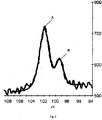
- Fig. 2 is an X-ray photoelectron spectroscopy (XPS) graph of the nano-composite nano-layer in accordance with an embodiment of the invention.
- XPS X-ray photoelectron spectroscopy
- Fig.2 shows two peaks: a high binding energy line (Peak A) at 101.66eV and a lower binding energy line (Peak B) at 99.40eV.
- Peak A is related to Si-N bonds that correspond to Si 3 N 4 .
- Peak B is more difficult to interpret.
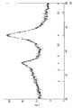
- Fig. 3 is an XRD spectrum of the nano-composite nano-layer obtained at a glazing angle in accordance with an embodiment of the invention.
- the lines numbered 1 are the peaks of cubic AlTiCrN.
- the lines numbered 2 are where peaks of crystalline Si 3 N 4 reference pattern 33-1160 appear.
- the only crystalline phase present in the nano-composite layer is a cubic phase and there is no hexagonal phase or trigonal phase or any crystalline Si 3 N 4 phase.
- the nano-composite nano-layer has a cubic (TiAlCr)N phase and an amorphous Si 3 N 4 phase.
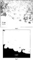
- Figs. 4 and 5 show photomicrographs taken of the nano-composite layer via transmission electron microscopy (TEM) with a 2 nm scale and via scanning transmission electron microscopy (STEM) with a 1 nm scale respectively.
- the TEM photomicrograph of Fig 4 shows a nano-composite structure of ordered crystalline grains and areas that are amorphous.
- STEM photomicrograph of Fig 5 shows a nano-composite structure of bright areas that have a greater atomic number than the dark areas.
- the bright areas correspond to the nc-(Ti x Al y Cr z )N grains and the dark areas surrounding the bright areas correspond to the lighter Si 3 N 4 matrix.
- the nano-crystalline grains are nc-(Ti x Al y Cr z )N (0.85 ⁇ x+y+z ⁇ 0.97) which are surrounded by an a-Si 3 N 4 matrix.
- the atomic ratio of titanium in nano-composite nano-layer is 0.25 ⁇ x ⁇ 0.75.
- the atomic ratio of chromium is 0.05 ⁇ z ⁇ 0.2 for increasing oxidation resistance and fracture toughness.
- the atomic ratio of aluminum in the nano-composite nano-layer is 0.25 ⁇ y ⁇ 0.72. It is known that a hexagonal phase of AlN will form when the sum of the atomic ratios of aluminum and silicon is over 0.75.
- the atomic ratio of silicon in the metallic elements of the nano-composite nano-layer is 0.03 ⁇ 1-x-y-z ⁇ 0.15 and 1-x-z ⁇ 0.75. Coatings comprising the nano-composite nano-layer have high temperature resistance and high hardness even at elevated temperatures.
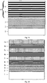
- Fig 1A shows a schematic illustration of an embodiment of the invention of a cutting tool with a substrate 1 coated with a multi-nano-layer 4.
- Nano-composite nano-layers 5 are alternated with crystalline nano-layers 6 to form a multi-nano-layer 4.
- the crystalline nano-layers 6 comprise a metallic or ceramic material.
- the metallic material is one or more metals selected from the group consisting of Ti, Zr, Hf, V, Nb, Ta, Cr, Mo, W, Al, Y and Ru.
- the ceramic material comprises a boride, a carbide, a nitride, an oxide, or any combination thereof, of one or more elements selected from the group consisting of Ti, Zr, Hf, V, Nb, Ta, Cr, Mo, W, Al, Si, Y and Ru.
- the ceramic material may be diamond or BN.
- the composition of the crystalline nano-layer is different from the composition of the nano-composite nano-layer. In some embodiments of the invention, there are two or more crystalline nano-layers 6 between sequential nano-composite nano-layers 5.
- crystalline nano-layers 6 that improve cohesiveness are of the formula (Ti a Al b Me 1-a-b )(C v N 1-v ) wherein Me is a metal selected from the group consisting of Cr, Mo, V, Nb, Ta, Zr, Hf, Y, and Ru wherein 0 ⁇ v ⁇ 1.
- Me is a metal selected from the group consisting of Cr, Mo, V, Nb, Ta, Zr, Hf, Y, and Ru wherein 0 ⁇ v ⁇ 1.
- the atomic ratio of titanium in the crystalline nano-layers 6 is 0 ⁇ a ⁇ 1.
- the atomic ratio of aluminum in the crystalline nano-layers 6 is 0 ⁇ b ⁇ 0.75.
- Both the nano-composite nano-layers and the crystalline nano-layers may have a thickness in the range of from about 1 nm to about 100 nm.
- the multi-nano-layer has from about 50 to about 300 nano-composite nano-layers.
- the multi-nano-layer effectively combines the advantages of the hard nano-composite nano-layer and the crystalline nano-layer.
- One benefit is that crack absorption is improved, leading to increased toughness of the coating.
- high hardness is not useful without toughness and both qualities are important in many applications for cutting tools.
- the multi-nano-layer according to the present invention may have crystalline nano-layers of one or more of the compositions defined above leading to varied characteristic properties of the coating as required by different applications.
- the thickness of the coating may be thicker than 3 ⁇ m without flaking. This is due to both the multi-nano-layer structure and to the presence of crystalline nano-layers having a lower compressive stress than the nano-composite nano-layers.
- Tool life is related to cutting speed, dimensions of the cut, tool angles, tool shape, coolant, chatter, etc.
- Cutting speed is the variable having by far the greatest influence on tool life.
- Higher heat resistance of the coating results in faster RPM without damaging the cutting tool.
- the coatings of the invention maintain the higher working temperature and oxidation resistance of known nano-composite coatings even though the multi-nano-layer of these coatings incorporate crystalline nano-layers that altogether amount to more or less half of the multi-nano-layer.
- the maximum working temperature for TiCN is about 550°C
- of TiAIN is about 800°C as compared with a maximum working temperature of the invention being about 1100°C.
- the intermediate layer 3 there is an intermediate layer 3 between the multi-nano-layer and the substrate 1 as shown in Fig 1A , which imparts toughness to the coating.
- the intermediate layer 3 is a ceramic layer that may be a boride, a nitride, a carbide, an oxide, or any combination thereof of one or more elements selected from the group consisting of Ti, Zr, Hf, V, Nb, Ta, Cr, Mo, W, Al, Si, Y and Ru.
- the intermediate layer 3 comprises (Ti a Al b Me 1-a-b )(C v N 1-v ) wherein Me is a metal selected from the group consisting of Cr, Mo, V, Nb, Ta, Zr, Hf, Y, and Ru wherein 0 ⁇ v ⁇ 1.
- Me is a metal selected from the group consisting of Cr, Mo, V, Nb, Ta, Zr, Hf, Y, and Ru wherein 0 ⁇ v ⁇ 1.
- the atomic ratio of titanium in the intermediate layer 3 is 0 ⁇ a ⁇ 1.
- the atomic ratio of aluminum in the intermediate layer 3 is 0 ⁇ b ⁇ 0.75.
- the intermediate layer 3 has a thickness of from about 0.5 ⁇ m to about 10 ⁇ m.
- adhesion layer 2 between the intermediate layer and the substrate, as shown in Fig 1A , which has a thickness of from about 0.1 ⁇ m to about 2 ⁇ m.
- the adhesion layer is of the formula (M w Al 1-w N (0.5 ⁇ w ⁇ 1) wherein M is titanium and/or chromium.
- Fig 1B shows a schematic illustration of another embodiment of the invention of a cutting tool with a substrate 1 coated with three multi-nano-layers 4i, 4ii, 4iii alternating with auxiliary layers 7i and 7ii.
- the auxiliary layer may be a metallic layer of one or metals sele cted from Ti, Zr, Hf, V, Nb, Ta, Cr, Mo, W, Al, Y and Ru.
- the auxiliary layer may be a boride, carbide, nitride, oxide, or any combination thereof of one or more elements selected from Ti, Zr, Hf, V, Nb, Ta, Cr, Mo, W, Al, Si, Y and Ru.
- the auxiliary layer may comprise diamond-like-carbon, diamond, or boron nitride.
- the outermost layer of the coating may be the multi-nano-layer, as shown in Fig. 1A , or the auxiliary layer 7iii, as shown in Fig IB.
- Auxiliary layers 7i, 7ii, 7iii etc. may all comprise a similar composition or, alternatively, one or more auxiliary layer may vary in composition.
- the coating may have either two multi-nano-layers or more than three multi-nano-layers. In some embodiments, there are two or more auxiliary layers between sequential multi-nano-layers. In some embodiments of the invention the intermediate layer comprises at least two intermediate sublayers 3i, 3ii differing in composition as shown in Fig IB.
- the cutting tools may optionally undergo a post coating thermal treatment in a protective atmosphere against oxidation such as nitrogen.
- the temperature of the thermal treatment is between 400°C and 1100°C preferably between 700°C and 900°C.
- the duration of the heat treatment is between 30 minutes and 180 minutes. This treatment further stabilizes and toughens the spinodal phase segregation of the nano-composite nano-layers.
- the substrate (1) of the cutting tool is of hard metal and the coating is deposited by a PVD method.
- Coating on cemented carbide was carried out in the following manner by using the known method of vacuum arc coating technology with round planar cathodes.
- the cathodes of the coating apparatus were provided with targets of TiAl, AlTi, and AlTiCrSi and with the substrates of milling inserts of cemented carbide, end mills of cemented carbide, and turning inserts of cemented carbide.
- the substrates were heated to a high deposition temperature of more than 500° C by a heater therein, and the vacuum chamber was fed with nitrogen gas. With the high pressure in the vacuum chamber kept at more than 4 Pa, arc discharging was started to form an adhesion layer of TiAlN (0.5 ⁇ m thick) on the surface of the substrate.
- the intermediate layer of AlTiN (2.5 ⁇ m thick) was then deposited onto the adhesion layer.
- the multi-nano-layer coating of alternating nano-layers of (1) nano-composite nano-layers and (2) crystalline nano-layers of TiAlN were then deposited by evaporating the targets of TiAl and AlTiCrSi respectively.
- a bias voltage of -30 V to -300 V was applied to the substrate so that the substrate remained at a minus potential with respect to the earth potential during the coating process.
- the nano-layers are all about 6 nm thick.
- the coated cutting tools the underwent a heat treatment at a temperature of more than 400 and up to 800 °C in a protective nitrogen atmosphere for at least 30 and up to 120 minutes.
- the cutting tools were then cooled gradually to room temperature in the protective nitrogen atmosphere.
- this coating will be referred to as Sample 1.
- the compositions of the layers of Sample 1 are in Table 1.
- Table 1 Layer Composition of coating film (atomic ratio) Structure Type* Coating thickness [ ⁇ m] Working temp.
- Comparative coatings were prepared on the same substrates and under the same conditions as described in Example 1.
- Comparative Sample 2 is a monolayer of TiAIN having a thickness of about 4 ⁇ m.
- Comparative Sample 3 is a layer of (Ti,Al,Si)N having a thickness of about 4 ⁇ m.
- Comparative Sample 4 is a nano-composite monolayer of a (Al,Ti,Cr,Si)N having a thickness of about 4.5 ⁇ m. Samples 2-4 were analyzed and the results are in Table 2.
- Table 2 Comparative Sample # Composition of coating film (atomic ratio) Structure Type* Coating thickness [ ⁇ m] Working temp.
Landscapes
- Chemical & Material Sciences (AREA)
- Chemical Kinetics & Catalysis (AREA)
- Engineering & Computer Science (AREA)
- Materials Engineering (AREA)
- Mechanical Engineering (AREA)
- Metallurgy (AREA)
- Organic Chemistry (AREA)
- Inorganic Chemistry (AREA)
- Cutting Tools, Boring Holders, And Turrets (AREA)
- Drilling Tools (AREA)
- Laminated Bodies (AREA)
- Physical Vapour Deposition (AREA)
Claims (15)
- Beschichtetes Schneidwerkzeug, das ein Substrat (1) und eine Beschichtung aufweist; wobei:die Beschichtung mindestens eine Mehrfach-Nanoschicht (4) aufweist, die Mehrfach-Nanoschicht (4) eine Vielzahl von Nanoverbund-Nanoschichten (5) und zweite Nanoschichten (6) aufweist;die Nanoverbund-Nanoschichten (5) aus nanokristallinem kubischen (TixAlyCrz)N bestehen, das in eine amorphe Si3N4-Matrix eingebettet ist, wobei x=0,42, y=0,42, z=0,1, und 1-x-y-z=0,06;das Atomverhältnis von Silizium in den Metallelementen 1-x-y-z beträgt; undeine Dicke der Nanoverbund-Nanoschichten (5) von 1 nm bis 100 nm beträgt und die zweite Nanoschicht (6) kristallin ist und aufweist:(a) ein Metallmaterial, das aus einem oder mehreren Metallen besteht, die aus der Gruppe ausgewählt sind, die aus Ti, Zr, Hf, V, Nb, Ta, Cr, Mo, W, Al, Y und Ru besteht; oder(b) ein Keramikmaterial, das aufweist:(b1) eines oder mehreres von einem Borid, Karbid, Nitrid oder Oxid von einem oder mehreren Elementen, die aus der Gruppe ausgewählt sind, die aus Ti, Zr, Hf, V, Nb, Ta, Cr, Mo, W, Al, Si, Y und Ru besteht,(b2) Diamant, oder(b3) BN,wobei eine Dicke der zweiten Nanoschicht (6) von 1 nm bis 100 nm beträgt;wobei die Mehrfach-Nanoschicht Nanoverbund-Nanoschichten aufweist, die abwechselnd mit zweiten Nanoschichten aufeinandergeschichtet sind;das Substrat (1) aus der Gruppe ausgewählt ist, die aus Schnelldrehstahl, Hartmetallen, Oxidkeramiken, Karbidkeramiken, Boridkeramiken, Superschleifmatrialien, PcBN, PCD und Keramik-Metall-Verbundwerkstoffen und Kombinationen davon besteht.
- Beschichtetes Schneidwerkzeug nach Anspruch 1, wobei die Mehrfach-Nanoschicht mindestens zwei Nanoverbund-Nanoschichten mit unterschiedlichen Zusammensetzungen aufweist.
- Beschichtetes Schneidwerkzeug nach Anspruch 1, wobei die Mehrfach-Nanoschicht eine Dicke von mindestens 3 µm aufweist.
- Beschichtetes Schneidwerkzeug nach Anspruch 3, wobei:die zweite Nanoschicht (TiaAlbMe1-a-b)(CvN1-v) aufweist, wobei 0≤a≤1, 0≤b<0,75, und 0≤v≤1; undMe ein Metall ist, das aus der Gruppe ausgewählt ist, die aus Cr, Mo, V, Nb, Ta, Zr, Hf, Y und Ru besteht.
- Beschichtetes Schneidwerkzeug nach Anspruch 3, wobei die Mehrfach-Nanoschicht mindestens zwei zweite Nanoschichten mit unterschiedlichen Zusammensetzungen aufweist, oder
wobei die Mehrfach-Nanoschicht zwei oder mehrere zweite Nanoschichten zwischen aufeinanderfolgenden Nanoverbund-Nanoschichten aufweist, oder
wobei die Mehrfach-Nanoschicht 50 bis 300 Nanoverbund-Nanoschichten aufweist. - Beschichtetes Schneidwerkzeug nach Anspruch 1, wobei:die Beschichtung ferner mindestens eine Zwischenschicht zwischen dem Substrat undder Mehrfach-Nanoschicht aufweist; unddie Zwischenschicht eines oder mehrere von einem Borid, Karbid, Nitrid oder Oxid von einem oder mehreren Elementen aufweist, die aus der Gruppe ausgewählt sind, die aus Ti, Zr, Hf, V, Nb, Ta, Cr, Mo, W, Al, Si, Y und Ru besteht.
- Beschichtetes Schneidwerkzeug nach Anspruch 6, wobei:die mindestens eine Zwischenschicht aus (TiaAlbMe1-a-b)(CvN1-v) besteht, wobei 0≤a≤1, 0≤b<0,75, und 0≤v≤1;Me ein Metall ist, das aus der Gruppe ausgewählt ist, die aus Cr, Mo, V, Nb, Ta, Zr, Hf, Y und Ru besteht; undeine Dicke der Zwischenschicht von 0,5 µm bis 10 µm beträgt, oder wobei:die Zwischenschicht ferner mindestens zwei Teilschichten mit unterschiedlicher Zusammensetzung aufweist; undeine Dicke der Teilschichten von 1 nm bis 500 nm beträgt.
- Beschichtetes Schneidwerkzeug nach Anspruch 6, wobei:die Beschichtung ferner eine Haftschicht zwischen dem Substrat und der Zwischenschicht aufweist, wobei sich eine Zusammensetzung der Haftschicht von einer Zusammensetzung der Zwischenschicht unterscheidet;die Haftschicht mindestens eine Schicht aus (MewAl1-w)N aufweist, wobei 0,5≤w≤1;M Titan und/oder Chrom ist; undeine Dicke der Haftschicht von 0,1 µm bis 2 µm beträgt.
- Beschichtetes Schneidwerkzeug nach Anspruch 1, wobei die Beschichtung aufweist:mehr als eine Mehrfach-Nanoschicht und mindestens eine Hilfsschicht zwischen den Mehrfach-Nanoschichten, wobei die mindestens eine Hilfsschicht aufweist:(a) ein Metallmaterial, das aus einem oder mehreren Metallen besteht, die aus der Gruppe ausgewählt sind, die aus Ti, Zr, Hf, V, Nb, Ta, Cr, Mo, W, Al, Y und Ru besteht; oder(b) ein Keramikmaterial, das aus der Gruppe ausgewählt ist, die besteht aus:(b1) einem oder mehreren von einem Borid, Karbid, Nitrid oder Oxid von einem oder mehreren Elementen, die aus der Gruppe ausgewählt sind, die aus Ti, Zr, Hf, V, Nb, Ta, Cr, Mo, W, Al, Si, Y und Ru besteht,(b2) Diamant,(b3) diamantartigen Kohlenstoff, und(b4) BN.
- Beschichtetes Schneidwerkzeug nach Anspruch 1, das ferner eine oberste Schicht aufweist, wobei die oberste Schicht die äußerste Schicht der Beschichtung ist und aufweist:(a) ein Metallmaterial aus einem oder mehreren Metallen, die aus der Gruppe ausgewählt sind, die aus Ti, Zr, Hf, V, Nb, Ta, Cr, Mo, W, Al, Y und Ru besteht; oder(b) ein Keramikmaterial, das aus der Gruppe ausgewählt ist, die besteht aus:(b1) einem oder mehreren von einem Borid, Karbid, Nitrid oder Oxid von einem oder mehreren Elementen, die aus der Gruppe ausgewählt sind, die aus Ti, Zr, Hf, V, Nb, Ta, Cr, Mo, W, Al, Si, Y und Ru besteht,(b2) Diamant,(b3) diamantartigen Kohlenstoff, und(b4) BN.
- Verfahren zum Beschichten eines Schneidwerkzeugsubstrats mit einer Beschichtung, die mindestens eine Mehrfach-Nanoschicht aufweist, wobei das Verfahren die Schritte aufweist:a) Abscheiden einer Nanoverbund-Nanoschicht über dem Substrat, wobei die Nanoverbund-Nanoschicht aus nanokristallinem kubischen (TixAlyCrz)N besteht, das in eine amorphe Si3N4-Matrix eingebettet ist, wobei x=0,42, y=0,42, z=0,1, und 1-x-y-z=0,06, wobei:das Atomverhältnis von Silizium in den Metallelementen 1-x-y-z ist; undeine Dicke der Nanoverbund-Nanoschicht von 1 nm bis 100 nm beträgt;b) Abscheiden von mindestens einer zweiten Nanoschicht über der Nanoverbund-Nanoschicht, wobei die zweite Nanoschicht kristallin ist, eine Dicke von 1 nm bis 100 nm aufweist und aufweist:(b1) ein Metallmaterial, das aus einem oder mehreren Metallen besteht, die aus der Gruppe ausgewählt sind, die aus Ti, Zr, Hf, V, Nb, Ta, Cr, Mo, W, Al, Y und Ru besteht; oder(b2) ein Keramikmaterial, das aufweist:(b21) eines oder mehreres von einem Borid, Karbid, Nitrid oder Oxid von einem oder mehreren Elementen, die aus der Gruppe ausgewählt sind, die aus Ti, Zr, Hf, V, Nb, Ta, Cr, Mo, W, Al, Si, Y und Ru besteht,(b22) Diamant, oder(b23) BN; undc) abwechselndes Ausführen das Schritts a und des Schritts b 50 bis 300 Mal, wobei das Substrat aus der Gruppe ausgewählt ist, die aus Schnelldrehstahl, Hartmetallen, Oxidkeramiken, Karbidkeramiken, Boridkeramiken, Superschleifmatrialien, PcBN, PCD und Keramik-Metall-Verbundwerkstoffen und Kombinationen davon besteht, wobei die Beschichtung bei einer Abscheidungstemperatur zwischen 500°C und 600°C abgeschieden wird.
- Verfahren nach Anspruch 11, wobei die Beschichtung mit einer PVD-Technik unter einem Stickstoffpartialdruck von mindestens 0,02 mbar abgeschieden wird.
- Verfahren nach Anspruch 11, das ferner einen oder mehrere Schritte aufweist:i) Abscheiden einer Haftschicht über dem Substrat vor dem Durchführen des Schritts a), wobei: die Haftschicht mindestens eine Schicht aus (MewAl1-w)N aufweist, wobei 0,5≤w≤1;
M Titan und/oder Chrom ist; und
eine Dicke der Haftschicht von 0,1 µm bis 2 µm beträgt; undii) Abscheiden von mindestens einer Zwischenschicht über der Haftschicht, wobei die Zwischenschicht eines oder mehrere von einem Borid, Karbid, Nitrid oder Oxid von einem oder mehreren Elementen aufweist, die aus der Gruppe ausgewählt sind, die aus Ti, Zr, Hf, V, Nb, Ta, Cr, Mo, W, Al, Si, Y und Ru besteht, wobei, vorzugsweise:eine Dicke der Zwischenschicht 0,5 µm bis 10 µm beträgt.die mindestens eine Zwischenschicht (TiaAlbMe1-a-b)(CvN1-v) aufweist, wobei 0≤a≤1, 0≤b<0,75, und 0≤v≤1;Me ein Metall ist, das aus der Gruppe ausgewählt ist, die aus Cr, Mo, V, Nb, Ta, Zr, Hf, Y und Ru besteht; und - Verfahren nach Anspruch 11, das ferner den Schritt aufweist:d) Behandeln des beschichteten Schneidwerkzeugs in einer Schutzatmosphäre aus Stickstoff bei einer Temperatur von 400°C bis 1100°C für eine Dauer von 20 Minuten bis 180 Minuten.
- Verfahren nach Anspruch 11, wobei die Beschichtung mehr als eine Mehrfach-Nanoschicht aufweist und das Verfahren ferner aufweist:e) Abscheiden mindestens einer Hilfsschicht über der Mehrfach-Nanoschicht, wobei die mindestens eine Hilfsschicht aufweist:(e1) ein Metallmaterial, das aus einem oder mehreren Metallen besteht, die aus der Gruppe ausgewählt sind, die aus Ti, Zr, Hf, V, Nb, Ta, Cr, Mo, W, Al, Y und Ru besteht; oder(e2) ein Keramikmaterial, das aus der Gruppe ausgewählt ist, die besteht aus:(e21) eines oder mehrere von einem Borid, Karbid, Nitrid oder Oxid von einem oder mehreren Elementen, die aus der Gruppe ausgewählt sind, die aus Ti, Zr, Hf, V, Nb, Ta, Cr, Mo, W, Al, Si, Y und Ru besteht,(e22) Diamant,(e23) diamantartigen Kohlenstoff, und(e24) BN;f) Durchführen der Schritte a-c; undg) abwechselndes Ausführen des Schritt e und des Schritts f mindestens einmal.
Priority Applications (1)
| Application Number | Priority Date | Filing Date | Title |
|---|---|---|---|
| PL10807674T PL2524066T3 (pl) | 2010-01-11 | 2010-12-14 | Powleczone narzędzie tnące |
Applications Claiming Priority (2)
| Application Number | Priority Date | Filing Date | Title |
|---|---|---|---|
| IL20324210 | 2010-01-11 | ||
| PCT/IL2010/001054 WO2011083457A1 (en) | 2010-01-11 | 2010-12-14 | Coated cutting tool |
Publications (2)
| Publication Number | Publication Date |
|---|---|
| EP2524066A1 EP2524066A1 (de) | 2012-11-21 |
| EP2524066B1 true EP2524066B1 (de) | 2018-11-21 |
Family
ID=43799491
Family Applications (1)
| Application Number | Title | Priority Date | Filing Date |
|---|---|---|---|
| EP10807674.6A Active EP2524066B1 (de) | 2010-01-11 | 2010-12-14 | Beschichtetes schneidwerkzeug |
Country Status (12)
| Country | Link |
|---|---|
| US (1) | US8545997B2 (de) |
| EP (1) | EP2524066B1 (de) |
| JP (1) | JP5896918B2 (de) |
| KR (1) | KR101751562B1 (de) |
| CN (1) | CN102812149B (de) |
| BR (1) | BR112012016898A2 (de) |
| ES (1) | ES2699177T3 (de) |
| PL (1) | PL2524066T3 (de) |
| PT (1) | PT2524066T (de) |
| RU (1) | RU2542185C2 (de) |
| TR (1) | TR201819344T4 (de) |
| WO (1) | WO2011083457A1 (de) |
Families Citing this family (36)
| Publication number | Priority date | Publication date | Assignee | Title |
|---|---|---|---|---|
| DE102010039035A1 (de) * | 2010-08-06 | 2012-02-09 | Walter Ag | Schneidwerkzeug mit mehrlagiger Beschichtung |
| EP2495081B1 (de) * | 2011-03-01 | 2014-05-07 | GFD Gesellschaft für Diamantprodukte mbH | Schneidewerkzeug mit Klinge aus feinkristallinem Diamant |
| WO2013045039A2 (en) * | 2011-09-30 | 2013-04-04 | Oerlikon Trading Ag, Trübbach | Aluminum titanium nitride coating with adapted morphology for enhanced wear resistance in machining operations and method thereof |
| KR101684412B1 (ko) * | 2012-08-10 | 2016-12-08 | 가부시키가이샤 탕가로이 | 피복 공구 |
| US10316592B2 (en) * | 2012-09-11 | 2019-06-11 | Halliburton Energy Services, Inc. | Cutter for use in well tools |
| JP6015922B2 (ja) * | 2012-10-16 | 2016-10-26 | 三菱マテリアル株式会社 | 表面被覆切削工具 |
| CN103143761B (zh) * | 2013-03-22 | 2015-06-24 | 武汉大学 | 一种AlTiN-MoN纳米多层复合涂层铣刀及其制备方法 |
| DE102013011071A1 (de) * | 2013-07-03 | 2015-01-08 | Oerlikon Trading Ag, Trübbach | TixSi1-xN Schichten mit CryAl1-yN Haftschicht und ihre Herstellung |
| DE102013011073A1 (de) * | 2013-07-03 | 2015-01-08 | Oerlikon Trading Ag, Trübbach | TlxSi1-xN Schichten und ihre Herstellung |
| KR102178189B1 (ko) | 2013-07-03 | 2020-11-13 | 외를리콘 서피스 솔루션즈 아게, 페피콘 | TixSi1-xN 층 및 그의 생산 |
| JP6102653B2 (ja) * | 2013-09-19 | 2017-03-29 | 三菱マテリアル株式会社 | 表面被覆切削工具 |
| CN103757597B (zh) * | 2014-02-07 | 2016-03-23 | 上海理工大学 | 一种TiN/CrAlSiN纳米复合多层涂层及其制备方法 |
| US9321117B2 (en) | 2014-03-18 | 2016-04-26 | Vermeer Manufacturing Company | Automatic system for abrasive hardfacing |
| CN107107206B (zh) * | 2014-10-29 | 2020-07-28 | 住友电气工业株式会社 | 复合金刚石体和复合金刚石工具 |
| CN104789933B (zh) * | 2015-04-28 | 2017-06-20 | 重庆文理学院 | 一种纳米复合涂层及其沉积方法 |
| CN104928637B (zh) * | 2015-05-19 | 2017-12-22 | 上海新弧源涂层技术有限公司 | 高硬度CrAlSiN纳米复合结构保护性涂层及其制备方法 |
| JP6789986B2 (ja) * | 2015-05-21 | 2020-11-25 | ヴァルター アーゲー | 多層アークpvdコーティングを有する工具 |
| US10675690B2 (en) | 2015-09-04 | 2020-06-09 | Osg Corporation | Hard coating and hard coating-covered member |
| JP6577037B2 (ja) * | 2015-09-04 | 2019-09-18 | オーエスジー株式会社 | 硬質被膜および硬質被膜被覆部材 |
| RU2620521C2 (ru) * | 2015-10-06 | 2017-05-26 | Федеральное государственное автономное образовательное учреждение высшего профессионального образования "Белгородский государственный национальный исследовательский университет" (НИУ "БелГУ") | Износостойкое покрытие для режущего инструмента |
| US11224920B2 (en) * | 2015-12-22 | 2022-01-18 | Kyocera Corporation | Coated tool |
| US10246335B2 (en) * | 2016-05-27 | 2019-04-02 | Baker Hughes, A Ge Company, Llc | Methods of modifying surfaces of diamond particles, and related diamond particles and earth-boring tools |
| CN105862002B (zh) * | 2016-06-07 | 2018-11-30 | 中国科学院兰州化学物理研究所 | 类牡蛎壳的仿生多层强韧化薄膜 |
| CN107513690B (zh) * | 2016-06-17 | 2019-07-02 | 中国科学院深圳先进技术研究院 | 一种类金刚石/立方氮化硼多层复合涂层及其制备方法 |
| KR102144241B1 (ko) * | 2016-10-25 | 2020-08-12 | 오에스지 가부시키가이샤 | 경질 피막 및 경질 피막 피복 부재 |
| WO2018162558A1 (en) * | 2017-03-09 | 2018-09-13 | Sandvik Intellectual Property Ab | A coated cutting tool |
| CN107747092B (zh) * | 2017-10-10 | 2019-08-23 | 岭南师范学院 | 一种耐高温硬质复合涂层及其制备方法和涂层刀具 |
| CN107937914B (zh) * | 2017-11-27 | 2019-12-24 | 浙江工业大学 | 一种在不锈钢表面的过渡层上制备金刚石薄膜的方法 |
| CN108118299B (zh) * | 2017-12-20 | 2019-06-28 | 中国科学院合肥物质科学研究院 | 一种氮化钼基梯度多元纳米复合涂层及制备方法 |
| WO2019239654A1 (ja) * | 2018-06-15 | 2019-12-19 | 住友電工ハードメタル株式会社 | 表面被覆切削工具、及びその製造方法 |
| EP3877565A1 (de) * | 2018-11-08 | 2021-09-15 | Oerlikon Surface Solutions AG, Pfäffikon | Korrosionsbeständige beschichtungen |
| MX2022000148A (es) * | 2019-07-11 | 2022-02-17 | Knight Acquisition B V | Hoja de sierra u otra herramienta de corte comprendiendo un recubrimiento. |
| CN110578122A (zh) * | 2019-10-18 | 2019-12-17 | 天津职业技术师范大学(中国职业培训指导教师进修中心) | 一种AlTiN/AlTiSiN多层纳米复合涂层的制备工艺 |
| CN111112657A (zh) * | 2019-12-30 | 2020-05-08 | 无锡市星火金刚石工具有限公司 | 一种pcd刀具复合片 |
| CN111304618B (zh) * | 2020-04-14 | 2021-12-21 | 上海工具厂有限公司 | 一种纳米复合涂层及其制备方法 |
| CN115505882A (zh) * | 2022-09-14 | 2022-12-23 | 广东工业大学 | 氮化物结合氧化物双涂层的制备方法及涂层刀具 |
Family Cites Families (18)
| Publication number | Priority date | Publication date | Assignee | Title |
|---|---|---|---|---|
| JPH08206902A (ja) * | 1994-12-01 | 1996-08-13 | Sumitomo Electric Ind Ltd | 切削用焼結体チップおよびその製造方法 |
| EP1698714B1 (de) * | 2000-12-28 | 2009-09-02 | Kabushiki Kaisha Kobe Seiko Sho | Target zur Bildung einer Hartschicht |
| JP4112834B2 (ja) * | 2000-12-28 | 2008-07-02 | 株式会社神戸製鋼所 | 切削工具用硬質皮膜を形成するためのターゲット |
| JP3586216B2 (ja) | 2001-05-11 | 2004-11-10 | 日立ツール株式会社 | 硬質皮膜被覆工具 |
| JP3991272B2 (ja) * | 2003-01-20 | 2007-10-17 | 三菱マテリアル神戸ツールズ株式会社 | 高速重切削条件で硬質被覆層がすぐれた耐摩耗性を発揮する表面被覆超硬合金製切削工具 |
| JP4707541B2 (ja) * | 2005-03-24 | 2011-06-22 | 日立ツール株式会社 | 硬質皮膜被覆部材 |
| US7537822B2 (en) | 2005-05-26 | 2009-05-26 | Hitachi Tool Engineering, Ltd. | Hard-coated member |
| JP4950499B2 (ja) | 2006-02-03 | 2012-06-13 | 株式会社神戸製鋼所 | 硬質皮膜およびその成膜方法 |
| RU74128U1 (ru) * | 2006-12-25 | 2008-06-20 | Закрытое акционерное общество Инновационные технологии получения наноматериалов и нанесения покрытий-"ИНАКОТЕК" | Многокомпонентное наноструктурированное пленочное покрытие |
| SE0602814L (sv) * | 2006-12-27 | 2008-06-28 | Sandvik Intellectual Property | Skärverktyg med multiskiktbeläggning |
| JP2008240079A (ja) * | 2007-03-28 | 2008-10-09 | Tungaloy Corp | 被覆部材 |
| SE0701320L (sv) * | 2007-06-01 | 2008-12-02 | Sandvik Intellectual Property | Belagd hårdmetall för formverktygsapplikationer |
| AT506133B1 (de) * | 2007-11-16 | 2009-11-15 | Boehlerit Gmbh & Co Kg | Reibrührschweisswerkzeug |
| CN101407905B (zh) | 2008-07-28 | 2010-06-23 | 株洲钻石切削刀具股份有限公司 | 一种多组元涂层的硬质合金切削刀具 |
| RU2371513C1 (ru) * | 2008-09-17 | 2009-10-27 | Федеральное государственное учреждение Российский научный центр "Курчатовский институт" | Способ получения наноструктурированных пленочных покрытий (варианты) |
| JP2010168638A (ja) * | 2009-01-26 | 2010-08-05 | Kobe Steel Ltd | 硬質皮膜被覆部材および成形用治工具 |
| JP5043908B2 (ja) * | 2009-09-04 | 2012-10-10 | 株式会社神戸製鋼所 | 微細結晶硬質皮膜の形成方法 |
| CN101879794B (zh) * | 2010-05-31 | 2012-10-17 | 武汉嘉树科技有限公司 | CrTiAlSiN纳米复合涂层、沉积有该涂层的刀具及其制备方法 |
-
2010
- 2010-12-14 EP EP10807674.6A patent/EP2524066B1/de active Active
- 2010-12-14 PL PL10807674T patent/PL2524066T3/pl unknown
- 2010-12-14 PT PT10807674T patent/PT2524066T/pt unknown
- 2010-12-14 JP JP2012547584A patent/JP5896918B2/ja active Active
- 2010-12-14 WO PCT/IL2010/001054 patent/WO2011083457A1/en active Application Filing
- 2010-12-14 BR BR112012016898A patent/BR112012016898A2/pt not_active IP Right Cessation
- 2010-12-14 TR TR2018/19344T patent/TR201819344T4/tr unknown
- 2010-12-14 RU RU2012134434/02A patent/RU2542185C2/ru active
- 2010-12-14 CN CN201080061150.3A patent/CN102812149B/zh active Active
- 2010-12-14 KR KR1020127017939A patent/KR101751562B1/ko active IP Right Grant
- 2010-12-14 ES ES10807674T patent/ES2699177T3/es active Active
-
2011
- 2011-01-03 US US12/983,689 patent/US8545997B2/en active Active
Non-Patent Citations (1)
| Title |
|---|
| None * |
Also Published As
| Publication number | Publication date |
|---|---|
| BR112012016898A2 (pt) | 2018-06-05 |
| EP2524066A1 (de) | 2012-11-21 |
| JP2013516331A (ja) | 2013-05-13 |
| CN102812149A (zh) | 2012-12-05 |
| PL2524066T3 (pl) | 2019-02-28 |
| RU2012134434A (ru) | 2014-02-20 |
| KR20120123311A (ko) | 2012-11-08 |
| WO2011083457A1 (en) | 2011-07-14 |
| US20110171444A1 (en) | 2011-07-14 |
| TR201819344T4 (tr) | 2019-01-21 |
| PT2524066T (pt) | 2018-12-24 |
| JP5896918B2 (ja) | 2016-03-30 |
| CN102812149B (zh) | 2014-08-27 |
| US8545997B2 (en) | 2013-10-01 |
| RU2542185C2 (ru) | 2015-02-20 |
| KR101751562B1 (ko) | 2017-06-27 |
| ES2699177T3 (es) | 2019-02-07 |
Similar Documents
| Publication | Publication Date | Title |
|---|---|---|
| EP2524066B1 (de) | Beschichtetes schneidwerkzeug | |
| KR101432847B1 (ko) | 하드 코팅을 가지는 작업편 | |
| EP1722009B1 (de) | Dünne verschleissfeste Beschichtung | |
| EP1400609B1 (de) | Ausscheidungsgehärtete Verschleissschutzschicht | |
| EP2438209B1 (de) | Nanolaminiertes und beschichtetes schneidewerkzeug | |
| EP1877595B1 (de) | Mit abriebfester schicht beschichteter schneidwerkzeugeinsatz, vollschaftfräser oder bohrer | |
| US9540722B2 (en) | Body with a metal based nitride layer and a method for coating the body | |
| EP2269752B1 (de) | Oberflächenbeschichtetes schneidewerkzeug | |
| EP2643498B1 (de) | Beschichteter schneideeinsatz für metallbearbeitung, der hohe temperaturen bewirkt | |
| EP1347076B1 (de) | PVD-beschichteter Werkzeugschneideinsatz | |
| EP2636764B1 (de) | Nanolaminiertes und beschichtetes Schneidewerkzeug | |
| EP2100681B1 (de) | Oberflächenbeschichtetes werkzeug und verfahren zur schneidbearbeitung eines objekts | |
| EP1452621A2 (de) | Verschleissfeste Komposit-Oberflächenbeschichtung | |
| JP5909273B2 (ja) | 硬質皮膜および硬質皮膜の製造方法 | |
| CZ2006400A3 (cs) | Vícevrstvý povlak pro konečnou úpravu kalených ocelí | |
| IL209811A (en) | Hard coating and method of forming | |
| KR101079902B1 (ko) | 표면 피복 절삭 공구 | |
| Varela et al. | NbC-Ni coatings deposited by DC reactive magnetron sputtering: Effect of Ni content on mechanical properties, thermal stability and oxidation resistance | |
| EP3786313B1 (de) | Beschichtetes schneidwerkzeug |
Legal Events
| Date | Code | Title | Description |
|---|---|---|---|
| PUAI | Public reference made under article 153(3) epc to a published international application that has entered the european phase |
Free format text: ORIGINAL CODE: 0009012 |
|
| 17P | Request for examination filed |
Effective date: 20120809 |
|
| AK | Designated contracting states |
Kind code of ref document: A1 Designated state(s): AL AT BE BG CH CY CZ DE DK EE ES FI FR GB GR HR HU IE IS IT LI LT LU LV MC MK MT NL NO PL PT RO RS SE SI SK SM TR |
|
| DAX | Request for extension of the european patent (deleted) | ||
| 17Q | First examination report despatched |
Effective date: 20171102 |
|
| GRAP | Despatch of communication of intention to grant a patent |
Free format text: ORIGINAL CODE: EPIDOSNIGR1 |
|
| INTG | Intention to grant announced |
Effective date: 20180529 |
|
| GRAS | Grant fee paid |
Free format text: ORIGINAL CODE: EPIDOSNIGR3 |
|
| GRAA | (expected) grant |
Free format text: ORIGINAL CODE: 0009210 |
|
| AK | Designated contracting states |
Kind code of ref document: B1 Designated state(s): AL AT BE BG CH CY CZ DE DK EE ES FI FR GB GR HR HU IE IS IT LI LT LU LV MC MK MT NL NO PL PT RO RS SE SI SK SM TR |
|
| REG | Reference to a national code |
Ref country code: CH Ref legal event code: EP |
|
| REG | Reference to a national code |
Ref country code: IE Ref legal event code: FG4D |
|
| REG | Reference to a national code |
Ref country code: DE Ref legal event code: R096 Ref document number: 602010055335 Country of ref document: DE |
|
| REG | Reference to a national code |
Ref country code: AT Ref legal event code: REF Ref document number: 1067608 Country of ref document: AT Kind code of ref document: T Effective date: 20181215 |
|
| REG | Reference to a national code |
Ref country code: PT Ref legal event code: SC4A Ref document number: 2524066 Country of ref document: PT Date of ref document: 20181224 Kind code of ref document: T Free format text: AVAILABILITY OF NATIONAL TRANSLATION Effective date: 20181214 |
|
| REG | Reference to a national code |
Ref country code: SE Ref legal event code: TRGR |
|
| REG | Reference to a national code |
Ref country code: ES Ref legal event code: FG2A Ref document number: 2699177 Country of ref document: ES Kind code of ref document: T3 Effective date: 20190207 |
|
| REG | Reference to a national code |
Ref country code: NL Ref legal event code: MP Effective date: 20181121 |
|
| PG25 | Lapsed in a contracting state [announced via postgrant information from national office to epo] |
Ref country code: BG Free format text: LAPSE BECAUSE OF FAILURE TO SUBMIT A TRANSLATION OF THE DESCRIPTION OR TO PAY THE FEE WITHIN THE PRESCRIBED TIME-LIMIT Effective date: 20190221 Ref country code: NO Free format text: LAPSE BECAUSE OF FAILURE TO SUBMIT A TRANSLATION OF THE DESCRIPTION OR TO PAY THE FEE WITHIN THE PRESCRIBED TIME-LIMIT Effective date: 20190221 Ref country code: FI Free format text: LAPSE BECAUSE OF FAILURE TO SUBMIT A TRANSLATION OF THE DESCRIPTION OR TO PAY THE FEE WITHIN THE PRESCRIBED TIME-LIMIT Effective date: 20181121 Ref country code: IS Free format text: LAPSE BECAUSE OF FAILURE TO SUBMIT A TRANSLATION OF THE DESCRIPTION OR TO PAY THE FEE WITHIN THE PRESCRIBED TIME-LIMIT Effective date: 20190321 Ref country code: LT Free format text: LAPSE BECAUSE OF FAILURE TO SUBMIT A TRANSLATION OF THE DESCRIPTION OR TO PAY THE FEE WITHIN THE PRESCRIBED TIME-LIMIT Effective date: 20181121 Ref country code: LV Free format text: LAPSE BECAUSE OF FAILURE TO SUBMIT A TRANSLATION OF THE DESCRIPTION OR TO PAY THE FEE WITHIN THE PRESCRIBED TIME-LIMIT Effective date: 20181121 Ref country code: HR Free format text: LAPSE BECAUSE OF FAILURE TO SUBMIT A TRANSLATION OF THE DESCRIPTION OR TO PAY THE FEE WITHIN THE PRESCRIBED TIME-LIMIT Effective date: 20181121 |
|
| PG25 | Lapsed in a contracting state [announced via postgrant information from national office to epo] |
Ref country code: AL Free format text: LAPSE BECAUSE OF FAILURE TO SUBMIT A TRANSLATION OF THE DESCRIPTION OR TO PAY THE FEE WITHIN THE PRESCRIBED TIME-LIMIT Effective date: 20181121 Ref country code: RS Free format text: LAPSE BECAUSE OF FAILURE TO SUBMIT A TRANSLATION OF THE DESCRIPTION OR TO PAY THE FEE WITHIN THE PRESCRIBED TIME-LIMIT Effective date: 20181121 Ref country code: NL Free format text: LAPSE BECAUSE OF FAILURE TO SUBMIT A TRANSLATION OF THE DESCRIPTION OR TO PAY THE FEE WITHIN THE PRESCRIBED TIME-LIMIT Effective date: 20181121 Ref country code: GR Free format text: LAPSE BECAUSE OF FAILURE TO SUBMIT A TRANSLATION OF THE DESCRIPTION OR TO PAY THE FEE WITHIN THE PRESCRIBED TIME-LIMIT Effective date: 20190222 |
|
| PG25 | Lapsed in a contracting state [announced via postgrant information from national office to epo] |
Ref country code: DK Free format text: LAPSE BECAUSE OF FAILURE TO SUBMIT A TRANSLATION OF THE DESCRIPTION OR TO PAY THE FEE WITHIN THE PRESCRIBED TIME-LIMIT Effective date: 20181121 |
|
| REG | Reference to a national code |
Ref country code: CH Ref legal event code: PL |
|
| REG | Reference to a national code |
Ref country code: DE Ref legal event code: R097 Ref document number: 602010055335 Country of ref document: DE |
|
| PG25 | Lapsed in a contracting state [announced via postgrant information from national office to epo] |
Ref country code: MC Free format text: LAPSE BECAUSE OF FAILURE TO SUBMIT A TRANSLATION OF THE DESCRIPTION OR TO PAY THE FEE WITHIN THE PRESCRIBED TIME-LIMIT Effective date: 20181121 Ref country code: RO Free format text: LAPSE BECAUSE OF FAILURE TO SUBMIT A TRANSLATION OF THE DESCRIPTION OR TO PAY THE FEE WITHIN THE PRESCRIBED TIME-LIMIT Effective date: 20181121 Ref country code: SM Free format text: LAPSE BECAUSE OF FAILURE TO SUBMIT A TRANSLATION OF THE DESCRIPTION OR TO PAY THE FEE WITHIN THE PRESCRIBED TIME-LIMIT Effective date: 20181121 Ref country code: EE Free format text: LAPSE BECAUSE OF FAILURE TO SUBMIT A TRANSLATION OF THE DESCRIPTION OR TO PAY THE FEE WITHIN THE PRESCRIBED TIME-LIMIT Effective date: 20181121 Ref country code: SK Free format text: LAPSE BECAUSE OF FAILURE TO SUBMIT A TRANSLATION OF THE DESCRIPTION OR TO PAY THE FEE WITHIN THE PRESCRIBED TIME-LIMIT Effective date: 20181121 Ref country code: LU Free format text: LAPSE BECAUSE OF NON-PAYMENT OF DUE FEES Effective date: 20181214 |
|
| REG | Reference to a national code |
Ref country code: IE Ref legal event code: MM4A |
|
| PLBE | No opposition filed within time limit |
Free format text: ORIGINAL CODE: 0009261 |
|
| STAA | Information on the status of an ep patent application or granted ep patent |
Free format text: STATUS: NO OPPOSITION FILED WITHIN TIME LIMIT |
|
| REG | Reference to a national code |
Ref country code: BE Ref legal event code: MM Effective date: 20181231 |
|
| 26N | No opposition filed |
Effective date: 20190822 |
|
| PG25 | Lapsed in a contracting state [announced via postgrant information from national office to epo] |
Ref country code: IE Free format text: LAPSE BECAUSE OF NON-PAYMENT OF DUE FEES Effective date: 20181214 Ref country code: SI Free format text: LAPSE BECAUSE OF FAILURE TO SUBMIT A TRANSLATION OF THE DESCRIPTION OR TO PAY THE FEE WITHIN THE PRESCRIBED TIME-LIMIT Effective date: 20181121 |
|
| PG25 | Lapsed in a contracting state [announced via postgrant information from national office to epo] |
Ref country code: BE Free format text: LAPSE BECAUSE OF NON-PAYMENT OF DUE FEES Effective date: 20181231 |
|
| PG25 | Lapsed in a contracting state [announced via postgrant information from national office to epo] |
Ref country code: CH Free format text: LAPSE BECAUSE OF NON-PAYMENT OF DUE FEES Effective date: 20181231 Ref country code: LI Free format text: LAPSE BECAUSE OF NON-PAYMENT OF DUE FEES Effective date: 20181231 |
|
| PG25 | Lapsed in a contracting state [announced via postgrant information from national office to epo] |
Ref country code: MT Free format text: LAPSE BECAUSE OF NON-PAYMENT OF DUE FEES Effective date: 20181214 |
|
| PG25 | Lapsed in a contracting state [announced via postgrant information from national office to epo] |
Ref country code: HU Free format text: LAPSE BECAUSE OF FAILURE TO SUBMIT A TRANSLATION OF THE DESCRIPTION OR TO PAY THE FEE WITHIN THE PRESCRIBED TIME-LIMIT; INVALID AB INITIO Effective date: 20101214 Ref country code: MK Free format text: LAPSE BECAUSE OF NON-PAYMENT OF DUE FEES Effective date: 20181121 Ref country code: CY Free format text: LAPSE BECAUSE OF FAILURE TO SUBMIT A TRANSLATION OF THE DESCRIPTION OR TO PAY THE FEE WITHIN THE PRESCRIBED TIME-LIMIT Effective date: 20181121 |
|
| PGFP | Annual fee paid to national office [announced via postgrant information from national office to epo] |
Ref country code: TR Payment date: 20201028 Year of fee payment: 11 |
|
| PGFP | Annual fee paid to national office [announced via postgrant information from national office to epo] |
Ref country code: FR Payment date: 20201105 Year of fee payment: 11 Ref country code: AT Payment date: 20201124 Year of fee payment: 11 Ref country code: CZ Payment date: 20201125 Year of fee payment: 11 Ref country code: IT Payment date: 20201022 Year of fee payment: 11 Ref country code: GB Payment date: 20201119 Year of fee payment: 11 Ref country code: PT Payment date: 20201021 Year of fee payment: 11 Ref country code: SE Payment date: 20201125 Year of fee payment: 11 |
|
| PGFP | Annual fee paid to national office [announced via postgrant information from national office to epo] |
Ref country code: PL Payment date: 20201020 Year of fee payment: 11 |
|
| PGFP | Annual fee paid to national office [announced via postgrant information from national office to epo] |
Ref country code: ES Payment date: 20210129 Year of fee payment: 11 |
|
| PG25 | Lapsed in a contracting state [announced via postgrant information from national office to epo] |
Ref country code: PT Free format text: LAPSE BECAUSE OF NON-PAYMENT OF DUE FEES Effective date: 20220614 Ref country code: CZ Free format text: LAPSE BECAUSE OF NON-PAYMENT OF DUE FEES Effective date: 20211214 |
|
| REG | Reference to a national code |
Ref country code: SE Ref legal event code: EUG |
|
| REG | Reference to a national code |
Ref country code: AT Ref legal event code: MM01 Ref document number: 1067608 Country of ref document: AT Kind code of ref document: T Effective date: 20211214 |
|
| GBPC | Gb: european patent ceased through non-payment of renewal fee |
Effective date: 20211214 |
|
| PG25 | Lapsed in a contracting state [announced via postgrant information from national office to epo] |
Ref country code: SE Free format text: LAPSE BECAUSE OF NON-PAYMENT OF DUE FEES Effective date: 20211215 Ref country code: GB Free format text: LAPSE BECAUSE OF NON-PAYMENT OF DUE FEES Effective date: 20211214 Ref country code: AT Free format text: LAPSE BECAUSE OF NON-PAYMENT OF DUE FEES Effective date: 20211214 |
|
| PG25 | Lapsed in a contracting state [announced via postgrant information from national office to epo] |
Ref country code: FR Free format text: LAPSE BECAUSE OF NON-PAYMENT OF DUE FEES Effective date: 20211231 |
|
| PG25 | Lapsed in a contracting state [announced via postgrant information from national office to epo] |
Ref country code: IT Free format text: LAPSE BECAUSE OF NON-PAYMENT OF DUE FEES Effective date: 20211214 |
|
| REG | Reference to a national code |
Ref country code: ES Ref legal event code: FD2A Effective date: 20230224 |
|
| PG25 | Lapsed in a contracting state [announced via postgrant information from national office to epo] |
Ref country code: ES Free format text: LAPSE BECAUSE OF NON-PAYMENT OF DUE FEES Effective date: 20211215 |
|
| PG25 | Lapsed in a contracting state [announced via postgrant information from national office to epo] |
Ref country code: PL Free format text: LAPSE BECAUSE OF NON-PAYMENT OF DUE FEES Effective date: 20211214 |
|
| REG | Reference to a national code |
Ref country code: AT Ref legal event code: UEP Ref document number: 1067608 Country of ref document: AT Kind code of ref document: T Effective date: 20181121 |
|
| PGFP | Annual fee paid to national office [announced via postgrant information from national office to epo] |
Ref country code: DE Payment date: 20231106 Year of fee payment: 14 |