EP2523348B1 - Latch circuit and display device using the latch circuit - Google Patents
Latch circuit and display device using the latch circuit Download PDFInfo
- Publication number
- EP2523348B1 EP2523348B1 EP12161034.9A EP12161034A EP2523348B1 EP 2523348 B1 EP2523348 B1 EP 2523348B1 EP 12161034 A EP12161034 A EP 12161034A EP 2523348 B1 EP2523348 B1 EP 2523348B1
- Authority
- EP
- European Patent Office
- Prior art keywords
- transistor
- voltage
- nmt2
- node
- electrode
- Prior art date
- Legal status (The legal status is an assumption and is not a legal conclusion. Google has not performed a legal analysis and makes no representation as to the accuracy of the status listed.)
- Not-in-force
Links
Images


Classifications
-
- H—ELECTRICITY
- H03—ELECTRONIC CIRCUITRY
- H03K—PULSE TECHNIQUE
- H03K3/00—Circuits for generating electric pulses; Monostable, bistable or multistable circuits
- H03K3/02—Generators characterised by the type of circuit or by the means used for producing pulses
- H03K3/353—Generators characterised by the type of circuit or by the means used for producing pulses by the use, as active elements, of field-effect transistors with internal or external positive feedback
- H03K3/356—Bistable circuits
- H03K3/356086—Bistable circuits with additional means for controlling the main nodes
- H03K3/356095—Bistable circuits with additional means for controlling the main nodes with synchronous operation
-
- G—PHYSICS
- G09—EDUCATION; CRYPTOGRAPHY; DISPLAY; ADVERTISING; SEALS
- G09G—ARRANGEMENTS OR CIRCUITS FOR CONTROL OF INDICATING DEVICES USING STATIC MEANS TO PRESENT VARIABLE INFORMATION
- G09G3/00—Control arrangements or circuits, of interest only in connection with visual indicators other than cathode-ray tubes
- G09G3/20—Control arrangements or circuits, of interest only in connection with visual indicators other than cathode-ray tubes for presentation of an assembly of a number of characters, e.g. a page, by composing the assembly by combination of individual elements arranged in a matrix no fixed position being assigned to or needed to be assigned to the individual characters or partial characters
-
- H—ELECTRICITY
- H03—ELECTRONIC CIRCUITRY
- H03K—PULSE TECHNIQUE
- H03K3/00—Circuits for generating electric pulses; Monostable, bistable or multistable circuits
- H03K3/02—Generators characterised by the type of circuit or by the means used for producing pulses
- H03K3/353—Generators characterised by the type of circuit or by the means used for producing pulses by the use, as active elements, of field-effect transistors with internal or external positive feedback
- H03K3/356—Bistable circuits
Definitions
- the present invention relates to a latch circuit and display device using a latch circuit and in particular, a single channel latch circuit which forms the latch circuit using either an n type MOS transistor or p type MOS transistor, and a display device using the single channel latch circuit.
- a latch circuit is usually structured by a CMOS circuit, for example, a general latch circuit is shown in Fig. 8 which is formed using an N type MOS transistor (NMT93, NMT94) connected between a power supply line (LVDD) supplied with a voltage VDD which is a predetermined voltage, and a power supply line (LGND) supplied with a voltage GND which is a ground voltage, and a p type MOS transistor (PMT95, PMT96).
- NMT93, NMT94 N type MOS transistor
- LVDD power supply line
- LGND power supply line
- PMT95, PMT96 p type MOS transistor
- Fig. 9 the time change of a scanning voltage ( ⁇ G), a drive clock ( ⁇ AC) and each node (N91, N92, N93, N94) are shown.
- a scanning voltage ( ⁇ G) on a scan line (LG) changes from an L level voltage VL to a High voltage (below referred to a H level) VH1 at time (t1)
- the n type MOS transistor (NMT91) is switched on and the voltage (data: voltage VL at time (t1)) on the data line (LD) is applied to a retention capacitance (CD).
- node (N91) becomes at the voltage VL.
- the p type MOS transistor (PMT95) and the n type MOS transistor (NMT94) are switched on, the p type MOS transistor (PMT96) and the n type MOS transistor (NMT93) are switched off, the node (N92), that is, second output (OUT2), becomes at a voltage GND, and the node (N93), that is, first output (OUT1), becomes at a voltage VDD. Therefore, the output of the first output (OUT1) becomes at a H level and the output of the second output (OUT2) becomes at a L level.
- a scanning voltage ( ⁇ G) on a scan line (LG) changes from an L level voltage VL to a H level voltage VH1 at time (t3)
- the n type MOS transistor (NMT91) is switched on and the voltage (data: voltage VDH at time (t3)) on the data line (LD) is applied to a retention capacitance (CD).
- node (N91) becomes at the voltage VH3.
- the n type MOS transistor (NMT93) and the p type MOS transistor (NMT96) are switched on, the p type MOS transistor (PMT95) and the n type MOS transistor (NMT94) are switched off, the node (N92), that is, second output (OUT2), becomes at a voltage VDD, and the node (N93), that is, first output (OUT1), becomes at a voltage GND. Therefore, the output of the first output (OUT1) becomes at a L level and the output of the second output (OUT2) becomes at a H level.
- a pixel circuit of a display (below, referred to as movable shutter type display) which displays an image by electrically controlling the position of a movable shutter (S) using the two outputs (first output OUT1, second output OUT2) of the latch circuit.
- the movable shutter type display is also called a MEMS (Mechanical Electro Mechanical Systems) shutter type display.
- a movable shutter type display is disclosed in Patent Document 1 ( JP 2008-197668 A ) for example.
- the movable shutter (S) moves at a high speed in an electrical field direction.
- the movable shutter (S) moves to the node (N93) side
- the movable shutter (S) moves to the node (N92) side at a high speed.
- the light emitting state and non-light emitting state of a pixel are controlled by opening and closing of the movable shutter (S).
- a movable shutter type display which includes a back light
- the light of the back light becomes transmissive and a pixel becomes a light emitting state
- the movable shutter (S) moves to the node (N93) side
- the light of the back light becomes non-transmissive and a pixel becomes a non-light emitting state.
- the movable shutter (S) controls the light output from a pixel and thereby it is possible to display an image.
- LSS is a movable shutter control line
- ⁇ S is a movable shutter control signal.
- the movable shutter control signal ( ⁇ S) is a predetermined fixed voltage.
- an s voltage is also possible, as in an inversion drive of a liquid crystal display device.
- pixel circuit of the movable shutter type display shown in Fig. 10 data is programmed to each pixel in row units within a programming period (TA in Fig. 9 ), and the movable shutter (S) is moved to the node (N92) or node (N93) within a movable shutter state setting time period (TB in Fig. 9 ) and an image is displayed in the display time period (TC in Fig. 9 ).
- a MOS transistor including polysilicon semiconductor layers is used in the case where a latch circuit is formed using a CMOS circuit as is shown in Fig. 8 .
- CMOS manufacturing process which uses a MOS transistor including polysilicon semiconductor layers usually requires six to ten photolithography processes
- the structure of a latch circuit formed using a conventional CMOS circuit puts a significant burden on the manufacturing process.
- CMOS circuit using either an n type MOS transistor or p type MOS transistor, it is possible to reduce to the number photolithography processes by about two and thus reduce the burden on the manufacturing process.
- MOS transistor formed with amorphous silicon semiconductor layers it is possible to further reduce process costs than in the case where a MOS transistor formed with polysilicon semiconductor layers is used.
- WO 2005/122121 A1 discloses an active matrix display device which has an array of display pixels, each pixel comprising a current-driven light-emitting display element, a drive transistor for driving a current through the display element and pixel circuitry including an optical feedback element, for controlling the drive transistor to drive a substantially constant current through the display element for a duration which depends on the desired display pixel output level and an optical feedback signal of the optical feedback element.
- An output configuration is applied to the display which includes values for the pixel power supply voltages, the field period and an allowed range of pixel drive levels. The output configuration is varied in response to ageing of the display element. In this device, an output configuration is varied as the device ages, so that the optical feedback system can continue to provide compensation for differential ageing of the display elements for a longer period of use of the display.
- US 2009/0237123 A1 shows a semiconductor device having a buffer circuit formed on an insulating substrate using single-channel type thin film transistors, wherein the buffer circuit has an output stage which includes first and second thin film transistors connected in series between first and second power sources, and the output terminal potential of the output stage is switched to the potential of the first or second power source in a complementary manner by the input timings of a set signal adapted to control the first thin film transistor and a reset signal adapted to control the second thin film transistor.
- US 2008/0158110 A1 discloses a display including: a pixel array part configured to include pixel circuits arranged in a matrix, each of the pixel circuits having a drive transistor, a holding capacitor, an electro-optical element, a sampling transistor, and an initialization transistor, a drive current based on information held in the holding capacitor being produced by the drive transistor and being applied to the electro-optical element for light emission of the electro-optical element; and a controller configured to include a write scanner, a horizontal driver, and an initialization scanner.
- the present invention was conceived based on the knowledge described above, and it is an object of the present invention to provide a latch circuit and display device using the latch circuit which can reduce the burden on the manufacturing process. Furthermore, it is also an object of the present invention to provide a single channel latch circuit which latches latch data in relatively short period intervals and a display device which uses the single channel latch circuit.
- the present invention it is possible to provide a latch circuit and display device using the latch circuit which can reduce the burden on the manufacturing process. Furthermore, it is also possible to provide a single channel latch circuit which latches latch data in relatively short period intervals and a display device which uses the single channel latch circuit.
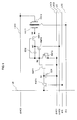
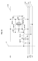
- Fig. 1 is a circuit diagram which shows a circuit structure of a single channel latch circuit (below referred to simply as latch circuit) of embodiment one of the present invention.
- the latch circuit of the present embodiment is a signal channel MOS transistor formed by only an n type MOS transistor (NMT*) (below referred to simply as transistor).
- the n type MOS transistor (NMT*) of the present embodiment is a thin film transistor (below referred to as a-Si transistor) including amorphous silicon semiconductor layers.
- CD1, CD2 are capacitors
- LD is a data line
- LG is a scanning line
- LAC 1 is a first latch control line receiving a first drive clock ( ⁇ AC1)
- LAC2 is a second latch control line receiving a second drive clock ( ⁇ AC2)
- LAC3 is a third latch control line receiving a third drive clock ( ⁇ AC3).
- a circuit which uses charging and discharging of a capacitor
- either increasing the gate width of a transistor and increasing the total amount of current flow, or increasing a gate voltage and increasing the amount of current per unit surface area are general methods which use an a-Si transistor which has a small amount of movement and which secures a desired operation speed.
- a desired operation speed is realized by increasing the gate voltage and increasing the amount of current per unit surface area.
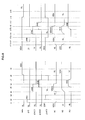
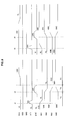
- Fig. 2 is a timing chart which shows the time changes of a scanning voltage ( ⁇ G), drive clock ( ⁇ AC1 ⁇ AC3), and each node (N1, N2, N3 and N4) of the latch circuit shown in Fig. 1 .
- a scanning voltage ( ⁇ G) (what is called a programming pulse (gate pulse)) on a scan line (LG) changes from a Low level voltage (referred to as L level below) VL to a High level voltage (below referred to a H level) VH1 (also called "a scanning voltage is input”)
- a scanning voltage ⁇ G
- gate pulse gate pulse
- NMT1 an input transistor
- the H level voltage VH1 of the scanning voltage ( ⁇ G) is a high voltage about 10V higher than the H level voltage VHD on the data line (LD) to match the transistor size of the transistor (NMT1). In the present embodiment, it is preferred that the voltage VH1 is 15V or more.
- the third drive clock ( ⁇ AC3) on the third latch control line (LAC3) changes from a H level voltage VH3 to a L level voltage VL (for example 0V).
- VH3 a H level voltage
- VL a L level voltage
- the position of the shutter (S) moves to an intermediate position between the first output (OUT1) and second output (OUT2) with the force of a spring.
- VH4 of the node (N2) is expresses by the following equation (1).
- VH ⁇ 4 VH ⁇ 2 - Vth
- Vth is a threshold voltage of the transistor (NMT3).
- NMT3 threshold voltage of the transistor
- VH2 when a voltage VH2 is set at 25V and an effective Vth added with a charge time of a charge capacitor is set at 5V, VH4 becomes around 20V using equation (1).
- the threshold voltages of all the n type MOS transistors are given as Vth for the purpose of simplification.
- VDH3 VL + VH ⁇ 2 X CD ⁇ 1 / CD ⁇ 1 + CN ⁇ 1 ⁇ S
- CN 1S is what is called a parasitic capacitance calculated by subtracting a capacitance (CD1) from the capacitance of the node (N1).
- the transistor (NMT4) becomes an on state.
- VH ⁇ 2 VH ⁇ 4 + VN ⁇ 3 X CD ⁇ 2 / CD ⁇ 2 + CN ⁇ 2 ⁇ S
- VN3 is the voltage of the node (N3)
- CN2S is a value calculated by subtracting a capacitance (CD2) from the capacitance of the node (N2), that is, parasitic capacitance of node (N2).
- VH ⁇ 4 ⁇ ⁇ VH ⁇ 4 + VH ⁇ 2 X CD ⁇ 2 / CD ⁇ 2 + CN ⁇ 2 ⁇ S
- the voltage VH4' is a gate voltage with respect to the transistor (NMT5)
- the voltage of the node (N4) also becomes the voltage VH2.
- the node (N3) and node (N4) both become 25V.
- the transistor (NMT3) is diode-connected, a current does not flow from the node (N2) to the first latch control line (LAC1). Therefore, the node (N2) maintains a voltage VH4'. Furthermore, exactly speaking, because the gate of the transistor (NMT2) changes from an H level to a L level, there is a small drop in voltage due to capacitance between the gate/drain of the transistor (NMT2), however, this change is so minimal that it is ignored in the present description.
- the voltage of the nodes (N3, N4) drops according to a voltage drop of the second drive clock ( ⁇ AC2).
- the voltage VN2 of the node (N2) also drops according to the equation (3).
- the voltage (VN2) of the node (N2) is a voltage VH4, and the transistors (NMT4, NMT5) become a sufficiently low resistance on state. Therefore, the nodes (N3, N4) become a L level voltage VL during a relatively short time period.
- the first output (OUT1) is set to a Low level voltage VL by the drive method described above. Therefore, when the latch circuit of the present embodiment is used in the movable shutter type display described above, the shutter (S) is attracted to the first output (OUT1) side between the time (t6) and (t7) by an electrostatic force. However, after time (t7), the shutter (S) is no longer attracted to the first output (OUT1) side by an electrostatic force. Therefore, the shutter (S) is positioned for example between the first output (OUT1) and second output (OUT2) by a spring force which supports the shutter (S).
- a scanning voltage ( ⁇ G) on a scan line (LG) changes from a L level voltage VL to a H level voltage VH1
- an input transistor (NMT1) is switched on and the voltage of the node (N1) becomes the voltage (data: voltage VDH at time (t11)) on the data line (LD).
- the voltage VDH is higher than the threshold voltage Vth of the transistor (NMT2), the voltage of the node (N2) flows at a desired time period, and is set to a voltage which can be set to the voltage VL, 7V for example.
- the transistor (NMT2) becomes an on state and the voltage of the node (N2) becomes a voltage from VH4 to VL.
- the transistor (NMT4) changes to an off state from an on state due to gate capacitance between the capacitor (CD2) and transistor (NMT4)
- the voltage of the node (N3) becomes a voltage slightly on the minus side.
- this is so minimal that it is ignored in Fig. 2 .
- the transistor (NMT5) there is no capacitance coupling such as the capacitor (CD2), and because there is only a small gate capacitance of the transistor (NMT5), this is also ignored in Fig. 2 .
- the third drive clock ( ⁇ AC3) on the third latch control line (LAC3) changes from a H level voltage VH3 to a L level voltage VL.
- the position of the shutter (S) moves to an intermediate position between the first output (OUT1) and the second output (OUT2) by the force of a spring.
- the first drive clock ( ⁇ AC1) on the first latch control line (LAC1) changes from a L level voltage VL to a H level voltage VH2.
- VDH ⁇ 13 VDH + VH ⁇ 2 X CD ⁇ 1 / CD ⁇ 1 + CN ⁇ 1 ⁇ S
- the first drive clock ( ⁇ AC1) on the first latch control line (LAC1) changes from a H level voltage VH2 to a L level voltage VL.
- the transistor (NMT2) is in an on state, the voltage of the node (N2) changes from the voltage VH4' to VL.
- the transistors (NMT4) and (NMT5) are switched off.
- the second drive clock ( ⁇ AC2) on the second latch control line (LAC2) changes from a H level voltage VH2 to a L level voltage VL.
- VH ⁇ 12 VH ⁇ 2 - VH ⁇ 4 ⁇ ⁇ X CD ⁇ 2 + CGD ⁇ 4 / CD ⁇ 2 + CGD ⁇ 4 + CN ⁇ 2 ⁇ S
- CGD4 is the gate/drain capacitance of the transistor (NMT4)
- CN2S is the parasitic capacitance other than the capacitor (CD2) of the node (N2) and the gate/drain capacitance (CGD4) of the transistor (NMT4).
- the capacitor CD2 has a relatively large capacitance compared to the parasitic capacitance (CN2S, CN3S), and therefore, it is preferred to take up around 80% of the capacitance of the node (N2).
- VH12 provided in equation (8) sometimes changes to a significantly low voltage.
- VH4 20V via equation (1)
- VH4' 40V via equation (5)
- the voltage of the node (N4) receives an influence of the change of the node (N2).
- the capacitance coupling at this time is only the capacitance between the gate/drain of the transistor (NMT5), the ratio which is taken up with respect to the capacitance of the node (N4) including a load of the first output (OUT1) is small and therefore the drop in voltage is small and it is possible to maintain a required voltage for a shutter operation.
- Fig. 3 is a block diagram which shows an approximate structure of a display (movable shutter type display) which displays an image by electrically controlling the position of the movable shutter (S) of embodiment one of the present invention.
- the movable shutter type display shown in Fig. 3 is arranged two dimensionally in one pixel (PX), and the circuit shown in Fig. 1 is also arranged in each pixel.
- a scan line (LG) is arranged in row units and is input to a perpendicular drive circuit (XDR).
- a data line is arranged in column units and is input to a horizontal drive circuit (YDR).
- the first latch control line (LAC1), second latch control line (LAC2), third latch control line (LAC3), and shutter control line (LSS) are commonly arranged on each pixel and input to the horizontal drive circuit (YDR).
- a programming time period (TA in Fig, 2 )
- the movable shutter (S) is moved to the first output (OUT1) or second output (OUT2) side in a movable shutter state setting time period (TB in Fig. 2 ) and an image is displayed in a display time period (TC in Fig. 2 ).
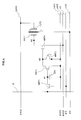
- Fig. 4 is a circuit diagram which shows a circuit structure of a single channel latch circuit of embodiment two of the present invention
- the latch circuit shown in Fig. 4 does not include the capacitor (CD2) and transistor (NMT5) of the latch circuit shown in Fig. 1 and the node (N3) is the first output (OUT1).
- the voltage VH1 is a voltage of 15V or more the same as in embodiment one described above.
- the third drive clock ( ⁇ AC3) on the third latch control line (LAC3) changes from a H level voltage VH3 to a L level voltage VL.
- the position of the shutter (S) moves to an intermediate position between the first output (OUT1) and second output (OUT2) with the force of a spring.
- Vth is a threshold voltage of the transistor (NMT3).
- the transistor (NMT4) becomes an on state.
- the final voltage of the node (N3) can be set as the voltage VH2 which is the H level voltage of the second drive clock ( ⁇ AC2).
- the transistor (NMT3) is diode-connected, a current does not flow from the node (N2) to the first latch control line (LAC1). Therefore, the node (N2) maintains a voltage VH4. Furthermore, exactly speaking, because the gate of the transistor (NMT2) changes from an H level voltage to a L level voltage, there is a small drop in voltage due to capacitance between the gate/drain of the transistor (NMT2), however, this change is so minimal that it is ignored in the present description.
- the voltage of the node (N3) drops according to a voltage drop of the second drive clock ( ⁇ AC2).
- the voltage of the node (N2) is a voltage VH4, and the transistor (NMT4) becomes at a sufficiently low resistance on state. Therefore, the node (N3) becomes at a L level voltage VL during a relatively short time period.
- the first output (OUT1) is set to a Low level voltage VL by the drive method described above. Therefore, when the latch circuit of the present embodiment is used in the movable shutter type display described above, the shutter (S) is attracted to the first output (OUT1) side between the time (t6) and (t7) by an electrostatic force. However, after time (t7), the shutter (S) is no longer attracted to the first output (OUT1) side by an electrostatic force. Therefore, the shutter (S) is positioned for example between the first output (OUT1) and second output (OUT2) by a spring force which supports the shutter (S).
- a scanning voltage ( ⁇ G) on a scan line (LG) changes from a L level voltage VL to a H level voltage VH1
- an input transistor (NMT1) is switched on and the voltage of the node (N1) becomes the voltage (data: voltage VDH at time (t11)) on the data line (LD).
- the voltage VDH is higher than the threshold voltage Vth of the transistor (NMT2)
- the voltage of the node (N2) flows at a desired time period, and is set to a voltage which can be set to the voltage VL, 7V for example.
- the transistor (NMT2) becomes an on state, and the voltage of the node (N2) becomes a voltage from VH4 to VL.
- the third drive clock ( ⁇ AC3) on the third latch control line (LAC3) changes from a H level voltage VH3 to a L level voltage VL.
- the position of the shutter (S) moves to an intermediate position between the first output (OUT1) and the second output (OUT2) by the force of a spring.
- the first drive clock ( ⁇ AC1) on the first latch control line (LAC1) changes from a L level voltage VL to a H level voltage VH2'.
- the first drive clock ( ⁇ AC1) on the first latch control line (LAC1) changes from a H level voltage VH2' to a L level voltage VL.
- the transistor (NMT2) is in an on state, the voltage of the node (N2) changes from the voltage VH4 to VL. As a result, the transistor (NMT4) is switched off.
- the shutter (S) moves to the first output (OUT1) side by an electrostatic force at the point where the voltage of the node (N3) becomes a H level, and this state is maintained.
- n type MOS transistor using a thin film transistor including amorphous silicon semiconductor layers was explained above.
- a thin film transistor including polysilicon semiconductor layers it is also possible to use a thin film transistor including polysilicon semiconductor layers as the n type MOS transistor.
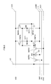
- a scanning voltage ( ⁇ G) on a scan line (LG) changes from a H level voltage VH to a L level voltage VL1 (also called “a scanning voltage is input")
- an input transistor (PMT1) is switched on and the voltage of the node (N1) becomes the voltage (data: voltage VDL at time (t1)) on the data line (LD).
- the third drive clock ( ⁇ AC3) on the third latch control line (LAC3) changes from a H level voltage VH to a L level voltage VL3.
- the position of the shutter (S) moves to an intermediate position between the first output (OUT1) and second output (OUT2) with the force of a spring.
- Vth is a threshold voltage of the transistor (PMT3).
- the transistor (PMT4) becomes an on state.
- the final voltage of the node (N3) can be set as the voltage VL3 which is the L level voltage of the second drive clock ( ⁇ AC2).
- the transistor (PMT3) is diode-connected, a current does not flow from the first latch control line (LAC1) to the node (N2). Therefore, the node (N2) is charged via the transistor (PMT2) and becomes at a voltage VH.
- the transistor (PMT4) is switched off. Furthermore, exactly speaking, because the gate of the transistor (PMT2) changes from an L level voltage to H level voltage, there is a small rise in voltage due to capacitance between the gate/drain of the transistor (PMT2), however, this change is so minimal that it is ignored in the present description.
- the third drive clock ( ⁇ AC3) on the third latch control line (LAC3) is changed from a H level voltage VH to a L level voltage VL3.
- the position of the shutter (S) moves to an intermediate position between the first output (OUT1) and the second output (OUT2) by the force of a spring.
- the first drive clock ( ⁇ AC1) on the first latch control line (LAC1) changes from a H level voltage VH to a L level voltage VL2.
- the voltage of the node (N1) immediately before is VH
- the first drive clock ( ⁇ AC1) on the first latch control line (LAC1) changes from a L level voltage VL2 to a H level voltage VH.
- the transistor (PMT2) is in an off state, and because the transistor (PMT3) is diode-connected, a current does not flow from the first latch control line (LAC1) to the node (N2). Therefore, the node (N2) maintains a voltage VL4.
- the gate of the transistor (PMT2) changes from an L level to a H level, there is a small rise in voltage due to capacitance between the gate/drain of the transistor (PMT2), however, this change is so minimal that it is ignored in the present description.
- the shutter (S) moves to the first output (OUT1) side by an electrostatic force at the point where the voltage of the node (N4) becomes a H level, and this state is maintained.
- the latch circuit of the present invention is used in a movable shutter type display was explained.
- the present invention can also be applied to other displays which required similar operations other than a circuit of a movable shutter type display.
Landscapes
- Engineering & Computer Science (AREA)
- Physics & Mathematics (AREA)
- Computer Hardware Design (AREA)
- General Physics & Mathematics (AREA)
- Theoretical Computer Science (AREA)
- Control Of Indicators Other Than Cathode Ray Tubes (AREA)
- Liquid Crystal Display Device Control (AREA)
Applications Claiming Priority (1)
| Application Number | Priority Date | Filing Date | Title |
|---|---|---|---|
| JP2011106895A JP2012239046A (ja) | 2011-05-12 | 2011-05-12 | ラッチ回路およびラッチ回路を用いた表示装置 |
Publications (2)
| Publication Number | Publication Date |
|---|---|
| EP2523348A1 EP2523348A1 (en) | 2012-11-14 |
| EP2523348B1 true EP2523348B1 (en) | 2015-07-08 |
Family
ID=45932184
Family Applications (1)
| Application Number | Title | Priority Date | Filing Date |
|---|---|---|---|
| EP12161034.9A Not-in-force EP2523348B1 (en) | 2011-05-12 | 2012-03-23 | Latch circuit and display device using the latch circuit |
Country Status (6)
| Country | Link |
|---|---|
| US (1) | US8994704B2 (enExample) |
| EP (1) | EP2523348B1 (enExample) |
| JP (1) | JP2012239046A (enExample) |
| KR (1) | KR101383865B1 (enExample) |
| CN (1) | CN102780471B (enExample) |
| TW (1) | TWI457903B (enExample) |
Families Citing this family (7)
| Publication number | Priority date | Publication date | Assignee | Title |
|---|---|---|---|---|
| JP5856799B2 (ja) * | 2011-10-17 | 2016-02-10 | ピクストロニクス,インコーポレイテッド | ラッチ回路および表示装置 |
| JP2014142405A (ja) * | 2013-01-22 | 2014-08-07 | Pixtronix Inc | 画素回路およびそれを備えた表示装置 |
| CN103986455B (zh) * | 2014-05-09 | 2017-04-12 | 三星半导体(中国)研究开发有限公司 | 扫描保持寄存器 |
| US10071904B2 (en) | 2014-09-25 | 2018-09-11 | Semiconductor Energy Laboratory Co., Ltd. | Semiconductor device, display module, and electronic device |
| US9698170B2 (en) | 2014-10-07 | 2017-07-04 | Semiconductor Energy Laboratory Co., Ltd. | Semiconductor device, display module, and electronic device |
| US10068927B2 (en) | 2014-10-23 | 2018-09-04 | Semiconductor Energy Laboratory Co., Ltd. | Semiconductor device, display module, and electronic device |
| CN107403611B (zh) * | 2017-09-25 | 2020-12-04 | 京东方科技集团股份有限公司 | 像素记忆电路、液晶显示器和可穿戴设备 |
Family Cites Families (9)
| Publication number | Priority date | Publication date | Assignee | Title |
|---|---|---|---|---|
| JP4296492B2 (ja) * | 2003-12-01 | 2009-07-15 | ソニー株式会社 | ラッチ回路、シフトレジスタ回路、表示装置の駆動回路、表示装置 |
| JP2005195854A (ja) * | 2004-01-07 | 2005-07-21 | Mitsubishi Electric Corp | 画像表示装置およびその検査方法 |
| KR20050075116A (ko) | 2004-01-15 | 2005-07-20 | 매그나칩 반도체 유한회사 | 디스플레이 패널을 위한 래치 회로 |
| GB0412586D0 (en) * | 2004-06-05 | 2004-07-07 | Koninkl Philips Electronics Nv | Active matrix display devices |
| EP2116885B1 (en) | 2005-02-23 | 2014-07-23 | Pixtronix, Inc. | Display methods and apparatus |
| US9158106B2 (en) | 2005-02-23 | 2015-10-13 | Pixtronix, Inc. | Display methods and apparatus |
| JP2008164796A (ja) | 2006-12-27 | 2008-07-17 | Sony Corp | 画素回路および表示装置とその駆動方法 |
| JP5151585B2 (ja) | 2008-03-18 | 2013-02-27 | ソニー株式会社 | 半導体デバイス、表示パネル及び電子機器 |
| GB2459661A (en) * | 2008-04-29 | 2009-11-04 | Sharp Kk | A low power NMOS latch for an LCD scan pulse shift register |
-
2011
- 2011-05-12 JP JP2011106895A patent/JP2012239046A/ja active Pending
-
2012
- 2012-03-23 EP EP12161034.9A patent/EP2523348B1/en not_active Not-in-force
- 2012-03-23 TW TW101110255A patent/TWI457903B/zh not_active IP Right Cessation
- 2012-03-26 CN CN201210082438.XA patent/CN102780471B/zh not_active Expired - Fee Related
- 2012-03-26 KR KR1020120030701A patent/KR101383865B1/ko not_active Expired - Fee Related
- 2012-03-26 US US13/429,476 patent/US8994704B2/en not_active Expired - Fee Related
Also Published As
| Publication number | Publication date |
|---|---|
| TWI457903B (zh) | 2014-10-21 |
| KR20120127202A (ko) | 2012-11-21 |
| JP2012239046A (ja) | 2012-12-06 |
| TW201246167A (en) | 2012-11-16 |
| US20120287101A1 (en) | 2012-11-15 |
| EP2523348A1 (en) | 2012-11-14 |
| CN102780471B (zh) | 2015-10-14 |
| KR101383865B1 (ko) | 2014-04-10 |
| CN102780471A (zh) | 2012-11-14 |
| US8994704B2 (en) | 2015-03-31 |
Similar Documents
| Publication | Publication Date | Title |
|---|---|---|
| EP2523348B1 (en) | Latch circuit and display device using the latch circuit | |
| US20210166632A1 (en) | Pixel unit circuit, pixel circuit, method for driving pixel circuit and display device | |
| US9905311B2 (en) | Shift register circuit, drive circuit, and display device | |
| KR101552420B1 (ko) | 주사 신호선 구동 회로, 그것을 구비한 표시 장치 및 주사 신호선의 구동 방법 | |
| US8194817B2 (en) | Shift register circuit | |
| US8605029B2 (en) | Shift register, display device provided with same, and method of driving shift register | |
| JP5851594B2 (ja) | Mems表示デバイス用のラッチ回路 | |
| US20160247442A1 (en) | Gate drive circuit | |
| US20110001732A1 (en) | Shift register circuit, display device, and method for driving shift register circuit | |
| US10923064B2 (en) | Scanning signal line drive circuit and display device equipped with same | |
| US20140035891A1 (en) | Scanning signal line drive circuit, display device having the same, and drive method for scanning signal line | |
| EP4303859A1 (en) | Pixel driving circuit and display panel | |
| KR20020069241A (ko) | 액티브 매트릭스형 표시 장치 및 액티브 매트릭스형 유기일렉트로 루미네센스 표시 장치 | |
| CN103038811B (zh) | 显示装置 | |
| US9293099B2 (en) | Display drive circuit, display panel, and display device | |
| CN109887469B (zh) | 移位寄存器及具备该移位寄存器的显示装置 | |
| US20200394976A1 (en) | Scanning signal line drive circuit and display device provided with same | |
| US9099997B2 (en) | Latch circuit and display device | |
| US7573451B2 (en) | Sample hold circuit and image display device using the same | |
| JP2014127221A (ja) | シフトレジスタ回路および画像表示装置 | |
| US20100073061A1 (en) | Inverter circuit |
Legal Events
| Date | Code | Title | Description |
|---|---|---|---|
| PUAI | Public reference made under article 153(3) epc to a published international application that has entered the european phase |
Free format text: ORIGINAL CODE: 0009012 |
|
| 17P | Request for examination filed |
Effective date: 20120723 |
|
| AK | Designated contracting states |
Kind code of ref document: A1 Designated state(s): AL AT BE BG CH CY CZ DE DK EE ES FI FR GB GR HR HU IE IS IT LI LT LU LV MC MK MT NL NO PL PT RO RS SE SI SK SM TR |
|
| AX | Request for extension of the european patent |
Extension state: BA ME |
|
| RAP1 | Party data changed (applicant data changed or rights of an application transferred) |
Owner name: JAPAN DISPLAY INC. |
|
| RAP1 | Party data changed (applicant data changed or rights of an application transferred) |
Owner name: PIXTRONIX, INC. |
|
| GRAP | Despatch of communication of intention to grant a patent |
Free format text: ORIGINAL CODE: EPIDOSNIGR1 |
|
| INTG | Intention to grant announced |
Effective date: 20150129 |
|
| GRAS | Grant fee paid |
Free format text: ORIGINAL CODE: EPIDOSNIGR3 |
|
| GRAA | (expected) grant |
Free format text: ORIGINAL CODE: 0009210 |
|
| AK | Designated contracting states |
Kind code of ref document: B1 Designated state(s): AL AT BE BG CH CY CZ DE DK EE ES FI FR GB GR HR HU IE IS IT LI LT LU LV MC MK MT NL NO PL PT RO RS SE SI SK SM TR |
|
| REG | Reference to a national code |
Ref country code: GB Ref legal event code: FG4D |
|
| REG | Reference to a national code |
Ref country code: AT Ref legal event code: REF Ref document number: 736078 Country of ref document: AT Kind code of ref document: T Effective date: 20150715 Ref country code: CH Ref legal event code: EP |
|
| REG | Reference to a national code |
Ref country code: IE Ref legal event code: FG4D |
|
| REG | Reference to a national code |
Ref country code: DE Ref legal event code: R096 Ref document number: 602012008508 Country of ref document: DE |
|
| REG | Reference to a national code |
Ref country code: AT Ref legal event code: MK05 Ref document number: 736078 Country of ref document: AT Kind code of ref document: T Effective date: 20150708 |
|
| REG | Reference to a national code |
Ref country code: NL Ref legal event code: MP Effective date: 20150708 |
|
| REG | Reference to a national code |
Ref country code: LT Ref legal event code: MG4D |
|
| PG25 | Lapsed in a contracting state [announced via postgrant information from national office to epo] |
Ref country code: LV Free format text: LAPSE BECAUSE OF FAILURE TO SUBMIT A TRANSLATION OF THE DESCRIPTION OR TO PAY THE FEE WITHIN THE PRESCRIBED TIME-LIMIT Effective date: 20150708 Ref country code: GR Free format text: LAPSE BECAUSE OF FAILURE TO SUBMIT A TRANSLATION OF THE DESCRIPTION OR TO PAY THE FEE WITHIN THE PRESCRIBED TIME-LIMIT Effective date: 20151009 Ref country code: NO Free format text: LAPSE BECAUSE OF FAILURE TO SUBMIT A TRANSLATION OF THE DESCRIPTION OR TO PAY THE FEE WITHIN THE PRESCRIBED TIME-LIMIT Effective date: 20151008 Ref country code: FI Free format text: LAPSE BECAUSE OF FAILURE TO SUBMIT A TRANSLATION OF THE DESCRIPTION OR TO PAY THE FEE WITHIN THE PRESCRIBED TIME-LIMIT Effective date: 20150708 Ref country code: LT Free format text: LAPSE BECAUSE OF FAILURE TO SUBMIT A TRANSLATION OF THE DESCRIPTION OR TO PAY THE FEE WITHIN THE PRESCRIBED TIME-LIMIT Effective date: 20150708 |
|
| PG25 | Lapsed in a contracting state [announced via postgrant information from national office to epo] |
Ref country code: RS Free format text: LAPSE BECAUSE OF FAILURE TO SUBMIT A TRANSLATION OF THE DESCRIPTION OR TO PAY THE FEE WITHIN THE PRESCRIBED TIME-LIMIT Effective date: 20150708 Ref country code: AT Free format text: LAPSE BECAUSE OF FAILURE TO SUBMIT A TRANSLATION OF THE DESCRIPTION OR TO PAY THE FEE WITHIN THE PRESCRIBED TIME-LIMIT Effective date: 20150708 Ref country code: PL Free format text: LAPSE BECAUSE OF FAILURE TO SUBMIT A TRANSLATION OF THE DESCRIPTION OR TO PAY THE FEE WITHIN THE PRESCRIBED TIME-LIMIT Effective date: 20150708 Ref country code: PT Free format text: LAPSE BECAUSE OF FAILURE TO SUBMIT A TRANSLATION OF THE DESCRIPTION OR TO PAY THE FEE WITHIN THE PRESCRIBED TIME-LIMIT Effective date: 20151109 Ref country code: ES Free format text: LAPSE BECAUSE OF FAILURE TO SUBMIT A TRANSLATION OF THE DESCRIPTION OR TO PAY THE FEE WITHIN THE PRESCRIBED TIME-LIMIT Effective date: 20150708 Ref country code: SE Free format text: LAPSE BECAUSE OF FAILURE TO SUBMIT A TRANSLATION OF THE DESCRIPTION OR TO PAY THE FEE WITHIN THE PRESCRIBED TIME-LIMIT Effective date: 20150708 Ref country code: HR Free format text: LAPSE BECAUSE OF FAILURE TO SUBMIT A TRANSLATION OF THE DESCRIPTION OR TO PAY THE FEE WITHIN THE PRESCRIBED TIME-LIMIT Effective date: 20150708 Ref country code: IS Free format text: LAPSE BECAUSE OF FAILURE TO SUBMIT A TRANSLATION OF THE DESCRIPTION OR TO PAY THE FEE WITHIN THE PRESCRIBED TIME-LIMIT Effective date: 20151108 |
|
| REG | Reference to a national code |
Ref country code: DE Ref legal event code: R097 Ref document number: 602012008508 Country of ref document: DE |
|
| PG25 | Lapsed in a contracting state [announced via postgrant information from national office to epo] |
Ref country code: DK Free format text: LAPSE BECAUSE OF FAILURE TO SUBMIT A TRANSLATION OF THE DESCRIPTION OR TO PAY THE FEE WITHIN THE PRESCRIBED TIME-LIMIT Effective date: 20150708 Ref country code: EE Free format text: LAPSE BECAUSE OF FAILURE TO SUBMIT A TRANSLATION OF THE DESCRIPTION OR TO PAY THE FEE WITHIN THE PRESCRIBED TIME-LIMIT Effective date: 20150708 Ref country code: CZ Free format text: LAPSE BECAUSE OF FAILURE TO SUBMIT A TRANSLATION OF THE DESCRIPTION OR TO PAY THE FEE WITHIN THE PRESCRIBED TIME-LIMIT Effective date: 20150708 Ref country code: SK Free format text: LAPSE BECAUSE OF FAILURE TO SUBMIT A TRANSLATION OF THE DESCRIPTION OR TO PAY THE FEE WITHIN THE PRESCRIBED TIME-LIMIT Effective date: 20150708 Ref country code: IT Free format text: LAPSE BECAUSE OF FAILURE TO SUBMIT A TRANSLATION OF THE DESCRIPTION OR TO PAY THE FEE WITHIN THE PRESCRIBED TIME-LIMIT Effective date: 20150708 |
|
| PLBE | No opposition filed within time limit |
Free format text: ORIGINAL CODE: 0009261 |
|
| STAA | Information on the status of an ep patent application or granted ep patent |
Free format text: STATUS: NO OPPOSITION FILED WITHIN TIME LIMIT |
|
| PG25 | Lapsed in a contracting state [announced via postgrant information from national office to epo] |
Ref country code: RO Free format text: LAPSE BECAUSE OF FAILURE TO SUBMIT A TRANSLATION OF THE DESCRIPTION OR TO PAY THE FEE WITHIN THE PRESCRIBED TIME-LIMIT Effective date: 20150708 |
|
| PGFP | Annual fee paid to national office [announced via postgrant information from national office to epo] |
Ref country code: GB Payment date: 20160224 Year of fee payment: 5 |
|
| 26N | No opposition filed |
Effective date: 20160411 |
|
| PGFP | Annual fee paid to national office [announced via postgrant information from national office to epo] |
Ref country code: DE Payment date: 20160324 Year of fee payment: 5 |
|
| PG25 | Lapsed in a contracting state [announced via postgrant information from national office to epo] |
Ref country code: SI Free format text: LAPSE BECAUSE OF FAILURE TO SUBMIT A TRANSLATION OF THE DESCRIPTION OR TO PAY THE FEE WITHIN THE PRESCRIBED TIME-LIMIT Effective date: 20150708 Ref country code: BE Free format text: LAPSE BECAUSE OF NON-PAYMENT OF DUE FEES Effective date: 20160331 |
|
| PG25 | Lapsed in a contracting state [announced via postgrant information from national office to epo] |
Ref country code: LU Free format text: LAPSE BECAUSE OF FAILURE TO SUBMIT A TRANSLATION OF THE DESCRIPTION OR TO PAY THE FEE WITHIN THE PRESCRIBED TIME-LIMIT Effective date: 20160323 Ref country code: MC Free format text: LAPSE BECAUSE OF FAILURE TO SUBMIT A TRANSLATION OF THE DESCRIPTION OR TO PAY THE FEE WITHIN THE PRESCRIBED TIME-LIMIT Effective date: 20150708 |
|
| REG | Reference to a national code |
Ref country code: CH Ref legal event code: PL |
|
| REG | Reference to a national code |
Ref country code: GB Ref legal event code: 732E Free format text: REGISTERED BETWEEN 20161027 AND 20161102 |
|
| REG | Reference to a national code |
Ref country code: IE Ref legal event code: MM4A |
|
| PG25 | Lapsed in a contracting state [announced via postgrant information from national office to epo] |
Ref country code: BE Free format text: LAPSE BECAUSE OF FAILURE TO SUBMIT A TRANSLATION OF THE DESCRIPTION OR TO PAY THE FEE WITHIN THE PRESCRIBED TIME-LIMIT Effective date: 20150708 |
|
| REG | Reference to a national code |
Ref country code: FR Ref legal event code: ST Effective date: 20161130 |
|
| REG | Reference to a national code |
Ref country code: DE Ref legal event code: R082 Ref document number: 602012008508 Country of ref document: DE Representative=s name: MAUCHER JENKINS, DE Ref country code: DE Ref legal event code: R081 Ref document number: 602012008508 Country of ref document: DE Owner name: SNAPTRACK, INC., SAN DIEGO, US Free format text: FORMER OWNER: PIXTRONIX, INC., SAN DIEGO, CALIF., US Ref country code: DE Ref legal event code: R082 Ref document number: 602012008508 Country of ref document: DE Representative=s name: MAUCHER JENKINS PATENTANWAELTE & RECHTSANWAELT, DE |
|
| PG25 | Lapsed in a contracting state [announced via postgrant information from national office to epo] |
Ref country code: LI Free format text: LAPSE BECAUSE OF NON-PAYMENT OF DUE FEES Effective date: 20160331 Ref country code: FR Free format text: LAPSE BECAUSE OF NON-PAYMENT OF DUE FEES Effective date: 20160331 Ref country code: CH Free format text: LAPSE BECAUSE OF NON-PAYMENT OF DUE FEES Effective date: 20160331 Ref country code: IE Free format text: LAPSE BECAUSE OF NON-PAYMENT OF DUE FEES Effective date: 20160323 |
|
| PG25 | Lapsed in a contracting state [announced via postgrant information from national office to epo] |
Ref country code: NL Free format text: LAPSE BECAUSE OF FAILURE TO SUBMIT A TRANSLATION OF THE DESCRIPTION OR TO PAY THE FEE WITHIN THE PRESCRIBED TIME-LIMIT Effective date: 20150708 |
|
| PG25 | Lapsed in a contracting state [announced via postgrant information from national office to epo] |
Ref country code: MT Free format text: LAPSE BECAUSE OF FAILURE TO SUBMIT A TRANSLATION OF THE DESCRIPTION OR TO PAY THE FEE WITHIN THE PRESCRIBED TIME-LIMIT Effective date: 20150708 |
|
| REG | Reference to a national code |
Ref country code: DE Ref legal event code: R119 Ref document number: 602012008508 Country of ref document: DE |
|
| GBPC | Gb: european patent ceased through non-payment of renewal fee |
Effective date: 20170323 |
|
| PG25 | Lapsed in a contracting state [announced via postgrant information from national office to epo] |
Ref country code: DE Free format text: LAPSE BECAUSE OF NON-PAYMENT OF DUE FEES Effective date: 20171003 |
|
| PG25 | Lapsed in a contracting state [announced via postgrant information from national office to epo] |
Ref country code: GB Free format text: LAPSE BECAUSE OF NON-PAYMENT OF DUE FEES Effective date: 20170323 |
|
| PG25 | Lapsed in a contracting state [announced via postgrant information from national office to epo] |
Ref country code: SM Free format text: LAPSE BECAUSE OF FAILURE TO SUBMIT A TRANSLATION OF THE DESCRIPTION OR TO PAY THE FEE WITHIN THE PRESCRIBED TIME-LIMIT Effective date: 20150708 Ref country code: CY Free format text: LAPSE BECAUSE OF FAILURE TO SUBMIT A TRANSLATION OF THE DESCRIPTION OR TO PAY THE FEE WITHIN THE PRESCRIBED TIME-LIMIT Effective date: 20150708 Ref country code: HU Free format text: LAPSE BECAUSE OF FAILURE TO SUBMIT A TRANSLATION OF THE DESCRIPTION OR TO PAY THE FEE WITHIN THE PRESCRIBED TIME-LIMIT; INVALID AB INITIO Effective date: 20120323 |
|
| PG25 | Lapsed in a contracting state [announced via postgrant information from national office to epo] |
Ref country code: MK Free format text: LAPSE BECAUSE OF FAILURE TO SUBMIT A TRANSLATION OF THE DESCRIPTION OR TO PAY THE FEE WITHIN THE PRESCRIBED TIME-LIMIT Effective date: 20150708 Ref country code: MT Free format text: LAPSE BECAUSE OF FAILURE TO SUBMIT A TRANSLATION OF THE DESCRIPTION OR TO PAY THE FEE WITHIN THE PRESCRIBED TIME-LIMIT Effective date: 20160331 Ref country code: TR Free format text: LAPSE BECAUSE OF FAILURE TO SUBMIT A TRANSLATION OF THE DESCRIPTION OR TO PAY THE FEE WITHIN THE PRESCRIBED TIME-LIMIT Effective date: 20150708 |
|
| PG25 | Lapsed in a contracting state [announced via postgrant information from national office to epo] |
Ref country code: BG Free format text: LAPSE BECAUSE OF FAILURE TO SUBMIT A TRANSLATION OF THE DESCRIPTION OR TO PAY THE FEE WITHIN THE PRESCRIBED TIME-LIMIT Effective date: 20150708 |
|
| PG25 | Lapsed in a contracting state [announced via postgrant information from national office to epo] |
Ref country code: AL Free format text: LAPSE BECAUSE OF FAILURE TO SUBMIT A TRANSLATION OF THE DESCRIPTION OR TO PAY THE FEE WITHIN THE PRESCRIBED TIME-LIMIT Effective date: 20150708 |