EP2515214A2 - Messvorrichtung und Sendeverfahren zum Messen der Berührungsposition auf der Anzeigetafel - Google Patents
Messvorrichtung und Sendeverfahren zum Messen der Berührungsposition auf der Anzeigetafel Download PDFInfo
- Publication number
- EP2515214A2 EP2515214A2 EP12002667A EP12002667A EP2515214A2 EP 2515214 A2 EP2515214 A2 EP 2515214A2 EP 12002667 A EP12002667 A EP 12002667A EP 12002667 A EP12002667 A EP 12002667A EP 2515214 A2 EP2515214 A2 EP 2515214A2
- Authority
- EP
- European Patent Office
- Prior art keywords
- sensing
- signal
- type sensing
- type
- input event
- Prior art date
- Legal status (The legal status is an assumption and is not a legal conclusion. Google has not performed a legal analysis and makes no representation as to the accuracy of the status listed.)
- Withdrawn
Links
Images


Classifications
-
- G—PHYSICS
- G06—COMPUTING OR CALCULATING; COUNTING
- G06F—ELECTRIC DIGITAL DATA PROCESSING
- G06F3/00—Input arrangements for transferring data to be processed into a form capable of being handled by the computer; Output arrangements for transferring data from processing unit to output unit, e.g. interface arrangements
- G06F3/01—Input arrangements or combined input and output arrangements for interaction between user and computer
- G06F3/03—Arrangements for converting the position or the displacement of a member into a coded form
- G06F3/041—Digitisers, e.g. for touch screens or touch pads, characterised by the transducing means
- G06F3/0412—Digitisers structurally integrated in a display
-
- G—PHYSICS
- G06—COMPUTING OR CALCULATING; COUNTING
- G06F—ELECTRIC DIGITAL DATA PROCESSING
- G06F3/00—Input arrangements for transferring data to be processed into a form capable of being handled by the computer; Output arrangements for transferring data from processing unit to output unit, e.g. interface arrangements
- G06F3/01—Input arrangements or combined input and output arrangements for interaction between user and computer
- G06F3/03—Arrangements for converting the position or the displacement of a member into a coded form
- G06F3/041—Digitisers, e.g. for touch screens or touch pads, characterised by the transducing means
- G06F3/0416—Control or interface arrangements specially adapted for digitisers
- G06F3/0418—Control or interface arrangements specially adapted for digitisers for error correction or compensation, e.g. based on parallax, calibration or alignment
- G06F3/04182—Filtering of noise external to the device and not generated by digitiser components
-
- G—PHYSICS
- G06—COMPUTING OR CALCULATING; COUNTING
- G06F—ELECTRIC DIGITAL DATA PROCESSING
- G06F3/00—Input arrangements for transferring data to be processed into a form capable of being handled by the computer; Output arrangements for transferring data from processing unit to output unit, e.g. interface arrangements
- G06F3/01—Input arrangements or combined input and output arrangements for interaction between user and computer
- G06F3/03—Arrangements for converting the position or the displacement of a member into a coded form
- G06F3/041—Digitisers, e.g. for touch screens or touch pads, characterised by the transducing means
- G06F3/042—Digitisers, e.g. for touch screens or touch pads, characterised by the transducing means by opto-electronic means
Definitions
- the present invention relates to a sensing apparatus and related sensing method for sensing a touch position on a display panel according to pre-characterizing clauses of claims 1 and 12.
- the in-cell touch technique is capable of reducing the production cost and improving the production yield, and applications thereof are also broadened.
- the photocurrent signal intensity may be affected by the process variation and the coupling noise interferences among the circuit elements, each of which may results from the chance cause (i.e., the random factor) and assignable chance (i.e., local factor).
- the accuracy of detecting the input event is degraded.
- the signal-to-noise (SNR) of the sensing unit has to be high enough to detect the input event correctly.
- the present invention aims at providing a sensing apparatus and a sensing method for sensing a touch position on a display panel to detect an input event (e.g. an illumination event) according to a difference between sensing signals for reducing the process variation and the signal coupling interference.
- an input event e.g. an illumination event
- the claimed sensing apparatus includes at least one sensing cell and a processing circuit.
- the sensing cell is disposed inside a display panel, and includes a first type sensing device and a second type sensing device.
- the first type sensing device is arranged to generate a first type sensing signal when the sensing cell receives an input event.
- the second type sensing device is adjacent to the first type sensing device, and arranged to generate a second type sensing signal when the sensing cell receives the input event, wherein a sensing ability of the first type sensing device to detect the input event is different from a sensing ability of the second type sensing device to detect the input event.
- the processing circuit is coupled to the sensing cell, and arranged for outputting a sensing output signal corresponding to the sensing cell according to a difference between the first type sensing signal and the second type sensing signal.
- the claimed sensing method includes following steps: when the display panel detects occurrence of an input event, generating a first type sensing signal corresponding to the input event based on a first sensing ability, and generating a second type sensing signal based on a second sensing ability different from the first sensing ability; and outputting a sensing output signal corresponding to the input event according to a difference between the first type sensing signal and the second type sensing signal.
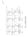
- the photo-sensing units PU_1-PU_n including photo-sensing devices PD_1-PD_n
- receive an input event e.g., an illumination event
- transistors M_1-M_n are conducted according to a gate control signal for transmitting photocurrent signals PI_1-PI_n to pads PAD_1-PAD_n, respectively.
- a backend processing circuit (not shown in FIG. 1 ) then processes the received photocurrent signals PI_1-PI_n, respectively, and accordingly determines light intensity received by each photo-sensing unit. As shown in FIG.
- each photocurrent signal may be affected by include noises N_1-N_4, which is generated from the common voltage node, the gate signal clock feedthrough, the source signal clock feedthrough, and the readout circuit common node (i.e., each pad), respectively.
- the photocurrent signal intensity of the sensing unit may be affected by at least one of the noises N_1-N_4, and thus is varied obviously with time. As a result, the signal-to-noise (SNR) of the sensing unit has to be high enough to detect the input event correctly.
- SNR signal-to-noise
- the concept of the present invention is to dispose at least two adjacent sensing devices disposed inside a display panel on a same sensing unit, wherein there is a sufficient difference in sensing abilities between the at least two adjacent sensing devices for detecting the same input event.
- the sensing unit may be applied to the in-cell photo-sensing touch, and the touch position information of the display panel is obtained by sensing brightness variations of touch positions.
- sensing signals generated due to the same input event in the at least two adjacent sensing devices respectively may be outputted in a differential manner, and the effects caused by the processing variation and the noise coupling can be greatly reduced in detecting the input event. Further description is detailed as follows.
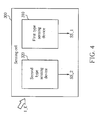
- FIG. 4 is a diagram illustrating a generalized sensing cell according to an embodiment of the present invention.
- the sensing cell 300 includes, but is not limited to, a first type sensing device 310 and a second type sensing device 320.
- the first type sensing device 310 is disposed inside a display panel (not shown in FIG. 4 ), and arranged to generate a first type sensing signal SS_1 according to an input event I_E when the sensing cell 300 receives the input event I_E.
- the second type sensing device 320 is also disposed inside the display panel, and arranged to generate a second type sensing signal SS_2 not according to the input event I_E when the sensing cell 300 receives the input event I_E.
- the second type sensing device 320 is adjacent to the first type sensing device 310, the first type sensing device 310 and the second type sensing device 320 are affected by substantially the same local factor of the aforementioned process variation and/or noise coupling. It should be noted that the second type sensing device 320 generates the second type sensing signal SS_2 not according to the received input event I_E. In one implementation, with proper design, the second type sensing device 320 may not receive an input signal of the input event I_E, or ignore the input signal even after receiving the input signal of the input event L_E.
- the second type sensing device 320 may obstruct the path used to receive the input signal, or eliminate the input signal by the inner material and/or the architecture design thereof. Moreover, the first type sensing device 310 and the second type sensing device 320 may have different architectures to achieve the sufficient difference in sensing responses on the same input event I_E therebetween.
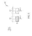
- FIG. 5 is a diagram illustrating an exemplary sensing cell according to a first embodiment of the present invention.
- the exemplary sensing cell 400 includes, but is not limited to, a first type sensing device 410 and a second type sensing device 420, wherein the first type sensing device 410 and the second type sensing device 420 are both disposed inside a display panel (not shown in FIG. 5 ).
- the first type sensing device 410 includes a first sensor S_1, wherein the first sensor S_1 is arranged to generate a first type sensing signal SS_1 according to an input event I_E when the sensing cell 400 receives the input event I_E.
- the second type sensing device 420 is adjacent to the first type sensing device 410, and includes a second sensor S_2 and an obstruction unit SD.
- the obstruction unit SD is arranged for obstructing an input signal of the input event I_E from being transmitted to the second sensor S_2 (e.g., obstructing the path used by the second sensor S_2 to receive the input signal) when the sensing cell 400 receives the input event I_E. Therefore, even if the input event I_E occurs on the sensing cell 400, the second sensor S_2 generates a second type sensing signal SS_2 without receiving the input signal of the input event I_E.
- the input event I_E may represent a brightness variation of a touch position on the display panel (hereafter referred to as the illumination event).
- the illumination event may be a light-emitting event that the display panel is touched by a light pen, or a light-shielding event that the display panel is touched by a finger.
- the first type sensing signal SS_1 may be a photocurrent signal
- the second type sensing signal SS_2 may be a dark-current signal. That is, each of the first sensor S_1 and the second sensor S_2 may be a photo sensor (e.g., an in-cell photo-sensor).
- the first type sensing signal SS_1 (e.g., a photocurrent signal) therefore further carries information of the illumination event.
- the first type sensing device 410 and second type sensing device 420 are adjacent each other, the first type sensing signal SS_1 (e.g., a photocurrent signal) and the second type sensing signal SS_2 (e.g., a dark-current signal) may be regarded as being affected by the same process variation and circuit noise interference.
- the effects caused by the process variation and the circuit noise interference may be eliminated by performing subtraction of the first type sensing signal SS_1 and the second type sensing signal SS_2, and the first type sensing signal SS_1 and the second type sensing signal SS_2 may be outputted simultaneously by the sensing cell 400 to obtain better sensing quality.
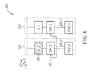
- FIG. 6 is a diagram illustrating an exemplary sensing cell according to a second embodiment of the present invention.
- the exemplary sensing cell 500 includes, but is not limited to, a first type sensing device 510 and a second type sensing device 520.
- the first type sensing device 510 includes the first sensor S_1 shown in FIG. 5 , a first pad PAD_1 , and a first switch SW_1.
- the sensing cell 500 receives an input event I_E
- the first sensor S_1 is arranged to generate a first type sensing signal SS_1 according to the input event I_E.
- the first switch SW_1 is arranged for controlling the first sensor S_1 to transmit the first type sensing signal SS_1 to the first pad PAD_1 according to a control signal SC.
- the second type sensing device 520 includes the second sensor S_2 and the obstruction unit SD shown in FIG. 5 , and further includes a second pad PAD_2, and a second switch SW_2.
- the obstruction unit SD is arranged to obstruct an input signal of the input event I_E from being transmitted to the second sensor S_2 (e.g., obstructing the path used by the second sensor S_2 to receive the input signal) when the sensing cell 500 receives the input event I_E.
- the second sensor S_2 generates a second type sensing signal SS_2 without receiving the input signal of the input event I_E.
- the second switch SW_2 is arranged to control the second sensor S_2 to transmit the second type sensing signal SS_2 to the second pad PAD_2 according to the control signal SC.
- the sensing cell 500 may output the first type sensing signal SS_1 and the second type sensing signal SS_2 simultaneously.
- each sensing device included in the sensing cell 500 further includes a switch and a pad, wherein the switch is arranged to control the transmission of the sensing signal of the sensing device, and the pad is arranged to receive the sensing signal of the sensing device.
- the first switch SW_1 and the second switch SW_2 may be implemented by transistors, and the first sensor S_1 and the second sensor S_2 may be implemented by photo-sensing devices.
- the sensing cell 500 may thus be applied to in-cell photo-sensing system 100 shown in FIG. 1 .
- the second type sensing device shown in FIG. 5 / FIG. 6 may also achieve the objective of generating the second sensing signal SS_2 not according to the input event I_E.
- the obstruction unit SD may be substituted by an attenuation unit.
- the sensors shown in FIG. 6 may not be coupled to the switches and/or the pads shown in FIG. 6 .
- the first type sensing device 510 may omit the pad PAD_1 (i.e., outputting the first type sensing signal SS_1 directly), and the second type sensing device 520 may omit the pad PAD_2 (i.e., outputting the second type sensing signal SS_2 directly).
- the second type sensing device 520 may omit the obstruction unit SD, and the second sensor S_2 may have a design (e.g., the inner material and/or the architecture design) different from that of the first sensor S_1, which realizes the sensing ability thereof to detect the input event I_E is different from the sensing ability of the first type sensing device 510 to detect the input event I_E.
- the first type sensing device 510 may omit the pad PAD_1 (i.e., outputting the first type sensing signal SS_1 directly), the second type sensing device 520 may omit the obstruction unit SD and the pad PAD_2 (i.e., outputting the second type sensing signal SS_2 directly), and the second sensor S_2 may have a design (e.g., the inner material and/or the architecture design) different from that of the first sensor S_1.
- the sensing cell architecture shown in FIG. 4 may be applied to other types of sensing systems (e.g., a thermal sensing system).
- FIG. 7 is a diagram illustrating a generalized sensing apparatus for sensing a touch position on a display panel according to an embodiment of the present invention.
- the sensing apparatus 600 includes a sensing cell 602 and a processing circuit 604.
- the sensing cell is disposed inside the display panel, and includes a first type sensing device 610 and a second type sensing device 620.
- the first type sensing device 610 is arranged to generate a first type sensing signal SS_1 when the sensing cell 602 receives an input event I_E.
- the second type sensing device 620 is adjacent to the first type sensing device 610, and arranged to generate a second type sensing signal SS_2 when the sensing cell 602 receives the input event I_E, wherein a sensing ability of the first type sensing device 610 to detect the input event I_E is different from a sensing ability of the second type sensing device 620 to detect the input event I_E.
- the processing circuit 604 is coupled to the sensing cell 602, and arranged to output a sensing output signal S_OUT corresponding to the sensing cell 602 according to a difference between the first type sensing signal SS_1 and the second type sensing signal SS_2.
- the exemplary implementations of the sensing cells 300-500 shown in FIGs.3-5 may be employed to implement the different sensing abilities to the input event I_E between the first type sensing device 610 and the second type sensing device 620.
- the first type sensing device 610 may correspond to the first type sensing device 310 shown in FIG. 4
- the second type sensing device 620 may correspond to the second type sensing device 320 shown in FIG. 4 . Therefore, in implementations where the sensing cell 602 employs the architectures of the sensing cells 300-500 shown in FIGs.3-5 , further description is omitted here for brevity. However, this is for illustrative purposes only, and is not meant to be a limitation of the present invention. In other words, any implementation, which employs sensing devices with different sensing abilities to generate a differential sensing output according to individual sensing signals generated due to the same input event, also obeys the spirit of the present invention and falls within the scope of the present invention.
- FIG. 8 is a diagram illustrating an exemplary sensing apparatus for sensing a touch position on a display panel according to an embodiment of the present invention.
- the exemplary sensing apparatus 606 may be used to replace the in-cell photo-sensing system 100 shown in FIG. 1 , and includes a plurality of photo-sensing cells 602_1-602_n and a processing circuit 608.
- the photo-sensing cells 602_1-602_n include a plurality of photo-sensing devices (e.g., in-cell photo sensors) PD1_1 -PD1_n and PD2_1-PD2_n, a plurality of obstruction units SD_1-SD_n, a plurality of transistors M1_1-M1_n and M2_1-M2_n, and a plurality of pads PAD1_1-PAD1_n and PAD2_1-PAD2_n, respectively.
- a plurality of photo-sensing devices e.g., in-cell photo sensors
- PD1_1 -PD1_n and PD2_1-PD2_n e.g., in-cell photo sensors
- a plurality of obstruction units SD_1-SD_n e.g., in-cell photo sensors
- transistors M1_1-M1_n and M2_1-M2_n e.g.,
- a first type sensing device includes the photo-sensing device PD1_1, the transistor M1_1, and the pad PAD1_1
- a second type sensing device includes the photo-sensing device PD2_1, the obstruction unit SD_1, the transistor M2_1, and the pad PAD2_1, wherein the transistor M1_1 and M2_1 are conducted according to a control signal SC.
- the second type sensing device may omit the obstruction unit SD_1, and the photo-sensing device PD2_1 may have a design (e.g., the inner material and/or the architecture design) different from that of the photo-sensing device PD1_1, which realizes that the sensing ability of the second type sensing device to detect the input event I_E is different from the sensing ability of the first type sensing device to detect the input event I_E.
- the sensing apparatus 606 may be employed to improve the touch event detection quality of the in-cell photo-sensing system 100 shown in FIG. 1 after reading above paragraphs directed to FIGs. 3-6A , further description is omitted here for brevity.
- a first type sensing signal and a second type sensing signal of a sensing cell may be transmitted to a processing circuit first, then the processing circuit may generate a sensing output signal according to a difference between the first type sensing signal and the second type sensing signal, and the sensing output signal may be transmitted to a readout circuit of the backend circuit.
- FIG. 9 is a diagram illustrating another exemplary sensing apparatus for sensing a touch position on a display panel according to another embodiment of the present invention. As shown in FIG.
- the architecture of the exemplary sensing apparatus 616 is based on the architecture of the exemplary sensing apparatus 606 shown in FIG. 8 , and the major difference therebetween is that a first type sensing signal and a second sensing signal corresponding to each of the sensing cells 612_1-612_n (e.g., the first type sensing signal SS_1 and the second sensing signal SS_2 corresponding to the sensing cell 612_1) may be transmitted to the processing circuit 618 directly for generating corresponding sensing output signals S_OUT1-S_OUT_n, respectively.
- a first type sensing signal and a second sensing signal corresponding to each of the sensing cells 612_1-612_n e.g., the first type sensing signal SS_1 and the second sensing signal SS_2 corresponding to the sensing cell 612_1
- the processing circuit 618 may transmit the sensing output signals S_OUT1-S_OUT_n to the corresponding pads PAD_1-PAD_n for a readout circuit of the backend circuit (not shown in FIG. 9 ) to perform further processing.
- the sensing apparatus 616 may save half the number of pads.
- the above processing circuit outputs the sensing output signal according to a difference between the received first type sensing signal and the received second type sensing signal of each the sensing cell, which reduces the effects caused by the process variation and the circuit noise interference, and an illumination event (i.e., the input event I_E) may thus be detected more accurately.
- the sensing cell 602 may also realize the sufficient difference in sensing abilities between the above two sensing devices by adjusting the material and/or the architecture of one of the first type sensing device 610 and the second type sensing device 620.
- the second type sensing device 620 is configured with the material of low transparency, resulting in a sufficient difference in received light intensities between the first type sensing device 610 and the second type sensing device 620. Therefore, there is a sufficient difference between the first type sensing signal SS_1 and the second type sensing signal SS_2 for the processing circuit 604 to detect an illumination event.
- a first type sensing signal SS_1 of the sensing cell 602_1 may be regarded as including a photocurrent signal S_PC and a noise signal S_N1, wherein the noise signal S_N1 includes a common mode noise signal S_NCM1 (resulting from the local factor of the process variation and the noise coupling) and a differential mode noise S_NDF1 (resulting from the random factor of the process variation and the noise coupling).
- the second type sensing signal SS_2 may also be regarded as including a dark-current signal S_DC and a noise signal S_N2, wherein the noise signal S_N2 includes a common mode noise signal S_NCM2 and a differential mode noise S_NDF2.
- the processing circuit 608 directly outputs a difference between the first type sensing signal SS_1 and the second type sensing signal SS_2 as the sensing output signal S_OUT1 corresponding to the sensing cell 602_1.
- the first type sensing device and second type sensing device of the sensing cell 602_1 are adjacent to each other, the first type sensing device and second type sensing device of the sensing cell 602_1 may be regarded as being affected by the same local factor of the process variation and the noise coupling. That is, the signal S_OUT12 may be regarded as zero. In addition, regarding the signal S_OUT11, the signal S_OUT13 is negligible.
- the sensing apparatus 606 successfully reduces the effects caused by the process variation and the noise coupling on detecting the input event I_E, and the SNR of the sensing apparatus 606 is greatly enhanced.
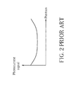
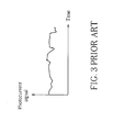
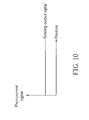
- FIG. 10 is a diagram illustrating the relation between the photocurrent signal intensity and the position on a display panel of the sensing apparatus 606 shown in FIG. 8
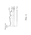
- FIG. 11 is a diagram illustrating the relation between the photocurrent signal intensity and the time in the sensing cell 602_1 shown in FIG. 8 .
- a first type sensing signal corresponding to a photocurrent signal
- a second type sensing signal corresponding to a dark-current signal
- a difference SS_D between the first type sensing signal SS_1 and the second type sensing signal SS_2 is of a sufficient amount and a stable signal value, which means that the noise coupling generated between adjacent sensing cells are greatly reduced.
- the in-cell photo-sensing system 100 shown in FIG. 1 as the sensing ability of the photo-sensing device PD_1 to detect the input event I_E is the same as the sensing ability of the photo-sensing device PD_2 to detect the input event I_E, the in-cell photo-sensing system 100 may fail to realize the differential sensing output. In other words, if the in-cell photo-sensing system 100 shown in FIG.
- the photocurrent PI_2 may correspond to the sensing signal SS_1 shown in FIG. 11
- the photocurrent PI_1 may correspond to the sensing signal SS_3 shown in FIG. 11 .
- the wanted signal can not be extracted.
- the aforementioned first type sensing device and second type sensing signal may have a plurality of arrangements on the circuit layout.
- the sensing cells included in the sensing apparatus 606 are arranged in array on a display panel
- the photo-sensing devices PD1 and PD_2 (corresponding to the first type sensing device and the second type sensing device, respectively) included in the sensing cell 602_1 may not be arranged in the same column or the same row.
- circuit layouts of the first type sensing devices and the second type sensing devices may employ the common-centroid layout technique.
- the proposed sensing apparatus may greatly reduce the effects caused by the processing variation and/or the noise coupling when detecting the input event, and the SNR of the sensing apparatus is also enhanced.
Landscapes
- Engineering & Computer Science (AREA)
- General Engineering & Computer Science (AREA)
- Theoretical Computer Science (AREA)
- Human Computer Interaction (AREA)
- Physics & Mathematics (AREA)
- General Physics & Mathematics (AREA)
- Position Input By Displaying (AREA)
- Electronic Switches (AREA)
- User Interface Of Digital Computer (AREA)
Applications Claiming Priority (1)
| Application Number | Priority Date | Filing Date | Title |
|---|---|---|---|
| US201161477601P | 2011-04-20 | 2011-04-20 |
Publications (3)
| Publication Number | Publication Date |
|---|---|
| EP2515214A2 true EP2515214A2 (de) | 2012-10-24 |
| EP2515214A8 EP2515214A8 (de) | 2012-11-28 |
| EP2515214A3 EP2515214A3 (de) | 2016-05-25 |
Family
ID=46087417
Family Applications (1)
| Application Number | Title | Priority Date | Filing Date |
|---|---|---|---|
| EP12002667.9A Withdrawn EP2515214A3 (de) | 2011-04-20 | 2012-04-17 | Messvorrichtung und Messverfahren zum Messen der Berührungsposition auf der Anzeigetafel |
Country Status (5)
| Country | Link |
|---|---|
| US (1) | US20120268425A1 (de) |
| EP (1) | EP2515214A3 (de) |
| JP (2) | JP2012227925A (de) |
| CN (1) | CN102750045A (de) |
| TW (1) | TWI459265B (de) |
Families Citing this family (2)
| Publication number | Priority date | Publication date | Assignee | Title |
|---|---|---|---|---|
| US20180146149A1 (en) | 2016-11-21 | 2018-05-24 | Samsung Electronics Co., Ltd. | Event-based sensor, user device including the same, and operation method of the same |
| KR102656177B1 (ko) | 2019-02-11 | 2024-04-12 | 삼성전자주식회사 | 신호를 축적하기 위한 센서 |
Family Cites Families (26)
| Publication number | Priority date | Publication date | Assignee | Title |
|---|---|---|---|---|
| JPS61167824A (ja) * | 1985-01-18 | 1986-07-29 | Nippon Soken Inc | 光電変換回路 |
| JPS6334821A (ja) * | 1986-07-29 | 1988-02-15 | 松下電器産業株式会社 | 磁性体検出装置 |
| JPS63133128A (ja) * | 1986-11-26 | 1988-06-04 | Canon Inc | 光差分センサ |
| JPH01305328A (ja) * | 1988-06-02 | 1989-12-08 | Fuji Electric Co Ltd | 光強度検出回路 |
| JPH0798628A (ja) * | 1993-09-29 | 1995-04-11 | Hitachi Seiko Ltd | ワイヤレス座標読取装置 |
| JP2001217318A (ja) * | 2000-02-01 | 2001-08-10 | Fuji Electric Co Ltd | 半導体装置 |
| JP4599985B2 (ja) * | 2004-10-21 | 2010-12-15 | セイコーエプソン株式会社 | 光検出回路、電気光学装置、および電子機器 |
| JP4533259B2 (ja) * | 2005-06-29 | 2010-09-01 | アルプス電気株式会社 | 入力装置 |
| JP2007094098A (ja) * | 2005-09-29 | 2007-04-12 | Sanyo Epson Imaging Devices Corp | 液晶表示装置及び電子機器 |
| JP2007310628A (ja) * | 2006-05-18 | 2007-11-29 | Hitachi Displays Ltd | 画像表示装置 |
| JP4735575B2 (ja) * | 2007-03-16 | 2011-07-27 | ソニー株式会社 | 表示装置 |
| JP2008281615A (ja) * | 2007-05-08 | 2008-11-20 | Seiko Epson Corp | 電気光学装置及びその製造方法、電子機器 |
| JP5315910B2 (ja) * | 2007-10-12 | 2013-10-16 | ソニー株式会社 | 接触センサ |
| JP2009128686A (ja) * | 2007-11-26 | 2009-06-11 | Sony Corp | 表示装置および電子機器 |
| JP5239317B2 (ja) * | 2007-11-30 | 2013-07-17 | セイコーエプソン株式会社 | 液晶装置及び電子機器 |
| EP2073055A1 (de) * | 2007-12-20 | 2009-06-24 | TPO Displays Corp. | Detektion einer Auflichtverteilung |
| JP2009265512A (ja) * | 2008-04-28 | 2009-11-12 | Sony Corp | 液晶表示装置 |
| JP5333964B2 (ja) * | 2008-06-27 | 2013-11-06 | 株式会社ジャパンディスプレイ | 光検出装置、電気光学装置及び電子機器 |
| JP2010020674A (ja) * | 2008-07-14 | 2010-01-28 | Tokai Rika Co Ltd | タッチセンサ装置 |
| US8614690B2 (en) * | 2008-09-26 | 2013-12-24 | Apple Inc. | Touch sensor panel using dummy ground conductors |
| TWI402738B (zh) * | 2009-05-27 | 2013-07-21 | Wintek Corp | 觸控裝置以及觸控感測方法 |
| JP2010286314A (ja) * | 2009-06-10 | 2010-12-24 | Act Lsi:Kk | 薄型で耐ノイズ性にすぐれた静電式近接センサの電極システム、および静電式近接センサ |
| US8519984B2 (en) * | 2009-08-20 | 2013-08-27 | Acer Incorporated | Input device and display system having the same |
| JP2011065133A (ja) * | 2009-08-20 | 2011-03-31 | Toppan Printing Co Ltd | 液晶表示装置、ブラックマトリクス基板、及びカラーフィルタ基板 |
| TW201115420A (en) * | 2009-10-29 | 2011-05-01 | Ideacom Technology Corp | Touch panel detecting apparatus and the method therefor |
| KR101588355B1 (ko) * | 2009-12-23 | 2016-02-15 | 삼성디스플레이 주식회사 | 터치스크린 기판, 이의 제조 방법 및 표시 패널 |
-
2012
- 2012-01-31 TW TW101103041A patent/TWI459265B/zh not_active IP Right Cessation
- 2012-02-14 CN CN2012100325470A patent/CN102750045A/zh active Pending
- 2012-04-05 JP JP2012086274A patent/JP2012227925A/ja active Pending
- 2012-04-15 US US13/447,274 patent/US20120268425A1/en not_active Abandoned
- 2012-04-17 EP EP12002667.9A patent/EP2515214A3/de not_active Withdrawn
-
2015
- 2015-05-29 JP JP2015109245A patent/JP2015215904A/ja active Pending
Non-Patent Citations (1)
| Title |
|---|
| None |
Also Published As
| Publication number | Publication date |
|---|---|
| EP2515214A8 (de) | 2012-11-28 |
| EP2515214A3 (de) | 2016-05-25 |
| TWI459265B (zh) | 2014-11-01 |
| CN102750045A (zh) | 2012-10-24 |
| TW201243675A (en) | 2012-11-01 |
| US20120268425A1 (en) | 2012-10-25 |
| JP2012227925A (ja) | 2012-11-15 |
| JP2015215904A (ja) | 2015-12-03 |
Similar Documents
| Publication | Publication Date | Title |
|---|---|---|
| CN108121477B (zh) | 触摸感测电路、触摸显示装置及触摸感测方法 | |
| KR101459776B1 (ko) | 액정 장치 | |
| KR101799523B1 (ko) | 리모트 센싱과 터치 센싱이 가능한 광터치 스크린 장치 | |
| CN101359111B (zh) | 液晶装置 | |
| US9575611B2 (en) | Touch panel | |
| TWI488091B (zh) | 光學式觸控顯示面板 | |
| US9287315B2 (en) | Thin film transistor array substrate for digital photo-detector | |
| US9269740B2 (en) | Thin film transistor array substrate for digital photo-detector | |
| US9268447B2 (en) | Touch display panel, touch display device and driving method thereof | |
| JP5364934B2 (ja) | タッチシステム及び認識方法 | |
| EP1903788B1 (de) | Photodetektoranordnung | |
| WO2009110293A1 (ja) | 光センサ付き表示装置 | |
| KR20130028581A (ko) | 광센싱 장치 및 그 구동 방법, 광센싱 장치를 포함하는 광터치 스크린 장치 | |
| CN106406617A (zh) | 触控面板及其触控检测方法以及显示装置 | |
| US8525953B2 (en) | Display device | |
| WO2014206030A1 (zh) | 一种触控驱动电路、光学式内嵌触摸屏及显示装置 | |
| TW200609812A (en) | Optical position sensing device including interlaced groups of photosensitive elements | |
| US9069412B2 (en) | Touch-sensor-equipped display device comrpising photodetecting elements | |
| CN113705319A (zh) | 光学指纹感测装置以及光学指纹感测方法 | |
| CN105302286A (zh) | 光感测装置及安排感光组件的方法 | |
| JP5008031B2 (ja) | 液晶装置および電子機器 | |
| EP2515214A2 (de) | Messvorrichtung und Sendeverfahren zum Messen der Berührungsposition auf der Anzeigetafel | |
| EP2485124A1 (de) | Anzeigevorrichtung | |
| CN103645821A (zh) | 触控模块的感光像素电路 | |
| TW201415307A (zh) | 觸碰感測系統 |
Legal Events
| Date | Code | Title | Description |
|---|---|---|---|
| PUAI | Public reference made under article 153(3) epc to a published international application that has entered the european phase |
Free format text: ORIGINAL CODE: 0009012 |
|
| AK | Designated contracting states |
Kind code of ref document: A2 Designated state(s): AL AT BE BG CH CY CZ DE DK EE ES FI FR GB GR HR HU IE IS IT LI LT LU LV MC MK MT NL NO PL PT RO RS SE SI SK SM TR |
|
| AX | Request for extension of the european patent |
Extension state: BA ME |
|
| RIN1 | Information on inventor provided before grant (corrected) |
Inventor name: HAN, CHEN-HSEIN Inventor name: LIAW, SHEN-TAI Inventor name: YUAN, CHIH-MING Inventor name: HWANG, NAEJYE |
|
| PUAL | Search report despatched |
Free format text: ORIGINAL CODE: 0009013 |
|
| RIC1 | Information provided on ipc code assigned before grant |
Ipc: G06F 3/041 20060101AFI20160413BHEP Ipc: G06F 3/042 20060101ALI20160413BHEP |
|
| AK | Designated contracting states |
Kind code of ref document: A3 Designated state(s): AL AT BE BG CH CY CZ DE DK EE ES FI FR GB GR HR HU IE IS IT LI LT LU LV MC MK MT NL NO PL PT RO RS SE SI SK SM TR |
|
| AX | Request for extension of the european patent |
Extension state: BA ME |
|
| RIC1 | Information provided on ipc code assigned before grant |
Ipc: G06F 3/041 20060101AFI20160420BHEP Ipc: G06F 3/042 20060101ALI20160420BHEP |
|
| STAA | Information on the status of an ep patent application or granted ep patent |
Free format text: STATUS: THE APPLICATION IS DEEMED TO BE WITHDRAWN |
|
| 18D | Application deemed to be withdrawn |
Effective date: 20161101 |