EP2073055A1 - Detektion einer Auflichtverteilung - Google Patents
Detektion einer Auflichtverteilung Download PDFInfo
- Publication number
- EP2073055A1 EP2073055A1 EP08165314A EP08165314A EP2073055A1 EP 2073055 A1 EP2073055 A1 EP 2073055A1 EP 08165314 A EP08165314 A EP 08165314A EP 08165314 A EP08165314 A EP 08165314A EP 2073055 A1 EP2073055 A1 EP 2073055A1
- Authority
- EP
- European Patent Office
- Prior art keywords
- light
- shadow
- array
- incident light
- distribution
- Prior art date
- Legal status (The legal status is an assumption and is not a legal conclusion. Google has not performed a legal analysis and makes no representation as to the accuracy of the status listed.)
- Withdrawn
Links
Images


Classifications
-
- G—PHYSICS
- G02—OPTICS
- G02F—OPTICAL DEVICES OR ARRANGEMENTS FOR THE CONTROL OF LIGHT BY MODIFICATION OF THE OPTICAL PROPERTIES OF THE MEDIA OF THE ELEMENTS INVOLVED THEREIN; NON-LINEAR OPTICS; FREQUENCY-CHANGING OF LIGHT; OPTICAL LOGIC ELEMENTS; OPTICAL ANALOGUE/DIGITAL CONVERTERS
- G02F1/00—Devices or arrangements for the control of the intensity, colour, phase, polarisation or direction of light arriving from an independent light source, e.g. switching, gating or modulating; Non-linear optics
- G02F1/01—Devices or arrangements for the control of the intensity, colour, phase, polarisation or direction of light arriving from an independent light source, e.g. switching, gating or modulating; Non-linear optics for the control of the intensity, phase, polarisation or colour
- G02F1/13—Devices or arrangements for the control of the intensity, colour, phase, polarisation or direction of light arriving from an independent light source, e.g. switching, gating or modulating; Non-linear optics for the control of the intensity, phase, polarisation or colour based on liquid crystals, e.g. single liquid crystal display cells
- G02F1/133—Constructional arrangements; Operation of liquid crystal cells; Circuit arrangements
- G02F1/1333—Constructional arrangements; Manufacturing methods
- G02F1/13338—Input devices, e.g. touch panels
-
- G—PHYSICS
- G01—MEASURING; TESTING
- G01S—RADIO DIRECTION-FINDING; RADIO NAVIGATION; DETERMINING DISTANCE OR VELOCITY BY USE OF RADIO WAVES; LOCATING OR PRESENCE-DETECTING BY USE OF THE REFLECTION OR RERADIATION OF RADIO WAVES; ANALOGOUS ARRANGEMENTS USING OTHER WAVES
- G01S3/00—Direction-finders for determining the direction from which infrasonic, sonic, ultrasonic, or electromagnetic waves, or particle emission, not having a directional significance, are being received
- G01S3/78—Direction-finders for determining the direction from which infrasonic, sonic, ultrasonic, or electromagnetic waves, or particle emission, not having a directional significance, are being received using electromagnetic waves other than radio waves
- G01S3/782—Systems for determining direction or deviation from predetermined direction
-
- G—PHYSICS
- G06—COMPUTING; CALCULATING OR COUNTING
- G06F—ELECTRIC DIGITAL DATA PROCESSING
- G06F3/00—Input arrangements for transferring data to be processed into a form capable of being handled by the computer; Output arrangements for transferring data from processing unit to output unit, e.g. interface arrangements
- G06F3/01—Input arrangements or combined input and output arrangements for interaction between user and computer
- G06F3/03—Arrangements for converting the position or the displacement of a member into a coded form
- G06F3/041—Digitisers, e.g. for touch screens or touch pads, characterised by the transducing means
- G06F3/042—Digitisers, e.g. for touch screens or touch pads, characterised by the transducing means by opto-electronic means
Definitions
- This invention relates to the detection of the characteristics of an incident light distribution, particularly but not exclusively for use with display devices including a touch input.
- touch-screen technologies are well-known and widely used. They include so-called 'resistive' and 'capacitive' technologies. Most such technologies however add significant cost and complexity to a display module, and impair front-of-screen performance.
- the user's finger makes contact with the top surface of the display device, whereas the sensor circuitry is most preferably integrated into the active plate of the display.
- the spacing between the active plate and the surface of the display means that a point of contact cannot be derived unambiguously from a shadow cast. This problem is compounded if there is more than one directional light source.
- a device for detecting an incident light distribution comprising:
- This arrangement uses a shadow cast from an element of known shape and position in order to derive information about the incident light.
- the processor can also be adapted to derive information relating to the colour distribution of the incident light.
- the processor is adapted to derive a representation of the incident light as originating from one or more light sources in different positions.
- the information derived can be used in a lighting device in which a light output device is controlled in dependence on the information relating to the directional distribution of the incident light. This can be used to generate lighting effects which are dependent on the ambient light properties.
- the shadow analysis can instead be used to interpret shadows of elements of unknown shape or position.
- the information derived can be used in a shadow detection system, in which a second array of light sensors is provided for detecting a shadow cast by a user of the device.
- a processor is provided for interpreting the shadow cast by the user of the device, which uses the information relating to the directional distribution of the incident light.
- This shadow detection system can be used in a display device with a touch input, in which the display device further comprises an array of display pixels.
- This arrangement improves the accuracy of a simple light sensing touch input system.
- the system can be implemented with low cost, and may for example be used for a coarse resolution touch sensitive input system.
- the array of display pixels comprises an array of pixel circuits, wherein the second array of light sensors is integrated with the pixel circuits.
- This provides low cost integration of the light sensor array into the display active plate, which carries the pixel circuits.
- the display device preferably comprises a liquid crystal display.
- the shadow casting element can be arranged outside the display output area, so that the light modelling function does not disturb the display output, but is nearby so that the light at the touch input of the display device is represented by the modelling.
- the shadow casting element can be arranged at the edges and/or corners of the display output area.
- the invention also provides a method of detecting an incident light distribution, comprising:
- This method can be part of a method of providing a light output, in which a light output device is controlled in dependence on the information relating to the directional distribution of the incident light.
- the method can be part of a method of interpreting a touch input to a touch input device, in which a shadow cast by a user of the device is detected and interpreted using the information relating to the directional distribution of the incident light.
- the invention provides detection and analysis of a light distribution so that shadows cast or light scattering can be interpreted.
- the invention uses a shadow cast from an element of known shape and position in order to derive information about the incident light. This in turn can be used to provide desired lighting effects, or to interpret shadows of elements of unknown shape or position in a touch sensor device.
- the invention uses known light sensing technology to implement a touch sensing function.
- this approach has only recently been considered, the use of integrated light sensors is well known, for example for detecting ambient light levels, the ambient light level in turn being used for backlight control.
- Liquid crystal displays typically comprise an active plate and a passive plate between which liquid crystal material is sandwiched.
- the active plate comprises an array of transistor switching devices, typically with one transistor associated with each pixel of the display.
- Each pixel is also associated with a pixel electrode on the active plate to which a signal is applied for controlling the brightness of the individual pixel.
- Light sensors can be formed as part of the active plate using thin film technology, and this is a convenient way of adding the light sensor capability without requiring additional process steps or separate components.
- the light sensitive devices may for example be thin film transistors, thin film diodes, lateral diodes or light sensitive resistors or other photosensitive devices.
- Figure 1 shows in a simplified form the way in which the light sensors can be integrated within the display.
- the display is formed from two glass substrates 24,26 with a liquid crystal layer 28 between them.
- a light sensor 30 is fabricated on the lower substrate 26 which is closest to the backlight 42 (or backlight light guide) of the display. Ambient light from the front of the display is able to pass through the upper substrate 24 and the liquid crystal layer 28 to reach the light sensor 30.
- the sensor can also receive ambient light which has passed through the display and has been modulated by the display pixels as indicated by the example light path 31.
- the sensor may also receive light from the backlight of the display as indicated by light paths 32 and 34, and which has passed through the lower substrate 26.
- the contributions to the output signal from the modulated ambient light and from the backlight are undesirable and should be minimised and ideally eliminated.
- An alternative approach is to use a pulsed backlight (for example at 60Hz), and to make the ambient light measurements during the "off" periods of the backlight. Of course, this does not allow the backlight to be driven to a continuous maximum brightness output.
- Figure 1 shows a light masking layer 36.
- the use of a black mask layer is well known to shield the areas of the active plate through which unmodulated light can pass, and to shield the transistors as their operating characteristics are light-dependent.
- the top and bottom polarisers 38, 40 are also shown.
- the black mask layer has an opening to allow ambient light to reach the sensors 30.
- the light sensors can be integrated within the display pixels so that light sensing can be implemented across the display area.
- One way to achieve this is to introduce a second sensor which has a different sensitivity to the ambient light level but a similar sensitivity to the unwanted components of light.
- the sensor arrangement 30 comprises a first sensor A which is exposed to the ambient illumination, while a second sensor B is covered by the light masking layer 36 (in this example shown beneath the liquid crystal layer rather than on top as in Figure 1 ) so that its output contains a much lower contribution from the ambient light when compared to sensor
- the sensors A and B have the same area, a subtraction of the light sensed by sensor B from the light sensed by sensor A gives the ambient light level.
- Sensor B is illuminated only by light which has reached the sensor from the backlight, whereas as sensor A is illuminated by the ambient light as well as light which has reached the sensor from the backlight.
- the use of two sensors thus enables processing of the signals received so that a more accurate determination of the incoming (ambient) light level can be obtained.
- Sensor B has the same area as sensor A but is divided into two equal parts, B1 and B2, which are located on either side of sensor A.
- the preferred examples of the invention use this type of light sensing capability to implement a touch sensitive input. Furthermore, the accuracy of interpretation of shadows is improved, by using a light modelling arrangement.
- Figure 3 shows the concept underlying the invention, for determining the nature, in particular the directional distribution, of the light incident on a device.
- the ambient light is represented schematically as a light source 50.
- a shadow casting element 52 is provided in the path between the light source 50 and the active plate, which carries an array 54 of light sensors.
- the array of sensors 54 is used to characterise the ambient light, and is spaced a known distance behind the known shadow casting element 52.
- Figure 3 shows a simple system of generating and measuring a reference shadow for the illumination environment.
- This reference shadow can then be used to significantly aid the interpretation of shadows of unknown bodies (i.e. the user finger or stylus) in front of the screen, and thus increase reliability/robustness of interpreting shadow images to enable a touch input interface.
- the direction of the illumination being shadowed, or the directional distribution of the illumination being shadowed allows more accurate interpretation of shadow maps.
- the reference shadow from the known shadow casting element indicates that the general direction of illumination is at a certain angle to the normal, then this information can be used to interpret a cast shadow from an object, in particular to provide an accurate estimate of the position of the object.
- the shadow as well as the light conditions are processed to derive an accurate estimate of the position of the object which has cast the shadow.
- Figure 4 shows one possible implementation of the sensor array and shadow casting element.
- the same reference numerals are used for the same components as in Figure 2 , and the description is not repeated for the same components.
- the shadow casting element 52 is formed from the black mask layer 36, and the array of light sensors is formed on the active plate using the same technology and layers as the pixel circuits and the light sensors provided with the pixels. This provides a fully integrated solution.
- the spacing between the black mask layer 36 and the pixel circuits and sensors may not be large enough to provide the desired resolution of detection.
- the shadow casting element 52 can instead be provided further from the sensors, for example on top of the (thicker) glass plate 24.
- the separation between the shadow casting element and the light sensor array can include a glass substrate on which the display is fabricated.
- the light sensing elements of the array 54 will be of the same type and formed using the same process steps as the in-pixel light sensors, such as photodiodes or phototransistors.
- the processing implemented to model the light distribution can simply determine the centre of the shadow area, either as the darkest sensor area, or the centre of the darkened area, wherein the darkened area is determined by applying thresholds to identify the boundary of the shaded area.
- the position of this shadow area centre compared to the position of the centre of the shadow casting element, then enables an average effective lighting direction to be determined. This lighting direction can then be used to reverse process the shadow cast by a user in order to estimate the position on the touch input surface.
- the light sensor array 54 can however be used to derive more accurate information, for example it may model the light distribution as a number of point sources.
- the accuracy with which this modelling can be implemented will depend on the number of light sensors in the array 54. This can range from a small array (e.g. 10x10) to a much larger array (e.g. 100x100) with more complicated processing.
- anti-aliasing effects may be achieved by having a straight edge to the shadow casting element 52, which is skewed by one sensor-pixel-width along its length.
- a circular shadow-casting element will also provide these anti-aliasing effects.
- the shadow casting element 52 can also be inverted, so as to have a central transparent region with an opaque surround, rather than an opaque element with a transparent surround.
- a circular aperture can be provided in an opaque mask.
- the angular/spatial resolution of the image created through an aperture is increased as the distance between the aperture and the sensor array is increased.
- the interpretation of the light distribution requires only a low resolution, so that the sensor array can spaced with a distance of the order of one aperture diameter.
- an opaque shadow-casting element can be approximately 3 to 5 times the linear size of the spacing between the shadow-casting element 52 and the sensor array 54.
- An aperture shadow-casting element can be approximately the same linear size or smaller than the linear size of the spacing between the shadow-casting element and the sensor array.
- the shadow analysis from the shadow-casting element is not limited to simply providing an overall input light direction. Indeed, the analysis of the shadow can enable many different properties of the ambient lighting to be determined, in addition to a general direction of illumination.
- the following observations can assist in the interpretation of the shadow cast::
- the sensor array and analysis can be used to analyse (mathematically or algorithmically) the light-pool by "fitting" overlapping circles of light to the measured data from the sensor array.
- the centre point of the different circles is offset, and diameter variations can also be introduced, as well as edge-sharpness functions.
- an extended shadow for example cast by the full length of a stylus.
- the shadow cast by the stylus shaft may be almost as dense as under the stylus tip where the stylus/finger is touching the glass.
- the type of lighting effect which is detected can be used to assist in the location of the touch input, in a number of different ways.
- a software algorithm can seek small areas of high density shadow, with hard-edges at least part-way around. This is because in diffuse light, there will only be a dark shadow directly beneath the point of contact.
- the density of the shadow at the stylus tip may not be markedly greater than that in the extended tail from the stylus shaft, and the sharpness falloff may also be less pronounced.
- the light direction determined by the shadow sensor can be used to assist in the interpretation of the user input. For example, if the shadow-sensor indicates that the dominant light is coming from the user's left, for example, then this would provide an indication that the leftmost point of an extended shadow cast on the display will correspond to the user's intended point-of-interaction.
- the analysis of the shadow cast seeks to identify up to 4 or 5 separate lights sources.
- the analysis of the shadow image can comprise a full image acquisition of the angular size of the shadow with a high-resolution grid of sensor pixels, for example with a binary threshold applied to the pixel signals.
- analog light levels can also be used from the pixel sensors, so as to gauge the angular size of the light source, by measuring the "fuzziness" of the shadow.
- the examples above use the shadow sensor to model the light distribution and direction from one or more light sources.
- the sensor array may contain a mixture of sensors of differing colour-sensitivity so that the colour or colour distribution of the incident light can also be analysed.
- This mixture of colour sensors could be a Bayer colour filter mosaic (as used in CCD cameras), or else adjacent individual-colour sensor arrays could be used, each with their own shadow-forming elements, with each individual colour sensor array using a single overall colour filter.
- Characterisation of the distribution/directionality of ambient light may have other applications in lighting, for example ambient-light sensing/simulation/reconstruction, and so-called ambient intelligence (guessing the location/environment) in portable consumer electronics devices.
- Colour sensing as mentioned above may be used in such an application to detect, for example, the diffuse hemisphere of blue sky distinct from the near point source of the yellow-white sun.
- the invention in most general form relates to the detection/modelling of a light distribution for any purpose, not only for a touch input display device.
- the analysis of the ambient light distribution can be used to control a display output, for example to generate lighting effects which depend on the ambient lighting.
- Mood lighting is one example
- the re-simulation of outdoor ambient light conditions indoors is another example.
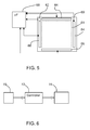
- Figure 5 shows schematically a first example of system that can use the light detection system and method of the invention, in the form of a display 60 having a shadow based touch sensitive input.
- the display 60 has an area 61 in which a pixel array is formed.
- the light detection system is shown as 62, outside the pixel area, and comprises a first array of light sensors.
- a second array of light sensors is provided in the area 61, for example with a light sensor integrated into each display pixel circuit.
- the display pixels are controlled by row and column driver circuits 64, and the light sensors are read by row and column readout circuits 66. These circuits are all under the control of the processor 68, which implements the light detection and modelling method explained above, as well as the interpretation of the touch input based on shadow detection within the second sensor array.
- Figure 6 is a second example of system that can use the light detection system and method of the invention, in the form of a controlled light output device.
- the light detection system is shown as 70, and the signals are provided to a lighting controller 72 which implements the light detection and modelling method explained above, and then controls a light output device 74 in dependence on the ambient light characteristics, as explained above.
Priority Applications (2)
| Application Number | Priority Date | Filing Date | Title |
|---|---|---|---|
| TW097149627A TWI372350B (en) | 2007-12-20 | 2008-12-19 | Image display systems and display device control methods |
| US12/340,240 US8154534B2 (en) | 2007-12-20 | 2008-12-19 | Detection of an incident light distribution |
Applications Claiming Priority (1)
| Application Number | Priority Date | Filing Date | Title |
|---|---|---|---|
| US1565807P | 2007-12-20 | 2007-12-20 |
Publications (1)
| Publication Number | Publication Date |
|---|---|
| EP2073055A1 true EP2073055A1 (de) | 2009-06-24 |
Family
ID=40342793
Family Applications (1)
| Application Number | Title | Priority Date | Filing Date |
|---|---|---|---|
| EP08165314A Withdrawn EP2073055A1 (de) | 2007-12-20 | 2008-09-26 | Detektion einer Auflichtverteilung |
Country Status (4)
| Country | Link |
|---|---|
| US (1) | US8154534B2 (de) |
| EP (1) | EP2073055A1 (de) |
| CN (1) | CN101477785A (de) |
| TW (1) | TWI372350B (de) |
Cited By (6)
| Publication number | Priority date | Publication date | Assignee | Title |
|---|---|---|---|---|
| EP2485126A1 (de) * | 2009-09-30 | 2012-08-08 | Sharp Kabushiki Kaisha | Anzeigevorrichtung |
| EP2485127A1 (de) * | 2009-09-30 | 2012-08-08 | Sharp Kabushiki Kaisha | Anzeigevorrichtung |
| EP2515214A3 (de) * | 2011-04-20 | 2016-05-25 | Integrated Digital Technologies, Inc. | Messvorrichtung und Messverfahren zum Messen der Berührungsposition auf der Anzeigetafel |
| US9733764B2 (en) | 2015-11-20 | 2017-08-15 | International Business Machines Corporation | Tracking of objects using pre-touch localization on a reflective surface |
| US9823782B2 (en) | 2015-11-20 | 2017-11-21 | International Business Machines Corporation | Pre-touch localization on a reflective surface |
| US10606468B2 (en) | 2015-11-20 | 2020-03-31 | International Business Machines Corporation | Dynamic image compensation for pre-touch localization on a reflective surface |
Families Citing this family (15)
| Publication number | Priority date | Publication date | Assignee | Title |
|---|---|---|---|---|
| US7809221B2 (en) * | 2007-05-02 | 2010-10-05 | Poa Sana Liquidating Trust | Shadow detection in optical touch sensor through the linear combination of optical beams and grey-scale determination of detected shadow edges |
| EP2282254A1 (de) * | 2008-05-12 | 2011-02-09 | Sharp Kabushiki Kaisha | Anzeigevorrichtung und steuerverfahren dafür |
| GB2460090A (en) * | 2008-05-16 | 2009-11-18 | Sony Corp | Ambient light detection device |
| KR100976527B1 (ko) * | 2008-10-14 | 2010-08-17 | 하이디스 테크놀로지 주식회사 | 광도전체를 이용한 터치스크린 기능이 내장된 액정표시장치 |
| JP5275956B2 (ja) * | 2009-10-15 | 2013-08-28 | 株式会社ジャパンディスプレイウェスト | 情報入力装置、情報入力プログラムおよび電子機器 |
| CN102221954B (zh) * | 2010-04-15 | 2014-01-29 | 中国移动通信集团公司 | 缩放显示装置、包括该装置的电子设备和缩放显示方法 |
| TWI409679B (zh) * | 2010-06-04 | 2013-09-21 | Au Optronics Corp | 光學式觸控面板及觸控顯示裝置及其觸控輸入方法 |
| TWI452550B (zh) * | 2010-07-23 | 2014-09-11 | Pixart Imaging Inc | 顯示面板及其組裝方法 |
| CN101976153A (zh) * | 2010-07-27 | 2011-02-16 | 苏州瀚瑞微电子有限公司 | 光敏触控系统 |
| US8786730B2 (en) | 2011-08-18 | 2014-07-22 | Microsoft Corporation | Image exposure using exclusion regions |
| FR2999771A1 (fr) * | 2012-12-18 | 2014-06-20 | St Microelectronics Grenoble 2 | Circuit et procede de mesure de niveau de luminosite ambiante |
| KR20180061482A (ko) * | 2016-11-28 | 2018-06-08 | 삼성디스플레이 주식회사 | 표시장치 |
| US10267889B1 (en) * | 2017-11-15 | 2019-04-23 | Avalex Technologies Corporation | Laser source location system |
| CN110265453B (zh) * | 2019-06-25 | 2021-11-12 | 京东方科技集团股份有限公司 | 显示面板、显示装置及显示控制方法 |
| US11132832B2 (en) * | 2019-08-29 | 2021-09-28 | Sony Interactive Entertainment Inc. | Augmented reality (AR) mat with light, touch sensing mat with infrared trackable surface |
Citations (5)
| Publication number | Priority date | Publication date | Assignee | Title |
|---|---|---|---|---|
| GB1567419A (en) * | 1977-12-20 | 1980-05-14 | Standard Telephones Cables Ltd | Sensors for heliostats |
| DE4410078A1 (de) * | 1993-03-23 | 1994-09-29 | Wacom Co Ltd | Optische Positionserfassungseinheit und optische Koordinateneingabeeinheit |
| DE19748826C1 (de) * | 1997-11-05 | 1999-02-11 | Kostal Leopold Gmbh & Co Kg | Sonnenstandsdetektor |
| GB2337170A (en) * | 1980-09-09 | 1999-11-10 | Marconi Co Ltd | Electromagnetic direction-finders |
| US20050200293A1 (en) * | 2004-02-24 | 2005-09-15 | Naugler W. E.Jr. | Penlight and touch screen data input system and method for flat panel displays |
Family Cites Families (14)
| Publication number | Priority date | Publication date | Assignee | Title |
|---|---|---|---|---|
| US4149197A (en) | 1977-10-11 | 1979-04-10 | Northern Telecom Limited | Direct imaging apparatus for an electronic document transmitter utilizing a linear array of photo-detectors |
| US4449084A (en) | 1981-12-28 | 1984-05-15 | University Of Pittsburgh | Positioning servo-mechanism or tachometer employing self-scanning light sensing array |
| US4577099A (en) | 1984-06-29 | 1986-03-18 | International Business Machines Corporation | Apparatus for proximity detection of an opaque pattern on a translucent substrate |
| US5428215A (en) | 1994-05-27 | 1995-06-27 | Her Majesty The Queen In Right Of Canada, As Represented By Minister Of National Defence Of Her Majesty's Canadian Government | Digital high angular resolution laser irradiation detector (HARLID) |
| FR2730444B1 (fr) * | 1995-02-10 | 1997-04-11 | Peugeot | Outil associable a un robot pour la pose automatique d'un joint d'etancheite |
| US5751830A (en) | 1995-05-24 | 1998-05-12 | Lockheed Martin Energy Systems, Inc. | Method and apparatus for coherent imaging of infrared energy |
| US5604695A (en) | 1995-06-05 | 1997-02-18 | Her Majesty The Queen, As Represented By The Minister Of National Defence Of Her Majesty's Canadian Government | Analog high resolution laser irradiation detector (HARLID) |
| JPH09289333A (ja) | 1996-04-23 | 1997-11-04 | Mitsubishi Electric Corp | 半導体受光素子 |
| DE19838460A1 (de) | 1998-08-25 | 2000-03-09 | Daimler Chrysler Ag | Einrichtung zur Bestimmung des Einfallswinkels einer Lichtquelle, insbesondere der Sonne |
| US6198087B1 (en) | 1999-05-03 | 2001-03-06 | Iteris, Inc. | CMOS imager with light shield |
| DE10052424C1 (de) * | 2000-10-23 | 2002-05-02 | Astrium Gmbh | Anordnung zur Bestimmung der Position einer Lichtquelle |
| US7110901B2 (en) | 2000-11-10 | 2006-09-19 | Arkray, Inc. | Correction method for sensor output |
| US6765276B2 (en) | 2001-08-23 | 2004-07-20 | Agilent Technologies, Inc. | Bottom antireflection coating color filter process for fabricating solid state image sensors |
| EP1665024B1 (de) * | 2003-09-12 | 2011-06-29 | FlatFrog Laboratories AB | System und verfahren zur bestimmung einer position eines strahlungsstreu-/-reflexionselements |
-
2008
- 2008-09-26 EP EP08165314A patent/EP2073055A1/de not_active Withdrawn
- 2008-12-19 TW TW097149627A patent/TWI372350B/zh active
- 2008-12-19 US US12/340,240 patent/US8154534B2/en active Active
- 2008-12-19 CN CNA2008101885308A patent/CN101477785A/zh active Pending
Patent Citations (5)
| Publication number | Priority date | Publication date | Assignee | Title |
|---|---|---|---|---|
| GB1567419A (en) * | 1977-12-20 | 1980-05-14 | Standard Telephones Cables Ltd | Sensors for heliostats |
| GB2337170A (en) * | 1980-09-09 | 1999-11-10 | Marconi Co Ltd | Electromagnetic direction-finders |
| DE4410078A1 (de) * | 1993-03-23 | 1994-09-29 | Wacom Co Ltd | Optische Positionserfassungseinheit und optische Koordinateneingabeeinheit |
| DE19748826C1 (de) * | 1997-11-05 | 1999-02-11 | Kostal Leopold Gmbh & Co Kg | Sonnenstandsdetektor |
| US20050200293A1 (en) * | 2004-02-24 | 2005-09-15 | Naugler W. E.Jr. | Penlight and touch screen data input system and method for flat panel displays |
Cited By (9)
| Publication number | Priority date | Publication date | Assignee | Title |
|---|---|---|---|---|
| EP2485126A1 (de) * | 2009-09-30 | 2012-08-08 | Sharp Kabushiki Kaisha | Anzeigevorrichtung |
| EP2485127A1 (de) * | 2009-09-30 | 2012-08-08 | Sharp Kabushiki Kaisha | Anzeigevorrichtung |
| EP2485127A4 (de) * | 2009-09-30 | 2014-07-30 | Sharp Kk | Anzeigevorrichtung |
| EP2485126A4 (de) * | 2009-09-30 | 2014-07-30 | Sharp Kk | Anzeigevorrichtung |
| US9335854B2 (en) | 2009-09-30 | 2016-05-10 | Sharp Kabushiki Kaisha | Display device |
| EP2515214A3 (de) * | 2011-04-20 | 2016-05-25 | Integrated Digital Technologies, Inc. | Messvorrichtung und Messverfahren zum Messen der Berührungsposition auf der Anzeigetafel |
| US9733764B2 (en) | 2015-11-20 | 2017-08-15 | International Business Machines Corporation | Tracking of objects using pre-touch localization on a reflective surface |
| US9823782B2 (en) | 2015-11-20 | 2017-11-21 | International Business Machines Corporation | Pre-touch localization on a reflective surface |
| US10606468B2 (en) | 2015-11-20 | 2020-03-31 | International Business Machines Corporation | Dynamic image compensation for pre-touch localization on a reflective surface |
Also Published As
| Publication number | Publication date |
|---|---|
| CN101477785A (zh) | 2009-07-08 |
| TW200928929A (en) | 2009-07-01 |
| US8154534B2 (en) | 2012-04-10 |
| TWI372350B (en) | 2012-09-11 |
| US20090160815A1 (en) | 2009-06-25 |
Similar Documents
| Publication | Publication Date | Title |
|---|---|---|
| US8154534B2 (en) | Detection of an incident light distribution | |
| CA2749607C (en) | Touch-sensitive display | |
| CN109696192B (zh) | 具有自动增益和曝光控制的光学生物计量传感器 | |
| TWI310925B (en) | Display device including function to input information from screen by light | |
| US20180210571A1 (en) | Touch display panel, flexible display panel and display apparatus | |
| CN109690567B (zh) | 指纹识别装置和电子设备 | |
| US5317140A (en) | Diffusion-assisted position location particularly for visual pen detection | |
| CA2697809C (en) | Detecting finger orientation on a touch-sensitive device | |
| US7804493B2 (en) | Display system | |
| ES2279823T3 (es) | Sistema tactil basado en camaras. | |
| JP4630744B2 (ja) | 表示装置 | |
| US20100295821A1 (en) | Optical touch panel | |
| CA2699695C (en) | Detecting ambient light levels in a vision system | |
| US20160026269A1 (en) | Device for entering information into a data processing system | |
| WO2004102523A1 (en) | Optical coordinate input device comprising few elements | |
| WO2015155508A1 (en) | Optical touch screen with a lossy dispersive ftir layer | |
| CN108694373A (zh) | 差分电容性测量的自适应参考 | |
| WO2011070878A1 (ja) | 光センサ回路、二次元座標検出装置、情報処理装置および光センサ素子のリフレッシュ駆動方法 | |
| CN109287124B (zh) | 用于显示器和其他应用的光学触摸感测 | |
| KR20050077230A (ko) | 펜 형의 위치 입력 장치 | |
| US20150185897A1 (en) | Device for the surface diffusion of illuminated images to human scale | |
| KR20170025665A (ko) | 광학방식의 터치스크린장치 및 이를 이용한 좌표 검출 방법 | |
| JPS6167121A (ja) | デイスプレイ画面における位置検出方法 | |
| WO2012018090A1 (ja) | エリアセンサおよび表示装置 | |
| IL171978A (en) | Optical coordinate input device comprising few elements |
Legal Events
| Date | Code | Title | Description |
|---|---|---|---|
| PUAI | Public reference made under article 153(3) epc to a published international application that has entered the european phase |
Free format text: ORIGINAL CODE: 0009012 |
|
| AK | Designated contracting states |
Kind code of ref document: A1 Designated state(s): AT BE BG CH CY CZ DE DK EE ES FI FR GB GR HR HU IE IS IT LI LT LU LV MC MT NL NO PL PT RO SE SI SK TR |
|
| AX | Request for extension of the european patent |
Extension state: AL BA MK RS |
|
| AKX | Designation fees paid | ||
| REG | Reference to a national code |
Ref country code: DE Ref legal event code: 8566 |
|
| STAA | Information on the status of an ep patent application or granted ep patent |
Free format text: STATUS: THE APPLICATION IS DEEMED TO BE WITHDRAWN |
|
| 18D | Application deemed to be withdrawn |
Effective date: 20091229 |