EP2508942B1 - Backlight unit and display apparatus using the same - Google Patents
Backlight unit and display apparatus using the same Download PDFInfo
- Publication number
- EP2508942B1 EP2508942B1 EP11169536.7A EP11169536A EP2508942B1 EP 2508942 B1 EP2508942 B1 EP 2508942B1 EP 11169536 A EP11169536 A EP 11169536A EP 2508942 B1 EP2508942 B1 EP 2508942B1
- Authority
- EP
- European Patent Office
- Prior art keywords
- reflector
- area
- reflection area
- specular reflection
- diffuse reflection
- Prior art date
- Legal status (The legal status is an assumption and is not a legal conclusion. Google has not performed a legal analysis and makes no representation as to the accuracy of the status listed.)
- Active
Links
- 239000010410 layer Substances 0.000 claims description 204
- 230000003287 optical effect Effects 0.000 claims description 32
- 230000007423 decrease Effects 0.000 claims description 28
- 239000002356 single layer Substances 0.000 claims description 8
- 239000000463 material Substances 0.000 description 24
- 230000001747 exhibiting effect Effects 0.000 description 23
- GWEVSGVZZGPLCZ-UHFFFAOYSA-N Titan oxide Chemical compound O=[Ti]=O GWEVSGVZZGPLCZ-UHFFFAOYSA-N 0.000 description 21
- 239000002245 particle Substances 0.000 description 21
- VYPSYNLAJGMNEJ-UHFFFAOYSA-N Silicium dioxide Chemical compound O=[Si]=O VYPSYNLAJGMNEJ-UHFFFAOYSA-N 0.000 description 14
- 239000010931 gold Substances 0.000 description 14
- 229910052751 metal Inorganic materials 0.000 description 13
- 239000002184 metal Substances 0.000 description 13
- -1 polyethylene terephthalate Polymers 0.000 description 12
- 230000003746 surface roughness Effects 0.000 description 11
- 229910044991 metal oxide Inorganic materials 0.000 description 10
- 150000004706 metal oxides Chemical class 0.000 description 10
- 229920000139 polyethylene terephthalate Polymers 0.000 description 10
- 239000005020 polyethylene terephthalate Substances 0.000 description 10
- 239000010408 film Substances 0.000 description 8
- BQCADISMDOOEFD-UHFFFAOYSA-N Silver Chemical compound [Ag] BQCADISMDOOEFD-UHFFFAOYSA-N 0.000 description 7
- 229910052782 aluminium Inorganic materials 0.000 description 7
- XAGFODPZIPBFFR-UHFFFAOYSA-N aluminium Chemical compound [Al] XAGFODPZIPBFFR-UHFFFAOYSA-N 0.000 description 7
- 229910052681 coesite Inorganic materials 0.000 description 7
- 229910052906 cristobalite Inorganic materials 0.000 description 7
- PCHJSUWPFVWCPO-UHFFFAOYSA-N gold Chemical compound [Au] PCHJSUWPFVWCPO-UHFFFAOYSA-N 0.000 description 7
- 229910052737 gold Inorganic materials 0.000 description 7
- 238000002310 reflectometry Methods 0.000 description 7
- 239000000377 silicon dioxide Substances 0.000 description 7
- 229910052709 silver Inorganic materials 0.000 description 7
- 239000004332 silver Substances 0.000 description 7
- 229910052682 stishovite Inorganic materials 0.000 description 7
- 239000004408 titanium dioxide Substances 0.000 description 7
- 229910052905 tridymite Inorganic materials 0.000 description 7
- 230000008878 coupling Effects 0.000 description 6
- 238000010168 coupling process Methods 0.000 description 6
- 238000005859 coupling reaction Methods 0.000 description 6
- 238000009792 diffusion process Methods 0.000 description 5
- 238000004519 manufacturing process Methods 0.000 description 5
- 239000000758 substrate Substances 0.000 description 5
- 230000002787 reinforcement Effects 0.000 description 4
- 239000007767 bonding agent Substances 0.000 description 3
- 229920006026 co-polymeric resin Polymers 0.000 description 3
- 230000000694 effects Effects 0.000 description 3
- 238000001746 injection moulding Methods 0.000 description 3
- 239000004973 liquid crystal related substance Substances 0.000 description 3
- 239000004033 plastic Substances 0.000 description 3
- 229920003023 plastic Polymers 0.000 description 3
- 239000011248 coating agent Substances 0.000 description 2
- 238000000576 coating method Methods 0.000 description 2
- 238000010276 construction Methods 0.000 description 2
- 238000001579 optical reflectometry Methods 0.000 description 2
- 230000003014 reinforcing effect Effects 0.000 description 2
- OKTJSMMVPCPJKN-UHFFFAOYSA-N Carbon Chemical compound [C] OKTJSMMVPCPJKN-UHFFFAOYSA-N 0.000 description 1
- OAICVXFJPJFONN-UHFFFAOYSA-N Phosphorus Chemical compound [P] OAICVXFJPJFONN-UHFFFAOYSA-N 0.000 description 1
- XUIMIQQOPSSXEZ-UHFFFAOYSA-N Silicon Chemical compound [Si] XUIMIQQOPSSXEZ-UHFFFAOYSA-N 0.000 description 1
- 230000001154 acute effect Effects 0.000 description 1
- 230000005540 biological transmission Effects 0.000 description 1
- 239000002041 carbon nanotube Substances 0.000 description 1
- 229910021393 carbon nanotube Inorganic materials 0.000 description 1
- 239000000919 ceramic Substances 0.000 description 1
- 230000008859 change Effects 0.000 description 1
- 230000007613 environmental effect Effects 0.000 description 1
- 238000003912 environmental pollution Methods 0.000 description 1
- 239000011521 glass Substances 0.000 description 1
- 230000007246 mechanism Effects 0.000 description 1
- QSHDDOUJBYECFT-UHFFFAOYSA-N mercury Chemical compound [Hg] QSHDDOUJBYECFT-UHFFFAOYSA-N 0.000 description 1
- 229910052753 mercury Inorganic materials 0.000 description 1
- 238000000034 method Methods 0.000 description 1
- 238000002161 passivation Methods 0.000 description 1
- 239000004417 polycarbonate Substances 0.000 description 1
- 229920000515 polycarbonate Polymers 0.000 description 1
- 150000003071 polychlorinated biphenyls Chemical class 0.000 description 1
- 230000008569 process Effects 0.000 description 1
- 230000009467 reduction Effects 0.000 description 1
- 239000004065 semiconductor Substances 0.000 description 1
- 239000010703 silicon Substances 0.000 description 1
- 229910052710 silicon Inorganic materials 0.000 description 1
- 239000000243 solution Substances 0.000 description 1
- 239000010409 thin film Substances 0.000 description 1
- 229910052721 tungsten Inorganic materials 0.000 description 1
Images


Classifications
-
- G—PHYSICS
- G02—OPTICS
- G02F—OPTICAL DEVICES OR ARRANGEMENTS FOR THE CONTROL OF LIGHT BY MODIFICATION OF THE OPTICAL PROPERTIES OF THE MEDIA OF THE ELEMENTS INVOLVED THEREIN; NON-LINEAR OPTICS; FREQUENCY-CHANGING OF LIGHT; OPTICAL LOGIC ELEMENTS; OPTICAL ANALOGUE/DIGITAL CONVERTERS
- G02F1/00—Devices or arrangements for the control of the intensity, colour, phase, polarisation or direction of light arriving from an independent light source, e.g. switching, gating or modulating; Non-linear optics
- G02F1/01—Devices or arrangements for the control of the intensity, colour, phase, polarisation or direction of light arriving from an independent light source, e.g. switching, gating or modulating; Non-linear optics for the control of the intensity, phase, polarisation or colour
- G02F1/13—Devices or arrangements for the control of the intensity, colour, phase, polarisation or direction of light arriving from an independent light source, e.g. switching, gating or modulating; Non-linear optics for the control of the intensity, phase, polarisation or colour based on liquid crystals, e.g. single liquid crystal display cells
- G02F1/133—Constructional arrangements; Operation of liquid crystal cells; Circuit arrangements
- G02F1/1333—Constructional arrangements; Manufacturing methods
- G02F1/1335—Structural association of cells with optical devices, e.g. polarisers or reflectors
- G02F1/1336—Illuminating devices
- G02F1/133602—Direct backlight
- G02F1/133605—Direct backlight including specially adapted reflectors
-
- G—PHYSICS
- G02—OPTICS
- G02F—OPTICAL DEVICES OR ARRANGEMENTS FOR THE CONTROL OF LIGHT BY MODIFICATION OF THE OPTICAL PROPERTIES OF THE MEDIA OF THE ELEMENTS INVOLVED THEREIN; NON-LINEAR OPTICS; FREQUENCY-CHANGING OF LIGHT; OPTICAL LOGIC ELEMENTS; OPTICAL ANALOGUE/DIGITAL CONVERTERS
- G02F1/00—Devices or arrangements for the control of the intensity, colour, phase, polarisation or direction of light arriving from an independent light source, e.g. switching, gating or modulating; Non-linear optics
- G02F1/01—Devices or arrangements for the control of the intensity, colour, phase, polarisation or direction of light arriving from an independent light source, e.g. switching, gating or modulating; Non-linear optics for the control of the intensity, phase, polarisation or colour
- G02F1/13—Devices or arrangements for the control of the intensity, colour, phase, polarisation or direction of light arriving from an independent light source, e.g. switching, gating or modulating; Non-linear optics for the control of the intensity, phase, polarisation or colour based on liquid crystals, e.g. single liquid crystal display cells
- G02F1/133—Constructional arrangements; Operation of liquid crystal cells; Circuit arrangements
- G02F1/1333—Constructional arrangements; Manufacturing methods
- G02F1/1335—Structural association of cells with optical devices, e.g. polarisers or reflectors
- G02F1/1336—Illuminating devices
- G02F1/133615—Edge-illuminating devices, i.e. illuminating from the side
-
- G—PHYSICS
- G02—OPTICS
- G02B—OPTICAL ELEMENTS, SYSTEMS OR APPARATUS
- G02B6/00—Light guides; Structural details of arrangements comprising light guides and other optical elements, e.g. couplings
- G02B6/0001—Light guides; Structural details of arrangements comprising light guides and other optical elements, e.g. couplings specially adapted for lighting devices or systems
- G02B6/0011—Light guides; Structural details of arrangements comprising light guides and other optical elements, e.g. couplings specially adapted for lighting devices or systems the light guides being planar or of plate-like form
- G02B6/0033—Means for improving the coupling-out of light from the light guide
- G02B6/005—Means for improving the coupling-out of light from the light guide provided by one optical element, or plurality thereof, placed on the light output side of the light guide
- G02B6/0055—Reflecting element, sheet or layer
Definitions
- Embodiments relate to a backlight unit and a display apparatus using the same.
- representative large-scale display apparatuses include liquid crystal displays (LCDs), plasma display panels (PDPs), etc.
- LCDs liquid crystal displays
- PDPs plasma display panels
- LCDs Unlike self-emission type PDPs, LCDs essentially need a separate backlight unit due to absence of self light emitting devices.
- Backlight units for use in LCDs are classified into edge type backlight units and direct type backlight units according to positions of light sources.
- an edge type backlight unit light sources are arranged at left and right edges or upper and lower edges of an LCD panel and a light guide plate is provided to uniformly distribute light throughout a surface of the LCD panel, which ensures uniform luminance and enables production of an extremely thin display panel.
- a direct type backlight unit is generally applied to displays of 20 inches or more.
- the direct type backlight unit advantageously has greater light efficiency than the edge type backlight unit owing to a plurality of light sources being arranged below a panel and thus, is mainly used in a large-scale display requiring high luminance.
- CCFLs cold cathode fluorescent lamps
- the backlight units using CCFLs have several disadvantages, such as consumption of a great quantity of power because power should always be applied to a CCFL, low color reproduction efficiency of about 70% that of a cathode ray tube (CRT), and environmental pollution due to use of mercury.
- LEDs light emitting diodes
- RGB LEDs exhibit color reproduction beyond 100% of a color reproduction range proposed by the national television system committee (NTSC) and can provide more vivid images to consumers.
- NTSC national television system committee
- LEDs fabricated through semiconductor processes are environmentally friendly.
- US 2006/0203512 A1 discloses a backlight module including a reflective plate and a light source, wherein the reflective plate comprises a plurality of reflective regions, and the light source is disposed at a side of the reflective plate.
- US 6043591 discloses A light source for backlighting a display comprising a light-emitting device such as an incandescent bulb or LED array disposed within a cavity having diffusely reflecting walls and an aperture.
- US 6074070 discloses a surface light source device of side light type with emitting directivity, irregularities in luminance of output light are prevented from occurring in the vicinity of an incidence surface.
- GB 2172986A discloses a lighting apparatuses for passive type display units and more particularly, to a lighting apparatus which employs a light guide used in a back light for a liquid crystal display (LCD).
- LCD liquid crystal display
- Publication EP 1 653 149 A1 discloses a further backlight unit of particular interest.
- An object of the present invention is to provide a backlight unit having an air guide defined by a reflector having a specular reflection area and a diffuse reflection area and a display apparatus using the same.
- Another object of the present invention is to provide a backlight unit having an air guide defined by a reflector having a plurality of patterns in which concave lines and convex lines are alternately arranged and a display apparatus using the same.
- a backlight unit includes a first reflector, a second reflector and at least one light source disposed between the first reflector and the second reflector, wherein the second reflector includes a specular reflection area and a diffuse reflection area, and the specular reflection area occupies about 5 to 50% of an entire area of the second reflector.
- the diffuse reflection area may reflect incident light in a Lambertian distribution and/or a Gaussian distribution, and an incidence angle of light incident upon each point of the diffuse reflection area may be about 55 degrees or more with respect to a normal line passing each point.
- the diffuse reflection area may include first and second diffuse reflection areas, the first and second diffuse reflection areas may reflect incident light in a Lambertian distribution and/or a Gaussian distribution, an incidence angle of light incident upon each point of the first diffuse reflection area may be about 55 degrees or more with respect to a normal line passing each point, and an incidence angle of light incident upon each point of the second diffuse reflection area may be about 60 degrees or more with respect to a normal line passing each point.
- the first diffuse reflection area may be configured so that a quantity of light reflected in the Gaussian distribution is greater than a quantity of light reflected in the Lambertian distribution
- the second diffuse reflection area may be configured so that a quantity of light reflected in the Lambertian distribution is greater than a quantity of light reflected in the Gaussian distribution.
- a size ratio of the first diffuse reflection area to the second diffuse reflection area may be 1:1 to 5
- a size ratio of the specular reflection area to the first diffuse reflection area may be 1:1 to 4
- a size ratio of the specular reflection area to the second diffuse reflection area is 1:1 to 20.
- Each of the first and second diffuse reflection areas may include a first layer formed of polyethylene terephthalate (PET) and a second layer formed on the first layer, the second layer being formed of TiO 2 and/or SiO 2 particles.
- PET polyethylene terephthalate
- Particle weight contained in the first diffuse reflection area may be less than particle weight contained in the second diffuse reflection area.
- the second reflector may include an inclined surface having at least one inflection point and may have a pattern in which concave lines and convex lines are alternately arranged along the inclined surface.
- the concave lines of the second reflector may be concavely curved from the inclined surface, and the convex lines of the second reflector may be convexly curved from the inclined surface.
- Each of the concave lines may have a curvature to satisfy a condition that an angle ⁇ between a straight line connecting a contact point between each of the concave lines and the inclined surface and a peak point of each of the concave lines and the inclined surface is about 0.01 to 15 degrees.
- the angle may be defined as represented by equation 1.
- h indicates a maximum depth of each of the concave lines (a minimum distance between the peak point of each of the concave lines and the inclined surface)
- W indicates a width of each of the concave lines (a minimum distance between the contact point between each of the concave lines and the inclined surface and a vertical line connecting the peak point of each of the concave lines and the inclined surface).
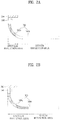
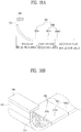
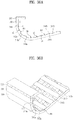
- FIGs. 1A and 1B are views explaining a backlight unit according to an embodiment.
- FIG. 1A is a sectional view of the backlight unit and
- FIG. 1B is a top perspective view of the backlight unit.
- the backlight unit may include a light source module 100 including at least one light source 110, a first reflector 200 and a second reflector 300.
- the light source module 100 including the light source 110, may be located between the first reflector 200 and the second reflector 300 and may be adjacent to the first reflector 200 or the second reflector 300.
- the light source module 100 may come into contact with the first reflector 200 while being spaced apart from the second reflector 300 by a predetermined distance, or may come into contact with the second reflector 300 while being spaced apart from the first reflector 200 by a predetermined distance.
- the light source module 100 may be spaced apart from both the first reflector 200 and the second reflector 300 by a predetermined distance, or may come into contact with both the first reflector 200 and the second reflector 300.
- the light source module 100 may include a circuit board having an electrode pattern and light emitting devices to generate light.
- At least one light emitting device may be mounted on the circuit board and the electrode pattern formed on the circuit board may connect the light emitting device to a power supply adaptor.
- a carbon nanotube electrode pattern may be formed on an upper surface of the circuit board so as to connect the light emitting device and the adaptor to each other.
- the circuit board may be a Printed Circuit Board (PCB) made of polyethylene terephthalate (PET), glass, polycarbonate (PC), silicon (Si) or the like, on which a plurality of light emitting devices is mounted, or may take the form of a film.
- PCB Printed Circuit Board
- PET polyethylene terephthalate
- PC polycarbonate
- Si silicon
- the circuit board may be selected from among a single-layer PCB, a multi-layer PCB, a ceramic board, a metal core PCB, and the like.
- the light emitting device may be a light emitting diode (LED) chip.
- the LED chip may be a blue LED chip or ultraviolet (UV) LED chip, or may be a package combining at least one or more selected from among a red LED chip, green LED chip, blue LED chip, yellow green LED chip, white LED chip and UV LED chip.
- a white LED may be realized by coupling a yellow phosphor to a blue LED, coupling both red and green phosphors to a blue LED, or coupling yellow, red and green phosphors to a blue LED.
- the first reflector 200 and the second reflector 300 may be spaced apart from each other by a predetermined distance so as to face each other so that an air guide is defined in a gap between the first reflector 200 and the second reflector 300 without a conventional light guide plate.
- the first reflector 200 may be made of a reflective coating film or a reflective coating material layer and may serve to reflect light emitted from the light source module 100 toward the second reflector 300.
- a saw-toothed reflective pattern may be formed on a surface of the first reflector 200 facing the light source module 100.
- the reflective pattern may have a flat surface or a curved surface.
- the surface of the first reflector 200 is provided with the reflective pattern so as to reflect light emitted from the light source module 100 toward a central region of the second reflector 300, thereby increasing luminance of a central region of the backlight unit.
- the second reflector 300 includes a specular reflection area 300a and a diffuse reflection area 300b.
- the specular reflection area 300a may serve to specularly reflect incident light and the diffuse reflection area 300b may serve to diffusely reflect incident light.
- the specular reflection area 300a and the diffuse reflection area 300b may have a light reflectivity of about 50 to 99.99%.
- the specular reflection area 300a may occupy about 5 to 50% of the entire area of the second reflector 300.
- the specular reflection area 300a may occupy about 20 to 30% of the entire area of the second reflector 300.
- a size ratio of the specular reflection area 300a to the diffuse reflection area 300b of the second reflector 300 may be 1:1 to 20.
- the size ratio of the specular reflection area 300a to the diffuse reflection area 300b of the second reflector 300 is set so as to reduce the difference of luminance between an area adjacent to the light source 110 and an area distant from the light source 110.
- the size ratio of the specular reflection area 300a to the diffuse reflection area 300b of the second reflector 300 may be properly adjusted to provide overall uniform luminance.
- the second reflector 300 may contain a metal or a metal oxide, such as aluminum (Al), silver (Ag), gold (Au) or titanium dioxide (TiO 2 ), exhibiting high reflectivity.
- the specular reflection area 300a and the diffuse reflection area 300b of the second reflector 300 may be formed of different materials. Also, the specular reflection area 300a and the diffuse reflection area 300b of the second reflector 300 may have different surface roughnesses.
- the specular reflection area 300a and the diffuse reflection area 300b of the second reflector 300 may be formed of the same material while having different surface roughnesses.
- the specular reflection area 300a and the diffuse reflection area 300b of the second reflector 300 may be formed of different materials while having different surface roughnesses.
- the light source 110 and/or the first reflector 200 may overlap with the specular reflection area 300a.
- the first reflector 200 may partially or fully overlap with the specular reflection area 300a of the second reflector 300.
- the specular reflection area 300a of the second reflector 300 may be located adjacent to the light source module 100 to reflect light emitted from the light source 110 to a central region of the second reflector 300.
- the diffuse reflection area 300b of the second reflector 300 may be located at the central region of the second reflector 300 to diffuse incident light.
- the second reflector 300 may include at least one inclined surface and at least one flat surface.
- the inclined surface of the second reflector 300 may be at a predetermined angle to the first reflector 200.
- the flat surface of the second reflector 300 may be parallel to the first reflector 200.
- the specular reflection area may be fully or partially formed at the inclined surface of the second reflector 300.
- the inclined surface of the second reflector 300 may overlap with the light source 110 and/or the first reflector 200.
- FIGs. 2A and 2B are views showing the first reflector overlapping with the specular reflection area of the second reflector.
- FIG. 2A is a view showing the first reflector partially overlapping with the specular reflection area of the second reflector.
- FIG. 2B is a view showing the first reflector fully overlapping with the specular reflection area of the second reflector.
- the first reflector 200 may partially overlap with the specular reflection area 300a of the second reflector 300.
- the light source 110 may be partially or fully overlap with the specular reflection area 300a of the second reflector 300.
- the first reflector 200 may fully overlap with the specular reflection area 300a of the second reflector 300.
- the light source 110 may be partially or fully overlap with the specular reflection area 300a of the second reflector 300.
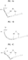
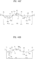
- FIGs. 3A to 3C are views showing the second reflector including the inclined surface and the flat surface.
- the inclined surface may have a planar surface and may be included in the specular reflection area 300a of the second reflector 300.
- the inclined surface may have a concavely curved surface and may be included in the specular reflection area 300a of the second reflector 300.
- the inclined surface may have a convexly curved surface and may be included in the specular reflection area 300a of the second reflector 300.
- the flat surface of the second reflector 300 parallel to the first reflector 200 may be included in the diffuse reflection area 300b of the second reflector 300.
- the second reflector 300 may include at least two inclined surfaces having at least one inflection point.
- the first and second inclined surfaces adjacent to each other about the inflection point may have different curvatures.
- FIGs. 4A to 4C are views showing a second reflector including a plurality of inclined surfaces.
- two inclined surfaces adjacent to each other have planar surfaces.
- One of the inclined surfaces may be included in the specular reflection area 300a of the second reflector 300 and the other inclined surface may be included in the diffuse reflection area 300b of the second reflector 300.
- the other inclined surface may be partially included in the specular reflection area 300a of the second reflector 300.
- two inclined surfaces adjacent to each other have concavely curved surfaces.
- the two inclined surfaces may have different curvatures.
- two inclined surfaces adjacent to each other have convexly curved surfaces.
- the two inclined surfaces may have different curvatures.
- One of the inclined surfaces may be included in the specular reflection area 300a of the second reflector 300 and the other inclined surface may be included in the diffuse reflection area 300b of the second reflector 300.
- the other inclined surface may be partially included in the specular reflection area 300a of the second reflector 300.
- the inclined surface of the second reflector 300 may be at least one selected from among a concave surface, a convex surface and a flat surface.
- the second reflector 300 may be a single layer or a double layer.
- the second reflector 300 may be configured to have a single layer including a specular reflection area 300a and a diffuse reflection area 300b.
- the second reflector 300 may be configured to have a double layer including a diffuse reflection layer and a specular reflection layer formed on the diffuse reflection layer so that the diffuse reflection layer is partially exposed.
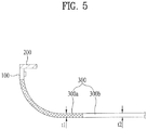
- FIG. 5 is a sectional view showing a second reflector of a single layer structure according to a first embodiment.
- the specular reflection area 300a and the diffuse reflection area 300b of the second reflector 300 do not overlap with each other.
- a specular reflection layer may be formed at the specular reflection area 300a of the second reflector 300 and a diffuse reflection layer may be formed at the diffuse reflection area 300b of the second reflector 300.
- the specular reflection layer and the diffuse reflection layer may be arranged on the same plane.
- the thickness t1 of the specular reflection layer may be equal to the thickness t2 of the diffuse reflection layer.
- the specular reflection layer and the diffuse reflection layer may contain a metal or a metal oxide, such as aluminum (Al), silver (Ag), gold (Au) or titanium dioxide (TiO 2 ), exhibiting high reflectivity.
- the specular reflection layer and the diffuse reflection layer may be formed of the same material or different materials. Also, the specular reflection layer and the diffuse reflection layer may have different surface roughnesses.
- the specular reflection layer and the diffuse reflection layer may be configured by attaching a reflective film to a mold body or may be a mold body having a specular reflection surface or a diffuse reflection surface.
- the specular reflection layer and the diffuse reflection layer may be formed of a copolymer resin, such as plastic, by injection molding.
- the reflective film may contain a metal and/or a metal oxide.
- the reflective layer may contain a metal or a metal oxide, such as aluminum (Al), silver (Ag), gold (Au) or titanium dioxide (TiO 2 ), exhibiting high reflectivity.
- a bonding agent or coupling member is formed at the interface between the specular reflection area 300a having the specular reflection layer and the diffuse reflection area 300b having the diffuse reflection layer to connect the specular reflection area 300a and the diffuse reflection area 300b to each other.
- the size percentage of the specular reflection area 300a of the second reflector 300 may decrease as the specular reflection area 300a becomes distant from the light source module 100.
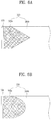
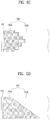
- FIGs. 6A to 6D are plan views showing various shapes of a second reflector having a specular reflection area, the size of which decreases as the specular reflection area becomes distant from a light source module.
- the specular reflection area 300a of the second reflector 300 may have a triangular shape.
- the specular reflection area 300a of the second reflector 300 may have a semicircular shape.
- the specular reflection area 300a of the second reflector 300 may have a stepwise shape.
- the specular reflection area 300a of the second reflector 300 may have a slant line.
- the size of the specular reflection area 300a of the second reflector 300 may gradually decrease as the specular reflection area 300a becomes distant from the light source module 100.
- the size of the diffuse reflection area 300b of the second reflector 300 may gradually increase as the diffuse reflection area 300b becomes distant from the light source module 100.
- the specular reflection area 300a of the second reflector 300 may occupy about 20 to 30% of the entire area of the second reflector 300.
- a size ratio of the specular reflection area 300a to the diffuse reflection area 300b of the second reflector 300 may be about 1:1 to 20.
- the specular reflection area 300a of the second reflector 300 is formed so that the size percentage of the specular reflection area 300a of the second reflector 300 decreases as the specular reflection area 300a becomes distant from the light source module 100 so as to remove black lines from the boundary between the specular reflection area 300a and the diffuse reflection area 300b, thereby providing uniform luminance.
- the specular reflection area 300a of the second reflector 300 may include a first area adjacent to the light source module 100 and a second area distant from the light source module 100.
- the specular reflection area 300a of the second reflector 300 adjacent to the light source module 100 may have a size greater than that of the specular reflection area 300a of the second reflector 300 distant from the light source module 100.
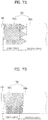
- FIGs. 7A to 7C are plan views showing various shapes of a second reflector having a specular reflection area, the size of which varies depending upon distance from the light source module.
- the second area of the specular reflection area 300a may have triangular shapes.
- the second area of the specular reflection area 300a may have semicircular shapes.
- the second area of the specular reflection area 300a may have square shapes.
- the specular reflection area 300a of the second reflector 300 may include a first area adjacent to the light source module 100 and a second area distant from the light source module 100.
- the second area of the specular reflection area 300a may have a size less than that of the first area of the specular reflection area 300a and may have various shapes, such as triangular shapes, semicircular shapes, square shapes and polygonal shapes.
- the size of the second area of the specular reflection area 300a may gradually decrease as the second area of the specular reflection area 300a becomes distant from the light source module 100.
- the size of the second area of the diffuse reflection area 300b may gradually increase as the second area of the diffuse reflection area 300b becomes distant from the light source module 100.
- the specular reflection area 300a of the second reflector 300 may occupy about 20 to 30% of the entire area of the second reflector 300.
- a size ratio of the specular reflection area 300a to the diffuse reflection area 300b of the second reflector 300 may be about 1:1 to 20.
- a size ratio of the first area to the second area of the specular reflection area 300a of the second reflector 300 may be about 1 to 10:0.4.
- the second area of the specular reflection area 300a may extend about 5 to 200 mm from the first area of the specular reflection area 300a.
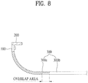
- FIG. 8 is a sectional view showing a second reflector of a single layer structure according to a second embodiment.
- the specular reflection area 300a and the diffuse reflection area 300b of the second reflector 300 overlap with each other.
- a specular reflection layer may be formed at the specular reflection area 300a of the second reflector 300 and a diffuse reflection layer may be formed at the diffuse reflection area 300b of the second reflector 300.
- the specular reflection layer and the diffuse reflection layer may be formed at the overlap area in an overlapping fashion.
- the overlap area may have a structure in which the specular reflection layer is deposited on the diffuse reflection layer.
- the overall thickness of the overlap area may be substantially equal to the thickness of the specular reflection area 300a of the second reflector 300 and the thickness of the diffuse reflection area 300b.
- the overall thickness of the overlap area may be different from the thickness of the specular reflection area 300a of the second reflector 300 and/or the thickness of the diffuse reflection area 300b.
- the overlap area may have a structure in which the diffuse reflection layer is deposited on the specular reflection layer.
- the specular reflection layer and the diffuse reflection layer of the second reflector 300 may be arranged on the same plane.
- the specular reflection layer and the diffuse reflection layer may partially overlap with each other.
- FIGs. 9A to 9D are sectional views showing various shapes of the overlap area of FIG. 8 .
- the thickness of the specular reflection layer of the overlap area is uniform. Referring to FIGs. 9A and 9D , the thickness of the specular reflection layer of the overlap area is uniform. In FIGs. 9B and 9C , the thickness of the specular reflection layer of the overlap area gradually decreases.
- the overlap area may have a structure in which the specular reflection layer and the diffuse reflection layer overlap with each other.
- the thickness t11 of the specular reflection layer overlapping with the diffuse reflection layer may be less than the thickness t1 of the specular reflection layer not overlapping with the diffuse reflection layer.
- the thickness t11 of the specular reflection layer formed at the overlap area may be less than the thickness t1 of the specular reflection layer formed at the specular reflection area 300a.
- the thickness t22 of the diffuse reflection layer formed at the overlap area may be less than the thickness t2 of the diffuse reflection layer formed at the diffuse reflection area 300b.
- the thickness t11 of the specular reflection layer formed at the overlap area may be uniform within the overlap area and may be equal to the thickness t22 of the diffuse reflection layer formed at the overlap area.
- the thickness t11 of the specular reflection layer formed at the overlap area may be greater than or less than the thickness t22 of the diffuse reflection layer formed at the overlap area.
- the thicknesses t11 and t12 of the specular reflection layer formed at the overlap area may be less than the thickness t1 of the specular reflection layer formed at the specular reflection area 300a.
- the thicknesses t11 and t12 of the specular reflection layer formed at the overlap area may gradually decrease as the specular reflection layer becomes distant from the light source module.
- the specular reflection layer formed at the overlap area may gradually decrease from the thickness t11 of the area adjacent to the light source module to the thickness t12 of the area distant from the light source module.
- the thicknesses t11 and t12 of the specular reflection layer formed at the overlap area may be less than the thickness t1 of the specular reflection layer formed at the specular reflection area 300a.
- the thicknesses t11 and t12 of the specular reflection layer formed at the overlap area may stepwise decrease as the specular reflection layer becomes distant from the light source module.
- the specular reflection layer formed at the overlap area may decrease from the thickness t11 of the area adjacent to the light source module to the thickness t12 of the area distant from the light source module.
- the overlap area may have a structure in which the diffuse reflection layer is disposed in the specular reflection layer.
- the thickness t11 of the specular reflection layer on the diffuse reflection layer and the thickness t12 of the specular reflection layer under the diffuse reflection layer may be less than the thickness t1 of the specular reflection layer formed at the specular reflection area 300a. Also, the thickness t22 of the diffuse reflection layer formed at the overlap area may be less than the thickness t2 of the diffuse reflection layer formed at the diffuse reflection area 300b.
- the thicknesses t11 and t12 of the specular reflection layer formed at the overlap area may be uniform within the overlap area and may be equal to the thickness t22 of the diffuse reflection layer formed at the overlap area.
- the thicknesses t11 and t12 of the specular reflection layer formed at the overlap area may be greater than or less than the thickness t22 of the diffuse reflection layer formed at the overlap area.
- FIGs. 10A to 10C are plan views showing various shapes of the specular reflection layer formed at the overlap area of FIG. 8 .
- the specular reflection layer of the overlap area may have triangular shapes.
- the specular reflection layer of the overlap area may have semicircular shapes.
- the specular reflection layer of the overlap area may have square shapes.
- the second reflector 300 may include an overlap area within which the specular reflection layer of the specular reflection area 300a and the diffuse reflection layer of the diffuse reflection area 300b overlap with each other.
- the specular reflection layer of the overlap area may have a size less than that of the specular reflection layer of the specular reflection area 300a and may have various shapes, such as triangular shapes, semicircular shapes, square shapes and polygonal shapes.
- the size of the specular reflection layer of the overlap area may gradually decrease as the specular reflection layer becomes distant from the light source module 100.
- the size of the diffuse reflection layer of the overlap area may gradually increase as the specular reflection layer becomes distant from the light source module 100.
- the specular reflection area 300a of the second reflector 300 may occupy about 20 to 30% of the entire area of the second reflector 300.
- a size ratio of the specular reflection area 300a to the diffuse reflection area 300b of the second reflector 300 may be about 1:1 to 20.
- a size ratio of the non-overlap area to the overlap area of the specular reflection area 300a of the second reflector 300 may be about 1 to 10:0.4.
- the overlap area of the specular reflection area 300a may extend about 5 to 200 mm from the specular reflection area 300a.
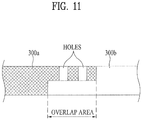
- At least one hole may be formed at the specular reflection layer of the overlap area so that the diffuse reflection layer is partially exposed.
- FIG. 11 is a sectional view showing holes of the specular reflection layer formed at the overlap area of FIG. 8 .
- FIGs. 12A and 12B are plan views showing the holes of the specular reflection layer formed at the overlap area of FIG. 8 .
- a plurality of holes may be formed at the specular reflection layer, formed on the diffuse reflection layer, of the overlap area so that the diffuse reflection layer is partially exposed.
- the number of holes formed at the specular reflection layer may increase as the holes become distant from the light source module.
- the holes formed at the specular reflection layer may have the same size. According to circumstances, the holes formed at the specular reflection layer may have different sizes.
- the holes formed at the overlap area may have the same size. As shown in FIG. 12B , the holes formed at the overlap area may have different sizes.
- the size of the holes may increase as the holes become distant from the light source module 100.
- the number of the holes formed at the overlap area may increase as the holes become distant from the light source module 100 irrespective of the size thereof.
- the holes are formed at the overlap area of the second reflector so that the size of the specular reflection area 300a decreases as the specular reflection area 300a becomes distant from the light source module 100, thereby providing uniform luminance.
- the specular reflection layer formed at the specular reflection area of the second reflector and the diffuse reflection layer formed at the diffuse reflection area of the second reflector may be configured by attaching a reflective film to a mold body or may be a mold body having a specular reflection surface or a diffuse reflection surface.
- the specular reflection layer and the diffuse reflection layer may be formed of a copolymer resin, such as plastic, by injection molding.
- the reflective film may contain a metal and/or a metal oxide.
- the reflective layer may contain a metal or a metal oxide, such as aluminum (Al), silver (Ag), gold (Au) or titanium dioxide (TiO 2 ), exhibiting high reflectivity.
- a bonding agent or coupling member is formed between the specular reflection area having the specular reflection layer and the diffuse reflection area having the diffuse reflection layer to connect the specular reflection area and the diffuse reflection area to each other.
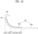
- FIG. 13 is a sectional view showing a second reflector of a double layer structure.
- the second reflector 300 is configured to have a structure in which the specular reflection area 300a and the diffuse reflection area 300b overlap with each other.
- the second reflector 300 may have a double layer including a diffuse reflection layer and a specular reflection layer formed on the diffuse reflection layer so that the diffuse reflection layer is partially exposed.
- the specular reflection area 300a of the second reflector 300 has a structure in which the specular reflection layer is formed on the diffuse reflection layer
- the diffuse reflection area 300b of the second reflector 300 has a structure in which the diffuse reflection layer is exposed.
- the specular reflection area 300a of the second reflector 300 may occupy about 20 to 30% of the entire area of the second reflector 300. According to circumstances, a size ratio of the specular reflection area 300a to the diffuse reflection area 300b of the second reflector 300 may be 1:1 to 20.
- the specular reflection area 300a may include a first area adjacent to the light source module 100 and a second area distant from the light source module 100.
- the second area may have a size less than that of the first area.
- a size ratio of the first area to the second area of the specular reflection area 300a of the second reflector 300 may be about 1 to 10:0.4.
- the thickness of the specular reflection layer formed at the second area of the specular reflection area 300a of the second reflector 300 may be equal to or different from that of the specular reflection layer formed at the first area of the specular reflection area 300a of the second reflector 300.
- FIGs. 14A and 14B are sectional views showing thicknesses of the specular reflection area of FIG. 13 .
- the thickness of the specular reflection layer formed at the second area gradually decreases as the specular reflection layer becomes distant from the light source module (not shown).
- the thickness of the specular reflection layer formed at the second area remains uniform and then gradually decreases as the specular reflection layer becomes distant from the light source module (not shown).
- the thicknesses t11 and t12 of the specular reflection layer formed at the second area of the specular reflection area 300a may be less than the thickness t1 of the specular reflection layer formed at the first area of the specular reflection area 300a.
- the thicknesses t11 and t12 of the specular reflection layer formed at the second area may gradually decrease as the specular reflection layer becomes distant from the light source module.
- the specular reflection layer formed at the second area may gradually decrease from the thickness t11 of the area adjacent to the light source module to the thickness t12 of the area distant from the light source module.
- the thicknesses t11 and t12 of the specular reflection layer formed at the second area of the specular reflection area 300a may be equal to the thickness t1 of the specular reflection layer formed at the first area of the specular reflection area 300a and then may gradually decrease.
- the specular reflection layer formed at the second area may decrease from the thickness t11 of the area adjacent to the light source module to the thickness t12 of the area distant from the light source module.
- the thickness of the specular reflection layer formed at the second area is reduced so as to reduce abrupt change of luminance at the boundary between the specular reflection area 300a and the diffuse reflection area 300b.
- a plurality of holes may be formed at the specular reflection layer formed on the diffuse reflection layer so that the diffuse reflection layer is partially exposed.
- FIGs. 15A and 15B are plan views showing holes formed at the specular reflection area.
- the number of holes formed at the specular reflection area 300a may increase as the holes become distant from the light source module 100.
- the size of holes formed at the specular reflection area 300a may increase as the holes become distant from the light source module 100.
- a plurality of holes may be formed at the specular reflection layer, formed on the diffuse reflection layer, of the specular reflection area 300a so that the diffuse reflection layer is partially exposed.
- the number of holes formed at the specular reflection layer may increase as the holes become distant from the light source module 100.
- the holes formed at the specular reflection layer may have the same size. According to circumstances, the holes formed at the specular reflection layer may have different sizes.
- both the number and size of the holes formed at the specular reflection layer may increase as the holes become distant from the light source module 100.
- a plurality of holes may be formed at the specular reflection layer, formed on the diffuse reflection layer, of the specular reflection area 300a so that the diffuse reflection layer is partially exposed.
- the size of holes formed at the specular reflection layer may increase as the holes become distant from the light source module 100.
- the holes formed at the specular reflection layer may have the same number. According to circumstances, the holes formed at the specular reflection layer may have different numbers.
- both the number and size of the holes formed at the specular reflection layer may increase as the holes become distant from the light source module 100.
- the holes are formed at the specular reflection area 300a of the second reflector 300 so that the size percentage of the specular reflection area 300a decreases as the specular reflection area 300a becomes distant from the light source module 100, thereby providing uniform luminance.
- the specular reflection area 300a may include a first area adjacent to the light source module 100 and a second area distant from the light source module 100.
- the second area may have a size less than that of the first area.
- FIGs. 16A to 16C are plan views showing various shapes of the second area of the specular reflection area.
- the second area of the specular reflection area 300a may have triangular shapes.
- the second area of the specular reflection area 300a may have semicircular shapes.
- the second area of the specular reflection area 300a may have square shapes.
- the specular reflection area 300a of the second reflector 300 may include a first area adjacent to the light source module 100 and a second area distant from the light source module 100.
- the second area of the specular reflection area 300a may have a size less than that of the first area of the specular reflection area 300a and may have various shapes, such as triangular shapes, semicircular shapes, square shapes and polygonal shapes.
- the size of the second area of the specular reflection area 300a may gradually decrease as the second area of the specular reflection area 300a becomes distant from the light source module 100.
- the size of the second area of the diffuse reflection area 300b may gradually increase as the second area of the diffuse reflection area 300b becomes distant from the light source module 100.
- the specular reflection area 300a of the second reflector 300 may occupy about 20 to 30% of the entire area of the second reflector 300.
- a size ratio of the specular reflection area 300a to the diffuse reflection area 300b of the second reflector 300 may be about 1:1 to 20.
- a size ratio of the first area to the second area of the specular reflection area 300a of the second reflector 300 may be about 1 to 10:0.4.
- the second area of the specular reflection area 300a may extend about 5 to 200 mm from the first area of the specular reflection area 300a.
- the specular reflection layer formed at the specular reflection area 300a of the second reflector 300 and the diffuse reflection layer formed at the diffuse reflection area 300b of the second reflector 300 may be configured by attaching a reflective film to a mold body or a metal body or may be a mold body or a metal body having a specular reflection surface or a diffuse reflection surface.
- the specular reflection layer and the diffuse reflection layer may be formed of a copolymer resin, such as plastic, by injection molding.
- the reflective film may contain a metal and/or a metal oxide.
- the reflective layer may contain a metal or a metal oxide, such as aluminum (Al), silver (Ag), gold (Au) or titanium dioxide (TiO 2 ), exhibiting high reflectivity.
- a bonding agent or coupling member is formed at the interface between the specular reflection area 300a having the specular reflection layer and the diffuse reflection area 300b having the diffuse reflection layer to connect the specular reflection area 300a and the diffuse reflection area 300b to each other.
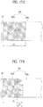
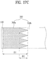
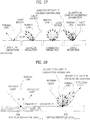
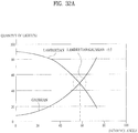
- FIGs. 17A to 17C and 18 are views explaining uniformity of luminance depending upon shapes of the specular reflection area of the second reflector.
- FIG. 17A no triangular shape is formed at one end point of the specular reflection area.
- FIGs. 17B and 17C triangular shapes are formed at one end point of the specular reflection area.
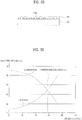
- FIG. 18 is a graph showing comparison of uniformity of luminance between embodiments shown in FIGs. 17A to 17C .
- a second reflector having only a diffuse reflection area without a specular reflection area although not shown is embodiment A
- a second reflector 300 having a specular reflection area 300a having a distance D1 between opposite end points of about 100 mm as shown in FIG. 17A is embodiment B
- a second reflector 300 having triangular shapes, each of which has a distance D2 (that is, the height of each of the triangular shapes) between opposite end points of about 90 mm, within a specular reflection area 300a having a distance D1 between opposite end points of about 100 mm as shown in FIG. 17C is embodiment D.
- FIG. 18 is a graph showing comparison of luminance between the respective embodiments based on distance from a light source.
- the luminance of the area adjacent to the light source is high and the luminance of the area distant from the light source is low.
- embodiment D having the triangular shapes each of which has a height of about 90 mm exhibits higher and more uniform luminance than embodiment C having the triangular shapes each of which has a height of about 30 mm.
- the specular reflection area of the second reflector may include a first area adjacent to the light source module and a second area distant from the light source module. It can be seen that luminance is uniform in a case in which the second area of the specular reflection area gradually decreases as the second area becomes distant from the light source.
- FIG. 19 is a view showing a specular reflection area having holes and triangular shapes.
- a specular reflection layer having a plurality of holes may be formed at the first area of the specular reflection area 300a, and a specular reflection layer having triangular shapes may be formed at the second area of the specular reflection area 300a.
- a diffuse reflection layer located under the specular reflection layer may be exposed through the holes formed at the first area.
- the number or size of the holes of the specular reflection layer formed at the first area of the specular reflection area 300a and the shape of the specular reflection layer formed at the second area of the specular reflection area 300a may be properly adjusted to provide overall uniform luminance.
- FIGs. 20A and 20B are views showing a specular reflection area having stripe shapes.
- a specular reflection layer may be formed at the first area of the specular reflection area 300a, and a specular reflection layer having stripe shapes may be formed at the second area of the specular reflection area 300a.
- the specular reflection layer formed at the second area of the specular reflection area 300a has a plurality of stripes.
- the stripes may have the same width or different widths.
- FIG. 20A a plurality of stripes having the same width are arranged at the second area of the specular reflection area 300a.
- FIG. 20B a plurality of stripes having different widths are arranged at the second area of the specular reflection area 300a.
- the width w1 of a stripe adjacent to the light source module 100 may greater than the width w3 of a stripe distant from the light source module 100.
- a plurality holes may be formed at the specular reflection layer formed at the first area of the specular reflection area 300a, and a diffuse reflection layer located under the specular reflection layer may be exposed through the holes.
- the number and width of the stripes formed at the second area of the specular reflection area 300a may be properly adjusted to provide overall uniform luminance.
- the second reflector having the specular reflection area and the diffuse reflection area may be configured to have various shapes based on the arrangement of the light source module.
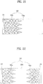
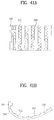
- FIG. 21 is a view showing a one edge type second reflector.
- FIG. 22 is a view showing a two edge type second reflector.
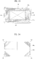
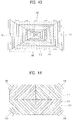
- FIGs. 23 and 24 are views showing four edge type second reflectors.
- FIG. 21 is a plan view of the one edge type second reflector. As shown in FIG. 21 , a light source module 100 may be disposed at one side of the one edge type second reflector 300. A specular reflection area 300a may be adjacent to the light source module 100. A diffuse reflection area 300b may be distant from the light source module 100.
- FIG. 22 is a plan view of the two edge type second reflector. As shown in FIG. 22 , light source modules 100 may be disposed at opposite sides of the two edge type second reflector 300. Specular reflection areas 300a may be adjacent to the respective light source modules 100. A diffuse reflection area 300b may be distant from the light source modules 100.
- FIG. 23 is a plan view of the four edge type second reflector. As shown in FIG. 23 , light source modules 100 may be disposed at four sides of the four edge type second reflector 300. Specular reflection areas 300a may be adjacent to the respective light source modules 100. Diffuse reflection areas 300b may be distant from the respective light source modules 100.
- FIG. 24 is a plan view of the four edge type second reflector. As shown in FIG. 24 , light source modules 100 may be disposed at four corners of the four edge type second reflector 300. Specular reflection areas 300a may be adjacent to the respective light source modules 100. Diffuse reflection areas 300b may be distant from the respective light source modules 100.
- the backlight unit according to the embodiment may further include an optical member spaced a predetermined distance from the second reflector.
- An air guide may be defined between the second reflector and the optical member.
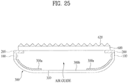
- FIG. 25 is a view showing a backlight unit including an optical member.
- FIG. 26 is a view showing an example of a shape of the optical member.
- the optical member 600 may be disposed at the open area of the first reflector 200.
- the optical member 600 may have several layers.
- An uneven pattern 620 may be provided at the uppermost layer or another layer.
- the optical member 600 may include at least one sheet selected from among a diffusion sheet, prism sheet, luminance increasing sheet and the like.
- the diffusion sheet serves to diffuse light emitted from a light source
- the prism sheet serves to guide the diffused light to a light emission area
- the luminance increasing sheet serves to increase luminance
- the optical member 600 is provided to diffuse light emitted through the open area of the first reflector 200.
- the uneven pattern 620 may be formed at an upper surface of the optical member 600 so as to improve a diffusion effect.
- the uneven pattern 620 may have stripe shapes arranged along the light source modules 100.
- the uneven pattern 620 may have protrusion parts formed at the surface of the optical member 600.
- Each of the protrusion parts may have a first surface and second surface which face each other.
- An angle between the first surface and second surface may be an obtuse angle or an acute angle.
- the optical member 600 may include at least one sheet selected from among a diffusion sheet, prism sheet, luminance increasing sheet and the like.
- the diffusion sheet serves to diffuse light emitted from a light source
- the prism sheet serves to guide the diffused light to a light emission area
- the luminance increasing sheet serves to increase luminance
- the diffuse reflection area 300b of the second reflector 300 may reflect incident light in a Lambertian distribution and/or a Gaussian distribution.
- the quantity of light reflected in the Lambertian distribution may be greater or less than the quantity of light reflected in the Gaussian distribution when an incidence angle of light incident upon each of the points is about 55 degrees or more with respect to a normal line passing each of the points.
- a reflective sheet exhibiting a specular reflection property may be disposed at the specular reflection area 300a of the second reflector 300, and a reflective sheet exhibiting a diffuse reflection property may be disposed at the diffuse reflection area 300b of the second reflector 300.
- a reflective sheet exhibiting diffuse reflection properties in which light is reflected in the Lambertian distribution and the Gaussian distribution may be disposed at the diffuse reflection area 300b of the second reflector 300.
- the reflective sheet disposed at the diffuse reflection area 300b may exhibit a diffuse reflection property in which the quantity of light reflected in the Gaussian distribution is greater than the quantity of light reflected in the Lambertian distribution.
- the reflective sheet disposed at the diffuse reflection area 300b may exhibit a diffuse reflection property in which the quantity of light reflected in the Gaussian distribution is greater than the quantity of light reflected in the Lambertian distribution.
- the reflective sheet disposed at the diffuse reflection area 300b may exhibit a diffuse reflection property in which a ratio of quantity of light reflected in the Lambertian distribution to quantity of light reflected in the Gaussian distribution is 5:5.
- FIG. 27 is a view explaining a specular reflection property and diffuse reflection property of light.
- light may be specularly reflected or diffusely reflected based on a surface property of the reflector.
- the diffuse reflection may include Gaussian reflection, Lambertian reflection and mixed reflection.
- the specular reflection is reflection in which, when light is incident upon a point of the reflector, an angle between a normal line passing the point and an optical axis of the incident light is equal to an angle between the normal line and an optical axis of reflected light.
- the Gaussian reflection is reflection in which intensity of reflected light based on angle at the surface of the reflector and an angle between a normal line and the reflected light vary according to values of a Gaussian function.
- the Lambertian reflection is reflection in which intensity of reflected light based on angle at the surface of the reflector and an angle between a normal line and the reflected light vary according to values of a cosine function.
- the mixed reflection includes at least one selected from among specular reflection, Gaussian reflection and Lambertian reflection.
- the surface property of the second reflector 300 may be adjusted to control a reflection property of light.
- FIG. 28 is a view showing distribution of light reflected at the diffuse reflection area of FIG. 1A .
- an angle ⁇ 1 between an optical axis of the incident light and a normal line passing the first point may be equal to an angle ⁇ 1 between an optical axis of light reflected from the first point and the normal line.
- light reflected from the second point may be reflected in a Lambertian distribution or a Gaussian distribution.
- the quantity of light reflected in the Gaussian distribution may be greater than the quantity of light reflected in the Lambertian distribution.
- the quantity of light reflected in the Gaussian distribution may be greater than the quantity of light reflected in the Lambertian distribution.
- the reflective sheet disposed at the diffuse reflection area 300b may exhibit a diffuse reflection property in which a ratio of quantity of light reflected in the Lambertian distribution to quantity of light reflected in the Gaussian distribution is 5:5.
- the second reflector 300 is configured so that the second reflector 300 exhibits a light reflection property so as to reduce the difference of luminance between the area adjacent to the light source 100 and the area distant from the light source 100.
- the specular reflection area 300a adjacent to the light source 110 may serve to specularly reflect light and to transmit the light to a central area of the backlight at which luminance is low.
- the diffuse reflection area 300b distant from the light source 110 may serve to diffusely reflect light to compensate for low luminance.
- the light reflection properties of the specular reflection area 300a and the diffuse reflection area 300b of the second reflector 300 may be properly adjusted to provide overall uniform luminance.
- the second reflector 300 may contain a metal or a metal oxide, such as aluminum (Al), silver (Ag), gold (Au) or titanium dioxide (TiO 2 ), exhibiting high reflectivity.
- the specular reflection area 300a and the diffuse reflection area 300b of the second reflector 300 may be formed of different materials. Also, the specular reflection area 300a and the diffuse reflection area 300b may have different surface roughnesses.
- the specular reflection area 300a and the diffuse reflection area 300b of the second reflector 300 may be formed of the same material while having different surface roughnesses.
- the specular reflection area 300a and the diffuse reflection area 300b of the second reflector 300 may be formed of different materials while having different surface roughnesses.
- the diffuse reflection area 300b of the second reflector 300 may include a first layer formed of polyethylene terephthalate (PET) and a second layer disposed on the first layer, the second layer being formed of TiO 2 and/or SiO 2 particles.
- PET polyethylene terephthalate
- the second layer being formed of TiO 2 and/or SiO 2 particles.
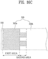
- FIG. 29 is a sectional view showing the construction of the diffuse reflection area of the second reflector.
- the diffuse reflection area of the second reflector may be configured to have a structure in which a second layer 304 is deposited on a first layer 302.
- the first layer 302 may be formed of polyethylene terephthalate (PET).
- the second layer 304 may be formed of TiO 2 and/or SiO 2 particles 304a.
- the particles 304a of the second layer 304 may have the same size or different sizes.
- the particles 304a of the second layer 304 may occupy about 20 to 90% of the entire area of the first layer 302.
- the size of the particles 304a may be about 5 to 50 um.
- a passivation layer may be further formed on the second layer 304.
- the weight of particles contained in the second layer 304 of the diffuse reflection area of the second reflector may be adjusted to control a light reflection property of the diffuse reflection area 300b.
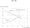
- FIG. 30 is a graph showing a light reflection property of the diffuse reflection area.
- the light reflection property of the diffuse reflection area may be controlled as indicated in Table 1 to configure the diffuse reflection area so that the quantity of light reflected in the Gaussian distribution is greater than the quantity of light reflected in the Lambertian distribution based on the incidence angle of light or so that the quantity of light reflected in the Lambertian distribution is greater than the quantity of light reflected in the Gaussian distribution based on the incidence angle of light.
- the reflective sheet disposed at the diffuse reflection area 300b may exhibit a diffuse reflection property in which a ratio of quantity of light reflected in the Lambertian distribution to quantity of light reflected in the Gaussian distribution is 5:5.
- the diffuse reflection area 300b of the second reflector 300 may occupy about 50 to 95% of the entire area of the second reflector 300.
- the diffuse reflection area 300b may occupy about 70 to 80% of the entire area of the second reflector 300.
- a size ratio of the specular reflection area 300a to the diffuse reflection area 300b of the second reflector 300 may be 1:1 to 20.
- the size ratio of the specular reflection area 300a to the diffuse reflection area 300b of the second reflector 300 is set so as to reduce the difference of luminance between an area adjacent to the light source 110 and an area distant from the light source 110.
- the size ratio of the specular reflection area 300a to the diffuse reflection area 300b of the second reflector 300 may be properly adjusted to provide overall uniform luminance.
- the diffuse reflection area 300b may include a plurality of diffuse reflection areas exhibiting different light reflection properties.
- FIGs. 31A and 31B are views showing a second reflector having a plurality of diffuse reflection areas exhibiting different light reflection properties.
- FIG. 31A is a sectional view of the second reflector
- FIG. 31B is a top perspective view of the second reflector.
- the backlight unit may include a light source module 100 including at least one light source 110, a first reflector 200 and a second reflector 300.
- the second reflector 300 may include a specular reflection area 300a and a diffuse reflection area 300b.
- the diffuse reflection area 300b may include a first diffuse reflection area 300b1 and a second diffuse reflection area 300b2.
- the specular reflection area 300a may serve to specularly reflect incident light.
- the diffuse reflection area 300b may serve to diffusely reflect incident light.
- the specular reflection area 300a and the diffuse reflection area 300b may have a light reflectivity of about 50 to 99.99%.
- the first and second diffuse reflection areas 300b1 and 300b2 may reflect incident light in a Lambertian distribution and/or a Gaussian distribution.
- the quantity of light reflected in the Gaussian distribution may be greater than the quantity of light reflected in the Lambertian distribution when an incidence angle of light incident upon each of the points is about 55 degrees or more with respect to a normal line passing each of the points.
- the quantity of light reflected in the Gaussian distribution may be greater than the quantity of light reflected in the Lambertian distribution when an incidence angle of light incident upon each of the points is about 60 degrees or more with respect to a normal line passing each of the points.
- the quantity of light reflected in the Gaussian distribution may be greater than the quantity of light reflected in the Lambertian distribution.
- the quantity of light reflected in the Lambertian distribution may be greater than the quantity of light reflected in the Gaussian distribution.
- a reflective sheet exhibiting a specular reflection property may be disposed at the specular reflection area 300a of the second reflector 300, and a reflective sheet exhibiting a diffuse reflection property may be disposed at the diffuse reflection area 300b of the second reflector 300.
- a reflective sheet exhibiting diffuse reflection properties in which light is reflected in the Lambertian distribution and the Gaussian distribution may be disposed at the diffuse reflection area 300b of the second reflector 300.
- the reflective sheet disposed at the first diffuse reflection area 300b1 may exhibit a diffuse reflection property in which the quantity of light reflected in the Gaussian distribution is greater than the quantity of light reflected in the Lambertian distribution.
- the reflective sheet disposed at the second diffuse reflection area 300b2 may exhibit a diffuse reflection property in which the quantity of light reflected in the Gaussian distribution is greater than the quantity of light reflected in the Lambertian distribution.
- the first diffuse reflection area 300b1 may exhibit a diffuse reflection property in which the quantity of light reflected in the Gaussian distribution is greater than the quantity of light reflected in the Lambertian distribution.
- the second diffuse reflection area 300b2 may exhibit a diffuse reflection property in which the quantity of light reflected in the Lambertian distribution is greater than the quantity of light reflected in the Gaussian distribution.
- the reflective sheet disposed at the diffuse reflection area 300b may exhibit a diffuse reflection property in which a ratio of quantity of light reflected in the Lambertian distribution to quantity of light reflected in the Gaussian distribution is 5:5.
- the second reflector 300 is configured so that the second reflector 300 exhibits a light reflection property so as to reduce the difference of luminance between the area adjacent to the light source 100 and the area distant from the light source 100.
- the specular reflection area 300a adjacent to the light source 110 may serve to specularly reflect light and to transmit the light to a central area of the backlight at which luminance is low.
- the first and second diffuse reflection areas 300b1 and 300b2 distant from the light source 110 may serve to diffusely reflect light to compensate for low luminance.
- the light reflection properties of the specular reflection area 300a and the first and second diffuse reflection areas 300b1 and 300b2 of the second reflector 300 may be properly adjusted to provide overall uniform luminance.
- the second reflector 300 may contain a metal or a metal oxide, such as aluminum (Al), silver (Ag), gold (Au) or titanium dioxide (TiO 2 ), exhibiting high reflectivity.
- the specular reflection area 300a and the first and second diffuse reflection areas 300b1 and 300b2 of the second reflector 300 may be formed of different materials. Also, the specular reflection area 300a and the first and second diffuse reflection areas 300b1 and 300b2 may have different surface roughnesses.
- the specular reflection area 300a and the first and second diffuse reflection areas 300b1 and 300b2 of the second reflector 300 may be formed of the same material while having different surface roughnesses.
- the specular reflection area 300a and the first and second diffuse reflection areas 300b1 and 300b2 of the second reflector 300 may be formed of different materials while having different surface roughnesses.
- the diffuse reflection area 300b of the second reflector 300 may include a first layer formed of polyethylene terephthalate (PET) and a second layer disposed on the first layer, the second layer being formed of TiO 2 and/or SiO 2 particles.
- PET polyethylene terephthalate
- the second layer being formed of TiO 2 and/or SiO 2 particles.
- the first and second diffuse reflection areas 300b1 and 300b2 may contain the same material.
- the particle weight of the material contained in the first diffuse reflection area 300b1 may be different from that of the material contained in the second diffuse reflection area 300b2.
- the particle weight of the material contained in the first diffuse reflection area 300b1 may be less than that of the material contained in the second diffuse reflection area 300b2.
- first and second diffuse reflection areas 300b1 and 300b2 may have different surface roughnesses depending upon particle weight.
- the particle weight of the material contained in the first diffuse reflection area 300b1 may occupy about 20 to 90% of the entire size of the first diffuse reflection area 300b1.
- the particle weight of the material contained in the second diffuse reflection area 300b2 may occupy about 20 to 90% of the entire size of the second diffuse reflection area 300b2.
- first and second diffuse reflection areas 300b1 and 300b2 may contain the same amount of the same material.
- the particle size of the material contained in the first diffuse reflection area 300b1 may be different from that of the material contained in the second diffuse reflection area 300b2.
- the particle size of the material contained in the first diffuse reflection area 300b1 may be about 5 to 50 um.
- the particle weight or size of the material contained in the first and second diffuse reflection areas 300b1 and 300b2 of the second reflector may be adjusted to control light reflection properties of the first and second diffuse reflection areas 300b1 and 300b2.
- the size of the first diffuse reflection area 300b1 may be equal to or less than that of the second diffuse reflection area 300b2.
- a size ratio of the first diffuse reflection area 300b1 to the second diffuse reflection area 300b2 may be 1:1 to 5.
- the size of the specular reflection area 300a may be equal to or less than that of the first diffuse reflection area 300b1.
- a size ratio of the specular reflection area 300a to the first diffuse reflection area 300b1 may be 1:1 to 4.
- the size of the specular reflection area 300a may be equal to or less than that of the second diffuse reflection area 300b2.
- a size ratio of the specular reflection area 300a to the second diffuse reflection area 300b2 may be 1:1 to 20.
- first diffuse reflection area 300b1 may be disposed between the specular reflection area 300a and the second diffuse reflection area 300b2.
- the distance between the specular reflection area 300a and the light source 110 is less than that between the first diffuse reflection area 300b1 and the light source 110.
- the distance between the first diffuse reflection area 300b1 and the light source 110 is less than that between the second diffuse reflection area 300b2 and the light source 110.
- FIG. 32A is a graph showing a light reflection property of the first diffuse reflection area.
- FIG. 32B is a graph showing a light reflection property of the second diffuse reflection area.
- the light reflection property of the diffuse reflection area may be controlled as indicated in Tables 2 and 3 to configure the diffuse reflection area so that the quantity of light reflected in the Gaussian distribution is greater than the quantity of light reflected in the Lambertian distribution based on the incidence angle of light or so that the quantity of light reflected in the Lambertian distribution is greater than the quantity of light reflected in the Gaussian distribution based on the incidence angle of light.
- the reflective sheet disposed at the diffuse reflection area 300b may exhibit a diffuse reflection property in which a ratio of quantity of light reflected in the Lambertian distribution to quantity of light reflected in the Gaussian distribution is 5:5.
- the diffuse reflection area may be divided into two areas exhibiting different light reflection properties. According to circumstances, the diffuse reflection area may be divided into three to ten areas exhibiting different light reflection properties.
- the diffuse reflection areas of the second reflector may be designed to exhibit optimal light reflection properties based on overall size and structure of the backlight unit.
- the second reflector having the specular reflection area and the first and second diffuse reflection areas may be configured to have various shapes based on the arrangement of the light source module.
- FIGs. 31A and 31B are views showing a one edge type second reflector.
- the light source module 100 may be disposed at one side of the one edge type second reflector 300.
- the specular reflection area 300a may be adjacent to the light source module 100.
- the first and second diffuse reflection areas 300b1 and 300b2 may be distant from the light source module 100.
- FIG. 33 is a view showing a two edge type second reflector.
- FIGs. 34 and 35 are views showing four edge type second reflectors.
- FIG. 33 is a plan view of the two edge type second reflector. As shown in FIG. 33 , light source modules 100 may be disposed at opposite sides of the two edge type second reflector 300. Specular reflection areas 300a may be adjacent to the respective light source modules 100. First and second diffuse reflection areas 300b1 and 300b2 may be distant from the respective light source modules 100.
- FIG. 34 is a plan view of the four edge type second reflector. As shown in FIG. 34 , light source modules 100 may be disposed at four sides of the four edge type second reflector 300. Specular reflection areas 300a may be adjacent to the respective light source modules 100. First and second diffuse reflection areas 300b1 and 300b2 may be distant from the respective light source modules 100.
- FIG. 35 is a plan view of the four edge type second reflector. As shown in FIG. 35 , light source modules 100 may be disposed at four corners of the four edge type second reflector 300. Specular reflection areas 300a may be adjacent to the respective light source modules 100. First and second diffuse reflection areas 300b1 and 300b2 may be distant from the respective light source modules 100.
- the backlight unit according to the embodiment may further include an optical member spaced a predetermined distance from the second reflector.
- An air guide may be defined between the second reflector and the optical member.
- the second reflector may have a plurality of patterns.
- FIGs. 36A and 36B are views showing a second reflector having a plurality of diffuse reflection areas exhibiting different light reflection properties.
- FIG. 36A is a sectional view of the second reflector and
- FIG. 36B is a top perspective view of the second reflector.
- the second reflector 300 may include an inclined surface 310 having at least one inflection point P0.
- the second reflector 300 may have a plurality of patterns in which concave lines 312 and convex lines 314 are alternately arranged along the inclined surface 310 in one direction.
- the concave lines 312 of the second reflector 300 may be concavely curved from the inclined surface 310.
- the convex lines 314 of the second reflector 300 may be convexly curved from the inclined surface 310.
- the inclined surface 310 of the second reflector 300 may be at a predetermined angle to the horizontal surface parallel to the surface of the first reflector 200.
- the second reflector 300 may include at least two inclined surfaces 310 having at least one inflection point P0. As shown in FIGs. 36A and 36B , the second reflector 300 may include a first inclined surface 310a having a first curvature R1 and a second inclined surface 310b having a second curvature R2.
- curvatures R1 and R2 the first and second inclined surfaces 310a and 310b adjacent to each other about the inflection point P0 of the second reflector 300 may be different from each other.
- the curvature R1 of the first inclined surface 310a adjacent to the light source module 100 may be greater than the curvature R21 of the second inclined surface 310b adjacent to the first inclined surface 310a.
- the concave lines 312 and convex lines 314 of the second reflector 300 may be alternately arranged along the first and second inclined surfaces 310a and 310b in one direction.
- the concave lines 312 having concavely curved surfaces and the convex lines 314 having convexly curved surfaces may be arranged in the same direction as the direction in which light sources of the light source module 100 are arranged.
- the concave lines 312 and convex lines 314 may include first concave lines 312a and first convex lines 314a arranged along the first inclined surface 310a. Also, the concave lines 312 and the convex lines 314 may include second concave lines 312b and second convex lines 314b arranged along the second inclined surface 310b.
- the first concave lines 312a and first convex lines 314a arranged along the first inclined surface 310a may have a first curvature r1 and second curvature r2, respectively.
- the second concave lines 312b and second convex lines 314b arranged along the second inclined surface 310b may have a third curvature r3 and fourth curvature r4, respectively.
- the first curvature r1, second curvature r2, third curvature r3 and fourth curvature r4 may be the same. According to circumstances, at least one of the curvatures may be different from the other curvatures.
- first curvature r1 and second curvature r2 of the first concave lines 312a and first convex lines 314a arranged along the first inclined surface 310a may be equal to or different from the third curvature r3 and fourth curvature r4 of the second concave lines 312b and second convex lines 314b arranged along the second inclined surface 310b.
- the first curvature r1 and second curvature r2 of the first concave lines 312a and first convex lines 314a arranged along the first inclined surface 310a may be greater than the third curvature r3 and fourth curvature r4 of the second concave lines 312b and second convex lines 314b arranged along the second inclined surface 310b.
- first concave lines 312a and first convex lines 314a arranged along the first inclined surface 310a reflect light emitted from the light source 110 to the central area of the second reflector 300 to provide uniform luminance.
- FIG. 37 is a view showing the concave lines and convex lines of FIG. 36A in detail.
- the concave lines 312 and convex lines 314 of the second reflector 300 may be alternately arranged along the inclined surface 310 of the second reflector 300.
- the concave lines 312 may have surfaces concavely curved from the inclined surface 310 so as to have the first curvature r1.
- each of the concave lines 312 may have a curved surface passing a contact point P2 between each of the concave lines 312 and the inclined surface 310 and a peak point P3 of each of the concave lines.
- the width W1 of each of the concave lines 312 corresponds to the distance between two straight lines perpendicular to the inclined surface 310 and passing the respective contact points P2.
- the convex lines 314 may have surfaces convexly curved from the inclined surface 310 so as to have the second curvature r2.
- each of the convex lines 314 may have a curved surface passing a contact point P2 between each of the convex lines 314 and the inclined surface 310 and a peak point P1 of each of the convex lines.
- the width W2 of each of the convex lines 314 corresponds to the distance between two straight lines perpendicular to the inclined surface 310 and passing the respective contact points P2.
- the curvatures of the concave lines and convex lines may be decided based on a predetermined equation.
- FIG. 38 is a view explaining a condition to decide curvature of the concave lines or the convex lines of FIG. 36A .
- the curvature r1 of each concave line 312 may satisfy a condition that an angle ⁇ between the straight line connecting the contact point P2 between the concave line 312 and the inclined surface 310 and the peak point P3 of the concave line 312 and the inclined surface 310 is about 0.01 to 15 degrees.
- h indicates the maximum depth of the concave line 312, which is the minimum distance between the peak point P3 of the concave line 312 and the inclined surface 310.
- W indicates the width of the concave line 312, which is the minimum distance between the contact point P2 between the concave line 312 and the inclined surface 310 and the vertical line connecting the peak point P3 of the concave line 312 and the inclined surface 310.
- equation 1 may be derived from the following numerical expression.
- the angle ⁇ between the straight line connecting the contact point P2 between the concave line 312 and the inclined surface 310 and the peak point P3 of the concave line 312 and the inclined surface 310 may be tan -1 (h/W), which is about 0.01 to 15 degrees.
- the concave line 312 is formed to have the curvature based on the condition of the angle ⁇ , a shadow effect does not occur due to the curved surface of the concave line when light is incident upon the concave line with the result that an apparent black area does not appear, and therefore, it is possible to manufacture a backlight unit exhibiting uniform luminance.
- Each convex line may have the same condition as the concave line so as to prevent the occurrence of a shadow effect.
- the concave line having the curvature r1 may serve to collect light, and the convex line having the curvature r2 may serve to disperse light.
- conditions such as the curvature of the inclined surface 310, the curvature of the concave line 312, the curvature of the convex line 314, the width of the concave line 312 and the width of the convex line 314, may be finely adjusted upon manufacturing the second reflector, thereby manufacturing an air guide type backlight unit exhibiting uniform luminance.
- FIGs. 39 and 40A to 40D are views showing curvature relationships between the concave lines and the convex lines.
- the concave lines and the convex lines have the same curvature.
- the concave lines and the convex lines have different curvatures.
- the concave lines 312 and the convex lines 314 may be alternately arranged along the inclined surface 310 of the second reflector 300.
- Each of the concave lines 312 may have a surface concavely curved downward from the inclined surface 310.
- Each of the concave lines 312 may have a curvature r1.
- each of the concave lines 312 has a curved surface passing a contact point P2 with the inclined surface 310 and a peak point P3 of each of the concave lines.
- the width W1 of each of the concave lines 312 corresponds to the distance between two straight lines, perpendicular to the inclined surface 310, passing the respective contact points P2.
- the maximum depth h1 of each of the concave lines 312 corresponds to the minimum distance between the peak point P3 and the inclined surface 310.
- each of the convex lines 314 may have a surface convexly curved upward from the inclined surface 310.
- Each of the convex lines 314 may have a curvature r2.
- each of the convex lines 314 has a curved surface passing a contact point P2 with the inclined surface 310 and a peak point P1 of each of the concave lines.
- the width W2 of each of the convex lines 314 corresponds to the distance between two straight lines, perpendicular to the inclined surface 310, passing the respective contact points P2.
- the maximum height h2 of each of the convex lines 314 corresponds to the minimum distance between the peak point P1 and the inclined surface 310.
- the curvature r1 of the concave lines 312 may be equal to the curvature r2 of the convex lines 314 adjacent to the respective concave lines 312.
- the width W1 of the concave lines 312 may be equal to the width W2 of the convex lines 314.
- the maximum depth h1 of the concave lines 312 may be equal to the maximum height h2 of each of the convex lines 314.
- the curvature r1 of the concave lines 312 may be different from the curvature r2 of the convex lines 314 adjacent to the respective concave lines 312.
- FIGs. 40A to 40D show various embodiments in which neighboring ones of the concave lines 312 and convex lines 314 have different curvatures.
- a concave line 312 has a curvature equal to that of a first convex line 314a disposed at one side of the concave line 312 and a curvature different from that of a second convex line 314b disposed at the other side of the concave line 312.
- a concave line 312 has a curvature different from that of a first convex line 314a disposed at one side of the concave line 312 and that of a second convex line 314b disposed at the other side of the concave line 312.
- a convex line 314 has a curvature equal to that of a first concave line 312a disposed at one side of the convex line 314 and a curvature different from that of a second concave line 312b disposed at the other side of the convex line 314.
- a convex line 314 has a curvature different from that of a first concave line 312a disposed at one side of the convex line 314 and that of a second concave line 312b disposed at the other side of the convex line 314.
- a first convex line 314a and a second convex line 314b may be disposed at opposite sides of a concave line 312.
- the curvature r2a of the first convex line 314a may be equal to the curvature r1 of the concave line 312 adjacent to the first convex line 314a.
- the curvature r2a of the first convex line 314a may be different from the curvature r2b of the second convex line 314b.
- the width W1 of the concave line 312 may be equal to the width W2a of the first convex line 314a.
- the width W1 of the concave line 312 may be different from the width W2b of the second convex line 314b.
- the maximum depth h1 of the concave line 312 may be equal to the maximum height h2a of the first convex line 314a.
- the maximum depth h1 of the concave line 312 may be different from the maximum height h2b of the second convex line 314b.
- a first convex line 314a and a second convex line 314b may be disposed at opposite sides of a concave line 312.
- the curvature r2a of the first convex line 314a may be different from the curvature r1 of the concave line 312 adjacent to the first convex line 314a.
- the curvature r2a of the first convex line 314a may also be different from the curvature r2b of the second convex line 314b.
- the width W1 of the concave line 312 may be different from the width W2a of the first convex line 314a.
- the width W1 of the concave line 312 may also be different from the width W2b of the second convex line 314b.
- the maximum depth h1 of the concave line 312 may be different from the maximum height h2a of the first convex line 314a.
- the maximum depth h1 of the concave line 312 may also be different from the maximum height h2b of the second convex line 314b.
- a first concave line 312a and a second concave line 312b may be disposed at opposite sides of a convex line 314.
- the curvature r1a of the first concave line 312a may be equal to the curvature r2 of the convex line 314 adjacent to the first concave line 312a.
- the curvature r1a of the first concave line 312a may be different from the curvature r1b of the second concave line 312b.
- the width W2 of the convex line 314 may be equal to the width W1a of the first concave line 312a.
- the width W2 of the convex line 314 may be different from the width W1b of the second concave line 312b.
- the maximum height h2 of the convex line 314 may be equal to the maximum depth h1a of the first concave line 312a.
- the maximum height h2 of the convex line 314 may be different from the maximum depth h1b of the second concave line 312b.
- a first concave line 312a and a second concave line 312b may be disposed at opposite sides of a convex line 314.
- the curvature r1a of the first concave line 312a may be different from the curvature r2 of the convex line 314 adjacent to the first concave line 312a.
- the curvature r1a of the first concave line 312a may also be different from the curvature r1b of the second concave line 312b.
- the width W2 of the convex line 314 may be different from the width W1a of the first concave line 312a.
- the width W2 of the convex line 314 may also be different from the width W1b of the second concave line 312b.
- the maximum height h2 of the convex line 314 may be different from the maximum depth h1a of the first concave line 312a.
- the maximum height h2 of the convex line 314 may also be different from the maximum depth h1b of the second concave line 312b.
- the second reflector having a plurality of patterns in which the concave lines and convex lines are alternately arranged may be configured to have various shapes based on the arrangement of the light source module.
- FIGs. 41A and 41B are views showing a one edge type second reflector.
- FIGs. 42A and 42B are views showing a two edge type second reflector.
- FIGs. 43 and 44 are views showing four edge type second reflectors.
- FIG. 41A is a plan view of the one edge type second reflector.
- FIG. 41B is a sectional view of FIG. 41A .
- a light source module 100 may be disposed at one side of the one edge type second reflector 300.
- Concave lines 312 and convex lines 314 may be alternately arranged along an inclined surface 310 of the second reflector 300.
- the inclined surface 310 of the second reflector 300 has an inflection point.
- the inclined surface 310 includes a first inclined surface and second inclined surface divided about the inflection point.
- the first inclined surface may be adjacent to the light source module 100.
- the first inclined surface may be disposed between the light source module 100 and the second inclined surface.
- the curvature of the concave lines and convex lines arranged along the first inclined surface may be equal to that of the concave lines and convex lines arranged along the second inclined surface. According to circumstances, the curvature of the concave lines and convex lines arranged along the first inclined surface may be different from that of the concave lines and convex lines arranged along the second inclined surface.
- the concave lines and convex lines arranged along the first inclined surface and second inclined surface may have the same length.
- FIG. 42A is a plan view of the two edge type second reflector.
- FIG. 42B is a sectional view of FIG. 42A .
- a light source module 100 may be disposed at one side of the one edge type second reflector 300.
- Concave lines 312 and convex lines 314 may be alternately arranged along an inclined surface 310 of the second reflector 300.
- the inclined surface 310 of the second reflector 300 may have an inflection point.
- the inclined surface 310 may include a first inclined surface and second inclined surface divided about the inflection point.
- the first inclined surface may be adjacent to the light source module 100.
- the first inclined surface may be disposed between the light source module 100 and the second inclined surface.
- the curvature of the concave lines and convex lines arranged along the first inclined surface may be equal to that of the concave lines and convex lines arranged along the second inclined surface. According to circumstances, the curvature of the concave lines and convex lines arranged along the first inclined surface may be different from that of the concave lines and convex lines arranged along the second inclined surface.
- the concave lines and convex lines arranged along the first inclined surface and second inclined surface may have the same length.
- light source modules 100 may be disposed at opposite sides of the two edge type second reflector 300.
- Concave lines 312 and convex lines 314 may be alternately arranged along an inclined surface 310 of the second reflector 300.
- the inclined surface 310 of the second reflector 300 may include a plurality of inclined surfaces having at least two inflection points.
- the inclined surfaces may be symmetrical with respect to the inflection points.
- the concave lines 312 and convex lines 314 arranged along the respective inclined surfaces may have the same curvature. According to circumstances, the curvature of the concave lines and convex lines arranged along at least one of the inclined surfaces may be different from that of the concave lines and convex lines arranged along the other the inclined surfaces.
- the concave lines and convex lines arranged along the respective inclined surfaces may have the same length.
- FIG. 43 is a plan view of the four edge type second reflector.
- light source modules 100 may be disposed at four sides of the four edge type second reflector 300.
- Concave lines 312 and convex lines 314 may be alternately arranged along an inclined surface of the second reflector 300.
- the inclined surface of the second reflector 300 may be formed so as to correspond to the light source modules 100 disposed at the respective sides of the second reflector 300.
- the inclined surface of the second reflector 300 may include a first inclined surface corresponding to a light source module 100 disposed at a first side of the second reflector 300, a second inclined surface corresponding to a light source module 100 disposed at a second side, facing the first side, of the second reflector 300, a third inclined surface corresponding to a light source module 100 disposed at a third side of the second reflector 300, and a fourth inclined surface corresponding to a light source module 100 disposed at a fourth side, facing the third side, of the second reflector 300.
- Each of the first, second, third and fourth inclined surfaces may include two inclined surfaces having an inflection point.
- each of the inclined surfaces may gradually decrease from a corresponding one of the light source modules to the central area of the second reflector.
- the length of the concave lines and convex lens arranged along each inclined surface at an area adjacent to a corresponding one of the light source modules 100 may be greater than that of the concave lines and convex lens arranged along each inclined surface at an area distant from a corresponding one of the light source modules 100.
- the concave lines and convex lines arranged along the respective inclined surfaces may have the same curvature. According to circumstances, the curvature of the concave lines and convex lines arranged along at least one of the inclined surfaces may be different from that of the concave lines and convex lines arranged along the other the inclined surfaces.
- FIG. 44 is a plan view of the four edge type second reflector.
- light source modules 100 may be disposed at four corners of the four edge type second reflector 300.
- Concave lines 312 and convex lines 314 may be alternately arranged along an inclined surface of the second reflector 300.
- the inclined surface of the second reflector 300 may be formed so as to correspond to the light source modules 100 disposed at the respective corners of the second reflector 300.
- the inclined surface of the second reflector 300 may include a first inclined surface corresponding to a light source module 100 disposed at a first corner of the second reflector 300, a second inclined surface corresponding to a light source module 100 disposed at a second corner, facing the first corner, of the second reflector 300, a third inclined surface corresponding to a light source module 100 disposed at a third corner of the second reflector 300, and a fourth inclined surface corresponding to a light source module 100 disposed at a fourth corner, facing the third corner, of the second reflector 300.
- Each of the first, second, third and fourth inclined surfaces may include two inclined surfaces having an inflection point.
- each of the inclined surfaces may gradually increase and decrease from a corresponding one of the light source modules to the central area of the second reflector.
- the length of the concave lines and convex lens arranged along each inclined surface may increase and decrease from an area adjacent to a corresponding one of the light source modules 100 to an area distant from a corresponding one of the light source modules 100.
- the concave lines and convex lines arranged along the respective inclined surfaces may have the same curvature. According to circumstances, the curvature of the concave lines and convex lines arranged along at least one of the inclined surfaces may be different from that of the concave lines and convex lines arranged along the other the inclined surfaces.
- the concave lines and convex lines of the second reflector may vary depending upon shapes of the inclined surfaces based on positions of the light source modules. According to circumstances, the concave lines and convex lines of the second reflector may vary depending upon surface shapes of the inclined surfaces of the second reflector.
- FIGs. 45A to 45C are views showing inclined surfaces of the second reflector.
- the inclined surface is flat.
- the inclined surfaces are curved.
- the inclined surface 310 of the second reflector 300 may be flat.
- Concave lines 312 and convex lines 314 may be alternately arranged along the inclined surface 310, which is flat.
- the inclined surface 310 of the second reflector 300 may be concavely curved.
- Concave lines 312 and convex lines 314 may be alternately arranged along the inclined surface 310, which is concavely curved.
- the inclined surface 310 of the second reflector 300 may be convexly curved.
- Concave lines 312 and convex lines 314 may be alternately arranged along the inclined surface 310, which is convexly curved.
- the inclined surface 310 of the second reflector 300 may be configured so that an angle of inclination of at least a portion of the inclined surface increases and decreases.
- the inclined surface 310 of the second reflector 300 may be configured so that an angle of inclination of at least a portion of the inclined surface increases, remains uniform and decreases.
- the inclined surface 310 of the second reflector 300 may be at least one selected from among a concave surface, a convex surface and a flat surface.
- the size of the inclined surface 310 of the second reflector 300 may vary depending upon the position of the first reflector.
- FIG. 46 is a view explaining a positional relationship between the first reflector and the second reflector.
- a light source module 100 is disposed between the first reflector 200 and the second reflector 300.
- the second reflector 300 may include a first inclined surface, having a curvature R1, and a second inclined surface, having a curvature R2, adjacent to each other about an inflection point P0.
- the first inclined surface may be adjacent to the light source module 100.
- the first inclined surface may be disposed between the light source module 100 and the second inclined surface.
- the first inclined surface may be located within a distance D1 between a line, passing the inflection point P0, perpendicular to the inclined surface and the end point of the light source module 100.
- the first reflector 200 may be disposed so as to overlap with the first inclined surface of the second reflector 300.
- the length of the first reflector 200 may be adjusted so that a perpendicular line L1 passing one end point 210 of the first reflector 200 and the inclined surface of the second reflector 300 is located within the distance D1.
- Concave lines and convex lines may be alternately arranged along the first inclined surface having the curvature R1 and the second inclined surface having the curvature R2.
- the inclined surface of the second reflector 300 may include first and second inclined surfaces.
- the first inclined surface may be adjacent to the light source module 100.
- the first inclined surface and second inclined surface may be successively arranged in contact with each other.
- the curvature R1 of the first inclined surface may be greater than the curvature R2 of the second inclined surface.
- the first inclined surface may overlap with the first reflector 200.
- first inclined surface and second inclined surface may be spaced a predetermined distance from each other.
- a flat surface parallel to the first reflector may be disposed between the first inclined surface and second inclined surface.
- FIG. 47 is a view showing another embodiment of the second reflector.
- the second reflector 300 may include a first inclined surface having a curvature R1 and a second inclined surface having a curvature R2.
- the first inclined surface and second inclined surface may be spaced a predetermined distance from each other.
- a horizontal surface parallel to the surface of the first reflector may be disposed between the first inclined surface and second inclined surface.
- the width of the horizontal surface may be a distance D2 between one end point EP1 of the first inclined surface and one end point EP2 of the second inclined surface.
- the width of the first inclined surface having the curvature R1 may be a distance D1 between the light source module 100 and the end point EP1 of the first inclined surface.
- the width of the second inclined surface having the curvature R2 may be a distance D3 between one end point EP2 and the other end point of the second inclined surface.
- the width D1 of the horizontal surface may be less than the width D2 of the first inclined surface having the curvature R1 and the width D3 of the second inclined surface having the curvature R2.
- the width D2 of the first inclined surface having the curvature R1 may be greater than the width D1 of the horizontal surface and less than the width D3 of the second inclined surface having the curvature R2.
- the horizontal surface parallel to the surface of the first reflector may be between the light source module 100 and the first inclined surface or at a portion of the second inclined surface as well as between the first inclined surface and second inclined surface.
- Concave lines and convex lines may be alternately arranged along the first inclined surface having the curvature R1 and the second inclined surface having the curvature R2. Alternatively, the concave lines and convex lines may be alternately arranged along the horizontal surface.
- the backlight unit according to the embodiment may further include an optical member spaced a predetermined distance from the second reflector.
- An air guide may be defined between the second reflector and the optical member.
- a light emission surface of the light source module may be oriented in various directions.
- the light source module may be of a direct emitting type in which the light emission surface is oriented toward the air guide between the optical member and the second reflector or may be of an indirect emitting type in which the light emission surface is oriented toward any one selected from among the first reflector, the second reflector and a cover plate.
- Light emitted from the indirect emitting type light source module may be reflected from the first reflector, the second reflector and the cover plate and the reflected light may be directed toward the air guide of the backlight unit.
- the indirect emitting type light source module serves to reduce a hot spot phenomenon.
- a plurality of reinforcement ribs may be disposed at a lower surface of the second reflector.
- FIG. 48 is a view showing reinforcing ribs formed at a lower surface of the second reflector. As shown in FIG. 48 , a plurality of reinforcement ribs 350 may be disposed at the lower surface of the second reflector.
- the reinforcement ribs 350 may be disposed to prevent deformation of the second reflector.
- the reinforcement ribs 350 may be arranged at a rear surface facing the inclined surface of the second reflector and at a rear surface facing a lateral surface of the second reflector.
- Support pins to support the optical member may be formed at an upper surface of the second reflector.
- FIG. 49 is a view showing support pins formed at the upper surface of the second reflector. As shown in FIG. 49 , support pins 360 to support the optical member may be formed at the upper surface of the second reflector 300.
- optical member is spaced apart from the second reflector 300 to define an air guide therebetween with the result that a central area of the optical member may sag.
- the support pins 360 may be configured so that the size of the lower surface thereof coming into contact with the second reflector 300 is greater than that of the upper surface thereof.
- circuit devices to drive the light source module may be arranged under the inclined surfaces of the second reflector.
- a space is defined under the second reflector between the inclined surfaces thereof.
- FIG. 50 is a view showing a display module including a backlight unit according to an embodiment.
- the display module 20 may include a display panel 800 and a backlight unit 700.
- the display panel 800 may include a color filter substrate 810 and a thin film transistor (TFT) substrate 820, which are bonded to face each other with a uniform cell gap therebetween.
- a liquid crystal layer (not shown) may be disposed between the two substrates 810 and 820.
- An upper polarizing plate 830 and a lower polarizing plate 840 may be disposed respectively on and under the display panel 800. More specifically, the upper polarizing plate 830 may be disposed at an upper surface of the color filter substrate 810 and the lower polarizing plate 840 may be disposed at a lower surface of the TFT substrate 820.
- gate and data drive units to generate drive signals required to drive the panel 800 may be provided at a lateral surface of the display panel 800.
- FIGs. 51 and 52 are views showing a display apparatus according to an embodiment.
- the display apparatus 1 may include a display module 20, a front cover 30 and back cover 35 to cover the display module 20, a drive unit 55 provided at the back cover 35, and a drive unit cover 40 to enclose the drive unit 55.
- the front cover 30 may include a transparent front panel (not shown) to ensure transmission of light.
- the front panel serves to protect the display module 20 spaced apart therefrom by a predetermined distance and to transmit light emitted from the display module 20 so that an image displayed on the display module 20 can be seen from the outside.
- the back cover 35 may be coupled to the front cover 30 so as to project the display module 20.
- the drive unit 55 may be disposed on a surface of the back cover 35.
- the drive unit 55 may include a drive controller 55a, a main board 55b and a power supply 55c.
- the drive controller 55a may be a timing controller.
- the drive controller 55a serves to adjust an operation timing of each driver IC of the display module 20.
- the main board 55b may serve to transmit V-sync, H-sync and R, G and B resolution signals to the timing controller.
- the power supply 55c supplies power to the display module 20.
- the drive unit 55 may be provided at the back cover 35 and enclosed by the drive unit cover 40.
- the back cover 35 has a plurality of holes, through which the display module 20 may be connected to the drive unit 55. Also, a stand 60 to support the display apparatus 1 may be provided.
- the drive controller 55a of the drive unit 55 may be provided at the back cover 35, and the main board 55b and the power supply 55c may be provided in the stand 60.
- the drive unit cover 40 may be configured to enclose only the drive unit 55 provided at the back cover 35.
- main board 55b and the power supply 55c are provided separately.
- main board 55b and the power supply 55c may be integrated, without being limited thereto.
- the reflector for the air guide is formed to have the specular reflection area and the diffuse reflection area. Consequently, the backlight unit is lightweight, is manufactured at low cost and provides uniform luminance.
Landscapes
- Physics & Mathematics (AREA)
- Nonlinear Science (AREA)
- Mathematical Physics (AREA)
- Chemical & Material Sciences (AREA)
- Crystallography & Structural Chemistry (AREA)
- General Physics & Mathematics (AREA)
- Optics & Photonics (AREA)
- Planar Illumination Modules (AREA)
- Liquid Crystal (AREA)
Applications Claiming Priority (3)
| Application Number | Priority Date | Filing Date | Title |
|---|---|---|---|
| KR1020110030630A KR101827971B1 (ko) | 2011-04-04 | 2011-04-04 | 백라이트 유닛 및 그를 이용한 디스플레이 장치 |
| KR1020110041496A KR101880130B1 (ko) | 2011-05-02 | 2011-05-02 | 백라이트 유닛 및 그를 이용한 디스플레이 장치 |
| KR1020110054007A KR101824035B1 (ko) | 2011-06-03 | 2011-06-03 | 백라이트 유닛 및 그를 이용한 디스플레이 장치 |
Publications (2)
| Publication Number | Publication Date |
|---|---|
| EP2508942A1 EP2508942A1 (en) | 2012-10-10 |
| EP2508942B1 true EP2508942B1 (en) | 2020-09-09 |
Family
ID=44512558
Family Applications (1)
| Application Number | Title | Priority Date | Filing Date |
|---|---|---|---|
| EP11169536.7A Active EP2508942B1 (en) | 2011-04-04 | 2011-06-10 | Backlight unit and display apparatus using the same |
Country Status (5)
| Country | Link |
|---|---|
| US (1) | US8596807B2 (zh) |
| EP (1) | EP2508942B1 (zh) |
| JP (1) | JP5964015B2 (zh) |
| CN (1) | CN102734696B (zh) |
| TW (1) | TWI569069B (zh) |
Families Citing this family (26)
| Publication number | Priority date | Publication date | Assignee | Title |
|---|---|---|---|---|
| JP5406225B2 (ja) | 2010-12-06 | 2014-02-05 | エルジー イノテック カンパニー リミテッド | バックライトユニット |
| JP5808213B2 (ja) * | 2011-09-29 | 2015-11-10 | 株式会社エンプラス | 面光源装置、及び表示装置 |
| KR101941031B1 (ko) * | 2011-11-16 | 2019-04-12 | 엘지이노텍 주식회사 | 백라이트 유닛, 이를 이용한 디스플레이 장치, 및 이를 포함하는 조명 장치 |
| KR101943446B1 (ko) * | 2011-12-20 | 2019-01-30 | 엘지이노텍 주식회사 | 디스플레이 장치 및 조명 시스템 |
| CN102661529B (zh) * | 2012-04-05 | 2014-06-25 | 深圳市华星光电技术有限公司 | 背光模组及液晶显示器 |
| TW201409099A (zh) * | 2012-08-28 | 2014-03-01 | Wintek Corp | 導光板及平面照明裝置 |
| US20140085867A1 (en) * | 2012-09-26 | 2014-03-27 | Shenzhen China Star Optoelectronics Technology Co., Ltd | Reflector, Backlight Module, and Liquid Crystal Display Device Thereof |
| KR102015334B1 (ko) * | 2012-11-13 | 2019-08-28 | 엘지디스플레이 주식회사 | 백라이트 유닛 |
| KR101993183B1 (ko) * | 2012-11-27 | 2019-10-01 | 삼성디스플레이 주식회사 | 표시장치 |
| CN103017036B (zh) * | 2012-12-11 | 2015-12-23 | 京东方科技集团股份有限公司 | 一种发光装置、背光模组及显示装置 |
| CN104006353A (zh) * | 2013-02-22 | 2014-08-27 | 扬升照明股份有限公司 | 反射片、光源模块与显示装置 |
| TWI485479B (zh) * | 2013-03-15 | 2015-05-21 | Au Optronics Corp | 具拼接反射面之背光模組 |
| CN104633527B (zh) * | 2013-11-08 | 2017-02-01 | 富泰华精密电子(郑州)有限公司 | 背光模组 |
| KR20150065437A (ko) * | 2013-12-05 | 2015-06-15 | 삼성디스플레이 주식회사 | 반사판, 이를 포함하는 백라이트 유닛 및 액정 표시 장치 |
| US9690041B2 (en) | 2013-12-17 | 2017-06-27 | Seoul Semiconductor Co., Ltd. | Air cavity LED backlight unit |
| KR102243856B1 (ko) * | 2014-04-07 | 2021-04-26 | 삼성디스플레이 주식회사 | 표시 장치 |
| CN204127788U (zh) * | 2014-09-30 | 2015-01-28 | 京东方科技集团股份有限公司 | 一种反射组件、背光模组和显示装置 |
| UA123998C2 (uk) * | 2015-11-12 | 2021-07-07 | Яра Інтернешнл Аса | Композиція на основі сечовини у вигляді суміші та спосіб її виготовлення |
| CN105278165B (zh) * | 2015-11-27 | 2018-02-13 | 深圳市华星光电技术有限公司 | 背光模块及具有该背光模块的液晶显示器 |
| KR101742603B1 (ko) * | 2016-04-19 | 2017-06-01 | (주)네오빛 | Led가 채용된 lcd용 백라이트 유닛 |
| DE102016207342A1 (de) * | 2016-04-29 | 2017-11-02 | Bayerische Motoren Werke Aktiengesellschaft | Verfahren zur Ermittlung von Gestaltabweichungen einer Oberfläche, Oberflächenbewertungs-System und Computerprogrammprodukt |
| CN109510925A (zh) * | 2017-09-15 | 2019-03-22 | 南昌欧菲光电技术有限公司 | 摄像模组 |
| CN109510922A (zh) * | 2017-09-15 | 2019-03-22 | 南昌欧菲光电技术有限公司 | 摄像模组及其感光组件 |
| CN109166463B (zh) * | 2018-11-01 | 2020-09-29 | 上海天马微电子有限公司 | 一种显示装置及其制作方法 |
| CN113835263A (zh) * | 2020-06-08 | 2021-12-24 | 华为技术有限公司 | 直下式背光模组、显示器及终端设备 |
| CN115016175A (zh) * | 2022-06-23 | 2022-09-06 | 伟时电子股份有限公司 | 背光模组及其显示装置 |
Citations (2)
| Publication number | Priority date | Publication date | Assignee | Title |
|---|---|---|---|---|
| EP1653149A1 (en) * | 2003-06-16 | 2006-05-03 | Advanced Display Inc. | Planar light source device and display device using the same |
| JP2009187904A (ja) * | 2008-02-08 | 2009-08-20 | Toppan Printing Co Ltd | 光源ユニット、バックライトユニット及びディスプレイ装置 |
Family Cites Families (20)
| Publication number | Priority date | Publication date | Assignee | Title |
|---|---|---|---|---|
| DE3605000A1 (de) | 1985-02-22 | 1986-09-04 | Sharp Kk | Beleuchtungsvorrichtung |
| JPS61189427U (zh) * | 1985-05-20 | 1986-11-26 | ||
| US5440197A (en) | 1993-10-05 | 1995-08-08 | Tir Technologies, Inc. | Backlighting apparatus for uniformly illuminating a display panel |
| JP3235773B2 (ja) | 1996-03-11 | 2001-12-04 | 株式会社エンプラス | サイドライト型面光源装置 |
| JP3360785B2 (ja) * | 1996-07-29 | 2002-12-24 | 株式会社エンプラス | サイドライト型面光源装置 |
| JPH10177806A (ja) | 1996-12-18 | 1998-06-30 | Enplas Corp | サイドライト型面光源装置 |
| JP2003043459A (ja) | 2001-07-30 | 2003-02-13 | Kyocera Corp | 反射板および液晶表示装置 |
| JP2004179116A (ja) | 2002-11-29 | 2004-06-24 | Alps Electric Co Ltd | 背面照明装置及び液晶表示装置 |
| JP2004288498A (ja) * | 2003-03-24 | 2004-10-14 | Advanced Display Inc | 面状光源装置及び表示装置 |
| JP4305735B2 (ja) | 2003-05-27 | 2009-07-29 | Fdk株式会社 | バックライトユニット |
| JP4133663B2 (ja) * | 2003-07-30 | 2008-08-13 | 三菱電機株式会社 | 面状光源装置および該装置を備えた表示装置 |
| JP2005216693A (ja) * | 2004-01-30 | 2005-08-11 | Harison Toshiba Lighting Corp | バックライト |
| KR101122001B1 (ko) | 2004-12-31 | 2012-03-02 | 엘지디스플레이 주식회사 | 백 라이트 유닛과 이를 이용한 액정표시장치 |
| TWI255322B (en) * | 2005-03-10 | 2006-05-21 | Au Optronics Corp | Backlight module |
| KR100674850B1 (ko) | 2005-05-02 | 2007-01-26 | 삼성전기주식회사 | 하이브리드 백라이트 장치 |
| TWI313380B (en) | 2005-08-31 | 2009-08-11 | Eternal Chemical Co Ltd | Reflector having high light diffusion |
| KR20070034751A (ko) | 2005-09-26 | 2007-03-29 | 엘지.필립스 엘시디 주식회사 | 반사판, 이를 구비한 백라이트 어셈블리 및 액정표시장치 |
| US20070086207A1 (en) * | 2006-01-13 | 2007-04-19 | Optical Research Associates | Display systems including light enhancing structures with arrays of elongate features |
| KR20090082708A (ko) | 2008-01-28 | 2009-07-31 | 엘지디스플레이 주식회사 | 액정표시장치 |
| JP2010225395A (ja) * | 2009-03-23 | 2010-10-07 | Frascoop Corp | Led照明装置 |
-
2011
- 2011-06-09 TW TW100120225A patent/TWI569069B/zh not_active IP Right Cessation
- 2011-06-10 EP EP11169536.7A patent/EP2508942B1/en active Active
- 2011-06-10 JP JP2011130073A patent/JP5964015B2/ja active Active
- 2011-06-10 US US13/157,542 patent/US8596807B2/en active Active
- 2011-06-14 CN CN201110166794.5A patent/CN102734696B/zh active Active
Patent Citations (2)
| Publication number | Priority date | Publication date | Assignee | Title |
|---|---|---|---|---|
| EP1653149A1 (en) * | 2003-06-16 | 2006-05-03 | Advanced Display Inc. | Planar light source device and display device using the same |
| JP2009187904A (ja) * | 2008-02-08 | 2009-08-20 | Toppan Printing Co Ltd | 光源ユニット、バックライトユニット及びディスプレイ装置 |
Also Published As
| Publication number | Publication date |
|---|---|
| JP2012221941A (ja) | 2012-11-12 |
| CN102734696B (zh) | 2016-09-07 |
| JP5964015B2 (ja) | 2016-08-03 |
| TWI569069B (zh) | 2017-02-01 |
| EP2508942A1 (en) | 2012-10-10 |
| US8596807B2 (en) | 2013-12-03 |
| US20120250293A1 (en) | 2012-10-04 |
| TW201241518A (en) | 2012-10-16 |
| CN102734696A (zh) | 2012-10-17 |
Similar Documents
| Publication | Publication Date | Title |
|---|---|---|
| EP2508942B1 (en) | Backlight unit and display apparatus using the same | |
| US9140426B2 (en) | Backlight unit and display apparatus using the same | |
| US9322527B2 (en) | Light unit and illumination system using the same | |
| US9243775B2 (en) | Light unit having asymmetric reflector and illumination system using the same | |
| US9110333B2 (en) | Backlight unit and display device using the same | |
| EP2631533B1 (en) | Illumination unit and illumination system using the same | |
| US9117379B2 (en) | Backlight unit, display using the same and lighting system including the same | |
| US8931911B2 (en) | Lighting system and display apparatus using the same | |
| US9091410B2 (en) | Backlight unit and display using the same | |
| KR20120134828A (ko) | 백라이트 유닛 및 그를 이용한 디스플레이 장치 | |
| KR101827971B1 (ko) | 백라이트 유닛 및 그를 이용한 디스플레이 장치 | |
| KR101948143B1 (ko) | 백라이트 유닛 및 그를 이용한 조명 시스템 | |
| KR101850429B1 (ko) | 백라이트 유닛 및 그를 이용한 디스플레이 장치 | |
| KR20130070858A (ko) | 백라이트 유닛 및 그를 이용한 조명 시스템 |
Legal Events
| Date | Code | Title | Description |
|---|---|---|---|
| PUAI | Public reference made under article 153(3) epc to a published international application that has entered the european phase |
Free format text: ORIGINAL CODE: 0009012 |
|
| 17P | Request for examination filed |
Effective date: 20120709 |
|
| AK | Designated contracting states |
Kind code of ref document: A1 Designated state(s): AL AT BE BG CH CY CZ DE DK EE ES FI FR GB GR HR HU IE IS IT LI LT LU LV MC MK MT NL NO PL PT RO RS SE SI SK SM TR |
|
| AX | Request for extension of the european patent |
Extension state: BA ME |
|
| RAP1 | Party data changed (applicant data changed or rights of an application transferred) |
Owner name: LG INNOTEK CO., LTD. |
|
| STAA | Information on the status of an ep patent application or granted ep patent |
Free format text: STATUS: EXAMINATION IS IN PROGRESS |
|
| 17Q | First examination report despatched |
Effective date: 20171122 |
|
| REG | Reference to a national code |
Ref country code: DE Ref legal event code: R079 Ref document number: 602011068517 Country of ref document: DE Free format text: PREVIOUS MAIN CLASS: G02F0001133570 Ipc: F21V0008000000 |
|
| GRAP | Despatch of communication of intention to grant a patent |
Free format text: ORIGINAL CODE: EPIDOSNIGR1 |
|
| STAA | Information on the status of an ep patent application or granted ep patent |
Free format text: STATUS: GRANT OF PATENT IS INTENDED |
|
| RIC1 | Information provided on ipc code assigned before grant |
Ipc: F21V 8/00 20060101AFI20200529BHEP Ipc: G02F 1/13357 20060101ALI20200529BHEP |
|
| INTG | Intention to grant announced |
Effective date: 20200618 |
|
| GRAS | Grant fee paid |
Free format text: ORIGINAL CODE: EPIDOSNIGR3 |
|
| GRAA | (expected) grant |
Free format text: ORIGINAL CODE: 0009210 |
|
| STAA | Information on the status of an ep patent application or granted ep patent |
Free format text: STATUS: THE PATENT HAS BEEN GRANTED |
|
| AK | Designated contracting states |
Kind code of ref document: B1 Designated state(s): AL AT BE BG CH CY CZ DE DK EE ES FI FR GB GR HR HU IE IS IT LI LT LU LV MC MK MT NL NO PL PT RO RS SE SI SK SM TR |
|
| REG | Reference to a national code |
Ref country code: GB Ref legal event code: FG4D |
|
| REG | Reference to a national code |
Ref country code: AT Ref legal event code: REF Ref document number: 1312019 Country of ref document: AT Kind code of ref document: T Effective date: 20200915 Ref country code: CH Ref legal event code: EP |
|
| REG | Reference to a national code |
Ref country code: IE Ref legal event code: FG4D |
|
| REG | Reference to a national code |
Ref country code: DE Ref legal event code: R096 Ref document number: 602011068517 Country of ref document: DE |
|
| REG | Reference to a national code |
Ref country code: LT Ref legal event code: MG4D |
|
| PG25 | Lapsed in a contracting state [announced via postgrant information from national office to epo] |
Ref country code: FI Free format text: LAPSE BECAUSE OF FAILURE TO SUBMIT A TRANSLATION OF THE DESCRIPTION OR TO PAY THE FEE WITHIN THE PRESCRIBED TIME-LIMIT Effective date: 20200909 Ref country code: LT Free format text: LAPSE BECAUSE OF FAILURE TO SUBMIT A TRANSLATION OF THE DESCRIPTION OR TO PAY THE FEE WITHIN THE PRESCRIBED TIME-LIMIT Effective date: 20200909 Ref country code: GR Free format text: LAPSE BECAUSE OF FAILURE TO SUBMIT A TRANSLATION OF THE DESCRIPTION OR TO PAY THE FEE WITHIN THE PRESCRIBED TIME-LIMIT Effective date: 20201210 Ref country code: SE Free format text: LAPSE BECAUSE OF FAILURE TO SUBMIT A TRANSLATION OF THE DESCRIPTION OR TO PAY THE FEE WITHIN THE PRESCRIBED TIME-LIMIT Effective date: 20200909 Ref country code: HR Free format text: LAPSE BECAUSE OF FAILURE TO SUBMIT A TRANSLATION OF THE DESCRIPTION OR TO PAY THE FEE WITHIN THE PRESCRIBED TIME-LIMIT Effective date: 20200909 Ref country code: BG Free format text: LAPSE BECAUSE OF FAILURE TO SUBMIT A TRANSLATION OF THE DESCRIPTION OR TO PAY THE FEE WITHIN THE PRESCRIBED TIME-LIMIT Effective date: 20201209 Ref country code: NO Free format text: LAPSE BECAUSE OF FAILURE TO SUBMIT A TRANSLATION OF THE DESCRIPTION OR TO PAY THE FEE WITHIN THE PRESCRIBED TIME-LIMIT Effective date: 20201209 |
|
| REG | Reference to a national code |
Ref country code: AT Ref legal event code: MK05 Ref document number: 1312019 Country of ref document: AT Kind code of ref document: T Effective date: 20200909 |
|
| REG | Reference to a national code |
Ref country code: NL Ref legal event code: MP Effective date: 20200909 |
|
| PG25 | Lapsed in a contracting state [announced via postgrant information from national office to epo] |
Ref country code: PL Free format text: LAPSE BECAUSE OF FAILURE TO SUBMIT A TRANSLATION OF THE DESCRIPTION OR TO PAY THE FEE WITHIN THE PRESCRIBED TIME-LIMIT Effective date: 20200909 Ref country code: RS Free format text: LAPSE BECAUSE OF FAILURE TO SUBMIT A TRANSLATION OF THE DESCRIPTION OR TO PAY THE FEE WITHIN THE PRESCRIBED TIME-LIMIT Effective date: 20200909 Ref country code: LV Free format text: LAPSE BECAUSE OF FAILURE TO SUBMIT A TRANSLATION OF THE DESCRIPTION OR TO PAY THE FEE WITHIN THE PRESCRIBED TIME-LIMIT Effective date: 20200909 |
|
| PG25 | Lapsed in a contracting state [announced via postgrant information from national office to epo] |
Ref country code: RO Free format text: LAPSE BECAUSE OF FAILURE TO SUBMIT A TRANSLATION OF THE DESCRIPTION OR TO PAY THE FEE WITHIN THE PRESCRIBED TIME-LIMIT Effective date: 20200909 Ref country code: SM Free format text: LAPSE BECAUSE OF FAILURE TO SUBMIT A TRANSLATION OF THE DESCRIPTION OR TO PAY THE FEE WITHIN THE PRESCRIBED TIME-LIMIT Effective date: 20200909 Ref country code: PT Free format text: LAPSE BECAUSE OF FAILURE TO SUBMIT A TRANSLATION OF THE DESCRIPTION OR TO PAY THE FEE WITHIN THE PRESCRIBED TIME-LIMIT Effective date: 20210111 Ref country code: NL Free format text: LAPSE BECAUSE OF FAILURE TO SUBMIT A TRANSLATION OF THE DESCRIPTION OR TO PAY THE FEE WITHIN THE PRESCRIBED TIME-LIMIT Effective date: 20200909 Ref country code: EE Free format text: LAPSE BECAUSE OF FAILURE TO SUBMIT A TRANSLATION OF THE DESCRIPTION OR TO PAY THE FEE WITHIN THE PRESCRIBED TIME-LIMIT Effective date: 20200909 Ref country code: CZ Free format text: LAPSE BECAUSE OF FAILURE TO SUBMIT A TRANSLATION OF THE DESCRIPTION OR TO PAY THE FEE WITHIN THE PRESCRIBED TIME-LIMIT Effective date: 20200909 |
|
| PG25 | Lapsed in a contracting state [announced via postgrant information from national office to epo] |
Ref country code: ES Free format text: LAPSE BECAUSE OF FAILURE TO SUBMIT A TRANSLATION OF THE DESCRIPTION OR TO PAY THE FEE WITHIN THE PRESCRIBED TIME-LIMIT Effective date: 20200909 Ref country code: IS Free format text: LAPSE BECAUSE OF FAILURE TO SUBMIT A TRANSLATION OF THE DESCRIPTION OR TO PAY THE FEE WITHIN THE PRESCRIBED TIME-LIMIT Effective date: 20210109 Ref country code: AL Free format text: LAPSE BECAUSE OF FAILURE TO SUBMIT A TRANSLATION OF THE DESCRIPTION OR TO PAY THE FEE WITHIN THE PRESCRIBED TIME-LIMIT Effective date: 20200909 Ref country code: AT Free format text: LAPSE BECAUSE OF FAILURE TO SUBMIT A TRANSLATION OF THE DESCRIPTION OR TO PAY THE FEE WITHIN THE PRESCRIBED TIME-LIMIT Effective date: 20200909 |
|
| REG | Reference to a national code |
Ref country code: DE Ref legal event code: R097 Ref document number: 602011068517 Country of ref document: DE |
|
| PG25 | Lapsed in a contracting state [announced via postgrant information from national office to epo] |
Ref country code: SK Free format text: LAPSE BECAUSE OF FAILURE TO SUBMIT A TRANSLATION OF THE DESCRIPTION OR TO PAY THE FEE WITHIN THE PRESCRIBED TIME-LIMIT Effective date: 20200909 |
|
| PLBE | No opposition filed within time limit |
Free format text: ORIGINAL CODE: 0009261 |
|
| STAA | Information on the status of an ep patent application or granted ep patent |
Free format text: STATUS: NO OPPOSITION FILED WITHIN TIME LIMIT |
|
| 26N | No opposition filed |
Effective date: 20210610 |
|
| PG25 | Lapsed in a contracting state [announced via postgrant information from national office to epo] |
Ref country code: SI Free format text: LAPSE BECAUSE OF FAILURE TO SUBMIT A TRANSLATION OF THE DESCRIPTION OR TO PAY THE FEE WITHIN THE PRESCRIBED TIME-LIMIT Effective date: 20200909 Ref country code: DK Free format text: LAPSE BECAUSE OF FAILURE TO SUBMIT A TRANSLATION OF THE DESCRIPTION OR TO PAY THE FEE WITHIN THE PRESCRIBED TIME-LIMIT Effective date: 20200909 |
|
| REG | Reference to a national code |
Ref country code: DE Ref legal event code: R081 Ref document number: 602011068517 Country of ref document: DE Owner name: SUZHOU LEKIN SEMICONDUCTOR CO. LTD., TAICANG, CN Free format text: FORMER OWNER: LG INNOTEK CO., LTD., SEOUL, KR |
|
| PG25 | Lapsed in a contracting state [announced via postgrant information from national office to epo] |
Ref country code: IT Free format text: LAPSE BECAUSE OF FAILURE TO SUBMIT A TRANSLATION OF THE DESCRIPTION OR TO PAY THE FEE WITHIN THE PRESCRIBED TIME-LIMIT Effective date: 20200909 |
|
| PG25 | Lapsed in a contracting state [announced via postgrant information from national office to epo] |
Ref country code: MC Free format text: LAPSE BECAUSE OF FAILURE TO SUBMIT A TRANSLATION OF THE DESCRIPTION OR TO PAY THE FEE WITHIN THE PRESCRIBED TIME-LIMIT Effective date: 20200909 |
|
| REG | Reference to a national code |
Ref country code: CH Ref legal event code: PL |
|
| GBPC | Gb: european patent ceased through non-payment of renewal fee |
Effective date: 20210610 |
|
| REG | Reference to a national code |
Ref country code: BE Ref legal event code: MM Effective date: 20210630 |
|
| PG25 | Lapsed in a contracting state [announced via postgrant information from national office to epo] |
Ref country code: LU Free format text: LAPSE BECAUSE OF NON-PAYMENT OF DUE FEES Effective date: 20210610 |
|
| PG25 | Lapsed in a contracting state [announced via postgrant information from national office to epo] |
Ref country code: LI Free format text: LAPSE BECAUSE OF NON-PAYMENT OF DUE FEES Effective date: 20210630 Ref country code: IE Free format text: LAPSE BECAUSE OF NON-PAYMENT OF DUE FEES Effective date: 20210610 Ref country code: GB Free format text: LAPSE BECAUSE OF NON-PAYMENT OF DUE FEES Effective date: 20210610 Ref country code: CH Free format text: LAPSE BECAUSE OF NON-PAYMENT OF DUE FEES Effective date: 20210630 |
|
| PG25 | Lapsed in a contracting state [announced via postgrant information from national office to epo] |
Ref country code: FR Free format text: LAPSE BECAUSE OF NON-PAYMENT OF DUE FEES Effective date: 20210630 |
|
| PG25 | Lapsed in a contracting state [announced via postgrant information from national office to epo] |
Ref country code: BE Free format text: LAPSE BECAUSE OF NON-PAYMENT OF DUE FEES Effective date: 20210630 |
|
| PG25 | Lapsed in a contracting state [announced via postgrant information from national office to epo] |
Ref country code: HU Free format text: LAPSE BECAUSE OF FAILURE TO SUBMIT A TRANSLATION OF THE DESCRIPTION OR TO PAY THE FEE WITHIN THE PRESCRIBED TIME-LIMIT; INVALID AB INITIO Effective date: 20110610 Ref country code: CY Free format text: LAPSE BECAUSE OF FAILURE TO SUBMIT A TRANSLATION OF THE DESCRIPTION OR TO PAY THE FEE WITHIN THE PRESCRIBED TIME-LIMIT Effective date: 20200909 |
|
| PGFP | Annual fee paid to national office [announced via postgrant information from national office to epo] |
Ref country code: DE Payment date: 20230502 Year of fee payment: 13 |
|
| PG25 | Lapsed in a contracting state [announced via postgrant information from national office to epo] |
Ref country code: MK Free format text: LAPSE BECAUSE OF FAILURE TO SUBMIT A TRANSLATION OF THE DESCRIPTION OR TO PAY THE FEE WITHIN THE PRESCRIBED TIME-LIMIT Effective date: 20200909 |
|
| PG25 | Lapsed in a contracting state [announced via postgrant information from national office to epo] |
Ref country code: TR Free format text: LAPSE BECAUSE OF FAILURE TO SUBMIT A TRANSLATION OF THE DESCRIPTION OR TO PAY THE FEE WITHIN THE PRESCRIBED TIME-LIMIT Effective date: 20200909 |