EP2501042B1 - Circuit d'attaque et procédé destiné à la commande d'un circuit semi-conducteur de puissance - Google Patents
Circuit d'attaque et procédé destiné à la commande d'un circuit semi-conducteur de puissance Download PDFInfo
- Publication number
- EP2501042B1 EP2501042B1 EP11002165.6A EP11002165A EP2501042B1 EP 2501042 B1 EP2501042 B1 EP 2501042B1 EP 11002165 A EP11002165 A EP 11002165A EP 2501042 B1 EP2501042 B1 EP 2501042B1
- Authority
- EP
- European Patent Office
- Prior art keywords
- power semiconductor
- semiconductor switch
- switch
- semiconductor device
- signal
- Prior art date
- Legal status (The legal status is an assumption and is not a legal conclusion. Google has not performed a legal analysis and makes no representation as to the accuracy of the status listed.)
- Active
Links
- 239000004065 semiconductor Substances 0.000 title claims abstract description 216
- 238000000034 method Methods 0.000 title claims abstract description 30
- 230000004044 response Effects 0.000 claims abstract description 43
- 230000015556 catabolic process Effects 0.000 claims abstract description 29
- 238000012545 processing Methods 0.000 claims description 48
- 239000003990 capacitor Substances 0.000 claims description 4
- 230000036962 time dependent Effects 0.000 claims description 4
- 230000001419 dependent effect Effects 0.000 claims description 3
- 238000012544 monitoring process Methods 0.000 description 26
- 230000003071 parasitic effect Effects 0.000 description 16
- 238000010586 diagram Methods 0.000 description 7
- 230000001052 transient effect Effects 0.000 description 6
- 239000013256 coordination polymer Substances 0.000 description 5
- 230000008569 process Effects 0.000 description 4
- 230000008901 benefit Effects 0.000 description 3
- 238000005516 engineering process Methods 0.000 description 3
- 230000009467 reduction Effects 0.000 description 3
- 238000012546 transfer Methods 0.000 description 3
- 230000005540 biological transmission Effects 0.000 description 2
- 230000008859 change Effects 0.000 description 2
- 238000001816 cooling Methods 0.000 description 2
- 238000013461 design Methods 0.000 description 2
- 238000001514 detection method Methods 0.000 description 2
- 230000000694 effects Effects 0.000 description 2
- 238000004519 manufacturing process Methods 0.000 description 2
- 230000000903 blocking effect Effects 0.000 description 1
- 239000002800 charge carrier Substances 0.000 description 1
- 239000004020 conductor Substances 0.000 description 1
- 230000006378 damage Effects 0.000 description 1
- 230000003247 decreasing effect Effects 0.000 description 1
- 230000003111 delayed effect Effects 0.000 description 1
- 230000005669 field effect Effects 0.000 description 1
- 238000009413 insulation Methods 0.000 description 1
- 230000010354 integration Effects 0.000 description 1
- 238000012423 maintenance Methods 0.000 description 1
- 238000004886 process control Methods 0.000 description 1
- 238000004064 recycling Methods 0.000 description 1
- 230000002441 reversible effect Effects 0.000 description 1
- 230000006641 stabilisation Effects 0.000 description 1
- 238000011105 stabilization Methods 0.000 description 1
- 230000000087 stabilizing effect Effects 0.000 description 1
- 238000011144 upstream manufacturing Methods 0.000 description 1
Images


Classifications
-
- H—ELECTRICITY
- H03—ELECTRONIC CIRCUITRY
- H03K—PULSE TECHNIQUE
- H03K17/00—Electronic switching or gating, i.e. not by contact-making and –breaking
- H03K17/08—Modifications for protecting switching circuit against overcurrent or overvoltage
- H03K17/082—Modifications for protecting switching circuit against overcurrent or overvoltage by feedback from the output to the control circuit
- H03K17/0828—Modifications for protecting switching circuit against overcurrent or overvoltage by feedback from the output to the control circuit in composite switches
Definitions
- the invention relates to a drive circuit and a method for driving a power semiconductor switch according to the preamble of the independent claims.
- the power semiconductor component in particular in the case of power semiconductor components with a MOSFET control head, it usually takes a certain time before the power semiconductor component (in the following also briefly: component or component) is completely switched on and the voltage across the load or power terminals of the Drops component which corresponds to IGBTs commonly referred to as VCE collector-emitter voltage has decayed to the desired low values.
- the resulting output current through the load terminals of the device may become so high that it exceeds the values for the output current that provides the IGBT in the linear operating region. In such a case, the output current reaches a saturation value with the collector-emitter voltage of the IGBT remaining at a high level. This results in a very high power dissipation of the IGBTs.
- VCE monitoring VCE monitoring
- the VCE monitoring is used, with which it can be detected whether the output current of the power semiconductor switch one for its proper operation permissible current, ie the VCE monitoring is used for overcurrent detection at the output of the semiconductor switch.
- VCE monitoring such as document EP 0 190 925 A2 described the collector-emitter voltage of the IGBTs, ie the voltage drop across the IGBT, measured and compared with a setpoint (a reference voltage), which is to fall below in normal operation (also called normal operation) within the allowable short-circuit duration.
- a setpoint a reference voltage
- the collector-emitter voltage has decayed to a value of less than 10 V after expiration of the above-mentioned, permissible for the short-circuit operation time of typically 10 ⁇ s usually.
- collector-emitter voltage values in the range of up to 1000 V with IGBTs of the voltage class 6.5 kV.
- the collector-emitter voltage typically drops below 10 V only after a longer duty cycle than would be permissible for the case of a short circuit.
- the potential at the anode of the diode follows the potential of the collector of the transistor plus the forward voltage of the diode until the output voltage of the current source connected to the anode is limited to a voltage value provided by the drive circuit.
- the maximum measurable collector-emitter voltage is thus limited to its supply voltage minus the forward voltage of the diode.
- VCE monitoring is usually disabled during a blanking period.
- the blanking time is easily set by a capacitance connected to the power source. This capacitance is discharged during the turned-off state of the transistor by means of a signal processing unit via a switch and charged at the turn-on of the transistor via the power source.
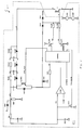
- FIG. 1 shows a circuit arrangement 1 with a drive circuit 2 and a power semiconductor switch S with controlled control terminal G (also referred to as gate), which allows VCE monitoring by means of a compensated voltage divider.
- the drive circuit 2 is used to drive the power semiconductor switch S.
- a voltage divider which is formed by the resistors RVCE1, RVCE2, RVCE3 and RME, is used to reduce the voltage occurring at the power terminal / collector C of the power semiconductor switch S high voltage to values, within the permissible input voltage range of the comparator COMP of the subsequent / downstream signal processing unit.
- the resistors RVCE1, RVCE2, RVCE3 are connected in series.
- the values of the resistors RVCE1, RVCE2, RVCE3 must typically be chosen very high in order to minimize the power loss within these resistors and thus the costs for the components and possibly required cooling measures.
- the parasitic input capacitance CAP can vary greatly in terms of process value.
- the parasitic input capacitance CAP can greatly depend on the layer structure, the manufacturer and the production lot.
- a compensated voltage divider can be used in which the resistors RVCE1, RVCE2, RVCE3, RME are assigned dominant capacitances CVCE1, CVCE2, CVCE3, CME (cf. FIG. 1 ).
- the disadvantage here is an additionally required space requirement, a reduction of the maximum permissible operating temperature, an increased number of components, increased costs and usually a reduced reliability.
- a further disadvantage of the use of such a compensated voltage divider is that, in the case of a monolithic integration of the comparator COMP and the control unit CONTROL of the signal processing unit, a setting of a blanking time in which the VCE monitoring is deactivated corresponds to the comparison of the measured collector and comparator COMP. emitter voltage must be followed by the setpoint, so must be performed within or by means of the control unit CONTROL.
- this requires additional measures for adjusting the blanking time, such as digital programming or other connection pins on the monolithically integrated signal processing unit.
- the mentioned disadvantages of the compensated voltage divider can be avoided by compensating the aforementioned voltage divider RVCE1, RVCE2, RVCE3, RME not by dominant capacitances, but instead by accepting in parallel the input capacitance of the signal processing unit following the power semiconductor switch S by connecting a (dominant) response time capacitance CA in parallel the parasitic input capacitance CAP is increased such that the necessary for the realization of the blanking time of the VCE monitoring time constant of the drive circuit results.
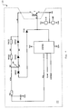
- the response time capacitance CA is typically associated with a response time resistor RA. This is in FIG. 2 which shows a circuit arrangement 1 'with a drive circuit 2' and a power semiconductor switch S, with which VCE monitoring can be performed.
- the response time capacitance CA is discharged by means of the control unit CONTROL via a switch M_D to a lower potential in the form of a predetermined reference potential Com or vee of the drive circuit 2 '.
- the response time capacitance CA is then charged via the resistor network RVCE1, RVCE2, RVCE3 connected to the collector C of the power semiconductor switch S.
- a decrease in the collector-emitter voltage leads to a reduction of the response time proportional to the reduction. This may result in an unintentional limitation on the optimal design of the power semiconductor switch S lead, although at the in FIG. 2 illustrated circuit arrangement 1 ', the short-circuit energy can be kept substantially constant.
- VCM_MAX a maximum value
- VCM_MAX a voltage divider formed by the resistors RVCE1, RVCE2, RVCE3, RME acts linearly.
- the output voltage of this voltage divider is limited by the diode DGH to the maximum value VCM_MAX.
- VCM_MAX can for example be derived from the operating / supply voltage Viso or from a voltage connected in the drive circuit 2 'by the control unit CONTROL voltage for the control terminal G of the power semiconductor switch.
- the switched voltage may be the output voltage at the output GH of an output stage M_ON responsible for the switched-on state of the power semiconductor switch S.
- Control unit CONTROL act The voltage VCM at the midpoint of the voltage divider RVCE1, RVCE2, RVCE3, RME is limited to this maximum value VCM_MAX, as long as the collector-emitter voltage is greater than a predetermined limit VCE_MIN. For collector-emitter voltages which are below the limit VCE_MIN, however, the voltage at the center VCM of the voltage divider RVCE1, RVCE2, RVCE3, RME is less than the maximum value VCM_MAX, so that also in this case the response time is extended accordingly.
- VCM_MAX the maximum value at the center VCM of the voltage divider RVCE1, RVCE2, RVCE3, RME is less than the maximum value VCM_MAX, so that also in this case the response time is extended accordingly.
- the response time capacitance CA and the response time resistor RA are kept constant in a wide range of collector-emitter voltage. This is achieved by minimizing the quotient or factor VCE_MIN / VCM_MAX from the above-defined value VCM_MAX and the predetermined minimum collector-emitter voltage VCE_MIN.
- a minimization of the factor VCE_MIN / VCM_MAX can be achieved, for example, by increasing the current flowing to the center VCM of the resistor network formed by the resistors RVCE1, RVCE2, RVCE3, RME, for example by increasing the resistance values of the collector C of the power semiconductor switch S connected resistor network RVCE1, RVCE2, RVCE3 are reduced.
- this measure is in contradiction to the fact that, as mentioned above, the values of the resistors RVCE1, RVCE2, RVCE3 of the resistor network connected in series with the collector C should be selected to be very high, in order to minimize the power loss caused by a high collector-emitter voltage Resistors RVCE1, RVCE2, RVCE3 and thus to keep the costs for the components and any necessary cooling measures as low as possible.
- the VCE_MIN / VCM_MAX factor may be minimized by decreasing the current flowing from the center VCM of the resistor network formed by resistors RVCE1, RVCE2, RVCE3, RME, for example by increasing the value of the response time RA.
- the value of the resistor RME of the voltage divider could also be increased.
- the resistor RME omitted, since the input voltage for the comparator COMP is already limited by the diode DGH.
- these measures would mean that, for a given response time, the value for the response time capacitance CA would have to be correspondingly reduced, which would result in the response time being influenced more strongly by the parasitic and process-dependent capacitance CAP.
- the parasitic effects are typically so dominant that it is difficult to realize a series-compatible matching of the response time of the circuit arrangement, in particular with regard to process control and thermal loading of the components , in particular for IGBT voltage classes from 3300 V to 6500 V.
- an overvoltage possibly occurring when the power semiconductor switch S is switched off is switched off with the aid of series-connected semiconductor components DZCE0, DZCE1, DZCE2, DZCE3 (for example zener diodes, avalanche diodes (see http://de.wikipedia.org / wiki / avalanche diode) and / or transient voltage suppressor diodes (see http://de.wikipedia.org/wiki/Suppressordiode) that are operated when overwriting a particular collector-emitter voltage in the breakdown, thereby limits that the power semiconductor switch S is turned on again, wherein the potential at the control terminal G of the power semiconductor switch S is temporarily raised approximately to the level of the supply / supply voltage Viso.
- DZCE0, DZCE1, DZCE2, DZCE3 for example zener diodes, avalanche diodes (see http://de.wikipedia.org / wiki / avalanche diode) and / or transient voltage suppressor diodes (see
- control connection line also called gate line
- CONTROL also called gate driver
- the control input ACL is preferably a low-impedance input of a current mirror circuit, the output current being available at the output GL of an output stage M_OFF of the control unit CONTROL being available at the output GL for the switched-off state or switch-off operation of the power semiconductor switch S being reduced as a function of the current flowing into the control input ACL.
- a semiconductor component DZCE0 of the series-connected, breakthrough-operated semiconductor components DZCE0, DZCE1, DZCE2, DZCE3 is bridged for a certain time during the turn-off operation of the power semiconductor switch S.
- the aim of the dynamic active clamping function is on the one hand to increase the sum of the breakdown voltages in the off state of the power semiconductor switch S and on the other hand, to reduce the sum of the breakdown voltages during the actual turn-off, so that the performance of the power semiconductor switch S can be better utilized without its leave safe working area.
- a semiconductor component DZCE0 or a part of the series-connected semiconductor components DZCE0, DZCE1, DZCE2, DZCE3 operated in the breakdown when a specific collector-emitter voltage is exceeded is bypassed during the switch-off operation of the power semiconductor switch S for a certain time.
- the bridging takes place by means of a switch M_DAAC, which is controlled via a control connection CTRL_DAAC by the control unit CONTROL.
- control unit CONTROL must at the same time ensure that the switch M_DAAC remains safely switched on in order not to unintentionally increase the nominal value for the permissible overvoltage during the switch-off operation of the power semiconductor switch.
- the potential at the control terminal CTRL_DAAC of the switch M_DAAC is higher than the potential at the control terminal G of the power semiconductor switch S and also higher than the level of the supply voltage Viso.
- This usually requires the use of relatively complex so-called charge pump (charge pump) or bootstrap feeders. Due to the high charge at the control terminal of the switch M_DAAC, however, results in a relatively high load on the supply, especially when the power semiconductor switch S is operated at higher switching frequencies.
- the drive circuit according to the invention for driving a power semiconductor switch has a signal processing unit for generating a control connection signal for a control connection (also called a gate) of a power semiconductor switch.
- the drive circuit comprises a resistor series circuit, which is connectable to a power supply serving as a power supply, which is also referred to as a collector, the power semiconductor switch and whose output is connected - at least indirectly - with a first input of the signal processing unit.
- the signal processing unit has a second input for a reference voltage for the collector-emitter voltage of the power semiconductor switch.
- the drive circuit comprises at least one semiconductor component, which is designed such that it is operated when a specific, predetermined collector-emitter voltage of the power semiconductor switch in breakthrough is exceeded.
- An output of the at least one semiconductor device is connected via a conductive connection to one between the resistors of the resistor series circuit or to the output of the resistor series circuit connected to the signal processing unit.
- the conductive connection preferably has no electronic components.
- the breakdown voltage of the at least one semiconductor component is selected such that the potential at the output of the at least one semiconductor component which is connected to the conductive connection, greater than the potential at the control terminal of the power semiconductor switch in the on state of the power semiconductor switch, in particular greater than 100 V.
- the potential at this output of the at least one semiconductor component preferably corresponds its breakdown voltage, which is preferably greater than 100V.
- a response time network which comprises at least one response time resistor, via which the collector remote output of the resistor series circuit is connected to the first input of the signal processing unit, wherein the response time of the drive circuit on the time constant of the response time network depends.
- the signal processing unit determines from the signal applied to its first input and from the reference voltage for the collector-emitter voltage of the power semiconductor switch a control connection signal for the control connection of the power semiconductor switch.
- the at least one semiconductor component is then operated in the breakdown and the potential at the output of the resistor series connection connected to the conductive connection or between the resistors of the resistor connected to the conductive connection Series connection is limited to a value which is greater than the potential at the control terminal of the power semiconductor switch in the on state of the power semiconductor switch and which is preferably greater than 100 V.
- the potential at the output of the series resistor connection connected to the conductive connection or at the terminal connected to the conductive connection between the resistors of the series resistance circuit preferably corresponds to the breakdown voltage of the at least one semiconductor component.
- the signal applied to the first input of the signal processing unit is derived from the potential at the collector of the power semiconductor conductor and is generated of the control terminal signal for the control terminal of the signal processing unit compared with the reference voltage.
- the drive circuit according to the invention and the method according to the invention are suitable both for switching on a power semiconductor switch in the short circuit (so-called short-circuit of type 1) and for the case of a short circuit in the switched-on state of the semiconductor switch (so-called short-circuit of type 2).
- the drive circuit according to the invention has a plurality of semiconductor components connected in series, which are operated in breakthrough when the predetermined, predetermined collector-emitter voltage for the power semiconductor switch is exceeded and of which the above, at least one semiconductor component is one.
- the signal processing unit preferably raises the instantaneous value of the control connection signal for the control connection of the power semiconductor switch.
- the power semiconductor switch which can be controlled or operated by the drive circuit according to the invention and the method according to the invention can, for example, be part of a switch module, in particular a half-bridge branch of an inverter, for traction / traction, for industrial electric drives, for solar energy, for wind energy, for high-voltage direct current transmission and / or for a flexible three-phase transmission system (FACTS).
- the power semiconductor switch may be a bipolar transistor (BJT), a gate-integrated bipolar transistor (IGBT), a metal-oxide-semiconductor field effect transistor (MOSFET), or a combination of these devices.
- FIGS. 1 to 3 have already been described in the introduction to the description and reference is made to this.
- FIG. 4 shows a circuit arrangement 10 with an exemplary drive circuit 20 and a power semiconductor switch S.
- the drive circuit 20 has a signal processing unit CONTROL, which has a first input for a voltage derived from a collector-emitter voltage of the power semiconductor switch S voltage VCA and a second input for a reference voltage VC -REF.
- the signal processing unit CONTROL comprises a comparator which compares the voltage VCA with the reference voltage VC-REF to form a comparison value.
- the signal processing unit CONTROL further comprises a control unit which, depending on the comparison value, outputs a control connection signal via a control output to the control connection G of the power semiconductor switch S.
- the comparator and the control unit are in the in FIG. 4 illustrated embodiment integrates shown as a signal processing unit CONTROL.
- the drive circuit 20 further comprises a resistor series circuit of the resistors RVCE2 and RVCE3, which is connected to the collector C of the power semiconductor switch S and the collector remote output to the potential VCM preferably via a from a response time RA and from a associated, with a reference potential Com connected response time capacitance CA response time network formed with the first input of the signal processing unit CONTROL is connected to which the voltage or the potential VCA is applied.
- the resistor series connection is used for VCE monitoring.
- the drive circuit 20 includes a series circuit of semiconductor devices DZCE1, DZCE2, DZCE3, which are designed such that they switch at a certain, predetermined collector-emitter voltage of the power semiconductor switch S in the breakthrough.
- the semiconductor components DZCE1, DZCE2, DZCE3 are in particular Zener diodes, avalanche diodes and / or transient voltage suppressor diodes.
- the semiconductor device series circuit is connected on the cathode side to the collector C of the power semiconductor switch S. On the anode side, the semiconductor component series circuit, for example via a diode D102 arranged in the opposite direction, is connected to the control output of the signal processing unit CONTROL.
- the semiconductor component series connection implements a dynamic active clamping function, wherein when the breakdown voltages of the semiconductor components DZCE1, DZCE2, DZCE3 are exceeded, the signal processing unit CONTROL preferably raises the control terminal signal for the control terminal G of the power semiconductor switch S or its (instantaneous) value ,
- a terminal 300 between two semiconductor devices DZCE1, DZCE2 is connected via a conductive connection 100 to the collector remote output 200 of the series resistance circuit.
- the potential at the output 200 of the series resistance circuit by means of the conductive connection 100 at least temporarily, namely for the time of breakthrough of the semiconductor device DZCE1, kept constant and thus stabilized, since it is limited to a value by the in The semiconductor device DZCE1, which is operated by breakdown, is determined in particular by its breakdown voltage of the semiconductor device DZCE1 preferably greater than 100 V.
- FIG. 5 shows a circuit arrangement 11 with a first embodiment of a drive circuit 21 and a power semiconductor switch S, wherein the comparator COMP and the control unit CONTROL of the signal processing unit are designed separately and the control unit CONTROL two output stages M_ON and M_OFF are assigned, each with the control terminal G of the power semiconductor switch S. connectable or connected.
- the power semiconductor switch S is switched on by the control unit CONTROL via the output stage M_ON and operated in the switched-on state. About the output stage M_OFF the power semiconductor switch S is turned off by the control unit CONTROL or operated in the off state.
- the resistor series circuit has three resistors RVCE1, RVCE2, RVCE3.
- the series connection of semiconductor components which are operated in breakthrough when a certain, predetermined collector-emitter voltage is exceeded, has four semiconductor components DZCE0, DZCE1, DZCE2, DZCE3.
- the semiconductor device element DZCE0 preferably likewise has a breakdown voltage of more than 100 V and can likewise be embodied as a Zener diode, as an avalanche diode or as a transient voltage suppressor diode.
- the terminal 300 between the two semiconductor devices DZCE1 and DZCE2 is connected via the conductive connection 100 to a terminal 200 between the resistors RVCE1 and RVCE2, ie, the first intermediate terminal 200 of the series resistance circuit, which is on a first Intermediate potential is.
- This intermediate potential is kept constant by means of the conductive connection 100 at least temporarily, namely for the time of breakdown of the semiconductor device DZCE1, and thus stabilized by being limited to a value determined by the breakdown semiconductor device DZCE1, in particular by its breakdown voltage, which is preferably greater than 100V.
- control unit CONTROL When the breakdown voltages of the semiconductor components DZCE0, DZCE1, DZCE2, DZCE3 are exceeded, the control unit CONTROL preferably raises the control terminal signal for the control terminal G of the power semiconductor switch S or its (instantaneous) value.
- the advantage of stabilizing the potential at the intermediate terminal or output 200 of the series resistor circuit is that the undesired influence of parasitic capacitances CP assigned to the resistors RVCE1, RVCE2, RVCE3 of the series resistance circuit (cf. FIG. 5 ), to the response time is reduced.
- Another advantage is that the amount of components compared to in FIG. 3
- the stabilized potential at the intermediate connection or the output 200 of the resistance series circuit is advantageously greater than the supply or supply voltage available in the drive circuit, in particular as the control connection signal or the Potential at the control terminal G in the on state of the power semiconductor switch S and as the potential Viso a voltage source V-ON for feeding the output stage M_ON for the on or on state of the power semiconductor switch S.
- One or more further conductive connections can be provided, each connecting a collector-side output 301 of one of the further semiconductor components DZCE2 of the semiconductor component series circuit to a further intermediate connection 201 of the resistance series circuit.
- a switch M_DAAC whose control terminal CTRL_DAAC is directly or indirectly connected to an output of the signal processing unit or the control unit CONTROL is preferably arranged indirectly or directly parallel to the collector-distal semiconductor component DZCE0 of the semiconductor component series circuit.
- the drive circuit 21 is now designed such that the signal processing unit or the control unit CONTROL preferably switches the switch M_DAAC in the switched-on state of the power semiconductor switch S and preferably at the beginning of the turn-off operation of the power semiconductor switch S.
- the semiconductor device DZCE0 is bridged, and the voltage across the semiconductor device DZCE0 and thus the sum of the voltages across the semiconductor devices DZCE0, DZCE1, DZCE2, DZCE3 is reduced when the semiconductor devices DZCE0, DZCE1, DZCE2, DZCE3 during the shutdown of the power semiconductor switch S in Breakthrough are operated.
- Advantage of the stabilization of the potential at the intermediate terminal or output 200 of the series resistance circuit is also that an undesirable charge transfer during the switching of the switch M_DAAC to realize the dynamic active clamping function between the parasitic capacitances CP and the response time capacity CA reduced can be, which further simplifies the keeping constant of the response time in a wide range of collector-emitter voltage even further.
- the semiconductor device DZCE1 connected to the conductive interconnect 100 is an active part of a semiconductor device series circuit for realizing an active clamping function, as in FIGS FIGS. 4 and 5 (and also in FIG. 7 ), the supply of the semiconductor device DZCE1 from the collector C of the power semiconductor switch S via the conductive connection 100 and the resistor series circuit for the realization of the VCE monitoring, so advantageously no additional auxiliary power supply of the semiconductor device DZCE1 is required whose potential is the supply voltage of the inventive Drive circuit exceeds.
- the voltage VCA at the first input of the signal processing unit or the comparator COMP and / or the voltage VCM at the collector-remote output of the resistor series circuit should be limited to values that can be processed by the subsequent signal processing unit or the subsequent comparator COMP.
- the anode of a diode DGH to the collector remote output of the resistor series circuit (see. FIG. 5 ) or alternatively connected to the first input of the signal processing unit or the comparator COMP, wherein the cathode of the diode DGH is connected to the control terminal G of the power semiconductor switch S or can be connected.
- the diode can advantageously be monolithic, ie be executed within the signal processing unit or the comparator COMP.
- one or more semiconductor components operated in the breakdown for example Zener diodes, avalanche diodes and / or transient voltage suppressor diodes, can be connected to the collector-remote output of the resistor series circuit or to the first one analogously to the diode DGH Input of the signal processing unit or the comparator COMP are connected.
- FIG. 6 shows a circuit arrangement 12 with a drive circuit 22 and a power semiconductor switch S.
- a semiconductor device DZCE1 provided, which is operated at a certain, predetermined collector-emitter voltage in the breakthrough and thus at least temporarily constant potential and which is for example a single zener diode, avalanche diode or transient Voltage suppressor diode acts.
- the breakdown voltage of the semiconductor device DZCE1 is preferably greater than 100 V.
- the cathode-side output 300 of the semiconductor device DZCE1 is connected via the conductive connection 100 with the intermediate terminal 200 between the resistors RVCE1 and RVCE2 of the resistor series circuit, so that the intermediate potential at the intermediate terminal 200 at the exceeded predetermined collector-emitter voltage is stabilized by the potential at the cathode-side output 300 of the semiconductor device DZCE1.
- FIG. 5 shown further semiconductor devices DZCE0, DZCE2, DZCE3 and the wiring with the controlled via the control unit CONTROL switch M_DAAC for realizing an active clamping function are in FIG. 6 eliminated
- FIG. 7 shows a circuit arrangement 13 with a second embodiment of an inventive driving circuit 23 and a power semiconductor switch S.
- a signal-processing frequency and / or time-dependent impedance which is arranged between the resistor series circuit and the response time network RA, CA and parallel to the response time network RA, CA and whose input at the potential VCM am Output of the resistor series circuit and the output of a reference potential Com or vee of the drive circuit 23 is located.
- the frequency and / or time dependent impedance preferably comprises as in FIG.
- a diode D107 may be provided, whose anode is connected between the resistor RME_D and the capacitor CME_D and whose cathode is connected to the output of the response time network RA, CA or to the first input of the signal processing unit or of the comparator COMP.
- the diode D107 is used to accelerate the discharge of the capacitance CME_D, to ensure a safe start condition / a safe start condition for the capacity CME_D even with short turn-off of the power semiconductor switch S.
- the dynamic VCE monitoring serves to temporarily reduce the measured value VCM of the collector-emitter voltage for advantageous compensation of the time course of the collector-emitter voltage when turning on the power semiconductor switch S.
- FIG. 7 in comparison with the Figures 5 and 6 a drive circuit 23 according to the invention with a detailed wiring of the switch M_DAAC, which is turned on by the signal processing unit or the control unit CONTROL in the on state and at the beginning of the shutdown state of the power semiconductor switch S for bridging the semiconductor device DZCE0 to realize a dynamic active clamping function.
- the switch M_DAAC is turned off.
- the switch M_DAAC For driving the switch M_DAAC is preferably its control terminal CTRL_DAAC via a drive network 30, in particular of two series-connected resistors R111 and R101, a diode D108 and a Zener diode DZ5 (or an avalanche diode or a transient voltage suppressor Diode), with the control terminal G or the output GH (see above in FIG FIG. 7 shown) of the responsible for the on state of the power semiconductor switch S output stage M_ON the signal processing unit or control unit CONTROL connected.
- a drive network 30 in particular of two series-connected resistors R111 and R101, a diode D108 and a Zener diode DZ5 (or an avalanche diode or a transient voltage suppressor Diode), with the control terminal G or the output GH (see above in FIG FIG. 7 shown) of the responsible for the on state of the power semiconductor switch S output stage M_ON the signal processing unit or control unit CONTROL connected.
- a signal derived from the profile of the potential at the output GH, the potential at the control terminal G or a switching command COMMAND for the signal processing unit or the control unit CONTROL forms the input signal for the control network 30 upstream of the switch M_DAAC, ie the control signal for the switch M_DAAC.
- the power or control terminal charge (gate charge) for operating the switch M_DAAC is thus obtained directly from the regular control connection G or the output GH of the output stage M_ON responsible for the switched-on state of the power semiconductor switch S or a signal derived therefrom. This can advantageously on an additional, relatively complex so-called charge pump or bootstrap supply of the switch M_DAAC be waived.
- the diode D108 and the Zener diode DZ5 are connected to one another on the anode side and connected in parallel to the resistor R111.
- a parallel circuit of a resistor R112 and a capacitor C106 is preferably provided, which is connected to the control terminal of the switch M_DAAC and to its power connection for current discharge.
- the resistor R111 of the drive network 30 the capacitance C106 and the input capacitance of the switch M_DAAC, the switch-off operation of the switch M_DAAC with respect to the input signal of the drive network 30, ie the actuating signal which is in FIG. 7 is exemplified by the potential at the output GH of the output stage M_ON delayed so that during the turn-off of the power semiconductor switch S, the switch M_DAAC remains turned on and fully opens only in the off state of the power semiconductor switch S.
- the diode D108 is used to accelerate the turn-on of the switch M_DAAC, so that even with short turn-on of the power semiconductor switch S is ensured that the switch M_DAAC is safely turned on during subsequent shutdown operations of the power semiconductor switch S.
- the control signal for the switch M_DAAC is correspondingly reduced in its safe working range.
- the resistor R101 serves to reduce a peak current load on the control terminal CTRL_DAAC of the switch M_DAAC and thus reduce a peak current load on the output GH of the output stage M_ON (which peak current load could lead to less current at the control terminal G of the power semiconductor switch S), so that the total current capability of the drive circuit 23 for head for and operation of the power semiconductor switch S is available.
- the semiconductor device DZCE0 and the switch M_DAAC preferably a resistor RSYM connected in parallel, which serves to stabilize the output voltage of the switch M_DAAC in case of larger leakage currents of the semiconductor device DZCE1 or in the case of leakage currents of the semiconductor device DZCE0, which are smaller than leakage currents of the semiconductor device DZCE1 ,
- a resistor RSYM connected in parallel, which serves to stabilize the output voltage of the switch M_DAAC in case of larger leakage currents of the semiconductor device DZCE1 or in the case of leakage currents of the semiconductor device DZCE0, which are smaller than leakage currents of the semiconductor device DZCE1 .
Landscapes
- Electronic Switches (AREA)
- Power Conversion In General (AREA)
Claims (11)
- Circuit de commande destiné à commander un commutateur de puissance à semi-conducteur (S) comportant une unité de traitement du signal (CONTROL) destinée à générer un signal de connexion de commande pour une connexion de commande (G) du commutateur de puissance à semi-conducteur (S), dans lequel le circuit de commande (20 ; 21 ; 22 ; 23) comprend un circuit série de résistances (RCVE1, RCVE2, RCVE3) qui est connecté à une borne de puissance (C) servant à l'alimentation en courant du commutateur de puissance à semi-conducteur (S) et dont la sortie est reliée à une première entrée de l'unité de traitement du signal (CONTROL), et dans lequel l'unité de traitement du signal (CONTROL) présente une seconde entrée destinée à une tension de référence (VC-REF) pour la tension collecteur-émetteur du commutateur de puissance à semi-conducteur (S), caractérisé en ce qu'il est prévu au moins un composant à semi-conducteur (DZCE1, DZCE2, DZCE3) qui est conçu de manière à être attaqué en mode claquage lors du dépassement d'une tension collecteur-émetteur spécifique du commutateur de puissance à semi-conducteur (S), dans lequel une sortie (300) de l'au moins un composant à semi-conducteur (DZCE1, DZCE2, DZCE3) est reliée par l'intermédiaire d'une liaison conductrice (100) à une borne (200) située entre les résistances (RCVE1, RCVE2, RCVE3) du circuit série de résistances ou à la sortie (200) du circuit série de résistances qui est relié à l'unité de traitement du signal (CONTROL), dans lequel il est prévu un autre composant à semi-conducteur (DZCE0) qui est connecté à l'au moins un premier composant à semi-conducteur (DZCE1, DZCE2, DZCE3), dans lequel un commutateur (M_DAAC) est disposé en parallèle à cet autre composant à semi-conducteur (DZCE0) dont la borne de commande (CTRL_DAAC) est directement ou indirectement reliée à une sortie de l'unité de traitement du signal (CONTROL), à laquelle est reliée la borne de commande (G) du commutateur de puissance à semi-conducteur (S), dans lequel le circuit de commande (21 ; 23) est conçu de telle manière que l'unité de traitement du signal (CONTROL) rende passant le commutateur (M_DAAC) à l'état passant du commutateur de puissance à semi-conducteur (S) et/ou au début du processus de passage à l'état passant du commutateur de puissance à semi-conducteur (S), et dans lequel la tension de claquage de l'au moins un composant à semi-conducteur (DZCE1, DZCE2, DZCE3) est sélectionnée de manière à ce que le potentiel à la sortie (300) de l'au moins un composant à semi-conducteur (DZCE1, DZCE2, DZCE3) soit supérieur au potentiel sur la borne de commande (G) du commutateur de puissance à semi-conducteur (S) à l'état passant du commutateur de puissance à semi-conducteur (S).
- Circuit de commande selon la revendication 1, caractérisé en ce que le potentiel sur la sortie (300) de l'au moins un composant à semi-conducteur (DZCE1, DZCE2, DZCE3), notamment la tension de claquage de l'au moins un composant à semi-conducteur (DZCE1, DZCE2, DZCE3), est supérieur à 100 V.
- Circuit de commande selon la revendication 1 ou 2, caractérisé en ce que l'au moins un composant à semi-conducteur est une diode Zener, une diode à avalanche et/ou une diode de suppression de tension transitoire.
- Circuit de commande selon l'une quelconque des revendications précédentes, caractérisé en ce qu'il est prévu une pluralité de composants à semi-conducteur (DZCE1, DZCE2, DZCE3) qui sont connectés en série.
- Circuit de commande selon la revendication 4, caractérisé en ce qu'il est prévu au moins une autre liaison conductrice qui relie une sortie (301) de l'un des autres composants à semi-conducteur (DZCE2, DZCE3) à une autre borne (201) située entre les résistances (RCVE1, RCVE2, RCVE3) du circuit série de résistances.
- Circuit de commande selon l'une quelconque des revendications précédentes, caractérisé en ce que la sortie du circuit série de résistances (RCVE1, RCVE2, RCVE3) est reliée par l'intermédiaire d'un réseau de temps de réponse (RA, CA) à la première entrée de l'unité de traitement du signal (CONTROL), le réseau de temps de réponse comprenant une résistance de temps de réponse (RA).
- Circuit de commande selon la revendication 6, caractérisé en ce que, entre le circuit série de résistances (RCVE1, RCVE2, RCVE3) et le réseau de temps de réponse (RA, CA), il est prévu en parallèle au réseau de temps de réponse (RA, CA), une impédance dépendant de la fréquence et/ou du temps (RME_D, CME_D), qui comprend notamment un circuit série d'une résistance (RME_D) et d'une capacité (CME_D) ou le circuit série d'une résistance et d'un commutateur commandé par l'unité de traitement du signal (CONTROL).
- Procédé de commande d'un commutateur de puissance à semi-conducteur (S) comportant un circuit de commande (20 ; 21 ; 22 ; 23) selon l'une quelconque des revendications précédentes, dans lequel l'unité de traitement du signal (CONTROL) détermine à partir du signal (VCA) présent sur sa première entrée, et de la tension de référence (VC-REF) destinée à la tension collecteur-émetteur du commutateur de puissance à semi-conducteur (S), un signal de connexion de commande destiné à la connexion de commande (G) du commutateur de puissance à semi-conducteur (S), caractérisé en ce que, lors du dépassement d'une tension collecteur-émetteur déterminée, l'au moins un composant à semi-conducteur (DZCE0, DZCE1, DZCE2, DZCE3) est attaqué en mode claquage et en ce que le potentiel sur la sortie (200) reliée par la liaison conductrice (100) du circuit série de résistances (RVCE1, RVCE2, RVCE3) ou sur la borne (200) reliée par la liaison conductrice (100) située entre les résistances (RVCE1, RVCE2, RVCE3) du circuit série de résistances, est limité à une valeur qui est supérieure au potentiel sur la borne de commande (G) du commutateur de puissance à semi-conducteur (S) à l'état passant du commutateur de puissance à semi-conducteur (S), dans lequel, à l'état passant du commutateur de puissance à semi-conducteur (S) et/ou au début du processus de passage à l'état non passant du commutateur de puissance à semi-conducteur (S), la tension aux bornes d'un autre composant à semi-conducteur (DZCE0) qui est connecté en série à l'au moins un composant à semi-conducteur (DZCE1, DZCE2, DZCE3), est réduite au moyen d'un commutateur (M_DAAC) disposé en parallèle à cet autre composant à semi-conducteur (DZCE0) lorsque les composants à semi-conducteur (DZCE1, DZCE2, DZCE3) sont attaqués en mode claquage.
- Procédé selon la revendication 8, caractérisé en ce que le potentiel sur la sortie (200) reliée par la liaison conductrice (100) du circuit série de résistances (RVCE1, RVCE2, RVCE3) ou à la borne (200) reliée par la liaison conductrice (100) située entre les résistances (RVCE1, RVCE2, RVCE3) du circuit série de résistances est limité à une valeur supérieure à 100 V.
- Procédé selon la revendication 8 ou 9, caractérisé en ce que, lors du dépassement de la tension de claquage de l'au moins un composant à semi-conducteur (DZCE0, DZCE1, DZCE2, DZCE3), l'unité de traitement du signal (CONTROL) augmente la valeur du signal de connexion de commande destiné à la connexion de commande (G) du commutateur de puissance à semi-conducteur (S).
- Procédé selon la revendication 8, caractérisé en ce que le signal de réglage destiné au commutateur (M_DAAC) disposé en parallèle à l'autre composant à semi-conducteur (DZCE0) est formé par le signal de connexion de commande destiné à la connexion de commande (G) du commutateur de puissance à semi-conducteur (S) ou est dérivé de celui-ci ou est dérivé d'un ordre de commutation (COMMAND) destiné à l'unité de traitement du signal (CONTROL).
Priority Applications (4)
| Application Number | Priority Date | Filing Date | Title |
|---|---|---|---|
| EP13197268.9A EP2744110B1 (fr) | 2011-03-16 | 2011-03-16 | Circuit d'attaque et procédé destiné à la commande d'un circuit semi-conducteur de puissance |
| EP11002165.6A EP2501042B1 (fr) | 2011-03-16 | 2011-03-16 | Circuit d'attaque et procédé destiné à la commande d'un circuit semi-conducteur de puissance |
| JP2012053172A JP5944698B2 (ja) | 2011-03-16 | 2012-03-09 | パワー半導体スイッチの制御回路及びその制御方法 |
| US13/421,581 US8598921B2 (en) | 2006-11-22 | 2012-03-15 | Control circuit and method for controlling a power semiconductor switch |
Applications Claiming Priority (1)
| Application Number | Priority Date | Filing Date | Title |
|---|---|---|---|
| EP11002165.6A EP2501042B1 (fr) | 2011-03-16 | 2011-03-16 | Circuit d'attaque et procédé destiné à la commande d'un circuit semi-conducteur de puissance |
Related Child Applications (1)
| Application Number | Title | Priority Date | Filing Date |
|---|---|---|---|
| EP13197268.9A Division EP2744110B1 (fr) | 2011-03-16 | 2011-03-16 | Circuit d'attaque et procédé destiné à la commande d'un circuit semi-conducteur de puissance |
Publications (2)
| Publication Number | Publication Date |
|---|---|
| EP2501042A1 EP2501042A1 (fr) | 2012-09-19 |
| EP2501042B1 true EP2501042B1 (fr) | 2013-12-18 |
Family
ID=44352162
Family Applications (2)
| Application Number | Title | Priority Date | Filing Date |
|---|---|---|---|
| EP13197268.9A Active EP2744110B1 (fr) | 2011-03-16 | 2011-03-16 | Circuit d'attaque et procédé destiné à la commande d'un circuit semi-conducteur de puissance |
| EP11002165.6A Active EP2501042B1 (fr) | 2006-11-22 | 2011-03-16 | Circuit d'attaque et procédé destiné à la commande d'un circuit semi-conducteur de puissance |
Family Applications Before (1)
| Application Number | Title | Priority Date | Filing Date |
|---|---|---|---|
| EP13197268.9A Active EP2744110B1 (fr) | 2011-03-16 | 2011-03-16 | Circuit d'attaque et procédé destiné à la commande d'un circuit semi-conducteur de puissance |
Country Status (2)
| Country | Link |
|---|---|
| EP (2) | EP2744110B1 (fr) |
| JP (1) | JP5944698B2 (fr) |
Families Citing this family (7)
| Publication number | Priority date | Publication date | Assignee | Title |
|---|---|---|---|---|
| EP2884662B1 (fr) * | 2013-12-13 | 2019-06-26 | Power Integrations Switzerland GmbH | Dispositifs et procédé de détection d'un état de court-circuit ou de surtension dans un commutateur de puissance à semi-conducteurs |
| DE102016207384A1 (de) * | 2016-04-29 | 2017-11-02 | Robert Bosch Gmbh | Verfahren zum Schutz eines Halbleiterschalters, Schutzvorrichtung für einen Halbleiterschalter und Ansteuerschaltung für einen Halbleiterschalter |
| DE102017002573B4 (de) | 2017-03-16 | 2019-07-04 | Infineon Technologies Ag | Überspannungsschutz |
| EP3595152B1 (fr) | 2018-07-12 | 2023-09-06 | Power Integrations, Inc. | Protection de commutateurs à semi-conducteurs dans des convertisseurs de puissance à mode commuté |
| US10897250B2 (en) * | 2018-11-16 | 2021-01-19 | Transportation Ip Holdings, Llc | Systems and methods for controlling dynamic avalanche in switching devices |
| JP7331480B2 (ja) * | 2019-06-17 | 2023-08-23 | 株式会社デンソー | 信号検出回路 |
| WO2021152734A1 (fr) * | 2020-01-29 | 2021-08-05 | 三菱電機株式会社 | Circuit de détection de surintensité et dispositif de conversion de puissance |
Family Cites Families (10)
| Publication number | Priority date | Publication date | Assignee | Title |
|---|---|---|---|---|
| DE3104015C2 (de) | 1981-02-05 | 1984-10-11 | Siemens AG, 1000 Berlin und 8000 München | Überstromschutzanordnung für einen Halbleiterschalter |
| DE3243467C2 (de) * | 1982-11-24 | 1986-02-20 | Siemens AG, 1000 Berlin und 8000 München | Einrichtung zum Schutz eines Schalttransistors |
| DE3689445T2 (de) * | 1985-02-08 | 1994-07-14 | Toshiba Kawasaki Kk | Schutzschaltung für einen Bipolartransistor mit isoliertem Gate. |
| FR2693853B1 (fr) * | 1992-07-16 | 1994-10-21 | Sgs Thomson Microelectronics | Circuit de protection d'un composant de puissance contre des surtensions directes. |
| US5444591A (en) * | 1993-04-01 | 1995-08-22 | International Rectifier Corporation | IGBT fault current limiting circuit |
| JP2002151989A (ja) * | 2000-11-14 | 2002-05-24 | Toyota Industries Corp | クランプ回路 |
| JP2002368593A (ja) * | 2001-06-05 | 2002-12-20 | Denso Corp | 半導体回路 |
| JP3666475B2 (ja) * | 2002-06-25 | 2005-06-29 | 日産自動車株式会社 | アクティブクランプ回路 |
| JP2009253484A (ja) * | 2008-04-03 | 2009-10-29 | Fuji Electric Systems Co Ltd | 電力変換装置 |
| JP4912444B2 (ja) * | 2009-08-10 | 2012-04-11 | 三菱電機株式会社 | 半導体装置 |
-
2011
- 2011-03-16 EP EP13197268.9A patent/EP2744110B1/fr active Active
- 2011-03-16 EP EP11002165.6A patent/EP2501042B1/fr active Active
-
2012
- 2012-03-09 JP JP2012053172A patent/JP5944698B2/ja active Active
Also Published As
| Publication number | Publication date |
|---|---|
| JP2012195937A (ja) | 2012-10-11 |
| JP5944698B2 (ja) | 2016-07-05 |
| EP2501042A1 (fr) | 2012-09-19 |
| EP2744110B1 (fr) | 2017-03-08 |
| EP2744110A1 (fr) | 2014-06-18 |
Similar Documents
| Publication | Publication Date | Title |
|---|---|---|
| EP2501042B1 (fr) | Circuit d'attaque et procédé destiné à la commande d'un circuit semi-conducteur de puissance | |
| DE102005045099B4 (de) | Entsättigungsschaltung mit einem IGBT | |
| DE102012207147B4 (de) | Verfahren zum Ansteuern von Leistungshalbleiterschaltern | |
| EP0561316B1 (fr) | Circuit de commande pour un commutateur semi-conducteur commandé en tension | |
| DE112013006487B4 (de) | Ansteuervorrichtung für Halbleiterelemente und Halbleitervorrichtigung | |
| DE102013002266B4 (de) | Bootstrap-Schaltungsanordnung für einen IGBT | |
| DE102012207155B4 (de) | Schaltungsanordnung zum Ansteuern eines Halbleiter-Schaltelements | |
| EP1728324B1 (fr) | Circuit de commande destine a la commande d'un circuit electronique de puissance et procede correspondant | |
| WO2015189332A1 (fr) | Dispositif et procédé pour générer un signal de référence dynamique pour un circuit de pilotage pour un disjoncteur de puissance à semi-conducteur | |
| DE102013105230A1 (de) | Treiberschaltkreis für einen Transistor | |
| EP0643485B1 (fr) | Montage servant au blocage doux d'un dispositif semi-conducteur FET lors d'un surcourant | |
| EP0690898B1 (fr) | Circuit de protection contre les surtensions pour un commutateur semiconducteur de puissance pouvant être mis en circuit ou hors circuit | |
| DE4012382C2 (fr) | ||
| AT523936B1 (de) | Verfahren und vorrichtung zum steuern eines halbleiterschalters | |
| EP3317967B1 (fr) | Circuit de commutation destiné à la commande d'un transistor | |
| DE102021101327A1 (de) | Gate-ansteuerungsvorrichtung, gate-ansteuerungsverfahren, leistungshalbleitermodul und stromwandlervorrichtung | |
| DE10333819A1 (de) | Gateansteuerungsschaltung in Leistungsmodulen | |
| DE10035388C2 (de) | Stromschaltanordnung | |
| EP3449571B1 (fr) | Procédé de protection d'un commutateur à semi-conducteur, dispositif de protection pour commutateur à semi-conducteur et circuit de commande d'un commutateur à semi-conducteur | |
| DE10035387B4 (de) | Stromschaltanordnung | |
| DE102015114284B3 (de) | Verfahren und ansteuerschaltung zum ansteuern eines transistors | |
| DE19717715C2 (de) | Verfahren zum Ansteuern eines feldgesteuerten Leistungshalbleiterschalters | |
| DE102018107474A1 (de) | Steuereinrichtung für einen Leistungshalbleiterschalter | |
| DE102022117363A1 (de) | Schutzschaltung zum Schutz eines Leistungsschalters gegen Kurzschluss und Überstrom | |
| DE10117356B4 (de) | Schaltungsanordnung |
Legal Events
| Date | Code | Title | Description |
|---|---|---|---|
| PUAI | Public reference made under article 153(3) epc to a published international application that has entered the european phase |
Free format text: ORIGINAL CODE: 0009012 |
|
| 17P | Request for examination filed |
Effective date: 20110916 |
|
| AK | Designated contracting states |
Kind code of ref document: A1 Designated state(s): AL AT BE BG CH CY CZ DE DK EE ES FI FR GB GR HR HU IE IS IT LI LT LU LV MC MK MT NL NO PL PT RO RS SE SI SK SM TR |
|
| AX | Request for extension of the european patent |
Extension state: BA ME |
|
| RIC1 | Information provided on ipc code assigned before grant |
Ipc: H03K 17/082 20060101AFI20130328BHEP |
|
| GRAP | Despatch of communication of intention to grant a patent |
Free format text: ORIGINAL CODE: EPIDOSNIGR1 |
|
| INTG | Intention to grant announced |
Effective date: 20130711 |
|
| RAP1 | Party data changed (applicant data changed or rights of an application transferred) |
Owner name: CT-CONCEPT HOLDING GMBH |
|
| GRAS | Grant fee paid |
Free format text: ORIGINAL CODE: EPIDOSNIGR3 |
|
| GRAA | (expected) grant |
Free format text: ORIGINAL CODE: 0009210 |
|
| AK | Designated contracting states |
Kind code of ref document: B1 Designated state(s): AL AT BE BG CH CY CZ DE DK EE ES FI FR GB GR HR HU IE IS IT LI LT LU LV MC MK MT NL NO PL PT RO RS SE SI SK SM TR |
|
| REG | Reference to a national code |
Ref country code: GB Ref legal event code: FG4D Free format text: NOT ENGLISH |
|
| REG | Reference to a national code |
Ref country code: CH Ref legal event code: EP |
|
| REG | Reference to a national code |
Ref country code: AT Ref legal event code: REF Ref document number: 645985 Country of ref document: AT Kind code of ref document: T Effective date: 20140115 |
|
| REG | Reference to a national code |
Ref country code: IE Ref legal event code: FG4D Free format text: LANGUAGE OF EP DOCUMENT: GERMAN |
|
| REG | Reference to a national code |
Ref country code: DE Ref legal event code: R096 Ref document number: 502011001811 Country of ref document: DE Effective date: 20140206 |
|
| REG | Reference to a national code |
Ref country code: NL Ref legal event code: T3 |
|
| PG25 | Lapsed in a contracting state [announced via postgrant information from national office to epo] |
Ref country code: NO Free format text: LAPSE BECAUSE OF FAILURE TO SUBMIT A TRANSLATION OF THE DESCRIPTION OR TO PAY THE FEE WITHIN THE PRESCRIBED TIME-LIMIT Effective date: 20140318 Ref country code: FI Free format text: LAPSE BECAUSE OF FAILURE TO SUBMIT A TRANSLATION OF THE DESCRIPTION OR TO PAY THE FEE WITHIN THE PRESCRIBED TIME-LIMIT Effective date: 20131218 Ref country code: LT Free format text: LAPSE BECAUSE OF FAILURE TO SUBMIT A TRANSLATION OF THE DESCRIPTION OR TO PAY THE FEE WITHIN THE PRESCRIBED TIME-LIMIT Effective date: 20131218 Ref country code: SE Free format text: LAPSE BECAUSE OF FAILURE TO SUBMIT A TRANSLATION OF THE DESCRIPTION OR TO PAY THE FEE WITHIN THE PRESCRIBED TIME-LIMIT Effective date: 20131218 Ref country code: HR Free format text: LAPSE BECAUSE OF FAILURE TO SUBMIT A TRANSLATION OF THE DESCRIPTION OR TO PAY THE FEE WITHIN THE PRESCRIBED TIME-LIMIT Effective date: 20131218 |
|
| REG | Reference to a national code |
Ref country code: LT Ref legal event code: MG4D |
|
| PG25 | Lapsed in a contracting state [announced via postgrant information from national office to epo] |
Ref country code: RS Free format text: LAPSE BECAUSE OF FAILURE TO SUBMIT A TRANSLATION OF THE DESCRIPTION OR TO PAY THE FEE WITHIN THE PRESCRIBED TIME-LIMIT Effective date: 20131218 Ref country code: LV Free format text: LAPSE BECAUSE OF FAILURE TO SUBMIT A TRANSLATION OF THE DESCRIPTION OR TO PAY THE FEE WITHIN THE PRESCRIBED TIME-LIMIT Effective date: 20131218 |
|
| PG25 | Lapsed in a contracting state [announced via postgrant information from national office to epo] |
Ref country code: EE Free format text: LAPSE BECAUSE OF FAILURE TO SUBMIT A TRANSLATION OF THE DESCRIPTION OR TO PAY THE FEE WITHIN THE PRESCRIBED TIME-LIMIT Effective date: 20131218 Ref country code: IS Free format text: LAPSE BECAUSE OF FAILURE TO SUBMIT A TRANSLATION OF THE DESCRIPTION OR TO PAY THE FEE WITHIN THE PRESCRIBED TIME-LIMIT Effective date: 20140418 |
|
| PG25 | Lapsed in a contracting state [announced via postgrant information from national office to epo] |
Ref country code: SK Free format text: LAPSE BECAUSE OF FAILURE TO SUBMIT A TRANSLATION OF THE DESCRIPTION OR TO PAY THE FEE WITHIN THE PRESCRIBED TIME-LIMIT Effective date: 20131218 Ref country code: RO Free format text: LAPSE BECAUSE OF FAILURE TO SUBMIT A TRANSLATION OF THE DESCRIPTION OR TO PAY THE FEE WITHIN THE PRESCRIBED TIME-LIMIT Effective date: 20131218 Ref country code: PT Free format text: LAPSE BECAUSE OF FAILURE TO SUBMIT A TRANSLATION OF THE DESCRIPTION OR TO PAY THE FEE WITHIN THE PRESCRIBED TIME-LIMIT Effective date: 20140418 Ref country code: CY Free format text: LAPSE BECAUSE OF FAILURE TO SUBMIT A TRANSLATION OF THE DESCRIPTION OR TO PAY THE FEE WITHIN THE PRESCRIBED TIME-LIMIT Effective date: 20131218 Ref country code: ES Free format text: LAPSE BECAUSE OF FAILURE TO SUBMIT A TRANSLATION OF THE DESCRIPTION OR TO PAY THE FEE WITHIN THE PRESCRIBED TIME-LIMIT Effective date: 20131218 Ref country code: PL Free format text: LAPSE BECAUSE OF FAILURE TO SUBMIT A TRANSLATION OF THE DESCRIPTION OR TO PAY THE FEE WITHIN THE PRESCRIBED TIME-LIMIT Effective date: 20131218 Ref country code: CZ Free format text: LAPSE BECAUSE OF FAILURE TO SUBMIT A TRANSLATION OF THE DESCRIPTION OR TO PAY THE FEE WITHIN THE PRESCRIBED TIME-LIMIT Effective date: 20131218 |
|
| REG | Reference to a national code |
Ref country code: DE Ref legal event code: R097 Ref document number: 502011001811 Country of ref document: DE |
|
| PLBE | No opposition filed within time limit |
Free format text: ORIGINAL CODE: 0009261 |
|
| STAA | Information on the status of an ep patent application or granted ep patent |
Free format text: STATUS: NO OPPOSITION FILED WITHIN TIME LIMIT |
|
| PG25 | Lapsed in a contracting state [announced via postgrant information from national office to epo] |
Ref country code: DK Free format text: LAPSE BECAUSE OF FAILURE TO SUBMIT A TRANSLATION OF THE DESCRIPTION OR TO PAY THE FEE WITHIN THE PRESCRIBED TIME-LIMIT Effective date: 20131218 Ref country code: LU Free format text: LAPSE BECAUSE OF FAILURE TO SUBMIT A TRANSLATION OF THE DESCRIPTION OR TO PAY THE FEE WITHIN THE PRESCRIBED TIME-LIMIT Effective date: 20140316 |
|
| 26N | No opposition filed |
Effective date: 20140919 |
|
| REG | Reference to a national code |
Ref country code: IE Ref legal event code: MM4A Ref country code: DE Ref legal event code: R097 Ref document number: 502011001811 Country of ref document: DE Effective date: 20140919 |
|
| PG25 | Lapsed in a contracting state [announced via postgrant information from national office to epo] |
Ref country code: IE Free format text: LAPSE BECAUSE OF NON-PAYMENT OF DUE FEES Effective date: 20140316 |
|
| REG | Reference to a national code |
Ref country code: FR Ref legal event code: PLFP Year of fee payment: 5 |
|
| PG25 | Lapsed in a contracting state [announced via postgrant information from national office to epo] |
Ref country code: SI Free format text: LAPSE BECAUSE OF FAILURE TO SUBMIT A TRANSLATION OF THE DESCRIPTION OR TO PAY THE FEE WITHIN THE PRESCRIBED TIME-LIMIT Effective date: 20131218 |
|
| PGFP | Annual fee paid to national office [announced via postgrant information from national office to epo] |
Ref country code: FR Payment date: 20150317 Year of fee payment: 5 Ref country code: GB Payment date: 20150327 Year of fee payment: 5 |
|
| PG25 | Lapsed in a contracting state [announced via postgrant information from national office to epo] |
Ref country code: MT Free format text: LAPSE BECAUSE OF FAILURE TO SUBMIT A TRANSLATION OF THE DESCRIPTION OR TO PAY THE FEE WITHIN THE PRESCRIBED TIME-LIMIT Effective date: 20131218 |
|
| PG25 | Lapsed in a contracting state [announced via postgrant information from national office to epo] |
Ref country code: SM Free format text: LAPSE BECAUSE OF FAILURE TO SUBMIT A TRANSLATION OF THE DESCRIPTION OR TO PAY THE FEE WITHIN THE PRESCRIBED TIME-LIMIT Effective date: 20131218 |
|
| PGFP | Annual fee paid to national office [announced via postgrant information from national office to epo] |
Ref country code: NL Payment date: 20160326 Year of fee payment: 6 |
|
| PG25 | Lapsed in a contracting state [announced via postgrant information from national office to epo] |
Ref country code: MC Free format text: LAPSE BECAUSE OF FAILURE TO SUBMIT A TRANSLATION OF THE DESCRIPTION OR TO PAY THE FEE WITHIN THE PRESCRIBED TIME-LIMIT Effective date: 20131218 |
|
| PG25 | Lapsed in a contracting state [announced via postgrant information from national office to epo] |
Ref country code: BG Free format text: LAPSE BECAUSE OF FAILURE TO SUBMIT A TRANSLATION OF THE DESCRIPTION OR TO PAY THE FEE WITHIN THE PRESCRIBED TIME-LIMIT Effective date: 20131218 Ref country code: GR Free format text: LAPSE BECAUSE OF FAILURE TO SUBMIT A TRANSLATION OF THE DESCRIPTION OR TO PAY THE FEE WITHIN THE PRESCRIBED TIME-LIMIT Effective date: 20140319 |
|
| PG25 | Lapsed in a contracting state [announced via postgrant information from national office to epo] |
Ref country code: HU Free format text: LAPSE BECAUSE OF FAILURE TO SUBMIT A TRANSLATION OF THE DESCRIPTION OR TO PAY THE FEE WITHIN THE PRESCRIBED TIME-LIMIT; INVALID AB INITIO Effective date: 20110316 Ref country code: TR Free format text: LAPSE BECAUSE OF FAILURE TO SUBMIT A TRANSLATION OF THE DESCRIPTION OR TO PAY THE FEE WITHIN THE PRESCRIBED TIME-LIMIT Effective date: 20131218 Ref country code: BE Free format text: LAPSE BECAUSE OF FAILURE TO SUBMIT A TRANSLATION OF THE DESCRIPTION OR TO PAY THE FEE WITHIN THE PRESCRIBED TIME-LIMIT Effective date: 20140331 |
|
| PGFP | Annual fee paid to national office [announced via postgrant information from national office to epo] |
Ref country code: IT Payment date: 20160323 Year of fee payment: 6 |
|
| GBPC | Gb: european patent ceased through non-payment of renewal fee |
Effective date: 20160316 |
|
| REG | Reference to a national code |
Ref country code: FR Ref legal event code: ST Effective date: 20161130 |
|
| PG25 | Lapsed in a contracting state [announced via postgrant information from national office to epo] |
Ref country code: GB Free format text: LAPSE BECAUSE OF NON-PAYMENT OF DUE FEES Effective date: 20160316 Ref country code: FR Free format text: LAPSE BECAUSE OF NON-PAYMENT OF DUE FEES Effective date: 20160331 |
|
| REG | Reference to a national code |
Ref country code: AT Ref legal event code: MM01 Ref document number: 645985 Country of ref document: AT Kind code of ref document: T Effective date: 20160316 |
|
| PG25 | Lapsed in a contracting state [announced via postgrant information from national office to epo] |
Ref country code: AT Free format text: LAPSE BECAUSE OF NON-PAYMENT OF DUE FEES Effective date: 20160316 |
|
| REG | Reference to a national code |
Ref country code: NL Ref legal event code: MM Effective date: 20170401 |
|
| PG25 | Lapsed in a contracting state [announced via postgrant information from national office to epo] |
Ref country code: NL Free format text: LAPSE BECAUSE OF NON-PAYMENT OF DUE FEES Effective date: 20170401 |
|
| PG25 | Lapsed in a contracting state [announced via postgrant information from national office to epo] |
Ref country code: IT Free format text: LAPSE BECAUSE OF NON-PAYMENT OF DUE FEES Effective date: 20170316 |
|
| PG25 | Lapsed in a contracting state [announced via postgrant information from national office to epo] |
Ref country code: MK Free format text: LAPSE BECAUSE OF FAILURE TO SUBMIT A TRANSLATION OF THE DESCRIPTION OR TO PAY THE FEE WITHIN THE PRESCRIBED TIME-LIMIT Effective date: 20131218 |
|
| PG25 | Lapsed in a contracting state [announced via postgrant information from national office to epo] |
Ref country code: AL Free format text: LAPSE BECAUSE OF FAILURE TO SUBMIT A TRANSLATION OF THE DESCRIPTION OR TO PAY THE FEE WITHIN THE PRESCRIBED TIME-LIMIT Effective date: 20131218 |
|
| P01 | Opt-out of the competence of the unified patent court (upc) registered |
Effective date: 20230502 |
|
| PGFP | Annual fee paid to national office [announced via postgrant information from national office to epo] |
Ref country code: CH Payment date: 20230402 Year of fee payment: 13 |
|
| PGFP | Annual fee paid to national office [announced via postgrant information from national office to epo] |
Ref country code: DE Payment date: 20240327 Year of fee payment: 14 |