EP2500449A1 - Photoelektrochemische zelle und energiesystem damit - Google Patents
Photoelektrochemische zelle und energiesystem damit Download PDFInfo
- Publication number
- EP2500449A1 EP2500449A1 EP10829688A EP10829688A EP2500449A1 EP 2500449 A1 EP2500449 A1 EP 2500449A1 EP 10829688 A EP10829688 A EP 10829688A EP 10829688 A EP10829688 A EP 10829688A EP 2500449 A1 EP2500449 A1 EP 2500449A1
- Authority
- EP
- European Patent Office
- Prior art keywords
- semiconductor layer
- type semiconductor
- conductor
- band
- electrode
- Prior art date
- Legal status (The legal status is an assumption and is not a legal conclusion. Google has not performed a legal analysis and makes no representation as to the accuracy of the status listed.)
- Granted
Links
Images


Classifications
-
- C—CHEMISTRY; METALLURGY
- C25—ELECTROLYTIC OR ELECTROPHORETIC PROCESSES; APPARATUS THEREFOR
- C25B—ELECTROLYTIC OR ELECTROPHORETIC PROCESSES FOR THE PRODUCTION OF COMPOUNDS OR NON-METALS; APPARATUS THEREFOR
- C25B1/00—Electrolytic production of inorganic compounds or non-metals
- C25B1/50—Processes
- C25B1/55—Photoelectrolysis
-
- C—CHEMISTRY; METALLURGY
- C01—INORGANIC CHEMISTRY
- C01B—NON-METALLIC ELEMENTS; COMPOUNDS THEREOF; METALLOIDS OR COMPOUNDS THEREOF NOT COVERED BY SUBCLASS C01C
- C01B3/00—Hydrogen; Gaseous mixtures containing hydrogen; Separation of hydrogen from mixtures containing it; Purification of hydrogen
- C01B3/02—Production of hydrogen or of gaseous mixtures containing a substantial proportion of hydrogen
- C01B3/04—Production of hydrogen or of gaseous mixtures containing a substantial proportion of hydrogen by decomposition of inorganic compounds, e.g. ammonia
- C01B3/042—Decomposition of water
-
- H—ELECTRICITY
- H01—ELECTRIC ELEMENTS
- H01M—PROCESSES OR MEANS, e.g. BATTERIES, FOR THE DIRECT CONVERSION OF CHEMICAL ENERGY INTO ELECTRICAL ENERGY
- H01M14/00—Electrochemical current or voltage generators not provided for in groups H01M6/00 - H01M12/00; Manufacture thereof
- H01M14/005—Photoelectrochemical storage cells
-
- H—ELECTRICITY
- H01—ELECTRIC ELEMENTS
- H01M—PROCESSES OR MEANS, e.g. BATTERIES, FOR THE DIRECT CONVERSION OF CHEMICAL ENERGY INTO ELECTRICAL ENERGY
- H01M8/00—Fuel cells; Manufacture thereof
- H01M8/06—Combination of fuel cells with means for production of reactants or for treatment of residues
- H01M8/0606—Combination of fuel cells with means for production of reactants or for treatment of residues with means for production of gaseous reactants
-
- Y—GENERAL TAGGING OF NEW TECHNOLOGICAL DEVELOPMENTS; GENERAL TAGGING OF CROSS-SECTIONAL TECHNOLOGIES SPANNING OVER SEVERAL SECTIONS OF THE IPC; TECHNICAL SUBJECTS COVERED BY FORMER USPC CROSS-REFERENCE ART COLLECTIONS [XRACs] AND DIGESTS
- Y02—TECHNOLOGIES OR APPLICATIONS FOR MITIGATION OR ADAPTATION AGAINST CLIMATE CHANGE
- Y02E—REDUCTION OF GREENHOUSE GAS [GHG] EMISSIONS, RELATED TO ENERGY GENERATION, TRANSMISSION OR DISTRIBUTION
- Y02E60/00—Enabling technologies; Technologies with a potential or indirect contribution to GHG emissions mitigation
- Y02E60/30—Hydrogen technology
- Y02E60/36—Hydrogen production from non-carbon containing sources, e.g. by water electrolysis
-
- Y—GENERAL TAGGING OF NEW TECHNOLOGICAL DEVELOPMENTS; GENERAL TAGGING OF CROSS-SECTIONAL TECHNOLOGIES SPANNING OVER SEVERAL SECTIONS OF THE IPC; TECHNICAL SUBJECTS COVERED BY FORMER USPC CROSS-REFERENCE ART COLLECTIONS [XRACs] AND DIGESTS
- Y02—TECHNOLOGIES OR APPLICATIONS FOR MITIGATION OR ADAPTATION AGAINST CLIMATE CHANGE
- Y02E—REDUCTION OF GREENHOUSE GAS [GHG] EMISSIONS, RELATED TO ENERGY GENERATION, TRANSMISSION OR DISTRIBUTION
- Y02E60/00—Enabling technologies; Technologies with a potential or indirect contribution to GHG emissions mitigation
- Y02E60/30—Hydrogen technology
- Y02E60/50—Fuel cells
-
- Y—GENERAL TAGGING OF NEW TECHNOLOGICAL DEVELOPMENTS; GENERAL TAGGING OF CROSS-SECTIONAL TECHNOLOGIES SPANNING OVER SEVERAL SECTIONS OF THE IPC; TECHNICAL SUBJECTS COVERED BY FORMER USPC CROSS-REFERENCE ART COLLECTIONS [XRACs] AND DIGESTS
- Y02—TECHNOLOGIES OR APPLICATIONS FOR MITIGATION OR ADAPTATION AGAINST CLIMATE CHANGE
- Y02P—CLIMATE CHANGE MITIGATION TECHNOLOGIES IN THE PRODUCTION OR PROCESSING OF GOODS
- Y02P20/00—Technologies relating to chemical industry
- Y02P20/10—Process efficiency
- Y02P20/133—Renewable energy sources, e.g. sunlight
Definitions
- the present invention relates to a photoelectrochemical cell in which water is decomposed by irradiation with light and to an energy system using the photoelectrochemical cell.
- Patent Literature 1 water is decomposed for obtaining hydrogen and oxygen by irradiation of a semiconductor material that functions as a photocatalyst with light
- Patent Literature 2 a surface of a base material is rendered hydrophilic by covering the surface of the base material with the semiconductor material
- Patent Literature 1 discloses a method in which an n-type semiconductor electrode and a counter electrode are disposed in an electrolyte and the surface of the n-type semiconductor electrode is irradiated with light, so that hydrogen and oxygen are obtained from the surfaces of both electrodes. Specifically, use of a Ti0 2 electrode, a ZnO electrode, a CdS electrode and the like as the n-type semiconductor electrode is described therein.
- Patent Literature 2 discloses a hydrophilic member formed of a base material and a coating layer formed on the surface of the base material, in which the coating layer has a titanium oxide layer that contains titanium oxide particles, and an island-shaped portion that is disposed on the titanium oxide layer and that is made of a second photocatalytic material other than titanium oxide.
- the second photocatalytic material use, as the second photocatalytic material, of a material having potentials at the bottom of a conduction band and the top of a valence band on a more positive side relative to the standard hydrogen electrode potential (negative side relative to the vacuum level) than the titanium oxide is described therein.
- a photocatalytic thin film that brings about a highly efficient photocatalytic performance under natural light, in which at least one of metal ions such as Nb, V and Cr is injected into a photocatalytic thin film produced on a substrate to cause a change in the band gap or the potential gradient in the thickness direction of the photocatalytic thin film, thereby forming a gradient film (see Patent Literature 3).
- Patent Literature 1 suffers from a problem of a low quantum efficiency for the water-splitting reaction by irradiation with light. This is because it is highly probable that holes and electrons generated by photoexcitation disappear due to recombination before being used for the electrolysis of water.
- Patent Literature 2 describes that, among electrons and holes generated by photoexcitation, the electrons transfer to the conduction band of the second photocatalytic material and the holes transfer to the valence band of the titanium oxide, so that the electron-hole pairs are separated, which decreases the probability of the recombination.
- Patent Literature 2 there is no description about the energy state to be set at the junction plane between the titanium oxide and the second photocatalytic material.
- Schottky barrier junction is formed at the junction plane between the titanium oxide and the second photocatalytic material, Schottky barriers occur at the junction plane in the conduction band and the valence band.
- the electrons and holes generated by photoexcitation are confined by the Schottky barrier in the conduction band at the junction plane, and the holes are accumulated around the junction plane of the valence band by the Schottky barrier that serves as a hole stopper in the valence band at the junction plane. Therefore, there has been a problem that the probability of recombination of electrons and holes is increased, compared to the case where the titanium oxide and the second photocatalytic material each are used independently.
- Patent Literature 3 metal ion doping is used for making a photocatalyst film into a gradient film.
- this configuration has been developed for the purpose of extending the utilized region to the visible light region and improving the light-use efficiency by making a photocatalyst film into a gradient film. Therefore, there is no description about the photocatalytic energy state to be set in the gradient film, and thus optimization of charge separation and the like is not performed.
- a multilayer thin film photocatalyst described in Patent Literature 4 has a structure in which two semiconductors, CdS and ZnS, each having a band gap different from the other are joined, and the semiconductor ZnS further is joined to an electrically conductive base material Pt.
- Patent Literature 4 describes that since these materials with a different band gap are joined, electrons can transfer to the semiconductor ZnS, and further to the electrically conductive base material Pt along the gradient of the band gaps, and therefore can be coupled easily to hydrogen ions on the electrically conductive base material, which facilitates the generation of hydrogen (Paragraphs [0026] and [0027] in Patent Literature 4).
- the present invention provides a first photoelectrochemical cell including:
- the present invention provides a second photoelectrochemical cell including:
- An energy system according to the present invention includes :
- the first and second photoelectrochemical cells according to the present invention allow efficient charge separation between electrons and holes generated by photoexcitation to be achieved, and the quantum efficiency of the hydrogen evolution reaction by irradiation with light to be improved. Since the energy system according to the present invention is provided with such a photoelectrochemical cell, efficient power supply is rendered possible.
- FIG. 1 is a schematic view illustrating the configuration of the photoelectrochemical cell of the present embodiment.
- FIG. 2 is a conceptual diagram illustrating a semiconductor electrode constituting the photoelectrochemical cell of Embodiment 1, including a partial cross-sectional view for showing the configuration of the semiconductor electrode in more detail.
- Fig. 3 is a conceptual diagram indicating a band structure of a conductor, a first n-type semiconductor layer and a second n-type semiconductor layer, before being joined, which constitute the semiconductor electrode in the photoelectrochemical cell of the present embodiment.
- FIG. 1 is a schematic view illustrating the configuration of the photoelectrochemical cell of the present embodiment.
- FIG. 2 is a conceptual diagram illustrating a semiconductor electrode constituting the photoelectrochemical cell of Embodiment 1, including a partial cross-sectional view for showing the configuration of the semiconductor electrode in more detail.
- Fig. 3 is a conceptual diagram indicating a band structure of a conductor, a first n
- FIG. 4 is a conceptual diagram indicating a band structure of the conductor, the first n-type semiconductor layer and the second n-type semiconductor layer, after being joined, which constitute the semiconductor electrode in the photoelectrochemical cell of the present embodiment.
- the vertical axis indicates energy levels relative to the vacuum level (unit: eV).
- a photoelectrochemical cell 100 of the present embodiment includes a semiconductor electrode 120, a counter electrode 130 paired with the semiconductor electrode 120, an electrolyte 140 containing water, and a container 110 that has an opening and accommodates the semiconductor electrode 120, the counter electrode 130 and the electrolyte 140.
- the semiconductor electrode 120 and the counter electrode 130 are disposed inside the container 110 so that the surfaces thereof are in contact with the electrolyte 140.
- the semiconductor electrode 120 includes a conductor 121, a first n-type semiconductor layer 122 disposed on the conductor 121, and a second n-type semiconductor layer 123 disposed on the first n-type semiconductor layer 122.
- a portion of the container 110 facing the second n-type semiconductor layer 123 of the semiconductor electrode 120 that is disposed inside the container 110 (which is, hereinafter, abbreviated as a light incident portion 110a) is made of a material that transmits light such as sunlight.
- the conductor 121 of the semiconductor electrode 120 is connected electrically to the counter electrode 130 by a conducting wire 150.
- the counter electrode means an electrode that can exchange electrons with a semiconductor electrode without the intermediation of an electrolyte. Accordingly, there is no limitation on the positional relationship and the like of the counter electrode 130 with the semiconductor electrode 120, as long as the counter electrode 130 is connected electrically to the conductor 121 that constitutes the semiconductor electrode 120. It should be noted that since an n-type semiconductor is used for the semiconductor electrode 120 in the present embodiment, the counter electrode 130 should be an electrode capable of receiving electrons from the semiconductor electrode 120 without the intermediation of the electrolyte 140.
- the first n-type semiconductor layer 122 having a nanotube array structure is provided on the conductor 121.
- the nanotube array structure means a structure obtained by orienting a plurality of nanotubes 1221 so as to extend in an almost perpendicular direction with respect to the surface of a substrate (here, the conductor 121).
- the second n-type semiconductor layer 123 disposed on the first n-type semiconductor layer 122 is formed as a film provided on the surfaces of these nanotubes 1221.
- the second n-type semiconductor layer 123 shown in FIG. 2 covers the entire surfaces of the nanotubes 1221, the configuration is not limited to this.
- the surfaces of the nanotubes 1221 may have a portion that is not covered with the second n-type semiconductor layer 123.
- the methods for producing the first n-type semiconductor layer 122 having such a nanotube array structure and the second n-type semiconductor layer 123 are described later.
- the second n-type semiconductor layer 123 of the semiconductor electrode 120 disposed inside the container 110 is irradiated with sunlight from the light incident portion 110a of the container 110 in the photoelectrochemical cell 100, electrons are generated in the conduction band and holes are generated in the valence band in the second n-type semiconductor layer 123.
- the holes generated at this time transfer toward the surface side of the second n-type semiconductor layer 123.
- water is decomposed on the surface of the second n-type semiconductor layer 123 according to the reaction formula (1) below, so that oxygen is generated.
- the electrons transfer toward the conductor 121 along the bending of the band edge of the conduction band at the interface between the second n-type semiconductor layer 123 and the first n-type semiconductor layer 122 and at the interface between the first n-type semiconductor layer 122 and the conductor 121.
- the electrons that have transferred to the conductor 121 transfer toward the side of the counter electrode 130 connected electrically to the semiconductor electrode 120 through the conducting wire 150. Thereby, hydrogen is generated on the surface of the counter electrode 130 according to the reaction formula (2) below.
- the electrons can transfer from the second n-type semiconductor layer 123 to the first n-type semiconductor layer 122 without being prevented. Furthermore, since no Schottky barriers occur also at the junction plane between the first n-type semiconductor layer 122 and the conductor 121, the electrons can transfer from the first n-type semiconductor layer 122 to the conductor 121 without being prevented. Accordingly, the probability of the recombination between the electrons and holes generated by photoexcitation inside the second n-type semiconductor layer 123 is reduced. Thus, according to the photoelectrochemical cell 100 of the present embodiment, it is possible to improve the quantum efficiency of the hydrogen evolution reaction by irradiation with light.
- the first n-type semiconductor layer 122 has a large surface area because it has the nanotube array structure. Accordingly, the second n-type semiconductor layer 123 formed on the surface of the first n-type semiconductor layer 122 also has a large surface area. This makes it possible to generate electrons and holes by utilizing efficiently the sunlight applied to the second n-type semiconductor layer 123. Furthermore, each of the nanotubes 1221 constituting the first n-type semiconductor layer 122 has high crystallinity in the lengthwise direction (here, the almost perpendicular direction with respect to the surface of the conductor 121).
- this increases, inside the first n-type semiconductor layer 122, the transfer rate of the electrons in the lengthwise direction of the nanotubes 1221.
- the electrons that have transferred from the second n-type semiconductor layer 123 to the first n-type semiconductor layer 122 can transfer through the nanotubes 1221 and reach the conductor 121 more smoothly than in the case where the first n-type semiconductor layer 122 is formed as one film.
- the photoelectrochemical cell according to the present invention can achieve a higher quantum efficiency compared to the case where the first n-type semiconductor layer 122 is formed as one film.
- the band structure of the conductor 121, the first n-type semiconductor layer 122 and the second n-type semiconductor layer 123 in the semiconductor electrode 120 is described in detail. It should be noted that the energy levels of the band structure described herein are indicated relative to the vacuum level. Hereinafter, the energy levels of the band structure of the semiconductor and the conductor described in the specification also are indicated relative to the vacuum level in the same manner.
- the band edge level E C2 of the conduction band and the band edge level E V2 of the valence band in the second n-type semiconductor layer 123, respectively, are higher than the band edge level E C1 of the conduction band and the band edge level E V1 of the valence band in the first n-type semiconductor layer 122.
- the Fermi level E F1 of the first n-type semiconductor layer 122 is higher than the Fermi level E F2 of the second n-type semiconductor layer 123, and the Fermi level E Fc of the conductor 121 is higher than the Fermi level E F1 of the first n-type semiconductor layer 122.
- the band edge level E C2 of the conduction band and the band edge level E V2 of the valence band in the second n-type semiconductor layer 123 are higher than the band edge level E C1 of the conduction band and the band edge level E V1 of the valence band in the first n-type semiconductor layer 122, and the Fermi level E F1 of the first n-type semiconductor layer 122 is higher than the Fermi level E F2 of the second n-type semiconductor layer 123. Therefore, no Schottky barriers occur at the junction plane between the first n-type semiconductor layer 122 and the second n-type semiconductor layer 123.
- the junction plane between the conductor 121 and the first n-type semiconductor layer 122 carriers transfer so that the Fermi levels match each other, thereby causing bending of the band edge around the junction plane.
- the Fermi level E Fc of the conductor 121 is higher than the Fermi level E F1 of the first n-type semiconductor layer 122, the junction between the conductor 121 and the first n-type semiconductor layer 122 is formed by an ohmic contact.
- the band edge level E C2 of the conduction band and the band edge level E V2 of the valence band around the surface of the second n-type semiconductor layer 123 are raised at the interface between the second n-type semiconductor layer 123 and the electrolyte 140. This causes bending of the band edge of the conduction band and bending of the band edge of the valence band around the surface of the second n-type semiconductor layer 123. That is, a space charge layer occurs around the surface of the second n-type semiconductor layer 123.
- an embodiment having a band edge level of the conduction band in the second n-type semiconductor layer lower than the band edge level of the conduction band in the first n-type semiconductor layer is assumed.
- a square well potential is developed in the band edge level of the conduction band inside the second n-type semiconductor layer due to the bending of the band edge of the conduction band around the surface of the second n-type semiconductor layer and the difference in the band edge levels of the conduction band between the first n-type semiconductor layer and the second n-type semiconductor layer.
- This square well potential causes the electrons to be accumulated inside the second n-type semiconductor layer, and the probability of recombination between the electrons and holes generated by photoexcitation to increase.
- the band edge level E C2 of the conduction band in the second n-type semiconductor layer 123 is set higher than the band edge level E C1 of the conduction band in the first n-type semiconductor layer 122, no square well potential as mentioned above occurs in the band edge level of the conduction band inside the second n-type semiconductor layer 123. Therefore, the electrons are not accumulated inside the second n-type semiconductor layer 123 and can transfer toward the side of the first n-type semiconductor layer 122, so that the efficiency of charge separation is improved significantly.
- an embodiment having a band edge level of the valence band in the second n-type semiconductor layer lower than the band edge level of the valence band in the first n-type semiconductor layer 122 is assumed.
- a square well potential is developed in the band edge level of the valence band inside the second n-type semiconductor layer due to the bending of the band edge of the valence band around the surface of the second n-type semiconductor layer and the difference in the band edge levels of the valence band between the first n-type semiconductor layer and the second n-type semiconductor layer.
- This square well potential causes the holes that have been generated inside the second n-type semiconductor layer by photoexcitation to transfer separately in the interface direction with the electrolyte and in the interface direction with the first n-type semiconductor layer.
- the band edge level E V2 of the valence band in the second n-type semiconductor layer 123 is set higher than the band edge level E V1 of the valence band in the first n-type semiconductor layer 122, no square well potential as mentioned above occurs in the band edge level E V2 of the valence band inside the second n-type semiconductor layer 123. Therefore, the holes are not accumulated inside the second n-type semiconductor layer 123 and can transfer toward the interface direction with the electrolyte 140, so that the efficiency of charge separation is improved significantly.
- the Fermi level E F1 of the first n-type semiconductor layer 122 is set higher than the Fermi level E F2 of the second n-type semiconductor layer 123.
- This configuration causes band bending but no Schottky barriers at the interface between the first n-type semiconductor layer 122 and the second n-type semiconductor layer 123.
- the electrons transfer to the conduction band of the first n-type semiconductor layer 122, and the holes transfer in the valence band toward the interface direction with the electrolyte 140.
- the Fermi level of the conductor 121 is set higher than the Fermi level of the first n-type semiconductor layer 122.
- This configuration causes no Schottky barriers also at the junction plane between the conductor 121 and the first n-type semiconductor layer 122. Therefore, the electrons can transfer from the first n-type semiconductor layer 122 to the conductor 121 without being prevented by Schottky barriers. This further reduces the probability of the recombination between the electrons and holes generated by photoexcitation inside the second n-type semiconductor layer 123, therefore further improving the quantum efficiency of the hydrogen evolution reaction by irradiation with light.
- the Fermi level E F1 of the first n-type semiconductor layer 122 is -4.44 eV or more and the band edge level E V2 of the valence band in the second n-type semiconductor layer 123 is -5.67 eV or less.
- the semiconductor electrode 120 satisfies such energy levels, the Fermi level E Fc of the conductor 121 in contact with the first n-type semiconductor layer 122 is allowed to be -4.44 eV or more.
- This value of -4.44 eV is the oxidation reduction potential of hydrogen.
- hydrogen ions are reduced efficiently on the surface of the counter electrode 130 that is connected electrically with the conductor 121, and therefore hydrogen can be generated efficiently.
- the band edge level E V2 of the valence band in the second n-type semiconductor layer 123 is -5.67 eV or less. This value of -5.67 eV is the oxidation reduction potential of water. Thus, water is oxidized efficiently on the surface of the second n-type semiconductor layer 123, and therefore oxygen can be generated efficiently.
- water can be decomposed efficiently by setting the Fermi level E F1 of the first n-type semiconductor layer 122 to -4.44 eV or more and the band edge level E V2 of the valence band in the second n-type semiconductor layer 123 to -5.67 eV or less.
- the Fermi level E F1 of the first n-type semiconductor layer 122 may be less than -4.44 eV, and the band edge level E V2 of the valence band in the second n-type semiconductor layer 123 may exceed -5.67 eV, for example. Also in such a case, it is possible to generate hydrogen and oxygen.
- the Fermi level and the potential (band edge level) at the bottom of the conduction band of each of the first n-type semiconductor layer 122 and the second n-type semiconductor layer 123 can be calculated using the flat band potential and carrier concentration.
- the flat band potential and carrier concentration of a semiconductor can be determined from the Mott-Schottky plot obtained by measurement using a semiconductor that is a measurement object as an electrode.
- the Fermi level of each of the first n-type semiconductor layer 122 and the second n-type semiconductor layer 123 in the state of being in contact with the electrolyte 140 at a pH of 0 and a temperature of 25°C can be determined by measurement of the Mott-Schottky plot using a semiconductor that is a measurement object as an electrode in the state where the semiconductor electrode is in contact with an electrolyte at a pH of 0 and a temperature of 25°C.
- the potential (band edge level) at the top of the valence band in each of the first n-type semiconductor layer 122 and the second n-type semiconductor layer 123 can be calculated using the band gap and the potential at the bottom of the conduction band in each of the n-type semiconductor layer 122 and the second n-type semiconductor layer 123 calculated by the above-mentioned method.
- the band gap of each of the n-type semiconductor layer 122 and the second n-type semiconductor layer 123 can be obtained from the optical absorption edge to be observed in the measurement of the light absorption spectrum of a semiconductor that is a measurement object.
- the Fermi level of the conductor 121 can be determined, for example, by photoelectron spectroscopy.
- Examples of the semiconductor to be used for the first n-type semiconductor layer 122 and the second n-type semiconductor layer 123 include oxide, sulfide, selenide, telluride, nitride, oxynitride, phosphide and the like containing titanium, zirconium, vanadium, niobium, tantalum, chromium, molybdenum, tungsten, manganese, iron, cobalt, zinc, cadmium or the like, as a constituent element.
- the first n-type semiconductor layer 122 oxide that contains titanium, zirconium, niobium or zinc, as a constituent element, is used preferably. Use of such oxide allows the Fermi level E F1 of the first n-type semiconductor layer 122 to be set to -4.44 eV or more, relative to the vacuum level, while the semiconductor electrode 120 is in contact with the electrolyte 140 at a pH of 0 and a temperature of 25°C.
- the first n-type semiconductor layer 122 may be formed of a single substance of the above-mentioned oxides, or may be formed of a complex compound containing the above-mentioned oxide.
- the first n-type semiconductor layer 122 may be the above-mentioned oxide additionally containing alkali metal ions, alkaline earth metal or the like.
- the nanotube array using these semiconductor materials can be produced by anodic oxidation, for example. The most appropriate production conditions can be selected suitably according to the selected semiconductor material.
- titanium oxide is used particularly preferably for the first n-type semiconductor layer 122.
- the nanotube array composed of titanium oxide can be obtained by anodic oxidation of titanium metal, and it is easiest to use titanium oxide, among the above-mentioned semiconductor materials, when producing the nanotube array.
- a titanium metal plate is immersed in an electrolyte and used as an anode, a platinum wire, for example, is used as a cathode and a voltage is applied to them to perform anodic oxidation, so that titanium oxide nanotubes can be grown on the titanium metal plate.
- the thickness of the first n-type semiconductor layer 122 is not particularly limited. Preferably, it is 100 to 1000 nm. A thickness of 100 nm or more makes it possible to ensure a larger amount of light absorption, and a thickness of 1000 nm or less makes it possible to suppress an excess increase in resistance.
- the carrier concentration of the second n-type semiconductor layer 123 preferably is lower than the carrier concentration of the first n-type semiconductor layer 122.
- the second n-type semiconductor layer 123 preferably is one selected from the group consisting of oxide, nitride and oxynitride. Thereby, stable operation of the photoelectrochemical cell is possible because the second n-type semiconductor layer 123 is prevented from dissolving in the electrolyte 140, even if the second n-type semiconductor layer 123 is irradiated with light in the state where the semiconductor electrode 120 is in contact with the electrolyte 140.
- the second n-type semiconductor layer 123 can be produced by forming a semiconductor material coating film on the surfaces of the nanotubes 1221 formed on the conductor 121 by using a method such as chemical precipitation, vacuum deposition, sputtering and CVD.
- tantalum nitride, tantalum oxynitride or cadmium sulfide for example, can be used for the second n-type semiconductor layer 123.
- tantalum nitride or tantalum oxynitride is preferable.
- the conductor 121 of the semiconductor electrode 120 is joined to the first n-type semiconductor layer 122 by an ohmic contact. Accordingly, for the conductor 121, electrically conductive materials such as ITO (Indium Tin Oxide) and FTO (Fluorine doped Tin Oxide), or metals such as Ti, Ni, Ta, Nb, Al and Ag can be used, for example.
- electrically conductive materials such as ITO (Indium Tin Oxide) and FTO (Fluorine doped Tin Oxide), or metals such as Ti, Ni, Ta, Nb, Al and Ag can be used, for example.
- the conductor 121 can be prevented from dissolving in the electrolyte 140.
- a material with a low overvoltage is used for the counter electrode 130.
- a material with a low overvoltage is used for the counter electrode 130.
- an n-type semiconductor is used for the semiconductor electrode 120, hydrogen is generated at the counter electrode 130. Therefore, Pt, Au, Ag, Fe or the like is used preferably as the counter electrode 130, for example.
- electrolyte containing water can be used for the electrolyte 140.
- the electrolyte containing water may be acidic or alkali.
- the electrolyte 140 in contact with the second n-type semiconductor layer 123 of the semiconductor electrode 120 and the surface of the counter electrode 130 can be replaced by pure water for electrolysis.
- FIG. 5 is a schematic view illustrating the configuration of the photoelectrochemical cell of the present embodiment.
- FIG. 6 is a conceptual diagram indicating a band structure of a conductor, a first p-type semiconductor layer and a second p-type semiconductor layer, before being joined, which constitute a semiconductor electrode in the photoelectrochemical cell of the present embodiment.
- FIG. 7 is a conceptual diagram indicating a band structure of the conductor, the first p-type semiconductor layer and the second p-type semiconductor layer, after being joined, which constitute the semiconductor electrode in the photoelectrochemical cell of the present embodiment.
- a photoelectrochemical cell 200 of the present embodiment has the same configuration as that of the photoelectrochemical cell 100 of Embodiment 1 except that a semiconductor electrode 220 has a different configuration from that of the semiconductor electrode 120 of Embodiment 1. Accordingly, only the semiconductor electrode 220 is described in the present embodiment.
- the same components as those in the photoelectrochemical cell 100 of Embodiment 1 are indicated with identical numerals, and the descriptions thereof are omitted.
- the semiconductor electrode 220 is disposed so that the surface thereof is in contact with the electrolyte 140, as in Embodiment 1.
- the semiconductor electrode 220 includes a conductor 221, a first p-type semiconductor layer 222 that is disposed on the conductor 221 and has a nanotube array structure, and a second p-type semiconductor layer 223 disposed on the first p-type semiconductor layer 222.
- the second p-type semiconductor layer 223 faces the light incident portion 110a of the container 110.
- the first p-type semiconductor layer 222 and the second p-type semiconductor layer 223 in the present embodiment, respectively, have the same configurations as those of the first n-type semiconductor layer 122 and the second n-type semiconductor layer 123 described in Embodiment 1 with reference to FIG. 2 .
- the conductor 221 of the semiconductor electrode 220 is connected electrically to the counter electrode 130 by the conducting wire 150.
- the second p-type semiconductor layer 223 of the semiconductor electrode 220 disposed inside the container 110 is irradiated with sunlight from the light incident portion 110a of the container 110 in the photoelectrochemical cell 200, electrons are generated in the conduction band and holes are generated in the valence band in the second p-type semiconductor layer 223.
- the holes thus generated transfer to the conductor 221 along the bending of the band edge of the valence band at the interface between the second p-type semiconductor layer 223 and the first p-type semiconductor layer 222 and at the interface between the first p-type semiconductor layer 222 and the conductor 221.
- the holes that have transferred to the conductor 221 transfer toward the side of the counter electrode 130 connected electrically to the semiconductor electrode 220 through the conducting wire 150.
- the holes can transfer from the second p-type semiconductor layer 223 to the first p-type semiconductor layer 222 without being prevented. Furthermore, since no Schottky barriers occur also at the junction plane between the conductor 221 and the first p-type semiconductor layer 222, the holes can transfer from the first p-type semiconductor layer 222 to the conductor 221 without being prevented. Accordingly, the probability of the recombination between the electrons and holes generated by photoexcitation inside the second p-type semiconductor layer 223 is reduced. Thus, according to the photoelectrochemical cell 200 in the present embodiment, it is possible to improve the quantum efficiency of the hydrogen evolution reaction by irradiation with light.
- the first p-type semiconductor layer 222 has a nanotube array structure.
- the second p-type semiconductor layer 223 formed on the surface of first p-type semiconductor layer 222 also has a large surface area as in Embodiment 1. This makes it possible to generate electrons and holes by utilizing efficiently the sunlight applied to the second p-type semiconductor layer 223.
- each of nanotubes constituting the first p-type semiconductor layer 222 has high crystallinity in the lengthwise direction, as in Embodiment 1. Conceivably, this increases, inside the first p-type semiconductor layer 222, the transfer rate of the holes in the lengthwise direction of the nanotubes.
- the holes that have transferred from the second p-type semiconductor layer 223 to the first p-type semiconductor layer 222 can transfer through the nanotubes and reach the conductor 221 more smoothly than in the case where the first p-type semiconductor layer 222 is formed as one film.
- the photoelectrochemical cell 200 of the present embodiment can achieve a higher quantum efficiency compared to the case where the first n-type semiconductor layer 222 is formed as one film.
- the band edge level E C2 of the conduction band and the band edge level E V2 of the valence band in the second p-type semiconductor layer 223, respectively, are lower than the band edge level E C1 of the conduction band and the band edge level E V1 of the valence band in the first p-type semiconductor layer 222.
- the Fermi level E F1 of the first p-type semiconductor layer 222 is lower than the Fermi level E F2 of the second p-type semiconductor layer 223, and the Fermi level E Fc of the conductor 221 is lower than the Fermi level E F1 of the first p-type semiconductor layer 222.
- the band edge level E C2 of the conduction band and the band edge level E V2 of the valence band in the second p-type semiconductor layer 223, respectively, are lower than the band edge level E C1 of the conduction band and the band edge level E V1 of the valence band in the first p-type semiconductor layer 222, and the Fermi level E F1 of the first p-type semiconductor layer 222 is lower than the Fermi level E F2 of the second p-type semiconductor layer 223. Therefore, no Schottky barriers occur at the junction plane between the first p-type semiconductor layer 222 and the second p-type semiconductor layer 223.
- the junction plane between the first p-type semiconductor layer 222 and the conductor 221 carriers transfer so that the Fermi levels match each other, thereby causing bending of the band edge around the junction plane of the first p-type semiconductor layer 222. Since the Fermi level E Fc of the conductor 221 is lower than the Fermi level E F1 of the first p-type semiconductor layer 222, the junction between the conductor 221 and the first p-type semiconductor layer 222 is formed by an ohmic contact.
- the band edge level E C2 of the conduction band and the band edge level E V2 of the valence band around the surface of the second p-type semiconductor layer 223 are lowered at the interface between the second p-type semiconductor layer 223 and the electrolyte 140.
- This causes bending of the band edge of the conduction band and bending of the band edge of the valence band around the surface of the second p-type semiconductor layer 223. That is, a space charge layer occurs around the surface of the second p-type semiconductor layer 223.
- an embodiment having a band edge level of the conduction band in the second p-type semiconductor layer higher than the band edge level of the conduction band in the first p-type semiconductor layer is assumed.
- a square well potential is developed in the band edge level of the conduction band inside the second p-type semiconductor layer due to the bending of the band edge of the conduction band around the surface of the second p-type semiconductor layer and the difference in the band edge levels of the conduction band between the first p-type semiconductor layer and the second p-type semiconductor layer.
- This square well potential causes the electrons that have been generated inside the second p-type semiconductor layer by photoexcitation to transfer separately in the interface direction with the electrolyte and the interface direction with the first p-type semiconductor layer.
- the band edge level E C2 of the conduction band in the second p-type semiconductor layer 223 is set lower than the band edge level E C1 of the conduction band in the first p-type semiconductor layer 222, no square well potential as mentioned above occurs in the band edge level of the conduction band inside the second p-type semiconductor layer 223. Therefore, the electrons inside the second p-type semiconductor layer 223 transfer toward the interface direction with the electrolyte 140, so that the efficiency of charge separation is improved significantly.
- an embodiment having a band edge level of the valence band in the second p-type semiconductor layer higher than the band edge level of the valence band in the first p-type semiconductor layer is assumed.
- a square well potential is developed in the band edge level of the valence band inside the second p-type semiconductor layer due to the bending of the band edge of the valence band around the surface of the second p-type semiconductor layer and the difference in the band edge levels of the valence band between the first p-type semiconductor layer and the second p-type semiconductor layer.
- This square well potential causes the holes that have been generated by photoexcitation inside the second p-type semiconductor layer to be accumulated inside the second p-type semiconductor layer.
- the band edge level E V2 of the valence band in the second p-type semiconductor layer 223 is set lower than the band edge level E V1 of the valence band in the first p-type semiconductor layer 222, no square well potential as mentioned above occurs in the band edge level of the valence band inside the second p-type semiconductor layer 223. Therefore, the holes are not accumulated inside the second p-type semiconductor layer 223 and can transfer toward the interface direction with the first p-type semiconductor layer 222, so that the efficiency of charge separation is improved significantly.
- the Fermi level E F1 of the first p-type semiconductor layer 222 is set lower than the Fermi level E F2 of the second p-type semiconductor layer 223, in addition to the band edge level of the conduction band and the band edge level of the valence band in the first p-type semiconductor layer 222 and the second p-type semiconductor layer 223 being set as mentioned above.
- This configuration causes band bending but no Schottky barriers at the interface between the first p-type semiconductor layer 222 and the second p-type semiconductor layer 223.
- the Fermi level E Fc of the conductor 221 is set lower than the Fermi level E F1 of the first p-type semiconductor layer 222.
- This configuration causes no Schottky barriers also at the junction plane between the conductor 221 and the first p-type semiconductor layer 222. Therefore, the holes can transfer from the first p-type semiconductor layer 222 to the conductor 221 without being prevented by Schottky barriers. This further reduces the probability of the recombination between the electrons and holes generated by photoexcitation inside the second p-type semiconductor layer 223, therefore further improving the quantum efficiency of the hydrogen evolution reaction by irradiation with light.
- the Fermi level E F1 of the first p-type semiconductor layer 222 is -5.67 eV or less and the band edge level E C2 of the conduction band in the second p-type semiconductor layer 223 is -4.44 eV or more.
- the semiconductor electrode 220 satisfies such energy levels, the Fermi level E Fc of the conductor 221 in contact with the first p-type semiconductor layer 222 is allowed to be -5.67 eV or less.
- This value of -5.67 eV is the oxidation reduction potential of water.
- water is oxidized efficiently on the surface of the counter electrode 130 that is connected electrically to the conductor 221, and therefore oxygen can be generated efficiently.
- the band edge level E C2 of the conduction band in the second p-type semiconductor layer 223 is allowed to be -4.44 eV or more. This value of -4.44 eV is the oxidation reduction potential of hydrogen. Thus, hydrogen ions are reduced efficiently on the surface of the second p-type semiconductor layer 223, and therefore hydrogen can be generated efficiently.
- water can be decomposed efficiently by setting the Fermi level E F1 of the first p-type semiconductor layer 222 to -5.67 eV or less, and the band edge level E C2 of the conduction band in the second p-type semiconductor layer 223 to -4.44 eV or more.
- the Fermi level E F1 of the first p-type semiconductor layer 222 may exceed -5.67 eV, and the band edge level E C2 of the conduction band in the second p-type semiconductor layer 223 may be less than -4.44 eV, for example. Also in such a case, it is possible to generate hydrogen and oxygen.
- the Fermi level and the potential (band edge level) at the top of the valence band in each of the first p-type semiconductor layer 222 and the second p-type semiconductor layer 223 can be calculated using the flat band potential and carrier concentration.
- the flat band potential and carrier concentration of a semiconductor can be determined from the Mott-Schottky plot obtained by measurement using a semiconductor that is a measurement object as an electrode.
- the Fermi level of each of the first p-type semiconductor layer 222 and the second p-type semiconductor layer 223 in the state of being in contact with the electrolyte 140 at a pH of 0 and a temperature of 25°C can be determined by measurement of the Mott-Schottky plot using a semiconductor that is a measurement object as an electrode in the state where the semiconductor electrode is in contact with an electrolyte at a pH of 0 and a temperature of 25°C.
- the potential (band edge level) at the bottom of the conduction band in each of the first p-type semiconductor layer 222 and the second p-type semiconductor layer 223 can be calculated using the band gap and the potential (band edge level) at the top of the valence band in each of the first p-type semiconductor layer 222 and the second p-type semiconductor layer 223 calculated by the above-mentioned method.
- the band gap of each of the first p-type semiconductor layer 222 and the second p-type semiconductor layer 223 can be obtained from the optical absorption edge to be observed in the measurement of the light absorption spectrum of a semiconductor that is the object of the measurement.
- the Fermi level of the conductor 221 can be obtained in the same manner as in Embodiment 1.
- the first p-type semiconductor layer 222 copper oxide is used preferably. Thereby, the first p-type semiconductor layer 222 is allowed to have a Fermi level E F1 of -5.67 eV or less in the state of being in contact with the electrolyte at a pH of 0 and a temperature of 25°C.
- the first p-type semiconductor layer 222 may be formed of a single substance of copper oxide, or may be formed of a complex compound containing copper oxide. Also, the first p-type semiconductor layer 222 may be the above-mentioned compound additionally containing metal ions other than copper.
- the nanotube array composed of copper oxide can be produced by anodic oxidation, for example.
- the carrier concentration of the second p-type semiconductor layer 223 preferably is lower than the carrier concentration of the first p-type semiconductor layer 222.
- the second p-type semiconductor layer 223 preferably is one selected from the group consisting of oxide, nitride and oxynitride. Thereby, the second p-type semiconductor layer 223 is prevented from dissolving in the electrolyte 140, even if the second p-type semiconductor layer 223 of the semiconductor electrode 220 is irradiated with light in a state where the semiconductor electrode 220 is in contact with the electrolyte 140. Accordingly, stable operation of the photoelectrochemical cell is possible.
- copper oxide for the first p-type semiconductor layer 222
- copper indium sulfide for example, can be used for the second p-type semiconductor layer 223.
- electrically conductive materials such as ITO and FTO, or metals such as Ti, Ni, Ta, Nb, Al and Ag can be used, for example.
- One capable of forming an ohmic contact at the junction with the first p-type semiconductor layer 222 can be selected suitably from these.
- the conductor 221 can be prevented from dissolving in the electrolyte 140.
- FIG. 8 is a schematic view illustrating the configuration of the photoelectrochemical cell of the present embodiment.
- a semiconductor electrode 320 includes a conductor 321, a first n-type semiconductor layer 322 disposed on the conductor 321, and a second n-type semiconductor layer 323 disposed on the first n-type semiconductor layer 322. Further, the semiconductor electrode 320 includes an insulation layer 324 disposed on the surface of the conductor 321 opposite to the surface on which the first n-type semiconductor layer 322 is disposed.
- the conductor 321, the first n-type semiconductor layer 322 and the second n-type semiconductor layer 323, respectively, have the same configurations as those of the conductor 121, the first n-type semiconductor layer 122 and the second n-type semiconductor layer 123 in Embodiment 1.
- the insulation layer 324 is formed, for example, of a resin or glass. This insulation layer 324 can prevent the conductor 321 from dissolving in the electrolyte 140. It should be noted that although the present embodiment has a configuration in which the semiconductor electrode including two n-type semiconductor layers as described in Embodiment 1 is further provided with the above-mentioned insulation layer, such an insulation layer can be used also in the semiconductor electrode as described in Embodiment 2.
- FIG. 9 is a schematic view illustrating the configuration of the photoelectrochemical cell of the present embodiment.
- a semiconductor electrode 420 includes a conductor 421, a first n-type semiconductor layer 422 disposed on the conductor 421, and a second n-type semiconductor layer 423 disposed on the first n-type semiconductor layer 422.
- a counter electrode 430 is disposed on the conductor 421 (on the surface of the conductor 421 opposite to the surface on which the first n-type semiconductor layer 422 is disposed).
- the conductor 421, the first n-type semiconductor layer 422 and the second n-type semiconductor layer 423, respectively, have the same configurations as those of the conductor 121, the first n-type semiconductor layer 122 and the second n-type semiconductor layer 123 in Embodiment 1.
- the configuration in which the counter electrode 430 is disposed on the conductor 421 can eliminate the need for a conducting wire for connecting the semiconductor electrode 420 electrically to the counter electrode 430. This can eliminate the ohmic loss derived from the conducting wire, therefore further improving the quantum efficiency of the hydrogen evolution reaction by irradiation with light. Furthermore, with such a configuration, the semiconductor electrode 420 can be connected electrically to the counter electrode 430 by a simple and easy process.
- the present embodiment has a configuration in which the counter electrode 430 is disposed on the surface of the conductor 421 opposite to the surface on which the first n-type semiconductor layer 422 is disposed, the counter electrode 430 can be disposed also on the same surface on which the first n-type semiconductor layer 422 is disposed.
- the present embodiment has the above-mentioned configuration in which the counter electrode is disposed on the conductor in the photoelectrochemical cell provided with two n-type semiconductor layers as described in Embodiment 1, such a configuration can be applied also to the photoelectrochemical cell as described in Embodiments 2.
- FIG. 10 is a schematic view illustrating the configuration of the photoelectrochemical cell of the present embodiment.
- a photoelectrochemical cell 500 of the present embodiment includes a housing (container) 510, a semiconductor electrode 520, a counter electrode 530 and a separator 560.
- the separator 560 separates the inside of the housing 510 into two chambers: a first chamber 570 and a second chamber 580.
- An electrolyte 540 containing water is accommodated in each of the first chamber 570 and the second chamber 580.
- the semiconductor electrode 520 is disposed at a position in contact with the electrolyte 540 inside the first chamber 570.
- the semiconductor electrode 520 includes a conductor 521, a first n-type semiconductor layer 522 disposed on the conductor 521, and a second n-type semiconductor layer 523 disposed on the first n-type semiconductor layer 522.
- the first chamber 570 includes a first gas outlet 571 for discharging oxygen generated inside the first chamber 570, and a water supply opening 572 for supplying water into the first chamber 570.
- a portion of the housing 510 that faces the second n-type semiconductor layer 523 of the semiconductor electrode 520 disposed inside the first chamber 570 (hereinafter, abbreviated as a light incident portion 510a) is made of a material that transmits light such as sunlight.
- the counter electrode 530 is disposed inside the second chamber 580 at a position in contact with the electrolyte 540.
- the second chamber 580 includes a second gas outlet 581 for discharging hydrogen generated inside the second chamber 580.
- the conductor 521 of the semiconductor electrode 520 is connected electrically to the counter electrode 530 by a conducting wire 550.
- the conductor 521, the first n-type semiconductor layer 522 and the second n-type semiconductor layer 523 of the semiconductor electrode 520 in the present embodiment, respectively, have the same configurations as those of the conductor 121, the first n-type semiconductor layer 122 and the second n-type semiconductor layer 123 of the semiconductor electrode 120 in Embodiment 1. Accordingly, the semiconductor electrode 520 has the same operational effects as those of the semiconductor electrode 120 of Embodiment 1. Furthermore, the counter electrode 530 and the electrolyte 540, respectively, are the same as the counter electrode 130 and the electrolyte 140 in Embodiment 1.
- the separator 560 is formed of a material that allows the electrolyte 540 to permeate itself and has a function of blocking gas generated inside each of the first chamber 570 and the second chamber 580.
- Examples of the material of the separator 560 include a solid electrolyte such as polymeric solid electrolyte.
- a solid electrolyte such as polymeric solid electrolyte.
- an ion exchange membrane such as Nafion (registered trademark) can be mentioned, for example.
- Oxygen and hydrogen generated inside the container can be separated easily with a configuration in which, after the internal space of the container is separated into two areas using such a separator, the electrolyte and the surface of the semiconductor electrode (semiconductor layer) are made in contact in one of the areas while the electrolyte and the surface of the counter electrode are made in contact in the other area.
- FIG. 11 is a schematic view illustrating the configuration of the energy system of the present embodiment.
- an energy system 600 of the present embodiment includes the photoelectrochemical cell 500, a hydrogen storage 610, a fuel cell 620 and a storage battery 630.
- the photoelectrochemical cell 500 is the photoelectrochemical cell described in Embodiment 5 and the specific configuration thereof is as shown in FIG. 10 . Therefore, detailed descriptions thereof are omitted.
- the hydrogen storage 610 is connected to the second chamber 580 (see FIG. 10 ) of the photoelectrochemical cell 500 by a first pipe 641.
- the hydrogen storage 610 can be constituted, for example, by a compressor for compressing the hydrogen generated in the photoelectrochemical cell 500 and a high-pressure hydrogen tank for storing the hydrogen compressed by the compressor.
- the fuel cell 620 includes a power generator 621, and a fuel cell controller 622 for controlling the power generator 621.
- the fuel cell 620 is connected to the hydrogen storage 610 by a second pipe 642.
- the second pipe 642 is provided with a block valve 643.
- a fuel cell of the polymeric solid electrolyte type can be used as the fuel cell 620.
- the positive electrode and the negative electrode of the storage battery 630 are connected electrically to the positive electrode and the negative electrode of the power generator 621 in the fuel cell 620 by a first line 644 and a second line 645.
- the storage battery 630 is provided with a capacity counter 646 for counting the remaining capacity of the storage battery 630.
- a lithium ion battery for example, can be used as the storage battery 630.
- the electrons transfer to the conductor 521 along the bending of the band edge of the conduction band at the interface between the second n-type semiconductor layer 523 and the first n-type semiconductor layer 522 and at the interface between the first n-type semiconductor layer 522 and the conductor 521.
- the electrons that have transferred to the conductor 521 transfer toward the side of the counter electrode 530 connected electrically to the conductor 521 through the conducting wire 550. Thereby, hydrogen is generated on the surface of the counter electrode 530 according to the above reaction formula (2).
- the electrons can transfer from the second n-type semiconductor layer 523 to the first n-type semiconductor layer 522 without being prevented, as in the semiconductor electrode 120 in Embodiment 1. Furthermore, since no Schottky barriers occur also at the junction plane between the first n-type semiconductor layer 522 and the conductor 521, the electrons can transfer to the conductor 521 without being prevented. Accordingly, the probability of the recombination between the electrons and holes generated by photoexcitation inside the first n-type semiconductor layer 523 is reduced, and the quantum efficiency of the hydrogen evolution reaction by irradiation with light can be improved.
- Oxygen generated inside the first chamber 570 is discharged from the first gas outlet 571 to the outside of the photoelectrochemical cell 500.
- hydrogen generated inside the second chamber 580 is supplied into the hydrogen storage 610 through the second gas outlet 581 and the first pipe 641.
- the block valve 643 is opened according to signals from the fuel cell controller 622, so that the hydrogen stored inside the hydrogen storage 610 is supplied to the power generator 621 of the fuel cell 620 through the second pipe 642.
- the electricity generated in the power generator 621 of the fuel cell 620 is stored inside the storage battery 630 through the first line 644 and the second line 645.
- the electricity stored inside the storage battery 630 is supplied to households, enterprises and the like through a third line 647 and a fourth line 648.
- the photoelectrochemical cell 500 in the present embodiment it is possible to improve the quantum efficiency of the hydrogen evolution reaction by irradiation with light.
- the energy system 600 of the present embodiment including the photoelectrochemical cell 500 can provide an efficient power supply.
- Reference Example 1-1 a photoelectrochemical cell having the same configuration as that of the photoelectrochemical cell 300 shown in FIG. 8 was produced.
- the photoelectrochemical cell of Reference Example 1-1 is described with reference to FIG. 8 .
- the photoelectrochemical cell 300 of Reference Example 1-1 included the rectangular glass container (container 110) with an opening in the upper part, the semiconductor electrode 320 and the counter electrode 130.
- the glass container 110 accommodated an aqueous solution containing 0.01 mol/L of sodium sulfide and 0.01 mol/L of sodium sulfite.
- the semiconductor electrode 320 was produced according to the following procedure.
- a 150 nm-thick ITO film (sheet resistance 10 ⁇ /sq) was formed, as the conductor 321, on a 1 cm-square glass substrate as the insulation layer 324 by sputtering.
- a 500 nm-thick titanium oxide film (anatase polycrystalline material) was formed, as the first n-type semiconductor layer 322, on the conductor 321 by sputtering.
- a 1 ⁇ m-thick cadmium sulfide film was formed, as the second n-type semiconductor layer 323, on the first n-type semiconductor layer 322 by chemical precipitation using cadmium acetate and thiourea.
- the semiconductor electrode 320 was disposed so that the surface of the second n-type semiconductor layer 323 faces the light incident surface 110a of the glass container 110.
- a platinum plate was used as the counter electrode 130.
- a portion of the conductor 321 of the semiconductor electrode 320 was connected electrically to the counter electrode 130 by the conducting wire 150.
- the current flowing between the semiconductor electrode 320 and the counter electrode 130 was measured with an ammeter.
- Apparent quantum efficiency ⁇ (Photocurrent density measured [mA/cm 2 ]) / (Photocurrent density obtainable by the sunlight to be possibly absorbed in the band gap of the semiconductor material used for the second n-type semiconductor layer [mA/cm 2 ]) ⁇ x 100
- Table 1 below also indicates the Fermi levels E F , the band edge levels Ec of the conduction band and the band edge levels Ev of the valence band in the first and second n-type semiconductor layers, and the Fermi level E F of the conductor. It should be noted that the values of the Fermi levels, the band edge levels of the conduction band, and the band edge levels of the valence band are indicated herein relative to the vacuum level, in the state where the semiconductor is in contact with an electrolyte at a pH of 0 and a temperature of 25°C. These values were cited from literature.
- Aphotoelectrochemical cell was produced as Reference Example 1-2 by the same procedure as that used for Reference Example 1-1, except that instead of the cadmium sulfide film, a 1 ⁇ m-thick strontium titanate film was provided, as the second n-type semiconductor layer, on the first n-type semiconductor layer in the semiconductor electrode.
- the band edge level of the conduction band and the band edge level of the valence band in the second n-type semiconductor layer, respectively, were higher than the band edge level of the conduction band and the band edge level of the valence band in the first n-type semiconductor layer. Furthermore, the Fermi levels of the conductor, the first n-type semiconductor layer and the second n-type semiconductor layer increased in the order of the second n-type semiconductor layer, the first n-type semiconductor layer and the conductor. In the semiconductor electrode in Reference Example 1-1, efficient charge separation between the electrons and holes generated by photoexcitation inside the second n-type semiconductor layer lowered the probability of the recombination between the generated electrons and holes. As a result, in Reference Example 1-1, a larger amount of gas was generated than in Reference Example 1-2 and a relatively high apparent quantum efficiency was achieved.
- the Fermi level of the first n-type semiconductor layer was lower than the Fermi level of the second n-type semiconductor layer, as shown in Table 1.
- Schottky barriers occurred at the junction plane between the first n-type semiconductor layer and the second n-type semiconductor layer, the charge separation between the electrons and holes generated by photoexcitation inside the second n-type semiconductor layer was not achieved and the probability of the recombination between the generated electrons and holes was increased, reducing significantly the amount of gas generated.
- a sodium sulfite aqueous solution containing sodium sulfide was used as the electrolyte in the photoelectrochemical cells of Reference Examples.
- the reaction that proceeded in the semiconductor electrode was not an oxygen evolution reaction according to the above-indicated reaction formula (1) but a reaction according to the below-indicated reaction formula (3). Further, it is conceived that the reaction expressed by the aforementioned reaction formula (2) proceeded in the counter electrode.
- a photoelectrochemical cell having the same configuration as that of the photoelectrochemical cell 100 shown in FIG. 1 was produced.
- the photoelectrochemical cell of the present example is described with reference to FIG. 1 .
- the photoelectrochemical cell 100 of the present example included the rectangular glass container (container 110) with an opening in the upper part, the semiconductor electrode 120 and the counter electrode 130.
- the glass container 110 accommodated an aqueous solution, as the electrolyte 140, prepared so as to contain 0.01 mol/L of sodium sulfide and 0.01 mol/L of sodium sulfite and have a total amount of 200 mL.
- the purpose of using the mixed solution of sodium sulfide and sodium sulfite as the electrolyte is to prevent the cadmium sulfide used as the second n-type semiconductor layer 123 from eluting due to irradiation with light in water.
- the semiconductor electrode 120 was produced according to the following procedure.
- a 10 mm x 30 mm titanium metal plate acid-cleaned beforehand was immersed in an electrolyte composed of 100 g of ethylene glycol, 2 g of water and 0.3 g of ammonium fluoride and used as an anode.
- a platinum wire was used as a cathode.
- Anodic oxidation was performed at an applied voltage of 60 V for 3 minutes.
- the interelectrode distance between the anode and the cathode was fixed to 30 mm and the electrolyte was ice-bathed so as to keep the temperature of the electrolyte at about 5°C during the reaction.
- titanium oxide nanotube array composed of tubes having a length of 500 to 600 nm, an outer diameter of 150 nm and an inner diameter of 50 nm was produced. Subsequently, this titanium oxide nanotube array was sintered at 500°C for 4 hours to increase its crystallinity. It was confirmed, by XRD (X-ray diffraction), that this sintering renders the titanium oxide nanotube array into an anatase crystalline material. By such a method, the titanium oxide nanotube array was produced, as the first n-type semiconductor layer 122, on the conductor 121 composed of titanium metal.
- cadmium sulfide was deposited, by chemical deposition, on the thus produced conductor 121 that was composed of titanium metal and had the titanium oxide nanotube array on its surface.
- a solution was prepared by mixing cadmium acetate, ammonia, ammonium acetate and thiourea so as to be at a concentration of 0.001 mol/L, 0.4 mol/L, 0.01 mol/L and 0.005 mol/L, respectively, and have a total amount of 500 mL.
- This solution was hot-water-bathed at 80°C, and the titanium metal plate provided with the titanium oxide nanotube array was immersed in the solution for 15 minutes. Thereby, a cadmium sulfide film to serve as the second n-type semiconductor layer 123 was formed in a thickness of 500 nm.
- a platinum electrode was used as the counter electrode 130.
- the conductor 121 of the semiconductor electrode 120 was connected electrically to the counter electrode 130 by the conducting wire 150.
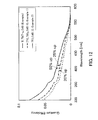
- the photoelectrochemical cell 100 of the present example thus produced was measured for quantum efficiency with respect to light having a wavelength of 300 nm to 600 nm.
- FIG. 12 shows the result thereof.
- the method of measuring the quantum efficiency was as follows.
- Quantum efficiency (Value of current generated in irradiation at each wavelength) / (Number of photons at each wavelength)
- a sodium sulfite aqueous solution containing sodium sulfide was used as the electrolyte in the photoelectrochemical cell of present example.
- the reaction that proceeded in the semiconductor electrode was not an oxygen evolution reaction according to the above-mentioned reaction formula (1) but a reaction according to the above-mentioned reaction formula (3).
- the reaction expressed by the aforementioned reaction formula (2) proceeded in the counter electrode.
- Comparative Example 1 a photoelectrochemical cell in which only the configuration of the semiconductor electrode was different from that in Example was produced.
- a 150 nm-thick titanium oxide film (anatase polycrystalline material) was formed on a 10 mm x 50 mm ITO substrate (with a thickness of 150 nm) by sputtering, and a 500 nm-thick cadmium sulfide film further was formed thereon in the same manner as in Example.
- the semiconductor electrode of Comparative Example 1 was produced in which the titanium oxide film was disposed, as the first n-type semiconductor layer, on the conductor composed of ITO, and the cadmium sulfide film further was disposed thereon as the second n-type semiconductor layer. That is, in Comparative Example 1, the semiconductor electrode had a configuration in which the first n-type semiconductor layer did not have the nanotube array structure.
- the photoelectrochemical cell of Comparative Example 1 thus produced was measured for quantum efficiency with respect to light having a wavelength of 300 nm to 600 nm, by the same method as in Example.
- FIG. 12 shows the result thereof.
- Comparative Example 2 a photoelectrochemical cell in which only the configuration of the semiconductor electrode was different from that in Example was produced.
- a 500 nm-thick cadmium sulfide film was formed on a 10 mm x 50 mm ITO substrate (with a thickness of 150 nm) by chemical deposition.
- the semiconductor electrode was produced in which the cadmium sulfide film was disposed directly on the conductor composed of ITO. That is, the semiconductor electrode of Comparative Example 2 had a configuration in which the first n-type semiconductor layer having the nanotube array structure was omitted and only the second n-type semiconductor layer was disposed on the conductor.
- the photoelectrochemical cell of Comparative Example 2 thus produced was measured for quantum efficiency with respect to light having a wavelength of 300 nm to 600 nm, by the same method as in Example.
- FIG. 12 shows the result thereof.
- the quantum efficiency started increasing at around 550 nm that is the absorption edge of cadmium sulfide. Throughout the wavelength range of 550 nm or less, the quantum efficiency was enhanced by about 50% from that in the case (Comparative Example 2) where the first n-type semiconductor layer was omitted, and by about 25% from that in the case (Comparative Example 1) where not the titanium oxide nanotubes but the smooth titanium oxide film was used for the first n-type semiconductor layer. Comparing Comparative Example 1 with Comparative Example 2, the quantum efficiency in Comparative Example 1 using the titanium oxide film was enhanced by about 20% from the quantum efficiency in Comparative Example 2.
- the quantum efficiency was enhanced in Example because in the semiconductor electrode of Example, the titanium oxide nanotubes were used as the first n-type semiconductor layer and thereby the first n-type semiconductor layer had a large surface area as well as high crystallinity.
- the titanium oxide nanotube array was used in Example as the first n-type semiconductor layer having the nanotube structure, the material of the nanotube array is not limited to titanium oxide.
- cadmium sulfide was used for the second n-type semiconductor layer, the material of the second n-type semiconductor layer is not limited to cadmium sulfide, and a semiconductor, such as TaON and Ta 3 N 5 , also may be used.
- the photoelectrochemical cell and the energy system according to the present invention can improve the quantum efficiency of the hydrogen evolution reaction by irradiation with light, and thus are useful as a domestic power generation system and the like.
Landscapes
- Chemical & Material Sciences (AREA)
- Chemical Kinetics & Catalysis (AREA)
- Engineering & Computer Science (AREA)
- Electrochemistry (AREA)
- Organic Chemistry (AREA)
- General Chemical & Material Sciences (AREA)
- Inorganic Chemistry (AREA)
- Combustion & Propulsion (AREA)
- Health & Medical Sciences (AREA)
- General Health & Medical Sciences (AREA)
- Life Sciences & Earth Sciences (AREA)
- Manufacturing & Machinery (AREA)
- Sustainable Development (AREA)
- Sustainable Energy (AREA)
- Materials Engineering (AREA)
- Metallurgy (AREA)
- Electrolytic Production Of Non-Metals, Compounds, Apparatuses Therefor (AREA)
- Electrodes For Compound Or Non-Metal Manufacture (AREA)
- Hybrid Cells (AREA)
Applications Claiming Priority (2)
| Application Number | Priority Date | Filing Date | Title |
|---|---|---|---|
| JP2009257437 | 2009-11-10 | ||
| PCT/JP2010/006498 WO2011058723A1 (ja) | 2009-11-10 | 2010-11-04 | 光電気化学セル及びそれを用いたエネルギーシステム |
Publications (3)
| Publication Number | Publication Date |
|---|---|
| EP2500449A1 true EP2500449A1 (de) | 2012-09-19 |
| EP2500449A4 EP2500449A4 (de) | 2014-04-09 |
| EP2500449B1 EP2500449B1 (de) | 2017-09-27 |
Family
ID=43991393
Family Applications (1)
| Application Number | Title | Priority Date | Filing Date |
|---|---|---|---|
| EP10829688.0A Not-in-force EP2500449B1 (de) | 2009-11-10 | 2010-11-04 | Photoelektrochemische zelle und diese enthaltendes energiesystem |
Country Status (5)
| Country | Link |
|---|---|
| US (1) | US8821700B2 (de) |
| EP (1) | EP2500449B1 (de) |
| JP (1) | JP4791614B2 (de) |
| CN (1) | CN102575361B (de) |
| WO (1) | WO2011058723A1 (de) |
Families Citing this family (20)
| Publication number | Priority date | Publication date | Assignee | Title |
|---|---|---|---|---|
| US9057144B2 (en) * | 2010-07-30 | 2015-06-16 | University Of Utah Research Foundation | Nanostructured films and related methods |
| JP5565728B2 (ja) * | 2010-08-10 | 2014-08-06 | 学校法人同志社 | チタニアナノチューブアレイおよびチタニア電極の作成方法、チタニア電極、並びにこのチタニア電極を適用した色素増感太陽電池 |
| CN103403940B (zh) * | 2011-03-08 | 2016-03-16 | 松下知识产权经营株式会社 | 能量系统 |
| JP5664379B2 (ja) * | 2011-03-18 | 2015-02-04 | 国立大学法人 新潟大学 | 水の可視光分解用アノード電極及び水の可視光分解装置 |
| US9755023B2 (en) * | 2011-09-30 | 2017-09-05 | The University Of Kentucky Research Foundation | Photoelectrochemical cell including Ga(Sbx)N1-x semiconductor electrode |
| JP5837405B2 (ja) * | 2011-11-28 | 2015-12-24 | 独立行政法人国立高等専門学校機構 | 光電変換素子及びその製造方法 |
| CN104662204B (zh) * | 2012-10-31 | 2017-05-03 | 松下知识产权经营株式会社 | 光半导体电极、光电化学电池以及能量系统 |
| JP6201155B2 (ja) * | 2013-02-21 | 2017-09-27 | パナソニックIpマネジメント株式会社 | 水素生成デバイスおよび水素生成ユニットならびにそれらを用いたエネルギーシステム |
| AU2014258911A1 (en) * | 2013-04-26 | 2015-01-15 | Panasonic Corporation | Optical semiconductor electrode, and water photolysis method using photoelectrochemical cell provided with same |
| AU2014258898B2 (en) * | 2013-04-26 | 2016-04-28 | Panasonic Intellectual Property Management Co., Ltd. | Method for generating hydrogen, and hydrogen generating device used in said method |
| CN103757656B (zh) * | 2014-01-20 | 2016-02-03 | 中国工程物理研究院化工材料研究所 | 结合原电池和光电化学电池的光电化学制氢装置 |
| JP6271311B2 (ja) * | 2014-03-24 | 2018-01-31 | 株式会社東芝 | 電気化学反応装置 |
| US9776162B2 (en) * | 2014-08-14 | 2017-10-03 | Council Of Scientific & Industrial Research | CuO—TiO2 nanocomposite photocatalyst for hydrogen production, process for the preparation thereof |
| CN104638276A (zh) * | 2014-12-03 | 2015-05-20 | 南京大学 | 一种光电化学池及其制备方法 |
| FR3046425B1 (fr) * | 2016-01-04 | 2018-01-12 | Commissariat A L'energie Atomique Et Aux Energies Alternatives | Photocathode pour un dispositif de photoelectrolyse, un procede de fabrication d'une telle photocathode et un dispositif de photoelectrolyse |
| CN106435636B (zh) * | 2016-10-26 | 2018-07-03 | 中盈长江国际新能源投资有限公司 | 光补电电解水制氢微电极光纤、光缆及制氢装置 |
| JP6715172B2 (ja) * | 2016-12-05 | 2020-07-01 | 日本電信電話株式会社 | 半導体光電極の製造方法 |
| JP6649237B2 (ja) * | 2016-12-06 | 2020-02-19 | 日本電信電話株式会社 | 光触媒酸化還元反応装置 |
| KR102155363B1 (ko) | 2018-10-31 | 2020-09-11 | 한국생산기술연구원 | 광전기화학전지용 광전극 및 그 제조방법과 광전극을 포함하는 광전기화학전지 |
| JP2023044105A (ja) * | 2021-09-17 | 2023-03-30 | 株式会社日立製作所 | アノード光電極、アノード光電極の製造方法および水素製造設備 |
Citations (5)
| Publication number | Priority date | Publication date | Assignee | Title |
|---|---|---|---|---|
| US4090933A (en) * | 1975-11-17 | 1978-05-23 | Allied Chemical Corporation | Photoelectrolysis of water by solar radiation |
| US4461691A (en) * | 1983-02-10 | 1984-07-24 | The United States Of America As Represented By The United States Department Of Energy | Organic conductive films for semiconductor electrodes |
| US4466869A (en) * | 1983-08-15 | 1984-08-21 | Energy Conversion Devices, Inc. | Photolytic production of hydrogen |
| JP2006302695A (ja) * | 2005-04-21 | 2006-11-02 | Nissan Motor Co Ltd | 光電気化学セル及びその製造方法 |
| WO2008060293A2 (en) * | 2005-12-13 | 2008-05-22 | University Of Nevada, Reno | Preparation of nano-tubular titania substrates having gold and carbon particles deposited thereon and their use in photo-electrolysis of water |
Family Cites Families (20)
| Publication number | Priority date | Publication date | Assignee | Title |
|---|---|---|---|---|
| JPS51123779A (en) | 1975-04-23 | 1976-10-28 | Kenichi Honda | A hydrogen-oxygen drawing method using electrochemical photoelectric c ells |
| US4061555A (en) * | 1977-01-19 | 1977-12-06 | Rca Corporation | Water photolysis apparatus |
| US4181754A (en) * | 1978-06-22 | 1980-01-01 | Gte Laboratories Incorporated | In situ method of preparing modified titanium dioxide photoactive electrodes |
| US4203814A (en) * | 1978-11-01 | 1980-05-20 | United Technologies Corporation | Hydrogen gas generation utilizing a bromide electrolyte and radiant energy |
| US4251289A (en) * | 1979-12-28 | 1981-02-17 | Exxon Research & Engineering Co. | Gradient doping in amorphous silicon |
| US4310405A (en) * | 1980-09-23 | 1982-01-12 | Bell Telephone Laboratories, Incorporated | Device for the photoelectrochemical generation of hydrogen at p-type semiconductor electrodes |
| JP2002234105A (ja) | 2000-03-13 | 2002-08-20 | Toto Ltd | 親水性部材及びその製造方法 |
| JP4590579B2 (ja) | 2000-11-07 | 2010-12-01 | 独立行政法人 日本原子力研究開発機構 | 高効率光触媒薄膜及びその製造方法 |
| US6605832B2 (en) * | 2001-07-31 | 2003-08-12 | Xerox Corporation | Semiconductor structures having reduced contact resistance |
| JP3666588B2 (ja) | 2001-11-21 | 2005-06-29 | 独立行政法人科学技術振興機構 | 多層薄膜状光触媒を用いた水素の製造方法 |
| US7485799B2 (en) * | 2002-05-07 | 2009-02-03 | John Michael Guerra | Stress-induced bandgap-shifted semiconductor photoelectrolytic/photocatalytic/photovoltaic surface and method for making same |
| CN1485003A (zh) | 2002-09-24 | 2004-03-31 | 中国科学技术大学 | 利用液化天然气冷能半导体温差发电及制氢的方法与装置 |
| US7052587B2 (en) * | 2003-06-27 | 2006-05-30 | General Motors Corporation | Photoelectrochemical device and electrode |
| WO2005101510A2 (en) * | 2004-04-16 | 2005-10-27 | The University Of Toledo | Light-assisted electrochemical shunt passivation for photovoltaic devices |
| CA2621995A1 (en) | 2005-09-09 | 2007-10-25 | University Of Nevada, Reno | Preparation of nano-tubular titania substrate with oxygen vacancies and their use in photo-electrolysis of water |
| JP2007214117A (ja) * | 2006-01-12 | 2007-08-23 | Matsushita Electric Ind Co Ltd | 電子放出装置及びこれを用いた電磁波発生装置 |
| US7808169B2 (en) | 2006-01-12 | 2010-10-05 | Panasonic Corporation | Electron emitting device and electromagnetic wave generating device using the same |
| US7481914B2 (en) * | 2006-03-31 | 2009-01-27 | General Electric Company | Photoelectrolysis cells, and related devices and processes |
| JP2008104899A (ja) | 2006-10-23 | 2008-05-08 | Sharp Corp | 光触媒膜、光触媒膜の製造方法およびこれを用いた水素発生装置 |
| EP2351873B1 (de) * | 2008-10-30 | 2018-03-21 | Panasonic Intellectual Property Management Co., Ltd. | Photoelektrochemische zelle und diese enthaltendes energiesystem |
-
2010
- 2010-11-04 WO PCT/JP2010/006498 patent/WO2011058723A1/ja active Application Filing
- 2010-11-04 JP JP2011517686A patent/JP4791614B2/ja not_active Expired - Fee Related
- 2010-11-04 US US13/502,322 patent/US8821700B2/en not_active Expired - Fee Related
- 2010-11-04 CN CN201080046454.2A patent/CN102575361B/zh not_active Expired - Fee Related
- 2010-11-04 EP EP10829688.0A patent/EP2500449B1/de not_active Not-in-force
Patent Citations (5)
| Publication number | Priority date | Publication date | Assignee | Title |
|---|---|---|---|---|
| US4090933A (en) * | 1975-11-17 | 1978-05-23 | Allied Chemical Corporation | Photoelectrolysis of water by solar radiation |
| US4461691A (en) * | 1983-02-10 | 1984-07-24 | The United States Of America As Represented By The United States Department Of Energy | Organic conductive films for semiconductor electrodes |
| US4466869A (en) * | 1983-08-15 | 1984-08-21 | Energy Conversion Devices, Inc. | Photolytic production of hydrogen |
| JP2006302695A (ja) * | 2005-04-21 | 2006-11-02 | Nissan Motor Co Ltd | 光電気化学セル及びその製造方法 |
| WO2008060293A2 (en) * | 2005-12-13 | 2008-05-22 | University Of Nevada, Reno | Preparation of nano-tubular titania substrates having gold and carbon particles deposited thereon and their use in photo-electrolysis of water |
Non-Patent Citations (1)
| Title |
|---|
| See also references of WO2011058723A1 * |
Also Published As
| Publication number | Publication date |
|---|---|
| WO2011058723A1 (ja) | 2011-05-19 |
| US8821700B2 (en) | 2014-09-02 |
| JP4791614B2 (ja) | 2011-10-12 |
| CN102575361A (zh) | 2012-07-11 |
| CN102575361B (zh) | 2014-08-20 |
| US20120276464A1 (en) | 2012-11-01 |
| JPWO2011058723A1 (ja) | 2013-03-28 |
| EP2500449B1 (de) | 2017-09-27 |
| EP2500449A4 (de) | 2014-04-09 |
Similar Documents
| Publication | Publication Date | Title |
|---|---|---|
| EP2500449B1 (de) | Photoelektrochemische zelle und diese enthaltendes energiesystem | |
| EP2351873B1 (de) | Photoelektrochemische zelle und diese enthaltendes energiesystem | |
| EP2555314B1 (de) | Photoelektrochemische zelle und energiesystem damit | |
| US8758578B2 (en) | Photoelectrochemical cell and energy system using the same | |
| KR102014990B1 (ko) | 광전극 구조체용 복합 보호층, 이를 포함하는 광전극 구조체 및 이를 포함하는 광전기화학 전지 | |
| US20160333485A1 (en) | Method for producing photoelectrode | |
| AU2016374872B2 (en) | Substrate-electrode (SE) interface illuminated photoelectrodes and photoelectrochemical cells | |
| US20200385873A1 (en) | Photocatalytic electrode for water splitting and water splitting device | |
| EP2915907B1 (de) | Lichthalbleiterelektrode, fotoelektrochemische zelle und energiesystem | |
| EP2817437B1 (de) | Photovoltaische hybrid-elektrolysezelle | |
| US20150111118A1 (en) | Photoelectrochemical cell and hydrogen generation method using the same | |
| US20060100100A1 (en) | Tetrahedrally-bonded oxide semiconductors for photoelectrochemical hydrogen production | |
| JP2008214122A (ja) | 半導体酸化物膜およびその製造方法、ならびに半導体酸化物膜を用いた水素発生装置 | |
| JP2012114016A (ja) | 光電気化学電池及びそれを用いたエネルギーシステム |
Legal Events
| Date | Code | Title | Description |
|---|---|---|---|
| PUAI | Public reference made under article 153(3) epc to a published international application that has entered the european phase |
Free format text: ORIGINAL CODE: 0009012 |
|
| 17P | Request for examination filed |
Effective date: 20120611 |
|
| AK | Designated contracting states |
Kind code of ref document: A1 Designated state(s): AL AT BE BG CH CY CZ DE DK EE ES FI FR GB GR HR HU IE IS IT LI LT LU LV MC MK MT NL NO PL PT RO RS SE SI SK SM TR |
|
| DAX | Request for extension of the european patent (deleted) | ||
| A4 | Supplementary search report drawn up and despatched |
Effective date: 20140307 |
|
| RIC1 | Information provided on ipc code assigned before grant |
Ipc: C25B 1/00 20060101ALI20140304BHEP Ipc: C01B 3/04 20060101AFI20140304BHEP Ipc: H01M 14/00 20060101ALI20140304BHEP |
|
| RAP1 | Party data changed (applicant data changed or rights of an application transferred) |
Owner name: PANASONIC INTELLECTUAL PROPERTY MANAGEMENT CO., LT |
|
| REG | Reference to a national code |
Ref country code: DE Ref legal event code: R079 Ref document number: 602010045627 Country of ref document: DE Free format text: PREVIOUS MAIN CLASS: C25B0009000000 Ipc: C25B0001000000 |
|
| RIC1 | Information provided on ipc code assigned before grant |
Ipc: C25B 1/00 20060101AFI20170412BHEP |
|
| GRAP | Despatch of communication of intention to grant a patent |
Free format text: ORIGINAL CODE: EPIDOSNIGR1 |
|
| STAA | Information on the status of an ep patent application or granted ep patent |
Free format text: STATUS: GRANT OF PATENT IS INTENDED |
|
| INTG | Intention to grant announced |
Effective date: 20170524 |
|
| GRAS | Grant fee paid |
Free format text: ORIGINAL CODE: EPIDOSNIGR3 |
|
| GRAA | (expected) grant |
Free format text: ORIGINAL CODE: 0009210 |
|
| STAA | Information on the status of an ep patent application or granted ep patent |
Free format text: STATUS: THE PATENT HAS BEEN GRANTED |
|
| AK | Designated contracting states |
Kind code of ref document: B1 Designated state(s): AL AT BE BG CH CY CZ DE DK EE ES FI FR GB GR HR HU IE IS IT LI LT LU LV MC MK MT NL NO PL PT RO RS SE SI SK SM TR |
|
| REG | Reference to a national code |
Ref country code: GB Ref legal event code: FG4D |
|
| REG | Reference to a national code |
Ref country code: CH Ref legal event code: EP |
|
| REG | Reference to a national code |
Ref country code: AT Ref legal event code: REF Ref document number: 932049 Country of ref document: AT Kind code of ref document: T Effective date: 20171015 |
|
| REG | Reference to a national code |
Ref country code: IE Ref legal event code: FG4D |
|
| REG | Reference to a national code |
Ref country code: DE Ref legal event code: R096 Ref document number: 602010045627 Country of ref document: DE |
|
| PG25 | Lapsed in a contracting state [announced via postgrant information from national office to epo] |
Ref country code: FI Free format text: LAPSE BECAUSE OF FAILURE TO SUBMIT A TRANSLATION OF THE DESCRIPTION OR TO PAY THE FEE WITHIN THE PRESCRIBED TIME-LIMIT Effective date: 20170927 Ref country code: NO Free format text: LAPSE BECAUSE OF FAILURE TO SUBMIT A TRANSLATION OF THE DESCRIPTION OR TO PAY THE FEE WITHIN THE PRESCRIBED TIME-LIMIT Effective date: 20171227 Ref country code: SE Free format text: LAPSE BECAUSE OF FAILURE TO SUBMIT A TRANSLATION OF THE DESCRIPTION OR TO PAY THE FEE WITHIN THE PRESCRIBED TIME-LIMIT Effective date: 20170927 Ref country code: LT Free format text: LAPSE BECAUSE OF FAILURE TO SUBMIT A TRANSLATION OF THE DESCRIPTION OR TO PAY THE FEE WITHIN THE PRESCRIBED TIME-LIMIT Effective date: 20170927 Ref country code: HR Free format text: LAPSE BECAUSE OF FAILURE TO SUBMIT A TRANSLATION OF THE DESCRIPTION OR TO PAY THE FEE WITHIN THE PRESCRIBED TIME-LIMIT Effective date: 20170927 |
|
| REG | Reference to a national code |
Ref country code: NL Ref legal event code: MP Effective date: 20170927 |
|
| REG | Reference to a national code |
Ref country code: LT Ref legal event code: MG4D |
|
| REG | Reference to a national code |
Ref country code: AT Ref legal event code: MK05 Ref document number: 932049 Country of ref document: AT Kind code of ref document: T Effective date: 20170927 |
|
| PG25 | Lapsed in a contracting state [announced via postgrant information from national office to epo] |
Ref country code: RS Free format text: LAPSE BECAUSE OF FAILURE TO SUBMIT A TRANSLATION OF THE DESCRIPTION OR TO PAY THE FEE WITHIN THE PRESCRIBED TIME-LIMIT Effective date: 20170927 Ref country code: LV Free format text: LAPSE BECAUSE OF FAILURE TO SUBMIT A TRANSLATION OF THE DESCRIPTION OR TO PAY THE FEE WITHIN THE PRESCRIBED TIME-LIMIT Effective date: 20170927 Ref country code: BG Free format text: LAPSE BECAUSE OF FAILURE TO SUBMIT A TRANSLATION OF THE DESCRIPTION OR TO PAY THE FEE WITHIN THE PRESCRIBED TIME-LIMIT Effective date: 20171227 Ref country code: GR Free format text: LAPSE BECAUSE OF FAILURE TO SUBMIT A TRANSLATION OF THE DESCRIPTION OR TO PAY THE FEE WITHIN THE PRESCRIBED TIME-LIMIT Effective date: 20171228 |
|
| PG25 | Lapsed in a contracting state [announced via postgrant information from national office to epo] |
Ref country code: NL Free format text: LAPSE BECAUSE OF FAILURE TO SUBMIT A TRANSLATION OF THE DESCRIPTION OR TO PAY THE FEE WITHIN THE PRESCRIBED TIME-LIMIT Effective date: 20170927 |
|
| PG25 | Lapsed in a contracting state [announced via postgrant information from national office to epo] |
Ref country code: ES Free format text: LAPSE BECAUSE OF FAILURE TO SUBMIT A TRANSLATION OF THE DESCRIPTION OR TO PAY THE FEE WITHIN THE PRESCRIBED TIME-LIMIT Effective date: 20170927 Ref country code: RO Free format text: LAPSE BECAUSE OF FAILURE TO SUBMIT A TRANSLATION OF THE DESCRIPTION OR TO PAY THE FEE WITHIN THE PRESCRIBED TIME-LIMIT Effective date: 20170927 Ref country code: CZ Free format text: LAPSE BECAUSE OF FAILURE TO SUBMIT A TRANSLATION OF THE DESCRIPTION OR TO PAY THE FEE WITHIN THE PRESCRIBED TIME-LIMIT Effective date: 20170927 |
|
| PG25 | Lapsed in a contracting state [announced via postgrant information from national office to epo] |
Ref country code: AT Free format text: LAPSE BECAUSE OF FAILURE TO SUBMIT A TRANSLATION OF THE DESCRIPTION OR TO PAY THE FEE WITHIN THE PRESCRIBED TIME-LIMIT Effective date: 20170927 Ref country code: EE Free format text: LAPSE BECAUSE OF FAILURE TO SUBMIT A TRANSLATION OF THE DESCRIPTION OR TO PAY THE FEE WITHIN THE PRESCRIBED TIME-LIMIT Effective date: 20170927 Ref country code: IS Free format text: LAPSE BECAUSE OF FAILURE TO SUBMIT A TRANSLATION OF THE DESCRIPTION OR TO PAY THE FEE WITHIN THE PRESCRIBED TIME-LIMIT Effective date: 20180127 Ref country code: SM Free format text: LAPSE BECAUSE OF FAILURE TO SUBMIT A TRANSLATION OF THE DESCRIPTION OR TO PAY THE FEE WITHIN THE PRESCRIBED TIME-LIMIT Effective date: 20170927 Ref country code: SK Free format text: LAPSE BECAUSE OF FAILURE TO SUBMIT A TRANSLATION OF THE DESCRIPTION OR TO PAY THE FEE WITHIN THE PRESCRIBED TIME-LIMIT Effective date: 20170927 Ref country code: IT Free format text: LAPSE BECAUSE OF FAILURE TO SUBMIT A TRANSLATION OF THE DESCRIPTION OR TO PAY THE FEE WITHIN THE PRESCRIBED TIME-LIMIT Effective date: 20170927 |
|
| REG | Reference to a national code |
Ref country code: DE Ref legal event code: R097 Ref document number: 602010045627 Country of ref document: DE |
|
| PG25 | Lapsed in a contracting state [announced via postgrant information from national office to epo] |
Ref country code: MC Free format text: LAPSE BECAUSE OF FAILURE TO SUBMIT A TRANSLATION OF THE DESCRIPTION OR TO PAY THE FEE WITHIN THE PRESCRIBED TIME-LIMIT Effective date: 20170927 |
|
| PG25 | Lapsed in a contracting state [announced via postgrant information from national office to epo] |
Ref country code: LI Free format text: LAPSE BECAUSE OF NON-PAYMENT OF DUE FEES Effective date: 20171130 Ref country code: DK Free format text: LAPSE BECAUSE OF FAILURE TO SUBMIT A TRANSLATION OF THE DESCRIPTION OR TO PAY THE FEE WITHIN THE PRESCRIBED TIME-LIMIT Effective date: 20170927 Ref country code: CH Free format text: LAPSE BECAUSE OF NON-PAYMENT OF DUE FEES Effective date: 20171130 |
|
| PLBE | No opposition filed within time limit |
Free format text: ORIGINAL CODE: 0009261 |
|
| STAA | Information on the status of an ep patent application or granted ep patent |
Free format text: STATUS: NO OPPOSITION FILED WITHIN TIME LIMIT |
|
| GBPC | Gb: european patent ceased through non-payment of renewal fee |
Effective date: 20171227 |
|
| PG25 | Lapsed in a contracting state [announced via postgrant information from national office to epo] |
Ref country code: LU Free format text: LAPSE BECAUSE OF NON-PAYMENT OF DUE FEES Effective date: 20171104 Ref country code: PL Free format text: LAPSE BECAUSE OF FAILURE TO SUBMIT A TRANSLATION OF THE DESCRIPTION OR TO PAY THE FEE WITHIN THE PRESCRIBED TIME-LIMIT Effective date: 20170927 |
|
| REG | Reference to a national code |
Ref country code: FR Ref legal event code: ST Effective date: 20180731 Ref country code: BE Ref legal event code: MM Effective date: 20171130 |
|
| 26N | No opposition filed |
Effective date: 20180628 |
|
| REG | Reference to a national code |
Ref country code: IE Ref legal event code: MM4A |
|
| PG25 | Lapsed in a contracting state [announced via postgrant information from national office to epo] |
Ref country code: MT Free format text: LAPSE BECAUSE OF NON-PAYMENT OF DUE FEES Effective date: 20171104 |
|
| PG25 | Lapsed in a contracting state [announced via postgrant information from national office to epo] |
Ref country code: IE Free format text: LAPSE BECAUSE OF NON-PAYMENT OF DUE FEES Effective date: 20171104 Ref country code: FR Free format text: LAPSE BECAUSE OF NON-PAYMENT OF DUE FEES Effective date: 20171130 |
|
| PG25 | Lapsed in a contracting state [announced via postgrant information from national office to epo] |
Ref country code: SI Free format text: LAPSE BECAUSE OF FAILURE TO SUBMIT A TRANSLATION OF THE DESCRIPTION OR TO PAY THE FEE WITHIN THE PRESCRIBED TIME-LIMIT Effective date: 20170927 Ref country code: BE Free format text: LAPSE BECAUSE OF NON-PAYMENT OF DUE FEES Effective date: 20171130 Ref country code: GB Free format text: LAPSE BECAUSE OF NON-PAYMENT OF DUE FEES Effective date: 20171227 |
|
| PGFP | Annual fee paid to national office [announced via postgrant information from national office to epo] |
Ref country code: DE Payment date: 20181120 Year of fee payment: 9 |
|
| PG25 | Lapsed in a contracting state [announced via postgrant information from national office to epo] |
Ref country code: HU Free format text: LAPSE BECAUSE OF FAILURE TO SUBMIT A TRANSLATION OF THE DESCRIPTION OR TO PAY THE FEE WITHIN THE PRESCRIBED TIME-LIMIT; INVALID AB INITIO Effective date: 20101104 |
|
| PG25 | Lapsed in a contracting state [announced via postgrant information from national office to epo] |
Ref country code: CY Free format text: LAPSE BECAUSE OF NON-PAYMENT OF DUE FEES Effective date: 20170927 |
|
| PG25 | Lapsed in a contracting state [announced via postgrant information from national office to epo] |
Ref country code: MK Free format text: LAPSE BECAUSE OF FAILURE TO SUBMIT A TRANSLATION OF THE DESCRIPTION OR TO PAY THE FEE WITHIN THE PRESCRIBED TIME-LIMIT Effective date: 20170927 |
|
| PG25 | Lapsed in a contracting state [announced via postgrant information from national office to epo] |
Ref country code: TR Free format text: LAPSE BECAUSE OF FAILURE TO SUBMIT A TRANSLATION OF THE DESCRIPTION OR TO PAY THE FEE WITHIN THE PRESCRIBED TIME-LIMIT Effective date: 20170927 |
|
| PG25 | Lapsed in a contracting state [announced via postgrant information from national office to epo] |
Ref country code: PT Free format text: LAPSE BECAUSE OF FAILURE TO SUBMIT A TRANSLATION OF THE DESCRIPTION OR TO PAY THE FEE WITHIN THE PRESCRIBED TIME-LIMIT Effective date: 20170927 |
|
| REG | Reference to a national code |
Ref country code: DE Ref legal event code: R119 Ref document number: 602010045627 Country of ref document: DE |
|
| PG25 | Lapsed in a contracting state [announced via postgrant information from national office to epo] |
Ref country code: AL Free format text: LAPSE BECAUSE OF FAILURE TO SUBMIT A TRANSLATION OF THE DESCRIPTION OR TO PAY THE FEE WITHIN THE PRESCRIBED TIME-LIMIT Effective date: 20170927 |
|
| PG25 | Lapsed in a contracting state [announced via postgrant information from national office to epo] |
Ref country code: DE Free format text: LAPSE BECAUSE OF NON-PAYMENT OF DUE FEES Effective date: 20200603 |