EP2498306B1 - Lichtemittierende Diode mit großem Betrachtungswinkel und Herstellungsverfahren dafür - Google Patents
Lichtemittierende Diode mit großem Betrachtungswinkel und Herstellungsverfahren dafür Download PDFInfo
- Publication number
- EP2498306B1 EP2498306B1 EP12158431.2A EP12158431A EP2498306B1 EP 2498306 B1 EP2498306 B1 EP 2498306B1 EP 12158431 A EP12158431 A EP 12158431A EP 2498306 B1 EP2498306 B1 EP 2498306B1
- Authority
- EP
- European Patent Office
- Prior art keywords
- layer
- type semiconductor
- light emitting
- emitting diode
- transparent conductive
- Prior art date
- Legal status (The legal status is an assumption and is not a legal conclusion. Google has not performed a legal analysis and makes no representation as to the accuracy of the status listed.)
- Active
Links
Images


Classifications
-
- H—ELECTRICITY
- H10—SEMICONDUCTOR DEVICES; ELECTRIC SOLID-STATE DEVICES NOT OTHERWISE PROVIDED FOR
- H10H—INORGANIC LIGHT-EMITTING SEMICONDUCTOR DEVICES HAVING POTENTIAL BARRIERS
- H10H20/00—Individual inorganic light-emitting semiconductor devices having potential barriers, e.g. light-emitting diodes [LED]
- H10H20/80—Constructional details
- H10H20/81—Bodies
- H10H20/819—Bodies characterised by their shape, e.g. curved or truncated substrates
- H10H20/82—Roughened surfaces, e.g. at the interface between epitaxial layers
-
- H—ELECTRICITY
- H10—SEMICONDUCTOR DEVICES; ELECTRIC SOLID-STATE DEVICES NOT OTHERWISE PROVIDED FOR
- H10H—INORGANIC LIGHT-EMITTING SEMICONDUCTOR DEVICES HAVING POTENTIAL BARRIERS
- H10H20/00—Individual inorganic light-emitting semiconductor devices having potential barriers, e.g. light-emitting diodes [LED]
- H10H20/80—Constructional details
- H10H20/81—Bodies
- H10H20/819—Bodies characterised by their shape, e.g. curved or truncated substrates
-
- H—ELECTRICITY
- H10—SEMICONDUCTOR DEVICES; ELECTRIC SOLID-STATE DEVICES NOT OTHERWISE PROVIDED FOR
- H10H—INORGANIC LIGHT-EMITTING SEMICONDUCTOR DEVICES HAVING POTENTIAL BARRIERS
- H10H20/00—Individual inorganic light-emitting semiconductor devices having potential barriers, e.g. light-emitting diodes [LED]
- H10H20/01—Manufacture or treatment
- H10H20/011—Manufacture or treatment of bodies, e.g. forming semiconductor layers
- H10H20/013—Manufacture or treatment of bodies, e.g. forming semiconductor layers having light-emitting regions comprising only Group III-V materials
-
- H—ELECTRICITY
- H10—SEMICONDUCTOR DEVICES; ELECTRIC SOLID-STATE DEVICES NOT OTHERWISE PROVIDED FOR
- H10H—INORGANIC LIGHT-EMITTING SEMICONDUCTOR DEVICES HAVING POTENTIAL BARRIERS
- H10H20/00—Individual inorganic light-emitting semiconductor devices having potential barriers, e.g. light-emitting diodes [LED]
- H10H20/80—Constructional details
- H10H20/81—Bodies
- H10H20/813—Bodies having a plurality of light-emitting regions, e.g. multi-junction LEDs or light-emitting devices having photoluminescent regions within the bodies
-
- H—ELECTRICITY
- H10—SEMICONDUCTOR DEVICES; ELECTRIC SOLID-STATE DEVICES NOT OTHERWISE PROVIDED FOR
- H10H—INORGANIC LIGHT-EMITTING SEMICONDUCTOR DEVICES HAVING POTENTIAL BARRIERS
- H10H20/00—Individual inorganic light-emitting semiconductor devices having potential barriers, e.g. light-emitting diodes [LED]
- H10H20/80—Constructional details
- H10H20/83—Electrodes
-
- H—ELECTRICITY
- H10—SEMICONDUCTOR DEVICES; ELECTRIC SOLID-STATE DEVICES NOT OTHERWISE PROVIDED FOR
- H10H—INORGANIC LIGHT-EMITTING SEMICONDUCTOR DEVICES HAVING POTENTIAL BARRIERS
- H10H20/00—Individual inorganic light-emitting semiconductor devices having potential barriers, e.g. light-emitting diodes [LED]
- H10H20/80—Constructional details
- H10H20/81—Bodies
-
- H—ELECTRICITY
- H10—SEMICONDUCTOR DEVICES; ELECTRIC SOLID-STATE DEVICES NOT OTHERWISE PROVIDED FOR
- H10W—GENERIC PACKAGES, INTERCONNECTIONS, CONNECTORS OR OTHER CONSTRUCTIONAL DETAILS OF DEVICES COVERED BY CLASS H10
- H10W72/00—Interconnections or connectors in packages
- H10W72/50—Bond wires
- H10W72/551—Materials of bond wires
- H10W72/552—Materials of bond wires comprising metals or metalloids, e.g. silver
Definitions
- Taiwan Patent Application No. 100107808 filed March 8, 2011
- Taiwan Patent Application No. 100138543 filed October 24, 2011 .
- the present invention relates to a light emitting diode, and more particularly to a light emitting diode with a large viewing angle.
- the present invention relates to a method of fabricating such a light emitting diode.
- gallium nitride-type light emitting diodes e.g. GaN, AIGaN, InGaN or AllnGaN light emitting diodes
- the refractive index difference at the interface between the semiconductor and the air may result in a total reflection phenomenon. Due to the total reflection phenomenon, the viewing angle of the light emitting diode is restricted. Consequently, the researchers make efforts in developing a method for increasing the viewing angle of the light emitting diode.
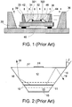
- FIG. 1 schematically illustrates a conventional light emitting diode package disclosed in US Patent Publication No. 20090085053 .
- the light emitting diode package comprises a substrate 30, a LED chip 32, a transparent housing body 33, a phosphor matrix 34, and an outer reflector 36.
- the substrate 30 has an upper surface 38 and a lower surface 40.
- a first electrode 42 and a second electrode 44 are disposed on the substrate 30.
- the LED chip 32 is mounted on the upper surface 38 of the substrate 30.
- the LED chip 32 has a positive electrode 321 and a negative electrode 322.
- the positive electrode 321 of the LED chip 32 is connected with the first electrode 42 of the substrate 30 through a wire 46, and the negative electrode 322 of the LED chip 32 is connected with the second electrode 44 of the substrate 30 by the wire 46.
- the transparent housing body 33 is disposed on the upper surface 38 of the substrate 30, and has a cavity 39.
- the LED chip 32 is disposed within the cavity 39.
- the phosphor matrix 34 is inserted in the cavity 39. Consequently, the light emitted by the LED chip 32 may be transmitted through the phosphor matrix 34 and converted into white light.
- the white light may be transmitted through the lateral sides of the transparent housing body 33.
- the light transmitted through the lateral sides of the transparent housing body 33 is reflected by the outer reflector 36, so that the intensity of the light from the LED chip 32 is enhanced.
- the viewing angle of the conventional light emitting diode package is increased from 120 degrees to about 140 degrees.
- FIG. 2 schematically illustrates another conventional light emitting diode package disclosed in US Patent No. 6570190 .
- the LED comprises p-type and n-type doped epitaxial layers 10.
- the p-type and n-type layers 10 are arranged to provide a p-n junction region 11 (also referred as an active layer).
- a transparent substrate 12 and a window layer 13 are located at bilateral sides of the p-type and n-type doped epitaxial layers 10, respectively.
- Atop electrical ohmic contact 14 and a bottom electrical ohmic contact 15 are attached on the surfaces of the transparent substrate 12 and the window layer 13, respectively.
- the area of the top surface 17 is larger than the area of the active layer 11.
- a sidewall 16 of the LED is oriented at an angle ⁇ relative to the vertical direction.
- the laterally-transmitted light beams 18 and 19 may be subject to multiple reflection stages.
- the reflected light beams are directed to the top surface 17 of the LED, or reflected by the top surface 17 of the LED and emerged out of the sidewall.
- a sapphire substrate for forming a light emitting diode with a large viewing angle is disclosed in Solid-State Electronics 54 (2010) 509-515 , which is entitled "Enhancement in emission angle of the blue LED chip fabricated on lens patterned sapphire (0 0 0 1)".
- a sapphire substrate with a special pattern is employed to form a light emitting diode with a large viewing angle.
- the WO 2011014490 A2 describes a pixelated light emitting diode and a method for pixelating a light emitting diode.
- the pixelated light emitting diode includes two or more mono-lithically integrated electroluminescent elements disposed adjacent each other on a substrate, wherein at least a portion of each electroluminescent element immediately adjacent the substrate includes an inverted truncated pyramidal shape.
- the method for pixelating a light emitting diode includes selectively removing material from the major surface of the light emitting diode to a depth below the emissive region, thereby forming an array of inverted truncated pyramid shapes.
- the EP 2320483 A1 describes a light emitting device, a light emitting device package and a lighting system.
- the light emitting device comprises a light emitting structure including a first conductive type semiconductor layer, an active layer over the first conductive type semiconductor layer, and a second conductive type semiconductor layer over the active layer; a dielectric layer formed in each of a plurality of cavities defined by removing a portion of the light emitting structure; and a second electrode layer over the dielectric layer.
- the present invention provides a light emitting diode with a large viewing angle.
- the light from the active layer can be localized in the pillar structure.
- the light exited from the transparent conductive layer has a large viewing angle.
- a first embodiment of the present invention provides a light emitting diode.
- the light emitting diode includes a substrate, a plurality of pillar structures, a filler structure, a transparent conductive layer, a first electrode, and a second electrode. These pillar structures are formed on the substrate.
- Each of the pillar structures includes a first type semiconductor layer, an active layer, and a second type semiconductor layer.
- the first type semiconductor layers are formed on the substrate.
- the pillar structures are electrically connected with each other through the first type semiconductor layers.
- the filler structure is formed between the pillar structures, wherein the filler structure comprises an electrical isolation layer.
- the filler structure and the second type semiconductor layers of the pillar structures are covered with the transparent conductive layer, wherein the transparent conductive layer is contacted with the electrical isolation layer of the filler structure.
- the first electrode is in contact with the transparent conductive layer.
- the second electrode is in contact with the first type semiconductor layer.
- a second embodiment of the present invention provides a fabricating method of a light emitting diode.
- the method includes the following steps. Firstly, a substrate is provided. Then, a first type semiconductor layer, an active layer, and a second type semiconductor layer are sequentially formed on the substrate. Then, a photolithography and etching process is performed to form a plurality of pillar structures on the substrate. Each of the pillar structures includes the first type semiconductor layer, the active layer, and the second type semiconductor layer. The pillar structures are electrically connected with each other through the first type semiconductor layers. Then, a filler structure is formed between the pillar structures, wherein the filler structure comprises an electrical isolation layer.
- a transparent conductive layer is formed to cover the filler structure and the second type semiconductor layers of the pillar structures, wherein the transparent conductive layer is contacted with the electrical isolation layer of the filler structure.
- a first electrode is formed on the transparent conductive layer, and a second electrode is formed on the first type semiconductor layer.
- FIG. 3 schematically illustrates a light emitting diode with a large viewing angle according to an embodiment of the present invention.
- the light emitting diode is an LED chip. That is, the light emitting diode as shown in FIG. 3 has not been packaged.
- An example of the LED chip includes but is not limited to a gallium nitride-type LED chip.
- the light emitting diode comprises a substrate 100 and a plurality of pillar structures.
- the pillar structures are formed on the substrate 100.
- Each of the pillar structures comprises an N-type layer 102, an active layer 104, and a P-type layer 106.
- the N-type layer 102 is formed on the substrate 100.
- the N-type layers 102 of these pillar structures are electrically connected with each other.
- a passivation layer 108 is formed on the sidewalls of these pillar structures and the surfaces of the N-type layers 102.
- An electrical isolation layer 110 is filled in the regions between the sidewalls of the passivation layer 108.
- the passivation layer 108 and the electrical isolation layer 110 may be collectively defined as a filler structure.
- the passivation layer 108, the electrical isolation layer 110 (or the filler structure) and the P-type layers 106 of the pillar structures are covered with a transparent conductive layer 112 which has a subwavelength surface structure.
- the first electrode 114 is in contact with the subwavelength surface structure of the transparent conductive layer 112.
- the second electrode 116 is in contact with the N-type layers 102.
- FIGS. 4A ⁇ 4G schematically illustrate a method of fabricating a light emitting diode with a large viewing angle according to an embodiment of the present invention.
- an N-type layer 102, an active layer 104 and a P-type layer 106 are formed on a substrate 100.
- the N-type layer 102, the active layer 104 and the P-type layer 106 are so-called p-i-n structures.
- a photolithography and etching process is performed to form a plurality of pillar structures on the substrate 100.
- These pillar structures may have various shapes such as cylindrical shapes, triangular prism shapes, cuboid shapes, hexagonal prism shapes, or polygonal prism shapes.
- each pillar structure has the p-i-n structure.
- the bottoms of these pillar structures are electrically connected with each other through the N-type layers 102.
- the width D of the pillar structure is in the range between ⁇ /2 and 20 ⁇ m (i.e. ⁇ /2 ⁇ D ⁇ 20 ⁇ m)
- the height H of the pillar structure is in the range between 0 and 10 ⁇ m (i.e. 0 ⁇ H ⁇ 10 ⁇ m), wherein ⁇ is the wavelength of the light emitted from the light emitting diode.
- a passivation layer 108 is formed on the sidewalls of these pillar structures and the surfaces of the N-type layers 102 by a photo-enhanced wet oxidation process, a high temperature oxidation process, an atomic layer deposition process or a chemical vapor deposition process.
- a second dielectric material is filled in the regions between the sidewalls of the passivation layer 108 to be served as an electrical isolation layer 110.
- the second dielectric material is for example silicon dioxide (SiO 2 ), hafnium oxide (HfO 2 ), aluminum oxide (Al 2 O 3 ), silicon nitride (Si 3 N 4 ) or tantalum pentoxide (Ta 2 O 5 ).
- the passivation layer 108 and the electrical isolation layer 110 may be collectively defined as a filler structure.
- the passivation layer 108, the electrical isolation layer 110 and the P-type layers 106 of the pillar structures are covered with a third dielectric material, which is served as a transparent conductive layer 111.
- the third dielectric material is indium tin oxide (ITO), indium trioxide (In 2 O 3 ), tin oxide (Sn 2 O 3 ), zinc oxide (ZnO) or NiO x , wherein 0 ⁇ x ⁇ 1.
- the refractive index n of the transparent conductive layer 111 is in the range between 1 and 2 (i.e. 1 ⁇ n ⁇ 2).
- the height h of the subwavelength surface structure is in the range between 0 and 2 ⁇ m (i.e. 0 ⁇ h ⁇ 2 ⁇ m), and the width d of the subwavelength surface structure is in the range between 0 and 500nm (i.e. 0 ⁇ d ⁇ 500nm).
- a first electrode 114 is in contact with the subwavelength surface structure of the transparent conductive layer 112, and a second electrode 116 is in contact with the N-type layers 102.
- the total distribution area of the pillar structures is higher than the area of the substrate 100 by about 20% ⁇ 30%.
- the pillar structure may be considered as the core portion of an optical fiber, and the passivation layer 108 may be considered as a cladding layer of the optical fiber. Consequently, the light from the active layer 104 is localized in the pillar structure. Moreover, due to the diffraction and scattering of the subwavelength surface structure of the transparent conductive layer 112, the light emitting diode has a widened viewing angle.
- the electrical isolation layer 110 is effective to reduce the leakage current of the light emitting diode to 10 -9 A.
- FIG. 5 is a LED radiation diagram illustrating the comparison between the conventional light emitting diode and the present light emitting diode.
- the light emitting diode is an InGaN light emitting diode.
- the curve I denotes the radiation distribution of the conventional planar LED.
- the largest viewing angle of the present LED can be greater than 160 degrees.
- the present invention provides a light emitting diode with a large viewing angle and a method of fabricating such a light emitting diode.
- the light from the active layer can be localized in the pillar structure.
- the light exited from the transparent conductive layer has a large viewing angle.
- the transparent conductive layer 112 has a subwavelength surface structure.
- the subwavelength surface structure may be omitted. That is, the step as shown in FIG. 4F is omitted, and the first electrode 114 is directly formed on the transparent conductive layer 111.
- the patterns and the fabricating methods of the first electrode 114 and the second electrode 116 are not restricted as long as the first electrode 114 is in contact with the transparent conductive layer and the second electrode 116 is in contact with the N-type layer 102.
- the locations of the N-type layers 102 and the P-type layers 106 may be exchanged while forming the light emitting diode of the present invention.
Landscapes
- Led Devices (AREA)
Claims (12)
- Leuchtdiode, welche aufweist:ein Substrat (100),eine Vielzahl von auf dem Substrat (100) ausgebildeten Säulenstrukturen, wobei jede der Säulenstrukturen eine Halbleiterschicht (102) eines ersten Typs, eine aktive Schicht (104) und eine Halbleiterschicht (106) eines zweiten Typs aufweist, wobei die Halbleiterschichten (102) des ersten Typs auf dem Substrat (100) gebildet worden sind, und die Säulenstrukturen durch die Halbleiterschichten (102) des ersten Typs elektrisch miteinander verbunden sind, undeine Füllstruktur, die zwischen den Säulenstrukturen gebildet worden ist, wobei die Füllstruktur eine elektrische Isolationsschicht (110) aufweist, gekennzeichnet durcheine transparente leitende Schicht (111, 112), wobei die transparente leitende Schicht (111, 112) eine Unterwellenlängen-Oberflächenstruktur aufweist, wobei die Füllstruktur und die Halbleiterschichten des zweiten Typs (106) der Säulenstrukturen mit der transparenten leitenden Schicht (111) bedeckt sind, und wobei die transparente leitende Schicht (111, 112) mit der elektrischen Isolationsschicht (110) der Füllstoffstruktur in Kontakt worden gebracht ist,eine erste Elektrode (114) in Kontakt mit der transparenten leitenden Schicht (111, 112), undeine zweite Elektrode (116) in Kontakt mit der Halbleiterschicht (102) des ersten Typs.
- Leuchtdiode nach Anspruch 1, wobei die Halbleiterschicht (102) des ersten Typs eine Schicht vom N-Typ ist und die Halbleiterschicht (106) des zweiten Typs eine Schicht vom P-Typ ist und wobei die Säulenstruktur eine Breite in einem Bereich zwischen λ/2 und 20 µm aufweist, und wobei die Säulenstruktur eine Höhe in einem Bereich zwischen 0 und 10 µm aufweist, wobei das λ eine Wellenlänge eines Lichts von der Leuchtdiode ist.
- Leuchtdiode nach Anspruch 1 oder 2, wobei die Füllstoffstruktur aufweist:eine Passivierungsschicht (108), die auf Seitenwänden der Säulenstrukturen und Oberflächen der Halbleiterschichten (102) des ersten Typs ausgebildet worden ist, undwobei die elektrische Isolationsschicht (110) zwischen Seitenwänden der Passivierungsschicht (108) gefüllt ist.
- Leuchtdiode nach Anspruch 3, wobei die Passivierungsschicht (108) aus einem ersten dielektrischen Material besteht, das eine chemischen Formel (AlxInyGaz)2-δO3 aufweist, wobei x + y + z = 1 und 0 ≤ δ <1 gilt, wobei die elektrische Isolationsschicht (110) aus einem zweiten dielektrischen Material besteht und wobei das zweite dielektrische Material ein Siliziumdioxid (SiO2), ein Hafniumoxid ein Aluminiumoxid (Al2O3), ein Siliziumnitrid (Si3N4) oder ein Tantalpentoxid (Ta2O5) ist.
- Leuchtdiode nach Anspruch 1, wobei die transparente leitende Schicht (111, 112) aus einem dritten dielektrischen Material besteht, wobei das dritte dielektrische Material ein Indiumzinnoxid (ITO), ein Indiumtrioxid (In2O3), ein Zinnoxid (Sn2O3), ein Zinkoxid (ZnO) oder ein NiOx ist, wobei 0 <x ≤ 1 ist.
- Leuchtdiode nach Anspruch 1, wobei die Unterwellenlängen-Oberflächenstruktur eine Höhe aufweist, wobei die Höhe größer als 0 µm und kleiner oder gleich 2 µm ist und die Unterwellenlängen-Oberflächenstruktur eine Breite aufweist, wobei die Breite größer als 0 nm und kleiner oder gleich 500 nm ist.
- Herstellungsverfahren einer Leuchtdiode, wobei das Herstellungsverfahren die folgenden Schritte umfasst:ein Bereitstellen eines Substrats (100),ein sequentielles Ausbilden einer Halbleiterschicht (102) eines ersten Typs, einer aktiven Schicht (104) und einer Halbleiterschicht (106) eines zweiten Typs auf dem Substrat (100),ein Durchführen eines Fotolithografie- und Ätzverfahrens, um eine Vielzahl an Säulenstrukturen auf dem Substrat (100) zu bilden, wobei jede der Säulenstrukturen die Halbleiterschicht (102) des ersten Typs, die aktive Schicht (104) und die Halbleiterschicht des zweiten Typs (106) aufweist, wobei die Säulenstrukturen durch die Halbleiterschichten (102) des ersten Typs elektrisch miteinander verbunden sind, undein Ausbilden einer Füllstruktur zwischen den Säulenstrukturen, wobei die Füllstruktur eine elektrische Isolationsschicht (110) aufweist, gekennzeichnet durchein Ausbilden einer transparenten leitenden Schicht (111, 112), um die Füllstruktur und die Halbleiterschichten (106) des zweiten Typs der Säulenstrukturen zu bedecken, und wobei die transparente leitende Schicht (111, 112) eine Unterwellenlängen-Oberflächenstruktur aufweist und wobei die transparente leitende Schicht (111, 112) mit der elektrischen Isolationsschicht (110) der Füllstoffstruktur in Kontakt gebracht wird,ein Ausbilden einer ersten Elektrode (114) auf der transparenten leitenden Schicht (111, 112), undein Ausbilden einer zweiten Elektrode (116) auf der Halbleiterschicht (102) des ersten Typs.
- Herstellungsverfahren nach Anspruch 7, wobei die Halbleiterschicht (102) des ersten Typs eine Schicht vom N-Typ ist und die Halbleiterschicht (106) des zweiten Typs eine Schicht vom P-Typ ist und die Säulenstruktur eine Breite in einem Bereich zwischen λ/2 und 20 µm aufweist und wobei die Säulenstruktur eine Höhe in einem Bereich zwischen 0 und 10 µm aufweist, wobei das λ eine Wellenlänge eines Lichts von der Leuchtdiode ist.
- Herstellungsverfahren nach Anspruch 7, wobei der Schritt des Ausbildens der Füllstoffstruktur die folgenden Unterschritte umfasst:ein Ausbilden einer Passivierungsschicht (108) auf Seitenwänden der Säulenstrukturen und Oberflächen der Halbleiterschichten (102) des ersten Typs, undein Füllen der elektrischen Isolationsschicht (110) zwischen Seitenwänden der Passivierungsschicht (108).
- Herstellungsverfahren nach Anspruch 9, wobei die Passivierungsschicht (108) durch ein Verfahren einer photoverstärkten Nassoxidation, ein Verfahren einer Hochtemperaturoxidation, ein Verfahren einer Atomlagenabscheidung oder ein Verfahren einer chemischen Dampfabscheidung gebildet wird, wobei die Passivierung an einer Schicht (108) erfolgt, die aus einem ersten dielektrischen Material besteht, das eine chemische Formel (AlxInyGaz)2-δO3 aufweist, wobei x + y + z = 1 und 0 ≤ δ < 1 gilt, und wobei die elektrische Isolationsschicht (110) aus einem zweiten dielektrisches Material besteht und das zweite dielektrische Material ein Siliziumdioxid (SiO2), ein Hafniumoxid ein Aluminiumoxid (Al2O3), ein Siliziumnitrid (Si3N4) oder ein Tantalpentoxid (Ta2O5) ist.
- Herstellungsverfahren nach Anspruch 7, wobei die transparente leitende Schicht (111, 112) aus einem dritten dielektrischen Material hergestellt wird, wobei das dritte dielektrische Material ein Indiumzinnoxid (ITO), ein Indiumtrioxid (In2O3), ein Zinnoxid (Sn2O3), ein Zinkoxid (ZnO) oder ein NiOx ist, wobei 0 <x ≤ 1 ist.
- Herstellungsverfahren nach Anspruch 7, wobei die Unterwellenlängen-Oberflächenstruktur eine Höhe aufweist, wobei die Höhe größer als 0 µm und kleiner als oder gleich 2 µm ist, und wobei die Unterwellenlängen-Oberflächenstruktur eine Breite aufweist, wobei die Breite ist größer als 0 nm und kleiner als oder gleich 500 nm.
Applications Claiming Priority (2)
| Application Number | Priority Date | Filing Date | Title |
|---|---|---|---|
| TW100107808 | 2011-03-08 | ||
| TW100138543A TWI467805B (zh) | 2011-03-08 | 2011-10-24 | 具寬視角的發光二極體及其製造方法 |
Publications (2)
| Publication Number | Publication Date |
|---|---|
| EP2498306A1 EP2498306A1 (de) | 2012-09-12 |
| EP2498306B1 true EP2498306B1 (de) | 2019-07-24 |
Family
ID=45787121
Family Applications (1)
| Application Number | Title | Priority Date | Filing Date |
|---|---|---|---|
| EP12158431.2A Active EP2498306B1 (de) | 2011-03-08 | 2012-03-07 | Lichtemittierende Diode mit großem Betrachtungswinkel und Herstellungsverfahren dafür |
Country Status (6)
| Country | Link |
|---|---|
| US (1) | US8487325B2 (de) |
| EP (1) | EP2498306B1 (de) |
| JP (1) | JP2012191208A (de) |
| KR (1) | KR101296432B1 (de) |
| CN (1) | CN102683530B (de) |
| TW (1) | TWI467805B (de) |
Families Citing this family (10)
| Publication number | Priority date | Publication date | Assignee | Title |
|---|---|---|---|---|
| CN110600593B (zh) * | 2012-12-06 | 2023-01-03 | 首尔伟傲世有限公司 | 发光二极管 |
| US9536924B2 (en) * | 2012-12-06 | 2017-01-03 | Seoul Viosys Co., Ltd. | Light-emitting diode and application therefor |
| KR102013364B1 (ko) * | 2012-12-06 | 2019-10-21 | 서울바이오시스 주식회사 | 발광 다이오드 및 그것의 어플리케이션 |
| US9190563B2 (en) | 2013-11-25 | 2015-11-17 | Samsung Electronics Co., Ltd. | Nanostructure semiconductor light emitting device |
| CN106058002B (zh) * | 2016-06-15 | 2018-11-09 | 青岛杰生电气有限公司 | 一种紫外发光器 |
| US10707265B2 (en) * | 2017-05-31 | 2020-07-07 | Iinolux Corporation | Display devices |
| EP4052307A4 (de) * | 2019-10-28 | 2022-12-28 | The Regents of the University of California | Herstellung von mikroled-mesastrukturen mit atomlagenabscheidungspassivierten seitenwänden, selbstjustierter dielektrischer durchkontaktierung zum oberen elektrischen kontakt und plasmaschadenfreiem oberen kontakt |
| CN112769039A (zh) * | 2020-11-03 | 2021-05-07 | 深圳阜时科技有限公司 | 一种光源、发射模组、光学感测装置及电子设备 |
| CN114032527A (zh) * | 2021-09-16 | 2022-02-11 | 重庆康佳光电技术研究院有限公司 | 一种外延片的钝化层制备方法、发光芯片及显示装置 |
| TWI915947B (zh) | 2024-09-03 | 2026-02-21 | 台亞半導體股份有限公司 | 發光二極體 |
Citations (1)
| Publication number | Priority date | Publication date | Assignee | Title |
|---|---|---|---|---|
| KR101007077B1 (ko) * | 2009-11-06 | 2011-01-10 | 엘지이노텍 주식회사 | 발광소자, 발광소자 패키지 및 그 제조방법 |
Family Cites Families (22)
| Publication number | Priority date | Publication date | Assignee | Title |
|---|---|---|---|---|
| JPH04343484A (ja) | 1991-05-21 | 1992-11-30 | Eastman Kodak Japan Kk | 発光ダイオードアレイ |
| JPH06314823A (ja) * | 1993-04-28 | 1994-11-08 | Toyoda Gosei Co Ltd | 窒化ガリウム系化合物半導体発光素子及びその製造方法 |
| US6229160B1 (en) | 1997-06-03 | 2001-05-08 | Lumileds Lighting, U.S., Llc | Light extraction from a semiconductor light-emitting device via chip shaping |
| US6410942B1 (en) * | 1999-12-03 | 2002-06-25 | Cree Lighting Company | Enhanced light extraction through the use of micro-LED arrays |
| JP2004079972A (ja) * | 2002-08-22 | 2004-03-11 | Fuji Photo Film Co Ltd | 面発光型発光素子 |
| GB0302580D0 (en) | 2003-02-05 | 2003-03-12 | Univ Strathclyde | MICRO LEDs |
| AU2003257713A1 (en) * | 2003-08-08 | 2005-02-25 | Vichel Inc. | Nitride micro light emitting diode with high brightness and method of manufacturing the same |
| TW200531310A (en) * | 2004-03-12 | 2005-09-16 | Opto Tech Corp | Light emitting diode with micro-lens layer |
| US20080128728A1 (en) | 2004-09-10 | 2008-06-05 | Luminus Devices, Inc. | Polarized light-emitting devices and methods |
| JP2006128227A (ja) * | 2004-10-26 | 2006-05-18 | Mitsubishi Cable Ind Ltd | 窒化物半導体発光素子 |
| KR100522844B1 (ko) | 2004-12-14 | 2005-10-19 | 주식회사 이츠웰 | 표면 식각된 투명 전도성 산화막 오믹 전극을 이용한 질화물 반도체 발광 다이오드 및 그 제조방법 |
| JP4687109B2 (ja) * | 2005-01-07 | 2011-05-25 | ソニー株式会社 | 集積型発光ダイオードの製造方法 |
| US8476648B2 (en) | 2005-06-22 | 2013-07-02 | Seoul Opto Device Co., Ltd. | Light emitting device and method of manufacturing the same |
| US20090085053A1 (en) | 2007-01-25 | 2009-04-02 | Hsing Chen | Light emitting diode package with large viewing angle |
| JP2009010012A (ja) * | 2007-06-26 | 2009-01-15 | Panasonic Electric Works Co Ltd | 半導体発光素子、その製造方法及び発光装置 |
| JP5097532B2 (ja) * | 2007-12-21 | 2012-12-12 | パナソニック株式会社 | 化合物半導体発光素子の製造方法 |
| CN101257075B (zh) * | 2008-03-13 | 2010-05-12 | 鹤山丽得电子实业有限公司 | 一种发光二极管器件及其制造方法 |
| KR20090010012A (ko) | 2008-12-18 | 2009-01-28 | 주식회사 삼광 | 모바일폰 윈도우의 제조방법 |
| TWI369794B (en) * | 2009-02-05 | 2012-08-01 | Huga Optotech Inc | Light-emitting diode |
| TWI396307B (zh) * | 2009-02-05 | 2013-05-11 | Huga Optotech Inc | 發光二極體 |
| US9196653B2 (en) * | 2009-07-30 | 2015-11-24 | 3M Innovative Properties Company | Pixelated LED |
| KR20110014521A (ko) | 2009-08-05 | 2011-02-11 | 순천대학교 산학협력단 | 발광다이오드 및 그 제조방법 |
-
2011
- 2011-10-24 TW TW100138543A patent/TWI467805B/zh active
- 2011-12-01 CN CN201110393782.6A patent/CN102683530B/zh active Active
-
2012
- 2012-01-17 US US13/351,648 patent/US8487325B2/en active Active
- 2012-03-06 JP JP2012049348A patent/JP2012191208A/ja active Pending
- 2012-03-07 KR KR1020120023419A patent/KR101296432B1/ko active Active
- 2012-03-07 EP EP12158431.2A patent/EP2498306B1/de active Active
Patent Citations (2)
| Publication number | Priority date | Publication date | Assignee | Title |
|---|---|---|---|---|
| KR101007077B1 (ko) * | 2009-11-06 | 2011-01-10 | 엘지이노텍 주식회사 | 발광소자, 발광소자 패키지 및 그 제조방법 |
| EP2320483A1 (de) * | 2009-11-06 | 2011-05-11 | LG Innotek Co., Ltd. | Lichtemittierende Vorrichtung, Gehäuse für lichtemittierende Vorrichtung und Beleuchtungssystem |
Also Published As
| Publication number | Publication date |
|---|---|
| TWI467805B (zh) | 2015-01-01 |
| JP2012191208A (ja) | 2012-10-04 |
| EP2498306A1 (de) | 2012-09-12 |
| CN102683530B (zh) | 2014-11-26 |
| TW201238075A (en) | 2012-09-16 |
| US20120228655A1 (en) | 2012-09-13 |
| CN102683530A (zh) | 2012-09-19 |
| KR101296432B1 (ko) | 2013-08-13 |
| US8487325B2 (en) | 2013-07-16 |
| KR20120102539A (ko) | 2012-09-18 |
Similar Documents
| Publication | Publication Date | Title |
|---|---|---|
| US8487325B2 (en) | Light emitting diode with large viewing angle and fabricating method thereof | |
| US10403608B2 (en) | Light-emitting diode (LED) device for realizing multi-colors | |
| KR102450150B1 (ko) | 반도체 발광소자 | |
| TWI479678B (zh) | 發光裝置 | |
| TWI873097B (zh) | 包含二極體陣列之光電元件 | |
| KR101634410B1 (ko) | 광전 반도체 몸체 | |
| EP1526583A2 (de) | Licht emittierendes Bauelement mit photonischem Kristall | |
| KR20140000818A (ko) | 유전체 리플렉터를 구비한 발광소자 및 그 제조방법 | |
| CN115986027A (zh) | 发光元件 | |
| US20130126829A1 (en) | High efficiency light emitting diode | |
| KR20130025856A (ko) | 나노로드 발광소자 | |
| KR101640360B1 (ko) | 광전 소자 및 그 제조 방법 | |
| US20260123120A1 (en) | Micro-optoelectronic chip, fabrication method therefor, and application thereof | |
| KR20130094621A (ko) | 개선된 광 추출 효율을 갖는 발광 다이오드 및 그것을 제조하는 방법 | |
| JP5989318B2 (ja) | 半導体発光素子及びその製造方法 | |
| KR100780175B1 (ko) | 발광 다이오드의 제조방법 | |
| CN113130713A (zh) | 发光元件及其制造方法 | |
| KR20200114133A (ko) | 발광 다이오드 칩 | |
| US8441023B2 (en) | Semiconductor light emitting device | |
| US10381515B2 (en) | Optoelectronic semiconductor chip and method of producing an optoelectronic semiconductor chip | |
| CN117501461A (zh) | 具有改进的光提取的微型发光二极管 | |
| KR102563266B1 (ko) | 발광소자 및 이를 구비한 광원 모듈 | |
| KR102845984B1 (ko) | 발광 소자 및 이의 제조 방법 | |
| US12414416B2 (en) | Optoelectronic device with micrometric or nanometric light-emitting diode on which an optical lens is mounted | |
| KR101582329B1 (ko) | 발광 다이오드 소자, 발광 다이오드 모듈 및 이의 제조 방법 |
Legal Events
| Date | Code | Title | Description |
|---|---|---|---|
| PUAI | Public reference made under article 153(3) epc to a published international application that has entered the european phase |
Free format text: ORIGINAL CODE: 0009012 |
|
| AK | Designated contracting states |
Kind code of ref document: A1 Designated state(s): AL AT BE BG CH CY CZ DE DK EE ES FI FR GB GR HR HU IE IS IT LI LT LU LV MC MK MT NL NO PL PT RO RS SE SI SK SM TR |
|
| AX | Request for extension of the european patent |
Extension state: BA ME |
|
| 17P | Request for examination filed |
Effective date: 20130312 |
|
| STAA | Information on the status of an ep patent application or granted ep patent |
Free format text: STATUS: EXAMINATION IS IN PROGRESS |
|
| 17Q | First examination report despatched |
Effective date: 20170302 |
|
| GRAP | Despatch of communication of intention to grant a patent |
Free format text: ORIGINAL CODE: EPIDOSNIGR1 |
|
| STAA | Information on the status of an ep patent application or granted ep patent |
Free format text: STATUS: GRANT OF PATENT IS INTENDED |
|
| INTG | Intention to grant announced |
Effective date: 20190313 |
|
| GRAS | Grant fee paid |
Free format text: ORIGINAL CODE: EPIDOSNIGR3 |
|
| GRAA | (expected) grant |
Free format text: ORIGINAL CODE: 0009210 |
|
| STAA | Information on the status of an ep patent application or granted ep patent |
Free format text: STATUS: THE PATENT HAS BEEN GRANTED |
|
| AK | Designated contracting states |
Kind code of ref document: B1 Designated state(s): AL AT BE BG CH CY CZ DE DK EE ES FI FR GB GR HR HU IE IS IT LI LT LU LV MC MK MT NL NO PL PT RO RS SE SI SK SM TR |
|
| REG | Reference to a national code |
Ref country code: GB Ref legal event code: FG4D |
|
| REG | Reference to a national code |
Ref country code: CH Ref legal event code: EP |
|
| REG | Reference to a national code |
Ref country code: DE Ref legal event code: R096 Ref document number: 602012062189 Country of ref document: DE |
|
| REG | Reference to a national code |
Ref country code: AT Ref legal event code: REF Ref document number: 1159248 Country of ref document: AT Kind code of ref document: T Effective date: 20190815 |
|
| REG | Reference to a national code |
Ref country code: IE Ref legal event code: FG4D |
|
| REG | Reference to a national code |
Ref country code: NL Ref legal event code: MP Effective date: 20190724 |
|
| REG | Reference to a national code |
Ref country code: LT Ref legal event code: MG4D |
|
| REG | Reference to a national code |
Ref country code: AT Ref legal event code: MK05 Ref document number: 1159248 Country of ref document: AT Kind code of ref document: T Effective date: 20190724 |
|
| PG25 | Lapsed in a contracting state [announced via postgrant information from national office to epo] |
Ref country code: FI Free format text: LAPSE BECAUSE OF FAILURE TO SUBMIT A TRANSLATION OF THE DESCRIPTION OR TO PAY THE FEE WITHIN THE PRESCRIBED TIME-LIMIT Effective date: 20190724 Ref country code: HR Free format text: LAPSE BECAUSE OF FAILURE TO SUBMIT A TRANSLATION OF THE DESCRIPTION OR TO PAY THE FEE WITHIN THE PRESCRIBED TIME-LIMIT Effective date: 20190724 Ref country code: AT Free format text: LAPSE BECAUSE OF FAILURE TO SUBMIT A TRANSLATION OF THE DESCRIPTION OR TO PAY THE FEE WITHIN THE PRESCRIBED TIME-LIMIT Effective date: 20190724 Ref country code: BG Free format text: LAPSE BECAUSE OF FAILURE TO SUBMIT A TRANSLATION OF THE DESCRIPTION OR TO PAY THE FEE WITHIN THE PRESCRIBED TIME-LIMIT Effective date: 20191024 Ref country code: NL Free format text: LAPSE BECAUSE OF FAILURE TO SUBMIT A TRANSLATION OF THE DESCRIPTION OR TO PAY THE FEE WITHIN THE PRESCRIBED TIME-LIMIT Effective date: 20190724 Ref country code: SE Free format text: LAPSE BECAUSE OF FAILURE TO SUBMIT A TRANSLATION OF THE DESCRIPTION OR TO PAY THE FEE WITHIN THE PRESCRIBED TIME-LIMIT Effective date: 20190724 Ref country code: LT Free format text: LAPSE BECAUSE OF FAILURE TO SUBMIT A TRANSLATION OF THE DESCRIPTION OR TO PAY THE FEE WITHIN THE PRESCRIBED TIME-LIMIT Effective date: 20190724 Ref country code: PT Free format text: LAPSE BECAUSE OF FAILURE TO SUBMIT A TRANSLATION OF THE DESCRIPTION OR TO PAY THE FEE WITHIN THE PRESCRIBED TIME-LIMIT Effective date: 20191125 Ref country code: NO Free format text: LAPSE BECAUSE OF FAILURE TO SUBMIT A TRANSLATION OF THE DESCRIPTION OR TO PAY THE FEE WITHIN THE PRESCRIBED TIME-LIMIT Effective date: 20191024 |
|
| PG25 | Lapsed in a contracting state [announced via postgrant information from national office to epo] |
Ref country code: ES Free format text: LAPSE BECAUSE OF FAILURE TO SUBMIT A TRANSLATION OF THE DESCRIPTION OR TO PAY THE FEE WITHIN THE PRESCRIBED TIME-LIMIT Effective date: 20190724 Ref country code: LV Free format text: LAPSE BECAUSE OF FAILURE TO SUBMIT A TRANSLATION OF THE DESCRIPTION OR TO PAY THE FEE WITHIN THE PRESCRIBED TIME-LIMIT Effective date: 20190724 Ref country code: IS Free format text: LAPSE BECAUSE OF FAILURE TO SUBMIT A TRANSLATION OF THE DESCRIPTION OR TO PAY THE FEE WITHIN THE PRESCRIBED TIME-LIMIT Effective date: 20191124 Ref country code: AL Free format text: LAPSE BECAUSE OF FAILURE TO SUBMIT A TRANSLATION OF THE DESCRIPTION OR TO PAY THE FEE WITHIN THE PRESCRIBED TIME-LIMIT Effective date: 20190724 Ref country code: RS Free format text: LAPSE BECAUSE OF FAILURE TO SUBMIT A TRANSLATION OF THE DESCRIPTION OR TO PAY THE FEE WITHIN THE PRESCRIBED TIME-LIMIT Effective date: 20190724 Ref country code: GR Free format text: LAPSE BECAUSE OF FAILURE TO SUBMIT A TRANSLATION OF THE DESCRIPTION OR TO PAY THE FEE WITHIN THE PRESCRIBED TIME-LIMIT Effective date: 20191025 |
|
| PG25 | Lapsed in a contracting state [announced via postgrant information from national office to epo] |
Ref country code: TR Free format text: LAPSE BECAUSE OF FAILURE TO SUBMIT A TRANSLATION OF THE DESCRIPTION OR TO PAY THE FEE WITHIN THE PRESCRIBED TIME-LIMIT Effective date: 20190724 |
|
| PG25 | Lapsed in a contracting state [announced via postgrant information from national office to epo] |
Ref country code: IT Free format text: LAPSE BECAUSE OF FAILURE TO SUBMIT A TRANSLATION OF THE DESCRIPTION OR TO PAY THE FEE WITHIN THE PRESCRIBED TIME-LIMIT Effective date: 20190724 Ref country code: EE Free format text: LAPSE BECAUSE OF FAILURE TO SUBMIT A TRANSLATION OF THE DESCRIPTION OR TO PAY THE FEE WITHIN THE PRESCRIBED TIME-LIMIT Effective date: 20190724 Ref country code: PL Free format text: LAPSE BECAUSE OF FAILURE TO SUBMIT A TRANSLATION OF THE DESCRIPTION OR TO PAY THE FEE WITHIN THE PRESCRIBED TIME-LIMIT Effective date: 20190724 Ref country code: RO Free format text: LAPSE BECAUSE OF FAILURE TO SUBMIT A TRANSLATION OF THE DESCRIPTION OR TO PAY THE FEE WITHIN THE PRESCRIBED TIME-LIMIT Effective date: 20190724 Ref country code: DK Free format text: LAPSE BECAUSE OF FAILURE TO SUBMIT A TRANSLATION OF THE DESCRIPTION OR TO PAY THE FEE WITHIN THE PRESCRIBED TIME-LIMIT Effective date: 20190724 |
|
| PG25 | Lapsed in a contracting state [announced via postgrant information from national office to epo] |
Ref country code: CZ Free format text: LAPSE BECAUSE OF FAILURE TO SUBMIT A TRANSLATION OF THE DESCRIPTION OR TO PAY THE FEE WITHIN THE PRESCRIBED TIME-LIMIT Effective date: 20190724 Ref country code: SK Free format text: LAPSE BECAUSE OF FAILURE TO SUBMIT A TRANSLATION OF THE DESCRIPTION OR TO PAY THE FEE WITHIN THE PRESCRIBED TIME-LIMIT Effective date: 20190724 Ref country code: SM Free format text: LAPSE BECAUSE OF FAILURE TO SUBMIT A TRANSLATION OF THE DESCRIPTION OR TO PAY THE FEE WITHIN THE PRESCRIBED TIME-LIMIT Effective date: 20190724 Ref country code: IS Free format text: LAPSE BECAUSE OF FAILURE TO SUBMIT A TRANSLATION OF THE DESCRIPTION OR TO PAY THE FEE WITHIN THE PRESCRIBED TIME-LIMIT Effective date: 20200224 |
|
| REG | Reference to a national code |
Ref country code: DE Ref legal event code: R097 Ref document number: 602012062189 Country of ref document: DE |
|
| PLBE | No opposition filed within time limit |
Free format text: ORIGINAL CODE: 0009261 |
|
| STAA | Information on the status of an ep patent application or granted ep patent |
Free format text: STATUS: NO OPPOSITION FILED WITHIN TIME LIMIT |
|
| PG2D | Information on lapse in contracting state deleted |
Ref country code: IS |
|
| 26N | No opposition filed |
Effective date: 20200603 |
|
| PG25 | Lapsed in a contracting state [announced via postgrant information from national office to epo] |
Ref country code: SI Free format text: LAPSE BECAUSE OF FAILURE TO SUBMIT A TRANSLATION OF THE DESCRIPTION OR TO PAY THE FEE WITHIN THE PRESCRIBED TIME-LIMIT Effective date: 20190724 |
|
| PG25 | Lapsed in a contracting state [announced via postgrant information from national office to epo] |
Ref country code: MC Free format text: LAPSE BECAUSE OF FAILURE TO SUBMIT A TRANSLATION OF THE DESCRIPTION OR TO PAY THE FEE WITHIN THE PRESCRIBED TIME-LIMIT Effective date: 20190724 |
|
| REG | Reference to a national code |
Ref country code: CH Ref legal event code: PL |
|
| REG | Reference to a national code |
Ref country code: BE Ref legal event code: MM Effective date: 20200331 |
|
| PG25 | Lapsed in a contracting state [announced via postgrant information from national office to epo] |
Ref country code: LU Free format text: LAPSE BECAUSE OF NON-PAYMENT OF DUE FEES Effective date: 20200307 |
|
| PG25 | Lapsed in a contracting state [announced via postgrant information from national office to epo] |
Ref country code: LI Free format text: LAPSE BECAUSE OF NON-PAYMENT OF DUE FEES Effective date: 20200331 Ref country code: IE Free format text: LAPSE BECAUSE OF NON-PAYMENT OF DUE FEES Effective date: 20200307 Ref country code: CH Free format text: LAPSE BECAUSE OF NON-PAYMENT OF DUE FEES Effective date: 20200331 Ref country code: FR Free format text: LAPSE BECAUSE OF NON-PAYMENT OF DUE FEES Effective date: 20200331 |
|
| PG25 | Lapsed in a contracting state [announced via postgrant information from national office to epo] |
Ref country code: BE Free format text: LAPSE BECAUSE OF NON-PAYMENT OF DUE FEES Effective date: 20200331 |
|
| GBPC | Gb: european patent ceased through non-payment of renewal fee |
Effective date: 20200307 |
|
| PG25 | Lapsed in a contracting state [announced via postgrant information from national office to epo] |
Ref country code: GB Free format text: LAPSE BECAUSE OF NON-PAYMENT OF DUE FEES Effective date: 20200307 |
|
| PG25 | Lapsed in a contracting state [announced via postgrant information from national office to epo] |
Ref country code: MT Free format text: LAPSE BECAUSE OF FAILURE TO SUBMIT A TRANSLATION OF THE DESCRIPTION OR TO PAY THE FEE WITHIN THE PRESCRIBED TIME-LIMIT Effective date: 20190724 Ref country code: CY Free format text: LAPSE BECAUSE OF FAILURE TO SUBMIT A TRANSLATION OF THE DESCRIPTION OR TO PAY THE FEE WITHIN THE PRESCRIBED TIME-LIMIT Effective date: 20190724 |
|
| PG25 | Lapsed in a contracting state [announced via postgrant information from national office to epo] |
Ref country code: MK Free format text: LAPSE BECAUSE OF FAILURE TO SUBMIT A TRANSLATION OF THE DESCRIPTION OR TO PAY THE FEE WITHIN THE PRESCRIBED TIME-LIMIT Effective date: 20190724 |
|
| REG | Reference to a national code |
Ref country code: DE Ref legal event code: R079 Ref document number: 602012062189 Country of ref document: DE Free format text: PREVIOUS MAIN CLASS: H01L0033000000 Ipc: H10H0020000000 |
|
| PGFP | Annual fee paid to national office [announced via postgrant information from national office to epo] |
Ref country code: DE Payment date: 20251016 Year of fee payment: 15 |